JP2011100877A - Semiconductor device and method of manufacturing the same - Google Patents
Semiconductor device and method of manufacturing the same Download PDFInfo
- Publication number
- JP2011100877A JP2011100877A JP2009255078A JP2009255078A JP2011100877A JP 2011100877 A JP2011100877 A JP 2011100877A JP 2009255078 A JP2009255078 A JP 2009255078A JP 2009255078 A JP2009255078 A JP 2009255078A JP 2011100877 A JP2011100877 A JP 2011100877A
- Authority
- JP
- Japan
- Prior art keywords
- region
- semiconductor layer
- contact
- conductivity type
- contact hole
- Prior art date
- Legal status (The legal status is an assumption and is not a legal conclusion. Google has not performed a legal analysis and makes no representation as to the accuracy of the status listed.)
- Pending
Links
- 239000004065 semiconductor Substances 0.000 title claims abstract description 83
- 238000004519 manufacturing process Methods 0.000 title claims abstract description 17
- 239000012535 impurity Substances 0.000 claims abstract description 20
- 230000005684 electric field Effects 0.000 abstract description 14
- 230000002093 peripheral effect Effects 0.000 abstract description 2
- 238000000638 solvent extraction Methods 0.000 abstract 1
- 239000010410 layer Substances 0.000 description 74
- 230000015556 catabolic process Effects 0.000 description 12
- 238000010586 diagram Methods 0.000 description 12
- 239000011229 interlayer Substances 0.000 description 11
- XUIMIQQOPSSXEZ-UHFFFAOYSA-N Silicon Chemical compound [Si] XUIMIQQOPSSXEZ-UHFFFAOYSA-N 0.000 description 9
- 229910052710 silicon Inorganic materials 0.000 description 9
- 239000010703 silicon Substances 0.000 description 9
- 238000000034 method Methods 0.000 description 8
- 238000005468 ion implantation Methods 0.000 description 4
- 229910021420 polycrystalline silicon Inorganic materials 0.000 description 4
- 229920005591 polysilicon Polymers 0.000 description 4
- 239000000758 substrate Substances 0.000 description 4
- 230000000052 comparative effect Effects 0.000 description 3
- 238000009826 distribution Methods 0.000 description 3
- 238000002513 implantation Methods 0.000 description 3
- 238000004088 simulation Methods 0.000 description 3
- ZOXJGFHDIHLPTG-UHFFFAOYSA-N Boron Chemical compound [B] ZOXJGFHDIHLPTG-UHFFFAOYSA-N 0.000 description 2
- 229910052796 boron Inorganic materials 0.000 description 2
- 230000006378 damage Effects 0.000 description 2
- 238000001312 dry etching Methods 0.000 description 2
- 238000005530 etching Methods 0.000 description 2
- 238000000206 photolithography Methods 0.000 description 2
- 238000001020 plasma etching Methods 0.000 description 2
- 229910004298 SiO 2 Inorganic materials 0.000 description 1
- VYPSYNLAJGMNEJ-UHFFFAOYSA-N Silicium dioxide Chemical compound O=[Si]=O VYPSYNLAJGMNEJ-UHFFFAOYSA-N 0.000 description 1
- 229910052785 arsenic Inorganic materials 0.000 description 1
- RQNWIZPPADIBDY-UHFFFAOYSA-N arsenic atom Chemical compound [As] RQNWIZPPADIBDY-UHFFFAOYSA-N 0.000 description 1
- 238000005229 chemical vapour deposition Methods 0.000 description 1
- 239000012141 concentrate Substances 0.000 description 1
- 238000010438 heat treatment Methods 0.000 description 1
- 239000000463 material Substances 0.000 description 1
- 238000013041 optical simulation Methods 0.000 description 1
- 229920002120 photoresistant polymer Polymers 0.000 description 1
- 229910052814 silicon oxide Inorganic materials 0.000 description 1
Images


Classifications
-
- H—ELECTRICITY
- H01—ELECTRIC ELEMENTS
- H01L—SEMICONDUCTOR DEVICES NOT COVERED BY CLASS H10
- H01L29/00—Semiconductor devices adapted for rectifying, amplifying, oscillating or switching, or capacitors or resistors with at least one potential-jump barrier or surface barrier, e.g. PN junction depletion layer or carrier concentration layer; Details of semiconductor bodies or of electrodes thereof ; Multistep manufacturing processes therefor
- H01L29/66—Types of semiconductor device ; Multistep manufacturing processes therefor
- H01L29/68—Types of semiconductor device ; Multistep manufacturing processes therefor controllable by only the electric current supplied, or only the electric potential applied, to an electrode which does not carry the current to be rectified, amplified or switched
- H01L29/76—Unipolar devices, e.g. field effect transistors
- H01L29/772—Field effect transistors
- H01L29/78—Field effect transistors with field effect produced by an insulated gate
- H01L29/7801—DMOS transistors, i.e. MISFETs with a channel accommodating body or base region adjoining a drain drift region
- H01L29/7802—Vertical DMOS transistors, i.e. VDMOS transistors
- H01L29/7811—Vertical DMOS transistors, i.e. VDMOS transistors with an edge termination structure
-
- H—ELECTRICITY
- H01—ELECTRIC ELEMENTS
- H01L—SEMICONDUCTOR DEVICES NOT COVERED BY CLASS H10
- H01L29/00—Semiconductor devices adapted for rectifying, amplifying, oscillating or switching, or capacitors or resistors with at least one potential-jump barrier or surface barrier, e.g. PN junction depletion layer or carrier concentration layer; Details of semiconductor bodies or of electrodes thereof ; Multistep manufacturing processes therefor
- H01L29/02—Semiconductor bodies ; Multistep manufacturing processes therefor
- H01L29/06—Semiconductor bodies ; Multistep manufacturing processes therefor characterised by their shape; characterised by the shapes, relative sizes, or dispositions of the semiconductor regions ; characterised by the concentration or distribution of impurities within semiconductor regions
- H01L29/0684—Semiconductor bodies ; Multistep manufacturing processes therefor characterised by their shape; characterised by the shapes, relative sizes, or dispositions of the semiconductor regions ; characterised by the concentration or distribution of impurities within semiconductor regions characterised by the shape, relative sizes or dispositions of the semiconductor regions or junctions between the regions
- H01L29/0692—Surface layout
- H01L29/0696—Surface layout of cellular field-effect devices, e.g. multicellular DMOS transistors or IGBTs
-
- H—ELECTRICITY
- H01—ELECTRIC ELEMENTS
- H01L—SEMICONDUCTOR DEVICES NOT COVERED BY CLASS H10
- H01L29/00—Semiconductor devices adapted for rectifying, amplifying, oscillating or switching, or capacitors or resistors with at least one potential-jump barrier or surface barrier, e.g. PN junction depletion layer or carrier concentration layer; Details of semiconductor bodies or of electrodes thereof ; Multistep manufacturing processes therefor
- H01L29/40—Electrodes ; Multistep manufacturing processes therefor
- H01L29/41—Electrodes ; Multistep manufacturing processes therefor characterised by their shape, relative sizes or dispositions
- H01L29/417—Electrodes ; Multistep manufacturing processes therefor characterised by their shape, relative sizes or dispositions carrying the current to be rectified, amplified or switched
- H01L29/41725—Source or drain electrodes for field effect devices
- H01L29/41766—Source or drain electrodes for field effect devices with at least part of the source or drain electrode having contact below the semiconductor surface, e.g. the source or drain electrode formed at least partially in a groove or with inclusions of conductor inside the semiconductor
-
- H—ELECTRICITY
- H01—ELECTRIC ELEMENTS
- H01L—SEMICONDUCTOR DEVICES NOT COVERED BY CLASS H10
- H01L29/00—Semiconductor devices adapted for rectifying, amplifying, oscillating or switching, or capacitors or resistors with at least one potential-jump barrier or surface barrier, e.g. PN junction depletion layer or carrier concentration layer; Details of semiconductor bodies or of electrodes thereof ; Multistep manufacturing processes therefor
- H01L29/66—Types of semiconductor device ; Multistep manufacturing processes therefor
- H01L29/66007—Multistep manufacturing processes
- H01L29/66075—Multistep manufacturing processes of devices having semiconductor bodies comprising group 14 or group 13/15 materials
- H01L29/66227—Multistep manufacturing processes of devices having semiconductor bodies comprising group 14 or group 13/15 materials the devices being controllable only by the electric current supplied or the electric potential applied, to an electrode which does not carry the current to be rectified, amplified or switched, e.g. three-terminal devices
- H01L29/66409—Unipolar field-effect transistors
- H01L29/66477—Unipolar field-effect transistors with an insulated gate, i.e. MISFET
- H01L29/66674—DMOS transistors, i.e. MISFETs with a channel accommodating body or base region adjoining a drain drift region
- H01L29/66712—Vertical DMOS transistors, i.e. VDMOS transistors
- H01L29/66727—Vertical DMOS transistors, i.e. VDMOS transistors with a step of recessing the source electrode
-
- H—ELECTRICITY
- H01—ELECTRIC ELEMENTS
- H01L—SEMICONDUCTOR DEVICES NOT COVERED BY CLASS H10
- H01L29/00—Semiconductor devices adapted for rectifying, amplifying, oscillating or switching, or capacitors or resistors with at least one potential-jump barrier or surface barrier, e.g. PN junction depletion layer or carrier concentration layer; Details of semiconductor bodies or of electrodes thereof ; Multistep manufacturing processes therefor
- H01L29/66—Types of semiconductor device ; Multistep manufacturing processes therefor
- H01L29/66007—Multistep manufacturing processes
- H01L29/66075—Multistep manufacturing processes of devices having semiconductor bodies comprising group 14 or group 13/15 materials
- H01L29/66227—Multistep manufacturing processes of devices having semiconductor bodies comprising group 14 or group 13/15 materials the devices being controllable only by the electric current supplied or the electric potential applied, to an electrode which does not carry the current to be rectified, amplified or switched, e.g. three-terminal devices
- H01L29/66409—Unipolar field-effect transistors
- H01L29/66477—Unipolar field-effect transistors with an insulated gate, i.e. MISFET
- H01L29/66674—DMOS transistors, i.e. MISFETs with a channel accommodating body or base region adjoining a drain drift region
- H01L29/66712—Vertical DMOS transistors, i.e. VDMOS transistors
- H01L29/66734—Vertical DMOS transistors, i.e. VDMOS transistors with a step of recessing the gate electrode, e.g. to form a trench gate electrode
-
- H—ELECTRICITY
- H01—ELECTRIC ELEMENTS
- H01L—SEMICONDUCTOR DEVICES NOT COVERED BY CLASS H10
- H01L29/00—Semiconductor devices adapted for rectifying, amplifying, oscillating or switching, or capacitors or resistors with at least one potential-jump barrier or surface barrier, e.g. PN junction depletion layer or carrier concentration layer; Details of semiconductor bodies or of electrodes thereof ; Multistep manufacturing processes therefor
- H01L29/66—Types of semiconductor device ; Multistep manufacturing processes therefor
- H01L29/68—Types of semiconductor device ; Multistep manufacturing processes therefor controllable by only the electric current supplied, or only the electric potential applied, to an electrode which does not carry the current to be rectified, amplified or switched
- H01L29/76—Unipolar devices, e.g. field effect transistors
- H01L29/772—Field effect transistors
- H01L29/78—Field effect transistors with field effect produced by an insulated gate
- H01L29/7801—DMOS transistors, i.e. MISFETs with a channel accommodating body or base region adjoining a drain drift region
- H01L29/7802—Vertical DMOS transistors, i.e. VDMOS transistors
- H01L29/7813—Vertical DMOS transistors, i.e. VDMOS transistors with trench gate electrode, e.g. UMOS transistors
-
- H—ELECTRICITY
- H01—ELECTRIC ELEMENTS
- H01L—SEMICONDUCTOR DEVICES NOT COVERED BY CLASS H10
- H01L29/00—Semiconductor devices adapted for rectifying, amplifying, oscillating or switching, or capacitors or resistors with at least one potential-jump barrier or surface barrier, e.g. PN junction depletion layer or carrier concentration layer; Details of semiconductor bodies or of electrodes thereof ; Multistep manufacturing processes therefor
- H01L29/40—Electrodes ; Multistep manufacturing processes therefor
- H01L29/41—Electrodes ; Multistep manufacturing processes therefor characterised by their shape, relative sizes or dispositions
- H01L29/423—Electrodes ; Multistep manufacturing processes therefor characterised by their shape, relative sizes or dispositions not carrying the current to be rectified, amplified or switched
- H01L29/42312—Gate electrodes for field effect devices
- H01L29/42316—Gate electrodes for field effect devices for field-effect transistors
- H01L29/4232—Gate electrodes for field effect devices for field-effect transistors with insulated gate
- H01L29/42372—Gate electrodes for field effect devices for field-effect transistors with insulated gate characterised by the conducting layer, e.g. the length, the sectional shape or the lay-out
- H01L29/4238—Gate electrodes for field effect devices for field-effect transistors with insulated gate characterised by the conducting layer, e.g. the length, the sectional shape or the lay-out characterised by the surface lay-out
Abstract
Description
本発明は、半導体装置及びその製造方法に関する。 The present invention relates to a semiconductor device and a manufacturing method thereof.
電力制御用に用いられるパワー半導体装置では、スイッチング動作時の電力損失を抑えるため、オン抵抗の低減が図られてきた。例えば、ゲート構造にトレンチゲートを採用することで、プレーナ構造のゲートに比べてチャネル密度を増加させることができる。さらに、素子構造の微細化を進めることにより、大幅にオン抵抗を低減させることが可能となっている。 In power semiconductor devices used for power control, on-resistance has been reduced in order to suppress power loss during a switching operation. For example, by adopting a trench gate in the gate structure, the channel density can be increased as compared with a gate having a planar structure. Furthermore, by miniaturizing the element structure, it is possible to significantly reduce the on-resistance.
一方、パワーMOS−FETなど低耐圧のパワー半導体装置では、スイッチング電源やDC−DCコンバータなどの用途のために、高速動作への要求が高まりつつある。この場合、高速スイッチング時に生ずるパルス幅の狭いサージ電圧に対して、素子が破壊しないことが望まれている。 On the other hand, in low-voltage power semiconductor devices such as power MOS-FETs, there is an increasing demand for high-speed operation for applications such as switching power supplies and DC-DC converters. In this case, it is desired that the device does not break down against a surge voltage having a narrow pulse width that occurs during high-speed switching.
これに対応するためには、アバランシェ破壊に対する耐量の高い半導体装置を実現する必要がある。特許文献1には、トレンチゲートを有するMOS−FETであって、終端コーナー部における電界集中を緩和するために、トレンチゲート間の幅の広いセルのみを用いて終端部を構成する技術が開示されている。すなわち、電界分布が非対称となり電界集中が生じ易い終端部、特に、コーナー部において高耐圧化を実現することが望ましい。
In order to cope with this, it is necessary to realize a semiconductor device having a high resistance against avalanche breakdown.
本発明の目的は、電界集中の生じ易い終端部において高いアバランシェ耐量を有する半導体装置、およびその製造方法を提供することである。 An object of the present invention is to provide a semiconductor device having a high avalanche resistance at a terminal portion where electric field concentration is likely to occur, and a manufacturing method thereof.
本発明の一態様によれば、第1導電型の第1半導体層と、前記第1半導体層の第1の主面上に設けられた第1導電型の第2半導体層と、前記第2半導体層上に設けられた第2導電型の第3半導体層と、前記第3半導体層の表面に設けられた第1導電型のソース領域と、前記第1半導体層の第2の主面に電気的に接続された第1の主電極と、前記ソース領域に電気的に接続された第2の主電極と、前記第1の主電極と前記第2の主電極との間で前記ソース領域を介して縦方向に主電流が流れるセル領域に設けられた複数のユニットセルを画し、前記第3半導体層の表面から前記第2の半導体層に達して設けられたトレンチゲートと、前記複数のユニットセルのそれぞれの中央部において前記第3の半導体層に形成された第1コンタクトホールの底部にイオン注入された第2導電型の不純物を含み、前記第2の主電極と前記第3半導体層とを電気的に接続する第1コンタクト領域と、前記セル領域の周辺に設けられた終端領域において前記第3の半導体層に形成された複数の第2コンタクトホールの底部にイオン注入された第2導電型の不純物を含み、前記第2の主電極と前記第3半導体層とを電気的に接続する第2コンタクト領域と、を備え、前記第2コンタクトホールの開口面積は、前記第1コンタクトホールの開口面積と等しいか、または前記第1コンタクトホールの開口面積よりも小さいことを特徴とする半導体装置が提供される。
また、本発明の別の一態様によれば、第1導電型の第1半導体層と、前記第1半導体層の第1の主面上に設けられた第1導電型の第2半導体層と、前記第2半導体層上に設けられた第2導電型の第3半導体層と、前記第3半導体層の表面に設けられた第1導電型のソース領域と、前記第1半導体層の第2の主面に電気的に接続された第1の主電極と、前記ソース領域に電気的に接続された第2の主電極と、前記第1の主電極と前記第2の主電極との間で前記ソース領域を介して縦方向に主電流が流れるセル領域に設けられた複数のユニットセルを画し、前記第3半導体層の表面から前記第2の半導体層に達して設けられたトレンチゲートと、を有する半導体装置の製造方法であって、前記複数のユニットセルのそれぞれの中央部において前記第3の半導体層に形成された第1コンタクトホールの底部と、前記セル領域の周囲に設けられた終端領域において前記第3の半導体層に形成された第2コンタクトホールの底部と、に、第2導電型の不純物を同時にイオン注入すことを特徴とする半導体装置の製造方法が提供される。
According to an aspect of the present invention, a first conductivity type first semiconductor layer, a first conductivity type second semiconductor layer provided on a first main surface of the first semiconductor layer, and the second conductivity type are provided. A second conductive type third semiconductor layer provided on the semiconductor layer; a first conductive type source region provided on a surface of the third semiconductor layer; and a second main surface of the first semiconductor layer. A first main electrode electrically connected; a second main electrode electrically connected to the source region; and the source region between the first main electrode and the second main electrode. A plurality of unit cells provided in a cell region in which a main current flows in a vertical direction via a trench gate provided from the surface of the third semiconductor layer to the second semiconductor layer; Of the first contact hole formed in the third semiconductor layer at the center of each of the unit cells. A first contact region containing impurities of a second conductivity type ion-implanted in the portion and electrically connecting the second main electrode and the third semiconductor layer, and a termination provided around the cell region A second conductivity type impurity ion-implanted at the bottom of a plurality of second contact holes formed in the third semiconductor layer in the region, and electrically connecting the second main electrode and the third semiconductor layer A second contact region connected to the first contact hole, wherein an opening area of the second contact hole is equal to or smaller than an opening area of the first contact hole. A semiconductor device is provided.
According to another aspect of the present invention, a first conductive type first semiconductor layer, a first conductive type second semiconductor layer provided on a first main surface of the first semiconductor layer, and , A second conductivity type third semiconductor layer provided on the second semiconductor layer, a first conductivity type source region provided on a surface of the third semiconductor layer, and a second of the first semiconductor layer. A first main electrode electrically connected to the main surface of the first region, a second main electrode electrically connected to the source region, and between the first main electrode and the second main electrode A plurality of unit cells provided in a cell region in which a main current flows in a vertical direction through the source region, and a trench gate provided from the surface of the third semiconductor layer to the second semiconductor layer. And a method for manufacturing a semiconductor device, comprising: a plurality of unit cells each having a central portion; Second bottoms of the first contact holes formed in the third semiconductor layer and bottoms of the second contact holes formed in the third semiconductor layer in the termination region provided around the cell region. Provided is a method for manufacturing a semiconductor device, characterized in that a conductive impurity is ion-implanted simultaneously.
本発明によれば、電界集中の生じ易い終端部においてアバランシェ耐量の高い半導体装置、およびその製造方法を実現することができる。 According to the present invention, it is possible to realize a semiconductor device having a high avalanche resistance at a terminal portion where electric field concentration is likely to occur, and a manufacturing method thereof.
以下、本発明の実施の形態について図面を参照しながら説明する。なお、以下の説明では、半導体装置として電力制御用のシリコンパワーMOS−FETを例に挙げる。また、図面中の同一部分には同一番号を付してその詳しい説明は適宜省略し、異なる部分について適宜説明する。 Hereinafter, embodiments of the present invention will be described with reference to the drawings. In the following description, a silicon power MOS-FET for power control is taken as an example of the semiconductor device. The same parts in the drawings are denoted by the same reference numerals, and detailed description thereof will be omitted as appropriate, and different parts will be described as appropriate.
(第1の実施形態)
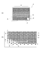
図1は、第1の実施形態に係るパワーMOS−FET1を示す模式図である。ただし、同図中には、ソース電極のない表面が模式的に示されている。また、以下の説明において、図7(a)および図8(a)についても同様である。
(First embodiment)
FIG. 1 is a schematic diagram showing a power MOS-
図1(a)は、パワーMOS−FET1の主面(チップ面)を模式的に示す平面図である。チップ面の中央には、MOS−FETのユニットセルが複数配置されたセル領域8が設けられている。また、同図中の右下隅には、ゲートパッド9が配置されている。
FIG. 1A is a plan view schematically showing the main surface (chip surface) of the power MOS-
図1(b)は、図1(a)中に破線で示すA領域のセル配置を拡大して示す模式図である。セル領域8に配置されたユニットセル3は、トレンチゲート2によって個々に画されている。また、各ユニットセル3の中央には、第1コンタクトホール4が設けられている。
FIG.1 (b) is a schematic diagram which expands and shows the cell arrangement | positioning of A area shown with a broken line in Fig.1 (a). The
一方、セル領域8を囲む終端領域7(トレンチゲート2が設けられていない領域)には、第2コンタクトホール5が、例えば、セル領域と同じ間隔で設けられている。さらに、セル領域8が外側へ突出するセル領域8のコーナー部Eに隣接した終端領域7の幅は広く設けられている。これにより、図1(b)中に示すように、セル領域8のコーナー部Eに隣接した終端領域7における第2コンタクトホール5の数は、セル領域8のコーナー部E以外の部分に隣接した終端領域7に設けられた第2コンタクトホール5の数よりも多くなっている。
On the other hand, in the termination region 7 (the region where the
ここで、第1コンタクトホール4と第2コンタクトホール5とを区別するのは、それぞれが設けられた場所が、異なるからである。すなわち、第1コンタクトホール4はセル領域に設けられ、第2コンタクトホール5は終端領域に設けられている。また、以下の説明においても、「第1コンタクト領域」は、セル領域に設けられ、「第2コンタクト領域」は終端領域7に設けられたものとする。
Here, the reason why the
MOS−FETのアバランシェ耐量を高くする場合、ターンオフ時のブレイクダウンが素子の特定箇所に集中しないように設計することが望ましい。なぜなら、ブレイクダウン局所的に発生すると、その場所にアバランシェ電流が集中し素子が破壊に至る可能性が高いからである。したがって、電界が集中してブレイクダウンが起こり易い場所を、チップ面内の複数の場所に分散させるロバストな構造設計を採ることが望ましい。 In order to increase the avalanche resistance of the MOS-FET, it is desirable to design so that breakdown at turn-off does not concentrate on a specific portion of the element. This is because if breakdown occurs locally, the avalanche current is concentrated at that location, and the device is likely to be destroyed. Therefore, it is desirable to adopt a robust structural design in which places where breakdown is likely to occur due to concentration of electric field are distributed to a plurality of places within the chip surface.
例えば、電界分布の対称性が崩れ、電界集中が生じ易い終端領域7の耐圧を高くすることが望ましい。中でも、セル領域8が外側へ突出するコーナー部Eにおいて、電界集中が生じる傾向が強く、高耐量化を図ることが望まれる。また、図1(a)中に示すF領域およびG領域においても、図1(b)に示すA領域と同じように高耐圧化を図ることが望まれる。
For example, it is desirable to increase the breakdown voltage of the
本実施形態に係るMOS−FET1では、図1(b)に示すように、セル領域8に設けられた第1コンタクトホール4と同じサイズの第2コンタクトホール5を終端領域7に設けることにより、終端部のアバランシェ耐量を向上させることができる。さらに、セル領域8のコーナー部Eに隣接した部分おいて、他の部分よりも終端領域7の幅を広くすることにより、数多く第2コンタクトホール5を設けることができる。これにより、コーナー部Eに隣接した部分のコンタクト抵抗を低下させて、アバランシェ耐量を向上させることができる。
In the MOS-
後述するように、終端領域7のコンタクト構造をホールコンタクトとすることにより、イオン注入の深さをセル領域8と同じか、または浅くすることが可能となり、終端領域7のアバランシェ耐量の低下を防ぐことができる。また、コーナー部Eに隣接した部分において、第2コンタクトホールを数多く設けることにより、コンタクト抵抗を低くすることができる。これにより、MOS−FET内部の高電界領域で発生する正孔の排出をスムーズにして、さらにアバランシェ耐量を向上させることができる。
As will be described later, by making the contact structure of the termination region 7 a hole contact, the depth of ion implantation can be made the same as or shallower than that of the
例えば、終端領域7の第2コンタクトホール5間のピッチを、フォトリソグラフィでレジストパターンの形状が維持できる限界まで狭く設けることができる。これにより、終端領域7のコンタクト抵抗を最小とすることが可能であり、アバランシェ耐量をより向上させることができる。これは、光学的シミュレーション、およびプロセスシミュレーション、デバイスシミュレーションを用いてマスク寸法を最適化することにより実施することができる。
For example, the pitch between the second contact holes 5 in the
図2は、第1実施形態に係るMOS−FET1の断面を示す模式図である。同図中に示す断面は、図1(b)中に示したB−B線に沿った断面である。以下の説明において、N型は第1導電型に対応し、P型は第2導電型に対応する。また、後述する実施形態においても同様である。
FIG. 2 is a schematic diagram showing a cross section of the MOS-
本実施形態に係るMOS−FETは、N型の第1半導体層であるドレイン層11と、ドレイン層11の第1の主面上に設けられたN型の第2半導体層であるドリフト層12と、を備えている。ドリフト層12の上部には、P型の第3の半導体層であるベース層13が設けられている。また、P型ベース層13の表面には、N型ソース領域14が設けられている。
The MOS-FET according to this embodiment includes a
さらに、N型ドレイン層11の第2の主面との間で電気的に接続された第1の主電極であるドレイン電極15と、N型ソース領域14に電気的に接続された第2の主電極であるソース電極16が設けられている。
Furthermore, a
図2中に示すように、N型ソース領域14は、ドレイン電極15とソース電極16との間で、縦方向に主電流が流れるセル領域8に設けられている。セル領域8には、N型ソース領域14の表面からN型ドリフト層12に達するトレンチゲート2と、トレンチゲート2により画された複数のユニットセル3と、が設けられている(図1(b)参照)。
As shown in FIG. 2, the N-
さらに、複数のユニットセル3のそれぞれの中央部のベース層13には、第1コンタクトホール4が設けられている。また、第1コンタクトホール4の底部には、P型の不純物がイオン注入された第1コンタクト領域21が設けられている。第1コンタクト領域21は、ソース電極16とP型ベース層13とを電気的に接続する。
Further, the
一方、セル領域の周辺に設けられた終端領域のベース層13には、複数の第2コンタクトホール5が形成されている。第2コンタクトホールの底部には、セル領域8に設けられた第1コンタクトホール4と同様に、P型の不純物がイオン注入された第2コンタクト領域22が設けられている。第2コンタクト領域22も、ソース電極16とP型ベース層13とを電気的に接続している。
On the other hand, a plurality of second contact holes 5 are formed in the
本実施形態に係るMOS−FET1では、第2コンタクトホール5は、第1コンタクトホール4と開口面積が等しくなるように設けられている。これにより、N型ドリフト層12と第1コンタクト領域21との間隔X1と、N型ドリフト層12と第2コンタクト領域22との間隔X2と、が等しくなる。つまり、P型ベース層13とN型ドリフト層12との界面であるPN接合と、第1コンタクト領域21と、の間の間隔X1が、第2コンタクト領域22とPN接合との間隔X2と等しくなる。
In the MOS-
本発明者の知見によれば、P型の不純物をイオン注入して形成される第1コンタクト領域21および第2コンタクト領域22のN型ドレイン層11方向の深さは、それぞれのコンタクトホールの開口面積に依存して変化する。例えば、第1コンタクトホール4の開口面積を、第2コンタクトホール5の開口面積よりも大きくすれば、第1コンタクト領域21とPN接合との間の間隔X1は、第2コンタクト領域22とPN接合との間隔X2よりも狭くなる。
According to the knowledge of the present inventor, the depth of the
一方、第1コンタクト領域21または第2コンタクト領域22からN型ドレイン層11に向かう方向の電界分布の最大値は、PN接合とコンタクト領域との間の間隔X1およびX2が狭いほど高くなる。したがって、PN接合とコンタクト領域との間隔が狭くなるとアバランシェ降伏が生じやすくなりアバランシェ耐量が低下する傾向にある。
On the other hand, the maximum value of the electric field distribution in the direction from the
図9は、比較例に係るMOS−FET30の断面を示す模式図である。本比較例のMOS−FET30では、同図中に示すように、終端領域7の広い面積をエッチングしてコンタクト領域52を形成している。したがって、コンタクト領域52のP型不純物は深くイオン注入され、PN接合との間隔X5は、セル領域に設けられた第1コンタクト領域21とPN接合との間隔X1より狭くなる傾向がある。
FIG. 9 is a schematic diagram showing a cross section of a MOS-
これにより、終端領域7のアバランシェ耐量が、セル領域8のアバランシェ耐量よりも低くなる傾向にあった。特に、電界集中が生じやすいコーナー部Eにおいて、アバランシェ耐量の低下が生じ易い傾向にあった。
As a result, the avalanche resistance of the
これに対して、本実施形態に係るMOS−FET1では、終端領域に第2コンタクトホール5を設けて、第2コンタクト領域22とPN接合との間隔X2が、第1コンタクト領域21とPN接合との間隔X1より狭くならないようにしている。
In contrast, in the MOS-FET1 according to the present embodiment, the
また、本実施形態に係るMOS−FET1では、X1とX2とが等しくなるように、第1コンタクトホール4と第2コンタクトホール5との開口面積を同じに設けているが、第1コンタクトホール4の開口面積を第2コンタクトホール5の開口面積よりも大きくして、X1がX2より狭くなるようにしてもよい。これにより、終端領域7のアバランシェ耐量をセル領域8よりも高くすることが可能となる。
Further, the MOS-FET1 according to the present embodiment, so that the X 1 and X 2 equal, are provided with the
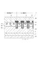
図3〜図6は、第1実施形態に係るMOS−FET1の製造工程を模式的に示す断面図である。各図中に示す断面は、図1(b)中に示したB−B線に沿った断面である。本具体例のMOS−FET1は、シリコンを材料とするシリコンMOS−FETである。
3 to 6 are cross-sectional views schematically showing manufacturing steps of the MOS-
図3(a)に示すように、N型ドレイン層11の第1の主面上にエピタキシャル成長したN型ドリフト層12に、トレンチ26を形成し、ゲート電極となる導電性のポリシリコン28を埋め込む。ポリシリコン28は、トレンチ26を形成したN型ドリフト層の全面にCVD法を用いて形成する。その後、トレンチ26内に残される部分を除いて、エッチングにより除去する。
As shown in FIG. 3A, a
N型ドレイン層11としては、シリコン基板上にエピタキシャル成長した高濃度のシリコン層、または高濃度にドープされたシリコン基板を用いることができる。また、トレンチ26の内面には、ゲート絶縁膜18となるシリコン酸化膜SiO2を形成する。
As the N-
次に、図3(b)に示すように、N型ドリフト層12の表面にP型不純物をイオン注入してP型ベース層13を形成する。P型不純物として、例えば、ボロン(B)を用いることができる。また、イオン注入後にシリコン基板を熱処理することにより、P型不純物を、N型ドリフト層12の表面から所定の深さまで拡散させる。これにより、同図中に示すP型ベース層13が形成される。
Next, as shown in FIG. 3B, a P-
続いて、図4(a)に示すように、N型不純物、例えば、ヒ素(As)を、P型ベース層13の表面にイオン注入し、N型ソース領域を形成する。この際、選択注入を行うための注入マスク31として、フォトレジストを用いることができる。
Subsequently, as shown in FIG. 4A, an N-type impurity such as arsenic (As) is ion-implanted into the surface of the P-
さらに、図4(b)に示すように、P型ベース層13およびN型ソース領域14、ポリシリコン28の表面に、層間絶縁膜17を形成する。なお、N型ソース領域14に注入されたN型不純物は、層間絶縁膜17を形成する過程で実施される熱処理により活性化することができる。また、層間絶縁膜17には、第1コンタクトホール4および第2コンタクトホール5を形成するための開口32を形成する。
Further, as shown in FIG. 4B, an
次に、図5(a)に示すように、開口32が形成された層間絶縁膜17をマスクとして、N型ソース領域14およびP型ベース層13の表面をドライエッチングして、第1コンタクトホール4および第2コンタクトホール5を形成する。ドライエッチングの方法としては、例えばリアクティブ・イオン・エッチング(RIE)法を用いることができる。また、ドライエッチングは、セル領域8に形成される第1コンタクトホール4が、N型ソース領域14を貫通してP型ベース層13に連通するまで実施する。
Next, as shown in FIG. 5A, the surface of the N-
次に、層間絶縁膜17を注入マスクとして、P型不純物、例えば、ボロン(B)をイオン注入する。P型不純物は、第1コンタクトホールの底部と、第2コンタクトホールの底部と、の両方に同時にイオン注入され、第1コンタクト領域21および第2コンタクト領域22が形成される。
Next, using the
この際、セル領域8と終端領域7とにおいて、層間絶縁膜17に設けられた開口32の開口面積を変えることにより、イオン注入により形成される第1コンタクト領域21と第2コンタクト領域22とを、異なる深さに形成することができる。すなわち、層間絶縁膜17の開口32を形成する際に用いるフォトマスクの設計を変更するだけで、製造工程を変更することなく、第1コンタクト領域21の深さと第2コンタクト領域22の深さとを変えることができる。これにより、前述したように、終端領域7におけるアバランシェ耐量を、セル領域8と同じか、または高くすることが可能となる。
At this time, the
次に、図6(a)に示すように、層間絶縁膜17の表面を所定量エッチングし、N型ソース領域14の表面の一部を露出させる。また、終端領域7に形成された層間絶縁膜17をエッチングして除去する。
Next, as shown in FIG. 6A, a predetermined amount of the surface of the
さらに、図6(b)に示すように、セル領域8のN型ソース領域14、第1コンタクトホール4、層間絶縁膜17、および、終端領域のP型ベース層13、第2コンタクトホール5を覆って、ソース電極16を形成する。これにより、セル領域8において、ソース電極16とP型ベース層13とが第1コンタクト領域21を介して電気的に接続され、P型ベース層13の電位が固定されるので、MOS−FET1の動作を安定させることができる。また、終端領域7において、第2コンタクト領域22を介してソース電極16とP型ベース層13との間が低抵抗に接続されるので、ホールの排出抵抗が小さくなり、アバランシェ耐量を向上させることができる。
Further, as shown in FIG. 6B, the N-
一方、図6(b)中に示すように、N型ドレイン層11の第2の主面には、ドレイン電極15が形成される。具体的には、MOS−FET1が形成されたシリコン基板の裏面を研削して薄板化し、メタライズすることにより、ドレイン電極15を形成する。
On the other hand, as shown in FIG. 6B, the
(第2の実施形態)
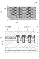
図7は、第2の実施形態に係るMOS−FET10を示す模式図である。図7(a)は、MOS−FETチップのコーナー部Eの周辺を模式的に示す平面図である。また、図7(b)は、図7(a)中に示したC−C線に沿った断面を示す模式図である。
(Second Embodiment)
FIG. 7 is a schematic diagram showing a MOS-
図7(a)および(b)に示すように、セル領域8では、トレンチゲート2で画されたユニットセル3が設けられ、ユニットセル3の中央に第1コンタクトホール4が設けられている点で、第1の実施形態に示したMOS−FET1と同じである。
As shown in FIGS. 7A and 7B, in the
一方、セル領域8の周辺の終端部には、第1コンタクトホール4よりも開口面積が小さい第2コンタクトホール35が設けられている。また、第2コンタクトホール35は、MOS−FET1に比べて狭いピッチで、数多く設けられている。これにより、終端部7において、ソース電極16とP型ベース層13との間のコンタクト抵抗が低く維持されている。
On the other hand, a
また、セル領域8が外側に突出するコーナー部Eに隣接した部分においては、セル領域8のそれ以外の部分に隣接した部分よりも終端領域7の幅が広い。そして、第2コンタクトホール35は、コーナー部Eに隣接した部分と、それ以外の部分と、において同一のピッチで形成されている。つまり、本実施形態に係るMOS−FET10においても、第2コンタクトホール35の数は、セル領域8のコーナー部E以外の部分に隣接した終端領域7に設けられた第2コンタクトホール35の数よりも、セル領域8のコーナー部Eに隣接した終端領域7においてさらに多く設けられている。したがって、ソース電極16とP型ベース層13との間の抵抗がさらに低くなり、正孔の排出抵抗がより小さくなる。これにより、コーナー部Eでの電界集中によるアバランシェ耐量の低下を防ぐことができる。
Further, in the portion adjacent to the corner portion E where the
また、図7(b)に示すように、第2コンタクトホール35の開口面積が、第1コンタクトホール4の開口面積よりも小さいことから、第1コンタクト領域21の深さよりも、第2コンタクト領域38の深さの方が浅くなっている。すなわち、第1コンタクト領域21とPN接合との間隔X1よりも、第2コンタクト領域38とPN接合との間隔X3の方が広くなっており、終端領域7のアバランシェ耐量が高くなっている。
Further, as shown in FIG. 7B, since the opening area of the
本実施形態に係るMOS−FET10では、開口面積の小さい第2コンタクトホール35を多数設けることにより、ソース電極16とP型ベース層13との間のコンタクト抵抗を小さくし、さらに、第2コンタクト領域38を浅く形成してアバランシェ耐量を高めることによって、終端領域7で発生するアバランシェ降伏を抑えることができる。
In the MOS-
また、前述したように、第2コンタクトホール35のピッチを狭く形成することにより、図7(b)中に示すように、隣接する第2コンタクト領域38が一体となり、1つのコンタクト領域となるように形成することもできる。これにより、さらにソース電極とP型ベース層のコンタクト抵抗を下げることが可能となり、アバランシェ耐量の向上を図ることができる。第2コンタクトホール35のピッチは、フォトリソグラフィにおいて開口パターンの形状を維持できる限界まで狭く形成することが可能である。
Further, as described above, by forming the pitch of the second contact holes 35 to be narrow, as shown in FIG. 7B, the adjacent
(第3の実施形態)
図8は、第3の実施形態に係るMOS−FET20を示す模式図である。図8(a)は、MOS−FETチップのセル領域8を模式的に示す平面図である。また、図8(b)は、図8(a)中に示したD−D線に沿った断面を示す模式図である。
(Third embodiment)
FIG. 8 is a schematic diagram showing a MOS-
図8(a)に示すように、本実施形態に係るMOS−FET20では、セル領域8内に、第1コンタクトホール4よりも開口面積の大きい複数の第3コンタクトホール42が設けられた複数のユニットセル45を有している。一方、図示しない終端領域には、第1の実施形態または第2の実施形態に関して前述したように、第1コンタクトホール4と開口面積が同じか、または小さい第2コンタクトホールが設けられている。
As shown in FIG. 8A, in the MOS-
また、図8(b)の断面図に示すように、第3コンタクトホール42の底部に設けられた第3コンタクト領域43のN型ドレイン層11方向の深さは、第1コンタクトホール4の底部に設けられた第1コンタクト領域21の深さよりも深くなっている。すなわち、第3コンタクト領域43と、P型ベース層13とN型ドリフト層12との境界のPN接合と、の間隔X4は、第1コンタクト領域21とPN接合との間隔X1よりも狭くなっている。
8B, the depth of the
したがって、第3コンタクトホール42が設けられたユニットセル45のアバランシェ耐量は、第1コンタクトホール4が設けられたユニットセル3よりも低くなる。一方、終端領域のアバランシェ耐量は、第1の実施形態または第2の実施形態に関して前述したように、ユニットセル3よりも高くなっている。つまり、第3コンタクトホール42が設けられたユニットセル45において、アバランシェ耐量が最も低くなり、アバランシェ降伏が生じ易くなっている。
Therefore, the avalanche resistance of the
すなわち、本実施形態に係るMOS−FET20では、ターンオフ時に過剰な電圧が加わった場合に、セル領域8に複数配置されたユニットセル45において、積極的にアバランシェ降伏を起こさせることができる。これにより、アバランシェ電流を分散させて電流集中を防ぎ、素子破壊を回避することができる。
That is, in the MOS-
ここで、個々のユニットセル45に流れるアバランシェ電流が、素子破壊に至る限界値を超えないように、セル領域8に設けられるユニットセル45の数と配置位置とを、デバイスシミュレーション技術を用いて最適化するとよい。
Here, the number and arrangement positions of the
このように本実施形態に係るMOS−FET20では、ソース電極16とP型ベース層13との間のコンタクト構造を最適化することにより、アバランシェ電流を均一に拡散させることが可能であり、素子破壊を有効に回避することができる。また、これを実施するために製造工程が増えることはなく、歩留りの改善も可能であるから、製造コストを低減することが可能である。
As described above, in the MOS-
以上、本発明に係る一実施形態を参照して本発明を説明したが、本発明はこれらの実施形態に限定されるものではない。例えば、出願時の技術水準に基づいて、当業者がなし得る設計変更や、材料の変更等、本発明と技術的思想を同じとする実施態様も本発明の技術的範囲に含有される。 As mentioned above, although this invention was demonstrated with reference to one embodiment which concerns on this invention, this invention is not limited to these embodiment. For example, embodiments that have the same technical idea as the present invention, such as design changes and material changes that can be made by those skilled in the art based on the technical level at the time of filing, are also included in the technical scope of the present invention.
例えば、上記の実施態様に示したNチャネルのMOS−FETのみならず、PチャネルのMOS−FETにも適用できる。また、シリコンを材料とするMOS−FETに限られる訳ではなく、SiCやGaN等を材料とする半導体装置にも適用可能である。 For example, the present invention can be applied not only to the N-channel MOS-FET shown in the above embodiment but also to a P-channel MOS-FET. Further, the present invention is not limited to a MOS-FET made of silicon, but can be applied to a semiconductor device made of SiC, GaN, or the like.
1、10、20 MOS−FET
2 トレンチゲート
3、45 ユニットセル
4 第1コンタクトホール
5、35 第2コンタクトホール
7 終端領域
8 セル領域
9 ゲートパッド
11 N型ドレイン層
12 N型ドリフト層
13 P型ベース層
14 N型ソース領域
15 ドレイン電極
16 ソース電極
17 層間絶縁膜
18 ゲート絶縁膜
21 第1コンタクト領域
22、38 第2コンタクト領域
26 トレンチ
28 ポリシリコン
42 第3コンタクトホール
43 第3コンタクト領域
E コーナー部
1, 10, 20 MOS-FET
2
Claims (5)
前記第1半導体層の第1の主面上に設けられた第1導電型の第2半導体層と、
前記第2半導体層上に設けられた第2導電型の第3半導体層と、
前記第3半導体層の表面に設けられた第1導電型のソース領域と、
前記第1半導体層の第2の主面に電気的に接続された第1の主電極と、
前記ソース領域に電気的に接続された第2の主電極と、
前記第1の主電極と前記第2の主電極との間で前記ソース領域を介して縦方向に主電流が流れるセル領域に設けられた複数のユニットセルを画し、前記第3半導体層の表面から前記第2の半導体層に達して設けられたトレンチゲートと、
前記複数のユニットセルのそれぞれの中央部において前記第3の半導体層に形成された第1のコンタクトホールの底部にイオン注入された第2導電型の不純物を含み、前記第2の主電極と前記第3半導体層とを電気的に接続する第1コンタクト領域と、
前記セル領域の周囲に設けられた終端領域において前記第3の半導体層に形成された複数の第2コンタクトホールの底部にイオン注入された第2導電型の不純物を含み、前記第2の主電極と前記第3半導体層とを電気的に接続する第2コンタクト領域と、
を備え、
前記第2コンタクトホールの開口面積は、前記第1コンタクトホールの開口面積と等しいか、または前記第1コンタクトホールの開口面積よりも小さいことを特徴とする半導体装置。 A first semiconductor layer of a first conductivity type;
A second semiconductor layer of the first conductivity type provided on the first main surface of the first semiconductor layer;
A third semiconductor layer of a second conductivity type provided on the second semiconductor layer;
A source region of a first conductivity type provided on a surface of the third semiconductor layer;
A first main electrode electrically connected to a second main surface of the first semiconductor layer;
A second main electrode electrically connected to the source region;
A plurality of unit cells provided in a cell region in which a main current flows in a vertical direction through the source region between the first main electrode and the second main electrode; A trench gate provided from the surface to the second semiconductor layer;
A second conductivity type impurity ion-implanted into a bottom portion of a first contact hole formed in the third semiconductor layer at a central portion of each of the plurality of unit cells; A first contact region electrically connecting the third semiconductor layer;
The second main electrode including a second conductivity type impurity ion-implanted into the bottom of a plurality of second contact holes formed in the third semiconductor layer in a termination region provided around the cell region; And a second contact region electrically connecting the third semiconductor layer,
With
The semiconductor device according to claim 1, wherein an opening area of the second contact hole is equal to or smaller than an opening area of the first contact hole.
前記第1半導体層の第1の主面上に設けられた第1導電型の第2半導体層と、
前記第2半導体層上に設けられた第2導電型の第3半導体層と、
前記第3半導体層の表面に設けられた第1導電型のソース領域と、
前記第1半導体層の第2の主面に電気的に接続された第1の主電極と、
前記ソース領域に電気的に接続された第2の主電極と、
前記第1の主電極と前記第2の主電極との間で前記ソース領域を介して縦方向に主電流が流れるセル領域に設けられた複数のユニットセルを画し、前記第3半導体層の表面から前記第2の半導体層に達して設けられたトレンチゲートと、
を有する半導体装置の製造方法であって、
前記複数のユニットセルのそれぞれの中央部において前記第3の半導体層に形成された第1コンタクトホールの底部と、前記セル領域の周囲に設けられた終端領域において前記第3の半導体層に形成された第2コンタクトホールの底部と、に、第2導電型の不純物を同時にイオン注入することを特徴とする半導体装置の製造方法。 A first semiconductor layer of a first conductivity type;
A second semiconductor layer of the first conductivity type provided on the first main surface of the first semiconductor layer;
A third semiconductor layer of a second conductivity type provided on the second semiconductor layer;
A source region of a first conductivity type provided on a surface of the third semiconductor layer;
A first main electrode electrically connected to a second main surface of the first semiconductor layer;
A second main electrode electrically connected to the source region;
A plurality of unit cells provided in a cell region in which a main current flows in a vertical direction through the source region between the first main electrode and the second main electrode; A trench gate provided from the surface to the second semiconductor layer;
A method of manufacturing a semiconductor device having
Formed in the third semiconductor layer at the bottom of the first contact hole formed in the third semiconductor layer at the center of each of the plurality of unit cells and at the termination region provided around the cell region. A method of manufacturing a semiconductor device, wherein a second conductivity type impurity is simultaneously ion-implanted into the bottom of the second contact hole.
Priority Applications (2)
| Application Number | Priority Date | Filing Date | Title |
|---|---|---|---|
| JP2009255078A JP2011100877A (en) | 2009-11-06 | 2009-11-06 | Semiconductor device and method of manufacturing the same |
| US12/885,395 US8350322B2 (en) | 2009-11-06 | 2010-09-17 | Semiconductor device and method for manufacturing the same |
Applications Claiming Priority (1)
| Application Number | Priority Date | Filing Date | Title |
|---|---|---|---|
| JP2009255078A JP2011100877A (en) | 2009-11-06 | 2009-11-06 | Semiconductor device and method of manufacturing the same |
Publications (2)
| Publication Number | Publication Date |
|---|---|
| JP2011100877A true JP2011100877A (en) | 2011-05-19 |
| JP2011100877A5 JP2011100877A5 (en) | 2012-04-26 |
Family
ID=43973520
Family Applications (1)
| Application Number | Title | Priority Date | Filing Date |
|---|---|---|---|
| JP2009255078A Pending JP2011100877A (en) | 2009-11-06 | 2009-11-06 | Semiconductor device and method of manufacturing the same |
Country Status (2)
| Country | Link |
|---|---|
| US (1) | US8350322B2 (en) |
| JP (1) | JP2011100877A (en) |
Cited By (9)
| Publication number | Priority date | Publication date | Assignee | Title |
|---|---|---|---|---|
| JP2016111207A (en) * | 2014-12-08 | 2016-06-20 | 三菱電機株式会社 | Power semiconductor device |
| US9698221B2 (en) | 2014-05-01 | 2017-07-04 | Mitsubishi Electric Corporation | Semiconductor device |
| WO2017138505A1 (en) * | 2016-02-12 | 2017-08-17 | パナソニック株式会社 | Semiconductor device |
| JP2019161190A (en) * | 2018-03-16 | 2019-09-19 | 株式会社東芝 | Semiconductor device |
| JP2020102540A (en) * | 2018-12-21 | 2020-07-02 | トヨタ自動車株式会社 | Semiconductor device |
| JP2020170807A (en) * | 2019-04-04 | 2020-10-15 | 富士電機株式会社 | Semiconductor device and method for manufacturing semiconductor device |
| JP2021044462A (en) * | 2019-09-13 | 2021-03-18 | 株式会社 日立パワーデバイス | Semiconductor device and power conversion device |
| JPWO2020145109A1 (en) * | 2019-01-08 | 2021-09-30 | 三菱電機株式会社 | Semiconductor equipment and power conversion equipment |
| JP7332812B2 (en) | 2020-08-11 | 2023-08-23 | 三菱電機株式会社 | Silicon carbide semiconductor device and power conversion device |
Families Citing this family (9)
| Publication number | Priority date | Publication date | Assignee | Title |
|---|---|---|---|---|
| JP2011176026A (en) * | 2010-02-23 | 2011-09-08 | Fuji Electric Co Ltd | Method of manufacturing semiconductor element |
| JP2013065749A (en) * | 2011-09-20 | 2013-04-11 | Toshiba Corp | Semiconductor device |
| JP5566540B2 (en) * | 2011-09-21 | 2014-08-06 | 三菱電機株式会社 | Power semiconductor device |
| US10249721B2 (en) | 2013-04-04 | 2019-04-02 | Infineon Technologies Austria Ag | Semiconductor device including a gate trench and a source trench |
| US9214546B2 (en) * | 2013-05-29 | 2015-12-15 | Panasonic Intellectual Property Management Co., Ltd. | Silicon carbide switching device with novel overvoltage detection element for overvoltage control |
| US9666663B2 (en) * | 2013-08-09 | 2017-05-30 | Infineon Technologies Ag | Semiconductor device with cell trench structures and contacts and method of manufacturing a semiconductor device |
| JP6168961B2 (en) * | 2013-10-10 | 2017-07-26 | 三菱電機株式会社 | Semiconductor device |
| US9178015B2 (en) * | 2014-01-10 | 2015-11-03 | Vishay General Semiconductor Llc | Trench MOS device having a termination structure with multiple field-relaxation trenches for high voltage applications |
| CN113690337B (en) * | 2021-09-13 | 2023-12-08 | 武汉新芯集成电路制造有限公司 | Single photon avalanche diode, manufacturing method thereof and single photon avalanche diode array |
Citations (6)
| Publication number | Priority date | Publication date | Assignee | Title |
|---|---|---|---|---|
| JPH04229661A (en) * | 1990-06-08 | 1992-08-19 | Nippondenso Co Ltd | Insulated-gate bipolar transistor and its manufacture |
| JPH05102487A (en) * | 1991-10-07 | 1993-04-23 | Nippondenso Co Ltd | Vertical semiconductor device |
| JP2000101085A (en) * | 1998-09-18 | 2000-04-07 | Siemens Ag | Edge structure with high breakdown strength for semiconductor module |
| JP2005019734A (en) * | 2003-06-26 | 2005-01-20 | Renesas Technology Corp | Semiconductor device and its manufacturing method |
| JP2006526286A (en) * | 2003-05-31 | 2006-11-16 | コーニンクレッカ フィリップス エレクトロニクス エヌ ヴィ | Semiconductor device having termination structure and method of manufacturing the same |
| JP2008117826A (en) * | 2006-11-01 | 2008-05-22 | Toshiba Corp | Power semiconductor element |
Family Cites Families (2)
| Publication number | Priority date | Publication date | Assignee | Title |
|---|---|---|---|---|
| JP2003086801A (en) | 2001-09-13 | 2003-03-20 | Sanyo Electric Co Ltd | Insulation gate type semiconductor device and method of manufacturing the same |
| JP2004281524A (en) | 2003-03-13 | 2004-10-07 | Sanyo Electric Co Ltd | Semiconductor device |
-
2009
- 2009-11-06 JP JP2009255078A patent/JP2011100877A/en active Pending
-
2010
- 2010-09-17 US US12/885,395 patent/US8350322B2/en active Active
Patent Citations (6)
| Publication number | Priority date | Publication date | Assignee | Title |
|---|---|---|---|---|
| JPH04229661A (en) * | 1990-06-08 | 1992-08-19 | Nippondenso Co Ltd | Insulated-gate bipolar transistor and its manufacture |
| JPH05102487A (en) * | 1991-10-07 | 1993-04-23 | Nippondenso Co Ltd | Vertical semiconductor device |
| JP2000101085A (en) * | 1998-09-18 | 2000-04-07 | Siemens Ag | Edge structure with high breakdown strength for semiconductor module |
| JP2006526286A (en) * | 2003-05-31 | 2006-11-16 | コーニンクレッカ フィリップス エレクトロニクス エヌ ヴィ | Semiconductor device having termination structure and method of manufacturing the same |
| JP2005019734A (en) * | 2003-06-26 | 2005-01-20 | Renesas Technology Corp | Semiconductor device and its manufacturing method |
| JP2008117826A (en) * | 2006-11-01 | 2008-05-22 | Toshiba Corp | Power semiconductor element |
Cited By (17)
| Publication number | Priority date | Publication date | Assignee | Title |
|---|---|---|---|---|
| US9698221B2 (en) | 2014-05-01 | 2017-07-04 | Mitsubishi Electric Corporation | Semiconductor device |
| JP2016111207A (en) * | 2014-12-08 | 2016-06-20 | 三菱電機株式会社 | Power semiconductor device |
| WO2017138505A1 (en) * | 2016-02-12 | 2017-08-17 | パナソニック株式会社 | Semiconductor device |
| JPWO2017138505A1 (en) * | 2016-02-12 | 2018-12-06 | パナソニック株式会社 | Semiconductor device |
| US10529843B2 (en) | 2016-02-12 | 2020-01-07 | Panasonic Corporation | Semiconductor device |
| JP2019161190A (en) * | 2018-03-16 | 2019-09-19 | 株式会社東芝 | Semiconductor device |
| JP2020102540A (en) * | 2018-12-21 | 2020-07-02 | トヨタ自動車株式会社 | Semiconductor device |
| JP6991370B2 (en) | 2019-01-08 | 2022-01-12 | 三菱電機株式会社 | Semiconductor equipment and power conversion equipment |
| JPWO2020145109A1 (en) * | 2019-01-08 | 2021-09-30 | 三菱電機株式会社 | Semiconductor equipment and power conversion equipment |
| DE112019006587T5 (en) | 2019-01-08 | 2021-12-23 | Mitsubishi Electric Corporation | SEMICONDUCTOR UNIT AND POWER CONVERTER UNIT |
| JP2020170807A (en) * | 2019-04-04 | 2020-10-15 | 富士電機株式会社 | Semiconductor device and method for manufacturing semiconductor device |
| US11387318B2 (en) | 2019-04-04 | 2022-07-12 | Fuji Electric Co., Ltd. | Semiconductor device and method of manufacturing a semiconductor device |
| JP7272071B2 (en) | 2019-04-04 | 2023-05-12 | 富士電機株式会社 | Semiconductor device and method for manufacturing semiconductor device |
| JP2021044462A (en) * | 2019-09-13 | 2021-03-18 | 株式会社 日立パワーデバイス | Semiconductor device and power conversion device |
| WO2021049090A1 (en) * | 2019-09-13 | 2021-03-18 | 株式会社日立パワーデバイス | Semiconductor device and power conversion device |
| JP7171527B2 (en) | 2019-09-13 | 2022-11-15 | 株式会社 日立パワーデバイス | Semiconductor equipment and power conversion equipment |
| JP7332812B2 (en) | 2020-08-11 | 2023-08-23 | 三菱電機株式会社 | Silicon carbide semiconductor device and power conversion device |
Also Published As
| Publication number | Publication date |
|---|---|
| US8350322B2 (en) | 2013-01-08 |
| US20110108911A1 (en) | 2011-05-12 |
Similar Documents
| Publication | Publication Date | Title |
|---|---|---|
| JP2011100877A (en) | Semiconductor device and method of manufacturing the same | |
| US9263572B2 (en) | Semiconductor device with bottom gate wirings | |
| JP4609656B2 (en) | Trench structure semiconductor device | |
| JP4892172B2 (en) | Semiconductor device and manufacturing method thereof | |
| US20110309464A1 (en) | Semiconductor device including cell region and peripheral region having high breakdown voltage structure | |
| JP5136578B2 (en) | Semiconductor device | |
| JP2013258327A (en) | Semiconductor device and method of manufacturing the same | |
| JP2009043966A (en) | Semiconductor apparatus and method of manufacturing the same | |
| JP2010067737A (en) | Semiconductor device and method of manufacturing the same | |
| JP5795452B1 (en) | Silicon carbide semiconductor device, method for manufacturing silicon carbide semiconductor device, and method for designing silicon carbide semiconductor device | |
| JP2005285913A (en) | Semiconductor device and manufacturing method thereof | |
| KR20100064556A (en) | A semiconductor device and method of manufacturing the same | |
| JPWO2014013618A1 (en) | Semiconductor device and manufacturing method thereof | |
| US9190504B2 (en) | Semiconductor device | |
| KR101667499B1 (en) | Semiconductor device and method of manufacturing the same | |
| JP4929594B2 (en) | Semiconductor device and manufacturing method of semiconductor device | |
| JP2015056643A (en) | Semiconductor device manufacturing method | |
| US20160079350A1 (en) | Semiconductor device and manufacturing method thereof | |
| JP2008153620A (en) | Semiconductor device | |
| JP2006041123A (en) | Semiconductor device | |
| JP2009277755A (en) | Semiconductor device | |
| JP2009038214A (en) | Semiconductor device | |
| JP2012059931A (en) | Semiconductor device | |
| CN114388612A (en) | Semiconductor device and method for manufacturing semiconductor device | |
| US20150364585A1 (en) | Power semiconductor device |
Legal Events
| Date | Code | Title | Description |
|---|---|---|---|
| A521 | Request for written amendment filed |
Free format text: JAPANESE INTERMEDIATE CODE: A523 Effective date: 20120308 |
|
| A621 | Written request for application examination |
Free format text: JAPANESE INTERMEDIATE CODE: A621 Effective date: 20120308 |
|
| A131 | Notification of reasons for refusal |
Free format text: JAPANESE INTERMEDIATE CODE: A131 Effective date: 20130924 |
|
| A977 | Report on retrieval |
Free format text: JAPANESE INTERMEDIATE CODE: A971007 Effective date: 20130926 |
|
| A02 | Decision of refusal |
Free format text: JAPANESE INTERMEDIATE CODE: A02 Effective date: 20140204 |