WO2015162891A1 - 有機el表示パネルの製造方法および有機el表示パネルの製造システム - Google Patents
有機el表示パネルの製造方法および有機el表示パネルの製造システム Download PDFInfo
- Publication number
- WO2015162891A1 WO2015162891A1 PCT/JP2015/002124 JP2015002124W WO2015162891A1 WO 2015162891 A1 WO2015162891 A1 WO 2015162891A1 JP 2015002124 W JP2015002124 W JP 2015002124W WO 2015162891 A1 WO2015162891 A1 WO 2015162891A1
- Authority
- WO
- WIPO (PCT)
- Prior art keywords
- foreign matter
- organic
- raw material
- material liquid
- display panel
- Prior art date
- Legal status (The legal status is an assumption and is not a legal conclusion. Google has not performed a legal analysis and makes no representation as to the accuracy of the status listed.)
- Ceased
Links
Images




Classifications
-
- H—ELECTRICITY
- H10—SEMICONDUCTOR DEVICES; ELECTRIC SOLID-STATE DEVICES NOT OTHERWISE PROVIDED FOR
- H10K—ORGANIC ELECTRIC SOLID-STATE DEVICES
- H10K71/00—Manufacture or treatment specially adapted for the organic devices covered by this subclass
- H10K71/10—Deposition of organic active material
- H10K71/12—Deposition of organic active material using liquid deposition, e.g. spin coating
- H10K71/13—Deposition of organic active material using liquid deposition, e.g. spin coating using printing techniques, e.g. ink-jet printing or screen printing
- H10K71/135—Deposition of organic active material using liquid deposition, e.g. spin coating using printing techniques, e.g. ink-jet printing or screen printing using ink-jet printing
-
- H—ELECTRICITY
- H05—ELECTRIC TECHNIQUES NOT OTHERWISE PROVIDED FOR
- H05B—ELECTRIC HEATING; ELECTRIC LIGHT SOURCES NOT OTHERWISE PROVIDED FOR; CIRCUIT ARRANGEMENTS FOR ELECTRIC LIGHT SOURCES, IN GENERAL
- H05B33/00—Electroluminescent light sources
- H05B33/10—Apparatus or processes specially adapted to the manufacture of electroluminescent light sources
-
- H—ELECTRICITY
- H10—SEMICONDUCTOR DEVICES; ELECTRIC SOLID-STATE DEVICES NOT OTHERWISE PROVIDED FOR
- H10K—ORGANIC ELECTRIC SOLID-STATE DEVICES
- H10K50/00—Organic light-emitting devices
- H10K50/10—OLEDs or polymer light-emitting diodes [PLED]
- H10K50/11—OLEDs or polymer light-emitting diodes [PLED] characterised by the electroluminescent [EL] layers
-
- H—ELECTRICITY
- H10—SEMICONDUCTOR DEVICES; ELECTRIC SOLID-STATE DEVICES NOT OTHERWISE PROVIDED FOR
- H10K—ORGANIC ELECTRIC SOLID-STATE DEVICES
- H10K59/00—Integrated devices, or assemblies of multiple devices, comprising at least one organic light-emitting element covered by group H10K50/00
- H10K59/10—OLED displays
- H10K59/12—Active-matrix OLED [AMOLED] displays
- H10K59/122—Pixel-defining structures or layers, e.g. banks
-
- H—ELECTRICITY
- H10—SEMICONDUCTOR DEVICES; ELECTRIC SOLID-STATE DEVICES NOT OTHERWISE PROVIDED FOR
- H10K—ORGANIC ELECTRIC SOLID-STATE DEVICES
- H10K71/00—Manufacture or treatment specially adapted for the organic devices covered by this subclass
-
- H—ELECTRICITY
- H10—SEMICONDUCTOR DEVICES; ELECTRIC SOLID-STATE DEVICES NOT OTHERWISE PROVIDED FOR
- H10K—ORGANIC ELECTRIC SOLID-STATE DEVICES
- H10K71/00—Manufacture or treatment specially adapted for the organic devices covered by this subclass
- H10K71/70—Testing, e.g. accelerated lifetime tests
-
- H—ELECTRICITY
- H10—SEMICONDUCTOR DEVICES; ELECTRIC SOLID-STATE DEVICES NOT OTHERWISE PROVIDED FOR
- H10K—ORGANIC ELECTRIC SOLID-STATE DEVICES
- H10K59/00—Integrated devices, or assemblies of multiple devices, comprising at least one organic light-emitting element covered by group H10K50/00
- H10K59/10—OLED displays
- H10K59/12—Active-matrix OLED [AMOLED] displays
- H10K59/1201—Manufacture or treatment
-
- H—ELECTRICITY
- H10—SEMICONDUCTOR DEVICES; ELECTRIC SOLID-STATE DEVICES NOT OTHERWISE PROVIDED FOR
- H10K—ORGANIC ELECTRIC SOLID-STATE DEVICES
- H10K71/00—Manufacture or treatment specially adapted for the organic devices covered by this subclass
- H10K71/311—Purifying organic semiconductor materials
-
- H—ELECTRICITY
- H10—SEMICONDUCTOR DEVICES; ELECTRIC SOLID-STATE DEVICES NOT OTHERWISE PROVIDED FOR
- H10K—ORGANIC ELECTRIC SOLID-STATE DEVICES
- H10K71/00—Manufacture or treatment specially adapted for the organic devices covered by this subclass
- H10K71/40—Thermal treatment, e.g. annealing in the presence of a solvent vapour
Definitions
- the present disclosure relates to a method of manufacturing an organic EL display panel and a manufacturing system of an organic EL display panel, and more particularly to a manufacturing method of an organic EL display panel in which a printing technique is adopted and a manufacturing system of the organic EL display panel.
- Patent Document 1 describes a technique of applying a raw material liquid (functional liquid) between banks (partition walls) provided on a substrate when manufacturing an organic EL display panel.
- the present disclosure relates to a method for manufacturing an organic EL display panel, and a method for manufacturing an organic EL display panel that can deal with foreign matter adhered to a substrate before a printing process, An organic EL display panel manufacturing system is provided.
- a method for manufacturing an organic EL display panel includes a printing process in which a raw material liquid containing an organic EL material is applied between the banks of a substrate provided with a plurality of banks.
- a method of manufacturing an EL display panel comprising: a detection step of detecting foreign matter present on the bank side surface of the substrate before the printing step; and a step of detecting the foreign matter on the substrate when the foreign matter is detected.
- An information generating step for generating position information indicating a position, and a resin based on the position information, and applying an inhibitory resin that inhibits the foreign substance from absorbing the raw material liquid to at least one of the foreign substance and the periphery thereof Application step.
- the absorption of the raw material liquid by the foreign matter is suppressed, and in the organic EL display panel that is the product, the portion with no foreign matter attached The difference in luminance can be reduced.
- FIG. 1 is a perspective view schematically showing a substrate during manufacture of an organic EL display panel.
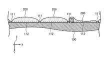
- FIG. 2 is a cross-sectional view schematically showing a substrate to which foreign matter has adhered immediately after the printing process is performed.
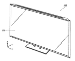
- FIG. 3 is a perspective view showing a television provided with an organic EL display panel.
- FIG. 4 is a diagram schematically showing a manufacturing system of an organic EL display panel.
- FIG. 5 is a flowchart showing a method for manufacturing an organic EL display panel.
- FIG. 6 is a side view schematically showing a resin coating apparatus that performs the resin coating process.
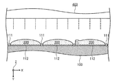
- FIG. 7 is a side view schematically showing a printing apparatus that executes the printing process.
- FIG. 1 is a perspective view schematically showing a substrate during manufacture of an organic EL display panel.
- FIG. 2 is a cross-sectional view schematically showing a substrate to which foreign matter has adhered immediately after the printing process is performed.
- FIG. 3 is a perspective view showing a television provided
- FIG. 8 is a perspective view schematically showing the substrate after the resin application step in Modification 1 of Embodiment 1.
- FIG. 9 is a side view schematically illustrating a printing apparatus that executes a printing process according to the second modification of the first embodiment.
- FIG. 10 is a diagram schematically illustrating an organic EL display panel manufacturing system according to the second embodiment.
- FIG. 11 is a flowchart illustrating a method of manufacturing the organic EL display panel according to the second embodiment.
- FIG. 12 is a side view schematically illustrating a printing apparatus that performs the printing process according to the second embodiment.
- FIG. 1 is a perspective view schematically showing a substrate during manufacture of an organic EL display panel.
- a substrate 100 shown in the figure is the substrate 100 immediately before entering the printing process, and a vertical bank 111 which is a bank 101 (partition wall) arranged extending in the vertical direction (Z-axis direction in the drawing) on the surface of the substrate 100. And a horizontal bank 112, which is a bank 101 arranged extending in the horizontal direction (X-axis direction in the drawing), are provided in a grid pattern.
- a vertical bank 111 which is a bank 101 (partition wall) arranged extending in the vertical direction (Z-axis direction in the drawing) on the surface of the substrate 100.
- a horizontal bank 112 which is a bank 101 arranged extending in the horizontal direction (X-axis direction in the drawing) are provided in a grid pattern.
- FIG. 1 the foreign matter A attached to the substrate 100 at any stage before the printing process is shown for explanation, but the foreign matter A is accidentally attached to the substrate 100 with a certain probability.
- the volume of the light emitting pixel 102 where the foreign matter A exists is Since the volume of the light emitting pixel 102 in which A does not exist is reduced by the amount of the foreign matter A, generally, the amount of the raw material liquid 200 applied to the light emitting pixel 102 in which the foreign matter A exists is set to light emission in which the foreign matter A does not exist A measure of reducing the amount of the raw material liquid 200 applied to the pixel 102 can be considered.
- the inventor conducted diligent experiments and research under various conditions for reducing the amount of the raw material liquid to be applied to the light emitting pixel 102 where the foreign matter A exists, and optimized the application condition of the raw material liquid. It has been found that when the amount of the raw material liquid applied to the light emitting pixel 102 in which the presence of light is reduced, the luminance of the light emitting pixel 102 in which the foreign matter A exists tends to be higher than the luminance of the light emitting pixel 102 that does not exist.
- the luminance of the light emitting pixel 102 in which the foreign matter A exists is increased because the thickness of the layer formed by the application of the raw material liquid 200 is decreased.
- the raw material liquid 200 is held in a state of being attracted to the foreign matter A by a phenomenon called foreign matter A capillary phenomenon as shown in FIG. It has been found that the amount of the raw material liquid 200 is reduced. That is, a new finding is obtained that the presence of the foreign matter A in the light emitting pixel 102 does not decrease the volume of the light emitting pixel 102 but conversely increases the volume of the light emitting pixel 102. It was.
- the organic EL display panel 300 is a device that displays video, images, characters, and the like as shown in FIG. 3, for example, and is a display device manufactured from the substrate 100 as shown in FIG. For example, the organic EL display panel 300 is incorporated in a television 399 that outputs an image obtained from a received broadcast wave or the like.
- the organic EL display panel 300 includes, as a light emitting element, an organic EL (Electro Luminescence) diode that is a light emitting diode having a light emitting layer made of an organic EL material.
- a method for forming a light emitting layer with an organic EL material is a printing method.
- a plurality of types (three types in this embodiment) including organic EL materials corresponding to each emission color are included.
- a printing method in which the raw material liquid 200 is discharged between the predetermined banks 101 to fill the raw material liquid 200 is employed.
- FIG. 4 is a diagram schematically showing a manufacturing system of an organic EL display panel.
- the manufacturing system 400 includes a detection device 401, a resin coating device 402, and a printing device 403.
- each of the devices are connected by a transfer device, and each of the devices may be arranged in a chamber.
- the detection device 401 is a device that detects the foreign matter A existing on the surface of the substrate 101 on the side of the bank 101 on which the plurality of banks 101 are provided in the previous process, and generates position information indicating the position of the foreign matter A with respect to the substrate 100. .
- the detection apparatus 401 acquires an image of the substrate 100 as data using a camera and performs image analysis to determine whether or not the foreign matter A exists and if the foreign matter A exists, A position information of A is generated.
- the position information is, for example, information representing the position of the surface of the substrate 100 as a two-dimensional numerical value with the reference position provided on the substrate 100 as the origin.
- the detection device 401 is not limited to the one that detects the foreign matter A by analyzing the camera image, and any device that can detect the presence and position of the foreign matter A, such as a device that uses a laser beam. It is not limited.
- the resin coating device 402 is a device that coats the foreign matter A and an inhibiting resin that inhibits the foreign matter A from absorbing the raw material liquid 200 on at least one of the surroundings based on the position information generated by the detection device 401. is there.
- the inhibition resin is a resin that can suppress or prevent the foreign material A from absorbing the organic EL material contained in the raw material liquid 200, particularly the raw material liquid 200.
- the material of the inhibitor resin is not particularly limited, it has a low affinity for the raw material liquid 200 (particularly the solvent) and is dissolved in the raw material liquid 200 because it contacts the raw material liquid 200 filled between the banks 101. It is preferable to use a lyophobic resin that is difficult to mix or mix with the raw material liquid 200. Furthermore, a liquid repellent resin having poor wettability with respect to the raw material liquid 200 is preferable.
- the same resin as that constituting the bank 101 is preferably used as the inhibition resin.
- the resin constituting the bank 101 has lyophobic and lyophobic properties, and has an adverse effect on the organic EL display panel 300 even when used as a product in contact with the organic EL material or other materials. It is particularly preferable because it can be maintained in a stable state without exerting any effect.
- the coating method of the inhibition resin of the resin coating device 402 is not particularly limited, and examples thereof include a jet dispensing method, a syringe method, and a tubing method.
- a jet dispense-type resin coating apparatus 402 that discharges the inhibition resin as droplets and applies the inhibition resin to a predetermined place is employed.
- the jet dispensing resin application device 402 can accurately apply the inhibition resin to the minute foreign matter A based on the position information without being obstructed by the bank 101, and the application amount of the inhibition resin can be reduced. This is preferable because it can be accurately controlled and grasped.
- the printing apparatus 403 is an apparatus that applies the raw material liquid 200 containing an organic EL material between the banks 101 of the substrate 100.
- An example of the printing apparatus 403 is a jet dispensing apparatus.
- the printing apparatus 403 has a large number of discharge ports arranged on a line or in a narrow band-like region, and controls the discharge of the raw material liquid 200 from each discharge port.
- FIG. 5 is a flowchart showing a method for manufacturing an organic EL display panel.
- the foreign substance A present on the surface of the substrate 100 on the bank 101 side is detected by using the detection device 401 for the substrate 100 provided with the plurality of banks 101 in the previous process (S101: detection process). ).
- the detection device 401 When the foreign matter A is detected in the detection step (S101) (S101, Y), the detection device 401 generates position information indicating the position of the foreign matter A with respect to the substrate 100 (S102: information generation step). In the present embodiment, in the information generation step S102, the detection device 401 also generates size information indicating the size of the foreign object A.
- an inhibitory resin that inhibits the foreign matter A from absorbing the raw material liquid 200 is applied to the foreign matter A and at least one of the surroundings (S103). : Resin application process).
- FIG. 6 is a side view schematically showing a resin coating apparatus that performs the resin coating process.
- the resin coating apparatus 402 includes a head 421 that can freely move on a horizontal plane (XZ plane in FIG. 6 to match the surface of the substrate 100) based on position information.
- the head 421 is capable of discharging the inhibition resin 299 by a jet dispensing method.
- the resin coating device 402 arranges the nozzle 422 of the head 421 above the foreign matter A based on the position information, and applies the amount of the inhibition resin 299 corresponding to the size information to the foreign matter A.
- the foreign matter A is covered with the inhibition resin 299 and the absorption of the raw material liquid 200 is suppressed.
- the printing apparatus 403 applies the raw material liquid 200 containing the organic EL material between the banks 101 of the substrate 100 provided with the plurality of banks 101 (S104: printing process).
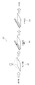
- FIG. 7 is a side view schematically showing a printing apparatus that executes the printing process.
- the printing apparatus 403 includes a plurality of discharge ports arranged one-dimensionally in the X-axis direction in the drawing, and the raw material liquid 200 is added while relatively moving the discharge ports and the substrate 100. Appropriate application between the banks 101 is performed.
- the foreign matter A does not absorb the raw material liquid 200, and the bank containing the foreign matter A exists.
- the amount of the raw material liquid 200 applied during 101 and the amount of the raw material liquid 200 containing the organic EL material that contributes to light emission are substantially the same.
- the thickness of the organic EL material obtained by drying the raw material liquid 200 and fixing it to the substrate 100 in the next process is almost the same regardless of the presence or absence of the foreign matter A.
- the organic EL display panel 300 including an inhibiting resin that covers or surrounds the foreign matter A between the banks 101.
- the organic EL display panel 300 can suppress the generation of the light emitting pixels 102 having abnormally high luminance.
- FIG. 8 is a perspective view schematically showing the substrate after the resin application step in Modification 1 of Embodiment 1.
- the inhibition resin 299 is not applied directly to the foreign material A, but can be used as long as the foreign material A can prevent the foreign material A from absorbing the raw material liquid 200. Alternatively, the inhibition resin 299 may be applied.
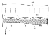
- FIG. 9 is a side view schematically illustrating a printing apparatus that executes a printing process according to the second modification of the first embodiment.
- the amount of the raw material liquid 200 applied between the banks 101 to which the inhibition resin 299 is applied is set to the amount of the raw material liquid 200 to be applied if no foreign matter A exists. It may be less than the amount. In this case, the same amount as the amount of the inhibition resin 299 applied by the resin application device 402 in the resin application step (S103) may be reduced. Furthermore, the application amount of the raw material liquid 200 may be reduced based on the amount of the inhibition resin 299 applied by the resin application device 402 and the size information generated by the detection device 401.
- the amount of the raw material liquid 200 to be applied can be adjusted corresponding to the area of the light emitting pixel 102 reduced by the foreign matter A and the applied inhibition resin 299, and the raw material liquid 200 is dried in the next step. It becomes possible to accurately adjust the thickness of the organic EL material fixed on the substrate 100.
- the second modification is particularly effective when the size of the foreign matter A is large.
- FIG. 10 is a diagram schematically illustrating an organic EL display panel manufacturing system according to the second embodiment.
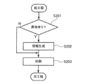
- the manufacturing system 400 includes a detection device 401 and a printing device 403.
- FIG. 11 is a flowchart showing a method of manufacturing the organic EL display panel according to the second embodiment.
- the foreign substance A present on the surface of the substrate 100 on the bank 101 side is detected by using the detection device 401 for the substrate 100 provided with the plurality of banks 101 in the previous process (S201: detection process). ).
- the detection device 401 When the foreign matter A is detected in the detection step (S201) (S201, Y), the detection device 401 generates position information indicating the position of the foreign matter A with respect to the substrate 100 (S202: information generation step). In the case of the present embodiment, the detection device 401 also generates size information indicating the size of the foreign object A in the information generation step S202.
- the printing apparatus 403 includes a raw material liquid 200 containing an organic EL material between the banks 101 of the substrate 100 provided with the plurality of banks 101. Is applied (S104: printing step).
- the printing apparatus 403 uses the amount of the raw material liquid 200 applied between the banks 101 where the foreign matter A exists based on the position information. Then, the amount of the raw material liquid 200 to be applied is made larger than the amount of the raw material liquid 200 to be applied, that is, the amount of the raw material liquid 200 excluding the amount absorbed by the foreign matter A is set between the other banks 101. Same as the amount applied.
- the coating amount of the raw material liquid 200 may be increased based on the size information generated by the detection device 401.
- the raw material liquid 200 for applying the organic EL material that is absorbed by the foreign matter A and does not contribute to light emission Is substantially equal to the amount of the raw material liquid 200 filled in the other portions.
- the thickness of the organic EL material obtained by drying the raw material liquid 200 and fixing it to the substrate 100 in the next process is almost the same regardless of the presence or absence of the foreign matter A.
- the same voltage is applied, it is possible to manufacture the organic EL display panel 300 in which the generation of the light emitting pixels 102 having an abnormally high luminance is suppressed.
- Embodiments 1 and 2 and modifications have been described as examples of the technology disclosed in the present application.
- the technology in the present disclosure is not limited to these, and can also be applied to embodiments in which changes, replacements, additions, omissions, and the like are appropriately performed.
- the organic EL display panel 300 is provided in a television.
- the organic EL display panel 300 may be used other than the television.
- the organic EL display panel 300 includes a monitor device that displays video input from the outside, digital signage used as an advertising medium, a portable terminal that accepts user operations via a touch panel, a tablet terminal, and a table-type organic display It may be realized as the EL display panel 300 or the like.
- the substrate 100 provided with the line bank has been described as an example.
- the banks provided on the substrate are not only the line bank, but the vertical bank 111 and the horizontal bank 112 have the same height, A substrate 100 or the like on which the raw material liquid 200 is applied to each light emitting pixel 102 may be used.
- the present disclosure is a manufacturing method of an organic EL display panel 300 that displays images, characters, and moving images, and a manufacturing system of the organic EL display panel 300, and is particularly applicable to a large organic EL display panel 300.
- the present disclosure is applicable to electronic devices such as a television, a monitor display, digital signage, a portable terminal, a tablet terminal, and a table-type organic EL display panel 300.
- Substrate 101 Bank 102 Light emitting pixel 111 Vertical bank 112 Horizontal bank 200 Raw material liquid 299 Inhibiting resin 300 Organic EL display panel 399 Television 400 Manufacturing system 401 Detection device 402 Resin coating device 403 Printing device 421 Head 422 Nozzle
Landscapes
- Engineering & Computer Science (AREA)
- Manufacturing & Machinery (AREA)
- Microelectronics & Electronic Packaging (AREA)
- Physics & Mathematics (AREA)
- Optics & Photonics (AREA)
- Electroluminescent Light Sources (AREA)
Abstract
Description
[有機EL表示パネルの概要]
有機EL表示パネル300は、例えば図3に示すように、映像や画像、文字などを表示する装置であり、図1に示すような基板100から製造される表示装置である。例えば、有機EL表示パネル300は、受信した放送波等から得られる映像を出力するテレビ399に組み込まれる。有機EL表示パネル300は、有機EL材料で発光層が構成された発光ダイオードである有機EL(Electro Luminescence)ダイオードを発光素子として備えている。本開示の場合、有機EL材料で発光層を形成する方法は印刷法であり、特に本実施の形態では、各発光色に対応した有機EL材料が含まれる複数種類(本実施の形態では3種類)の原料液200を所定のバンク101の間にそれぞれ吐出して原料液200を充填する印刷方法が採用される。
図4は、有機EL表示パネルの製造システムを模式的に示す図である。
次に、有機EL表示パネル300の製造方法について説明する。
図8は、実施の形態1の変形例1における樹脂塗布工程後の基板を模式的に示す斜視図である。
図9は、実施の形態1の変形例2における印刷工程を実行する印刷装置を模式的に示す側面図である。
[有機EL表示パネルの製造システム]
図10は、実施の形態2にかかる有機EL表示パネルの製造システムを模式的に示す図である。
次に、実施の形態2にかかる有機EL表示パネル300の製造方法について説明する。
以上のように、本出願において開示する技術の例示として、実施の形態1、2および、変形例を説明した。しかしながら、本開示における技術は、これらに限定されず、適宜、変更、置き換え、付加、省略などを行った実施の形態にも適用可能である。また、上記実施の形態1や変形例で説明した各構成要素を組み合わせて、新たな実施の形態とすることも可能である。
101 バンク
102 発光画素
111 縦バンク
112 横バンク
200 原料液
299 阻害樹脂
300 有機EL表示パネル
399 テレビ
400 製造システム
401 検出装置
402 樹脂塗布装置
403 印刷装置
421 ヘッド
422 ノズル
Claims (6)
- 複数のバンクが設けられた基板の前記バンクの間に有機EL材料を含む原料液を塗布する印刷工程を経て有機EL表示パネルを製造する方法であって、
前記印刷工程の前に、
前記基板の前記バンク側の表面に存在する異物を検出する検出工程と、
前記異物を検出した場合に前記基板に対する前記異物の位置を示す位置情報を生成する情報生成工程と、
前記位置情報に基づいて、前記異物、および、その周囲の少なくとも一方に前記異物が前記原料液を吸収することを阻害する阻害樹脂を塗布する樹脂塗布工程とを含む
有機EL表示パネルの製造方法。 - 前記印刷工程においては、
前記阻害樹脂が塗布された前記バンクの間に塗布する前記原料液の量を、前記異物が存在しなかったならば塗布する前記原料液の量よりも少なくする
請求項1に記載の有機EL表示パネルの製造方法。 - 前記検出工程において、
前記異物の大きさを示すサイズ情報を生成し、
前記印刷工程において、
前記阻害樹脂が塗布された前記バンクの間に塗布する前記原料液の量を、前記異物が存在しなかったならば塗布する前記原料液の量よりも前記サイズ情報に基づき少なくする
請求項2に記載の有機EL表示パネルの製造方法。 - 前記阻害樹脂は、前記原料液をはじく撥液性を備える
請求項1~3のいずれか1項に記載の有機EL表示パネルの製造方法。 - 複数のバンクが設けられた基板の前記バンクの間に有機EL材料を含む原料液を塗布する印刷工程を経て有機EL表示パネルを製造する方法であって、
前記印刷工程の前に、
前記基板の前記バンク側の表面に存在する異物を検出し、前記基板に対する前記異物の位置を示す位置情報を生成する検出工程を含み、
前記印刷工程においては、
前記位置情報に基づいて、前記異物が存在する前記バンクの間に塗布する前記原料液の量を、前記異物が存在しなかったならば塗布する前記原料液の量よりも多くする
有機EL表示パネルの製造方法。 - 複数のバンクが設けられた基板の前記バンク側の表面に存在する異物を検出し、前記基板に対する前記異物の位置を示す位置情報を生成する検出装置と、
前記位置情報に基づいて、前記異物、および、その周囲の少なくとも一方に前記異物が前記原料液を吸収することを阻害する阻害樹脂を塗布する樹脂塗布装置と、
前記基板の前記バンクの間に有機EL材料を含む原料液を塗布する印刷装置と
を備える有機EL表示パネルの製造システム。
Priority Applications (2)
| Application Number | Priority Date | Filing Date | Title |
|---|---|---|---|
| US14/906,984 US9548452B2 (en) | 2014-04-23 | 2015-04-17 | Method for manufacturing organic EL display panel and system for manufacturing organic EL display panel |
| JP2016514709A JPWO2015162891A1 (ja) | 2014-04-23 | 2015-04-17 | 有機el表示パネルの製造方法および有機el表示パネルの製造システム |
Applications Claiming Priority (2)
| Application Number | Priority Date | Filing Date | Title |
|---|---|---|---|
| JP2014-089668 | 2014-04-23 | ||
| JP2014089668 | 2014-04-23 |
Publications (1)
| Publication Number | Publication Date |
|---|---|
| WO2015162891A1 true WO2015162891A1 (ja) | 2015-10-29 |
Family
ID=54332070
Family Applications (1)
| Application Number | Title | Priority Date | Filing Date |
|---|---|---|---|
| PCT/JP2015/002124 Ceased WO2015162891A1 (ja) | 2014-04-23 | 2015-04-17 | 有機el表示パネルの製造方法および有機el表示パネルの製造システム |
Country Status (3)
| Country | Link |
|---|---|
| US (1) | US9548452B2 (ja) |
| JP (1) | JPWO2015162891A1 (ja) |
| WO (1) | WO2015162891A1 (ja) |
Cited By (1)
| Publication number | Priority date | Publication date | Assignee | Title |
|---|---|---|---|---|
| WO2019058528A1 (ja) * | 2017-09-22 | 2019-03-28 | シャープ株式会社 | 表示装置の製造方法 |
Citations (8)
| Publication number | Priority date | Publication date | Assignee | Title |
|---|---|---|---|---|
| JP2004253214A (ja) * | 2003-02-19 | 2004-09-09 | Sony Corp | 有機elデバイスの製造方法および有機elデバイス |
| JP2011048984A (ja) * | 2009-08-26 | 2011-03-10 | Toppan Printing Co Ltd | 有機el素子及びその製造方法並びにその製造に用いるリペアシート |
| JP2011108369A (ja) * | 2009-11-12 | 2011-06-02 | Hitachi High-Technologies Corp | 有機エレクトロルミネセンス表示装置の製造方法、有機エレクトロルミネセンス表示装置の修正装置、および、ニードル |
| JP2012230852A (ja) * | 2011-04-27 | 2012-11-22 | Seiko Epson Corp | 有機エレクトロルミネッセンス表示装置の製造方法、有機エレクトロルミネッセンス表示装置のリペア方法、および電子機器 |
| JP2012234647A (ja) * | 2011-04-28 | 2012-11-29 | Seiko Epson Corp | 有機エレクトロルミネッセンス表示装置の製造方法、有機エレクトロルミネッセンス表示装置のリペア方法、および電子機器 |
| JP2013016342A (ja) * | 2011-07-04 | 2013-01-24 | Seiko Epson Corp | 有機エレクトロルミネッセンス表示装置の製造方法、有機エレクトロルミネッセンス表示装置のリペア方法、および電子機器 |
| WO2013190841A1 (ja) * | 2012-06-21 | 2013-12-27 | パナソニック株式会社 | 被覆方法および有機el素子の製造方法 |
| JP2014002983A (ja) * | 2012-06-21 | 2014-01-09 | Panasonic Corp | 有機el表示装置およびその製造方法 |
Family Cites Families (5)
| Publication number | Priority date | Publication date | Assignee | Title |
|---|---|---|---|---|
| JP4507817B2 (ja) | 2004-10-18 | 2010-07-21 | セイコーエプソン株式会社 | 液滴吐出による表示基板の製造方法、表示基板、及び表示装置の製造方法、表示装置、並びに電子機器 |
| JP4636921B2 (ja) * | 2005-03-30 | 2011-02-23 | セイコーエプソン株式会社 | 表示装置の製造方法、表示装置および電子機器 |
| JP2009139678A (ja) * | 2007-12-07 | 2009-06-25 | Seiko Epson Corp | 発光装置及び電子機器並びに成膜方法 |
| JP5678740B2 (ja) * | 2011-03-11 | 2015-03-04 | ソニー株式会社 | 有機el表示装置および電子機器 |
| US9246036B2 (en) * | 2012-08-20 | 2016-01-26 | Universal Display Corporation | Thin film deposition |
-
2015
- 2015-04-17 WO PCT/JP2015/002124 patent/WO2015162891A1/ja not_active Ceased
- 2015-04-17 US US14/906,984 patent/US9548452B2/en active Active
- 2015-04-17 JP JP2016514709A patent/JPWO2015162891A1/ja active Pending
Patent Citations (8)
| Publication number | Priority date | Publication date | Assignee | Title |
|---|---|---|---|---|
| JP2004253214A (ja) * | 2003-02-19 | 2004-09-09 | Sony Corp | 有機elデバイスの製造方法および有機elデバイス |
| JP2011048984A (ja) * | 2009-08-26 | 2011-03-10 | Toppan Printing Co Ltd | 有機el素子及びその製造方法並びにその製造に用いるリペアシート |
| JP2011108369A (ja) * | 2009-11-12 | 2011-06-02 | Hitachi High-Technologies Corp | 有機エレクトロルミネセンス表示装置の製造方法、有機エレクトロルミネセンス表示装置の修正装置、および、ニードル |
| JP2012230852A (ja) * | 2011-04-27 | 2012-11-22 | Seiko Epson Corp | 有機エレクトロルミネッセンス表示装置の製造方法、有機エレクトロルミネッセンス表示装置のリペア方法、および電子機器 |
| JP2012234647A (ja) * | 2011-04-28 | 2012-11-29 | Seiko Epson Corp | 有機エレクトロルミネッセンス表示装置の製造方法、有機エレクトロルミネッセンス表示装置のリペア方法、および電子機器 |
| JP2013016342A (ja) * | 2011-07-04 | 2013-01-24 | Seiko Epson Corp | 有機エレクトロルミネッセンス表示装置の製造方法、有機エレクトロルミネッセンス表示装置のリペア方法、および電子機器 |
| WO2013190841A1 (ja) * | 2012-06-21 | 2013-12-27 | パナソニック株式会社 | 被覆方法および有機el素子の製造方法 |
| JP2014002983A (ja) * | 2012-06-21 | 2014-01-09 | Panasonic Corp | 有機el表示装置およびその製造方法 |
Cited By (2)
| Publication number | Priority date | Publication date | Assignee | Title |
|---|---|---|---|---|
| WO2019058528A1 (ja) * | 2017-09-22 | 2019-03-28 | シャープ株式会社 | 表示装置の製造方法 |
| US10573853B2 (en) | 2017-09-22 | 2020-02-25 | Sharp Kabushiki Kaisha | Method of manufacturing display device |
Also Published As
| Publication number | Publication date |
|---|---|
| US20160172592A1 (en) | 2016-06-16 |
| US9548452B2 (en) | 2017-01-17 |
| JPWO2015162891A1 (ja) | 2017-04-13 |
Similar Documents
| Publication | Publication Date | Title |
|---|---|---|
| US9653526B2 (en) | Pixel defining layer and manufacturing method thereof, display panel and display device | |
| KR102052331B1 (ko) | 잉크젯 프린트 헤드, 이를 포함한 유기 발광 표시 장치의 제조 장치 및 그 방법 | |
| US10446622B2 (en) | OLED pixel defining structure with at least two intercommunicated sub-pixel defining zones of same color, manufacturing method thereof and array substrate | |
| US9312486B2 (en) | Method for fabricating organic light emitting display device by predepositing a solvent to increase wettability and inkjet print device used therein | |
| KR101979181B1 (ko) | 고해상도 유기 발광 다이오드 장치 | |
| WO2017190585A1 (en) | Display substrate and method of fabricating display substrate | |
| US20140197396A1 (en) | High Resolution Organic Light-Emitting Diode Devices, Displays, and Related Method | |
| CN105045442B (zh) | 电极基板、显示装置、输入装置及电极基板的制造方法 | |
| US20140197385A1 (en) | High Resolution Organic Light-Emitting Diode Devices, Displays, and Related Methods | |
| US10333066B2 (en) | Pixel definition layer and manufacturing method thereof, display substrate and display device | |
| JP2015160153A (ja) | 塗布製品の量産方法 | |
| US9735215B2 (en) | Pixel demarcation layer, OLED and manufacturing method thereof as well as display device | |
| US10452186B2 (en) | Handwriting display device, and manufacturing method and controlling method for the same | |
| JP2014123489A (ja) | ノズル吐出量の補正方法、機能液の吐出方法、有機el装置の製造方法 | |
| JP4983300B2 (ja) | 液状体の吐出方法、カラーフィルタの製造方法、有機el素子の製造方法、電気光学装置の製造方法 | |
| JP4466115B2 (ja) | 有機エレクトロルミネッセンス装置、有機エレクトロルミネッセンス装置の製造方法、及び電子機器 | |
| WO2015162891A1 (ja) | 有機el表示パネルの製造方法および有機el表示パネルの製造システム | |
| JP2007206686A (ja) | カラーフィルタ製造方法 | |
| CN108511634A (zh) | 喷墨打印机及其打印方法 | |
| US8944564B2 (en) | Printing apparatus and method for manufacturing organic light emitting diode display | |
| JP2013045821A (ja) | インクジェット装置 | |
| JP5707019B2 (ja) | 電気光学装置および電子機器 | |
| US10014353B2 (en) | Substrate, display device having the same, and fabricating method thereof | |
| JP2007130605A (ja) | 描画方法、および電気光学装置の製造方法、電気光学装置、ならびに電子機器 | |
| WO2015174025A1 (ja) | 有機el表示パネルの製造方法および有機el表示パネルの製造システム |
Legal Events
| Date | Code | Title | Description |
|---|---|---|---|
| 121 | Ep: the epo has been informed by wipo that ep was designated in this application |
Ref document number: 15782574 Country of ref document: EP Kind code of ref document: A1 |
|
| WWE | Wipo information: entry into national phase |
Ref document number: 14906984 Country of ref document: US |
|
| ENP | Entry into the national phase |
Ref document number: 2016514709 Country of ref document: JP Kind code of ref document: A |
|
| NENP | Non-entry into the national phase |
Ref country code: DE |
|
| 122 | Ep: pct application non-entry in european phase |
Ref document number: 15782574 Country of ref document: EP Kind code of ref document: A1 |