WO2015156249A1 - 表示装置 - Google Patents
表示装置 Download PDFInfo
- Publication number
- WO2015156249A1 WO2015156249A1 PCT/JP2015/060744 JP2015060744W WO2015156249A1 WO 2015156249 A1 WO2015156249 A1 WO 2015156249A1 JP 2015060744 W JP2015060744 W JP 2015060744W WO 2015156249 A1 WO2015156249 A1 WO 2015156249A1
- Authority
- WO
- WIPO (PCT)
- Prior art keywords
- scanning
- wiring
- line
- semiconductor layer
- common wiring
- Prior art date
- Legal status (The legal status is an assumption and is not a legal conclusion. Google has not performed a legal analysis and makes no representation as to the accuracy of the status listed.)
- Ceased
Links
Images






Classifications
-
- H—ELECTRICITY
- H10—SEMICONDUCTOR DEVICES; ELECTRIC SOLID-STATE DEVICES NOT OTHERWISE PROVIDED FOR
- H10D—INORGANIC ELECTRIC SEMICONDUCTOR DEVICES
- H10D86/00—Integrated devices formed in or on insulating or conducting substrates, e.g. formed in silicon-on-insulator [SOI] substrates or on stainless steel or glass substrates
- H10D86/40—Integrated devices formed in or on insulating or conducting substrates, e.g. formed in silicon-on-insulator [SOI] substrates or on stainless steel or glass substrates characterised by multiple TFTs
- H10D86/441—Interconnections, e.g. scanning lines
-
- G—PHYSICS
- G02—OPTICS
- G02F—OPTICAL DEVICES OR ARRANGEMENTS FOR THE CONTROL OF LIGHT BY MODIFICATION OF THE OPTICAL PROPERTIES OF THE MEDIA OF THE ELEMENTS INVOLVED THEREIN; NON-LINEAR OPTICS; FREQUENCY-CHANGING OF LIGHT; OPTICAL LOGIC ELEMENTS; OPTICAL ANALOGUE/DIGITAL CONVERTERS
- G02F1/00—Devices or arrangements for the control of the intensity, colour, phase, polarisation or direction of light arriving from an independent light source, e.g. switching, gating or modulating; Non-linear optics
- G02F1/01—Devices or arrangements for the control of the intensity, colour, phase, polarisation or direction of light arriving from an independent light source, e.g. switching, gating or modulating; Non-linear optics for the control of the intensity, phase, polarisation or colour
- G02F1/13—Devices or arrangements for the control of the intensity, colour, phase, polarisation or direction of light arriving from an independent light source, e.g. switching, gating or modulating; Non-linear optics for the control of the intensity, phase, polarisation or colour based on liquid crystals, e.g. single liquid crystal display cells
- G02F1/133—Constructional arrangements; Operation of liquid crystal cells; Circuit arrangements
- G02F1/136—Liquid crystal cells structurally associated with a semi-conducting layer or substrate, e.g. cells forming part of an integrated circuit
- G02F1/1362—Active matrix addressed cells
- G02F1/136204—Arrangements to prevent high voltage or static electricity failures
-
- G—PHYSICS
- G02—OPTICS
- G02F—OPTICAL DEVICES OR ARRANGEMENTS FOR THE CONTROL OF LIGHT BY MODIFICATION OF THE OPTICAL PROPERTIES OF THE MEDIA OF THE ELEMENTS INVOLVED THEREIN; NON-LINEAR OPTICS; FREQUENCY-CHANGING OF LIGHT; OPTICAL LOGIC ELEMENTS; OPTICAL ANALOGUE/DIGITAL CONVERTERS
- G02F1/00—Devices or arrangements for the control of the intensity, colour, phase, polarisation or direction of light arriving from an independent light source, e.g. switching, gating or modulating; Non-linear optics
- G02F1/01—Devices or arrangements for the control of the intensity, colour, phase, polarisation or direction of light arriving from an independent light source, e.g. switching, gating or modulating; Non-linear optics for the control of the intensity, phase, polarisation or colour
- G02F1/13—Devices or arrangements for the control of the intensity, colour, phase, polarisation or direction of light arriving from an independent light source, e.g. switching, gating or modulating; Non-linear optics for the control of the intensity, phase, polarisation or colour based on liquid crystals, e.g. single liquid crystal display cells
- G02F1/133—Constructional arrangements; Operation of liquid crystal cells; Circuit arrangements
- G02F1/136—Liquid crystal cells structurally associated with a semi-conducting layer or substrate, e.g. cells forming part of an integrated circuit
- G02F1/1362—Active matrix addressed cells
- G02F1/136286—Wiring, e.g. gate line, drain line
-
- G—PHYSICS
- G02—OPTICS
- G02F—OPTICAL DEVICES OR ARRANGEMENTS FOR THE CONTROL OF LIGHT BY MODIFICATION OF THE OPTICAL PROPERTIES OF THE MEDIA OF THE ELEMENTS INVOLVED THEREIN; NON-LINEAR OPTICS; FREQUENCY-CHANGING OF LIGHT; OPTICAL LOGIC ELEMENTS; OPTICAL ANALOGUE/DIGITAL CONVERTERS
- G02F1/00—Devices or arrangements for the control of the intensity, colour, phase, polarisation or direction of light arriving from an independent light source, e.g. switching, gating or modulating; Non-linear optics
- G02F1/01—Devices or arrangements for the control of the intensity, colour, phase, polarisation or direction of light arriving from an independent light source, e.g. switching, gating or modulating; Non-linear optics for the control of the intensity, phase, polarisation or colour
- G02F1/13—Devices or arrangements for the control of the intensity, colour, phase, polarisation or direction of light arriving from an independent light source, e.g. switching, gating or modulating; Non-linear optics for the control of the intensity, phase, polarisation or colour based on liquid crystals, e.g. single liquid crystal display cells
- G02F1/133—Constructional arrangements; Operation of liquid crystal cells; Circuit arrangements
- G02F1/136—Liquid crystal cells structurally associated with a semi-conducting layer or substrate, e.g. cells forming part of an integrated circuit
- G02F1/1362—Active matrix addressed cells
- G02F1/1368—Active matrix addressed cells in which the switching element is a three-electrode device
-
- H—ELECTRICITY
- H10—SEMICONDUCTOR DEVICES; ELECTRIC SOLID-STATE DEVICES NOT OTHERWISE PROVIDED FOR
- H10D—INORGANIC ELECTRIC SEMICONDUCTOR DEVICES
- H10D30/00—Field-effect transistors [FET]
- H10D30/60—Insulated-gate field-effect transistors [IGFET]
- H10D30/67—Thin-film transistors [TFT]
-
- H—ELECTRICITY
- H10—SEMICONDUCTOR DEVICES; ELECTRIC SOLID-STATE DEVICES NOT OTHERWISE PROVIDED FOR
- H10D—INORGANIC ELECTRIC SEMICONDUCTOR DEVICES
- H10D64/00—Electrodes of devices having potential barriers
- H10D64/01—Manufacture or treatment
- H10D64/011—Manufacture or treatment of electrodes ohmically coupled to a semiconductor
-
- H—ELECTRICITY
- H10—SEMICONDUCTOR DEVICES; ELECTRIC SOLID-STATE DEVICES NOT OTHERWISE PROVIDED FOR
- H10D—INORGANIC ELECTRIC SEMICONDUCTOR DEVICES
- H10D86/00—Integrated devices formed in or on insulating or conducting substrates, e.g. formed in silicon-on-insulator [SOI] substrates or on stainless steel or glass substrates
- H10D86/40—Integrated devices formed in or on insulating or conducting substrates, e.g. formed in silicon-on-insulator [SOI] substrates or on stainless steel or glass substrates characterised by multiple TFTs
- H10D86/481—Integrated devices formed in or on insulating or conducting substrates, e.g. formed in silicon-on-insulator [SOI] substrates or on stainless steel or glass substrates characterised by multiple TFTs integrated with passive devices, e.g. auxiliary capacitors
-
- H—ELECTRICITY
- H10—SEMICONDUCTOR DEVICES; ELECTRIC SOLID-STATE DEVICES NOT OTHERWISE PROVIDED FOR
- H10D—INORGANIC ELECTRIC SEMICONDUCTOR DEVICES
- H10D86/00—Integrated devices formed in or on insulating or conducting substrates, e.g. formed in silicon-on-insulator [SOI] substrates or on stainless steel or glass substrates
- H10D86/40—Integrated devices formed in or on insulating or conducting substrates, e.g. formed in silicon-on-insulator [SOI] substrates or on stainless steel or glass substrates characterised by multiple TFTs
- H10D86/60—Integrated devices formed in or on insulating or conducting substrates, e.g. formed in silicon-on-insulator [SOI] substrates or on stainless steel or glass substrates characterised by multiple TFTs wherein the TFTs are in active matrices
-
- H—ELECTRICITY
- H10—SEMICONDUCTOR DEVICES; ELECTRIC SOLID-STATE DEVICES NOT OTHERWISE PROVIDED FOR
- H10D—INORGANIC ELECTRIC SEMICONDUCTOR DEVICES
- H10D89/00—Aspects of integrated devices not covered by groups H10D84/00 - H10D88/00
- H10D89/60—Integrated devices comprising arrangements for electrical or thermal protection, e.g. protection circuits against electrostatic discharge [ESD]
- H10D89/601—Integrated devices comprising arrangements for electrical or thermal protection, e.g. protection circuits against electrostatic discharge [ESD] for devices having insulated gate electrodes, e.g. for IGFETs or IGBTs
- H10D89/611—Integrated devices comprising arrangements for electrical or thermal protection, e.g. protection circuits against electrostatic discharge [ESD] for devices having insulated gate electrodes, e.g. for IGFETs or IGBTs using diodes as protective elements
-
- H—ELECTRICITY
- H10—SEMICONDUCTOR DEVICES; ELECTRIC SOLID-STATE DEVICES NOT OTHERWISE PROVIDED FOR
- H10D—INORGANIC ELECTRIC SEMICONDUCTOR DEVICES
- H10D89/00—Aspects of integrated devices not covered by groups H10D84/00 - H10D88/00
- H10D89/60—Integrated devices comprising arrangements for electrical or thermal protection, e.g. protection circuits against electrostatic discharge [ESD]
- H10D89/601—Integrated devices comprising arrangements for electrical or thermal protection, e.g. protection circuits against electrostatic discharge [ESD] for devices having insulated gate electrodes, e.g. for IGFETs or IGBTs
- H10D89/811—Integrated devices comprising arrangements for electrical or thermal protection, e.g. protection circuits against electrostatic discharge [ESD] for devices having insulated gate electrodes, e.g. for IGFETs or IGBTs using FETs as protective elements
-
- H—ELECTRICITY
- H10—SEMICONDUCTOR DEVICES; ELECTRIC SOLID-STATE DEVICES NOT OTHERWISE PROVIDED FOR
- H10K—ORGANIC ELECTRIC SOLID-STATE DEVICES
- H10K59/00—Integrated devices, or assemblies of multiple devices, comprising at least one organic light-emitting element covered by group H10K50/00
- H10K59/10—OLED displays
- H10K59/12—Active-matrix OLED [AMOLED] displays
-
- H—ELECTRICITY
- H10—SEMICONDUCTOR DEVICES; ELECTRIC SOLID-STATE DEVICES NOT OTHERWISE PROVIDED FOR
- H10K—ORGANIC ELECTRIC SOLID-STATE DEVICES
- H10K59/00—Integrated devices, or assemblies of multiple devices, comprising at least one organic light-emitting element covered by group H10K50/00
- H10K59/10—OLED displays
- H10K59/12—Active-matrix OLED [AMOLED] displays
- H10K59/131—Interconnections, e.g. wiring lines or terminals
-
- H—ELECTRICITY
- H10—SEMICONDUCTOR DEVICES; ELECTRIC SOLID-STATE DEVICES NOT OTHERWISE PROVIDED FOR
- H10W—GENERIC PACKAGES, INTERCONNECTIONS, CONNECTORS OR OTHER CONSTRUCTIONAL DETAILS OF DEVICES COVERED BY CLASS H10
- H10W20/00—Interconnections in chips, wafers or substrates
- H10W20/40—Interconnections external to wafers or substrates, e.g. back-end-of-line [BEOL] metallisations or vias connecting to gate electrodes
- H10W20/495—Capacitive arrangements or effects of, or between wiring layers
- H10W20/496—Capacitor integral with wiring layers
Definitions
- the present invention relates to a display device.
- This application claims priority based on Japanese Patent Application No. 2014-079514 filed in Japan on April 8, 2014, the contents of which are incorporated herein by reference.
- a display device provided with an active matrix substrate is conventionally known.
- contact, friction, peeling, etc. between the glass substrate and other members frequently occur. Therefore, accumulation of electric charges on a semiconductor layer, a scanning line, a signal line, and the like on the glass substrate is unavoidable, and there are cases where a thin film transistor (hereinafter referred to as TFT) and wiring are destroyed due to static electricity.
- TFT thin film transistor
- Patent Document 1 discloses a method for manufacturing an active matrix type liquid crystal display device.
- This Patent Document 1 describes a surge protection circuit for preventing element destruction due to surge voltage application in a liquid crystal panel.
- a surge protection circuit specifically, a semiconductor layer, a scanning line, and a scanning line formed on a transparent substrate until a signal line, a signal common wiring, and the like are formed.
- Common wiring and the like are independent in an island shape. For this reason, there is no escape route for charges, and charges accumulate in these. This accumulated charge may cause a phenomenon of destruction due to static electricity.
- the phenomenon of breakdown caused by static electricity generated between the scanning line and its adjacent wiring, for example, the scanning common wiring due to the accumulation of electric charges in the scanning line occupies many of the factors that reduce the manufacturing yield of the liquid crystal display device.
- One aspect of the present invention has been made to solve the above-described problem, and is a phenomenon of breakdown caused by static electricity generated until a protection circuit is formed, particularly between a scanning line and an adjacent wiring. Another object is to realize a structure of a display device that can suppress a breakdown phenomenon caused by static electricity.
- a display device includes a plurality of scanning lines and a plurality of signal lines intersecting each other, and a plurality of scanning lines partitioned by the plurality of scanning lines and the plurality of signal lines.
- a plurality of pixel circuit TFTs provided in a pixel; a scanning common wiring that electrically connects the plurality of scanning lines; and an electrical connection between each of the scanning common wiring and the plurality of scanning lines.
- a plurality of protective elements to be connected, and at least some of the plurality of connection wirings that electrically connect the scanning common wiring and the plurality of protective elements are configured by wiring in the same layer as the signal lines
- the plurality of pixel circuit semiconductor layers constituting the plurality of pixel circuit TFTs and each of the plurality of scanning lines overlap in a plane, and a plurality of semiconductor layers in the same layer as the pixel circuit semiconductor layer And a common arrangement crossing the plurality of scanning lines. Doo overlap in plan view, the area of overlap between the scanning lines and the semiconductor layer for the plurality of pixel circuits, the area of overlap between the common wiring and the plurality of semiconductor layers, but approximately equal.
- the common wiring may be the scanning common wiring.
- a part of the plurality of connection wirings includes a wiring in the same layer as the signal line, and the remaining connection wirings of the plurality of connection wirings Is constituted by wiring integrated with the scanning common wiring, and the plurality of semiconductor layers are a plurality of first semiconductor layers constituting the plurality of protection elements, and the plurality of pixel circuit semiconductor layers and the scanning lines
- the area of the overlapping portion between and the area of the overlapping portion between the plurality of first semiconductor layers and the scanning common wiring may be substantially equal.
- the plurality of semiconductor layers are a plurality of second semiconductor layers that are the same layer as the semiconductor layer for pixel circuit and the first semiconductor layer for protection element, and the plurality of connections. All of the wirings are composed of wirings in the same layer as the signal lines, further comprising relay wirings in the same layer as the signal lines, wherein at least a part of the second semiconductor layer and at least a part of the relay wirings are A plurality of pixel circuit semiconductor layers and the scanning line; and an overlapping area between the plurality of second semiconductor layers and the scanning common wiring.
- the scanning common wiring and the second semiconductor layer may be electrically connected via the relay wiring.
- the first end of the second semiconductor layer overlaps the scan common wiring in a plane, and the second end of the second semiconductor layer is common to the scan. You may protrude to the one side of the width direction of wiring.
- a central portion of the second semiconductor layer overlaps with the scanning common wiring in a plane, and both end portions of the second semiconductor layer are on both sides in the width direction of the scanning common wiring. You may stick out.
- the display device may further include an auxiliary capacitance line constituting an auxiliary capacitance, and the common wiring may be the auxiliary capacitance line.
- the plurality of semiconductor layers are a plurality of second semiconductor layers that are the same layer as the semiconductor layer for pixel circuit and the first semiconductor layer for protection element, and the plurality of connections. All of the wirings are composed of wirings in the same layer as the signal lines, further comprising relay wirings in the same layer as the signal lines, wherein at least a part of the second semiconductor layer and at least a part of the relay wirings are An area of the overlapping portion of the plurality of pixel circuit semiconductor layers and the scanning line, and an area of an overlapping portion of the plurality of second semiconductor layers and the auxiliary capacitance line are planarly overlapped with the storage capacitor line.
- the storage capacitor line and the second semiconductor layer may be electrically connected to each other via the relay wiring.
- one second semiconductor layer is provided for each pixel column, and the first end of the second semiconductor layer is planar with the storage capacitor line.
- the second end portion of the second semiconductor layer may protrude to one side in the width direction of the storage capacitor line.
- two second semiconductor layers are provided for each pixel column, and the first end of each of the two second semiconductor layers is the auxiliary capacitor.
- the second end of each of the two second semiconductor layers may protrude from both sides in the width direction of the storage capacitor line in a plane overlapping with the line.
- the present invention it is possible to suppress a breakdown phenomenon due to static electricity generated until a protection circuit is formed, particularly a breakdown phenomenon due to static electricity generated between a scanning line and its adjacent wiring. A display device is obtained.
- FIG. 4 is a first cross-sectional view taken along the line I-II in FIG. 3.
- FIG. 4 is a second cross-sectional view taken along the line II of FIG.
- FIG. 6 is a sectional view taken along line III-IV in FIG. 5. It is a top view of the active matrix substrate which shows the layout of the protection circuit of 2nd Embodiment.
- FIG. 8 is a sectional view taken along line V-VI in FIG. 7. It is a top view of the active matrix substrate which shows the layout of the protection circuit of 3rd Embodiment.
- FIG. 10 is a cross-sectional view taken along line VII-VIII in FIG. 9. It is a top view of the active matrix substrate which shows the layout of the protection circuit of 4th Embodiment.
- FIG. 12 is a sectional view taken along line IX-X in FIG. 11. It is a top view of the active matrix substrate which shows the layout of the protection circuit of 5th Embodiment. It is sectional drawing which follows the XI-XII line
- FIG. 1 is a perspective view of an active matrix liquid crystal display device.
- the liquid crystal display device 50 includes, for example, an active matrix substrate 100 and a counter substrate 150 provided so as to face each other, and a liquid crystal layer sandwiched between the active matrix substrate 100 and the counter substrate 150. (Not shown).
- the liquid crystal display device 50 is provided with a display area 1 for displaying an image and a frame area 2 surrounding the display area 1.
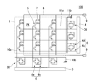
- FIG. 2 is a circuit configuration diagram of the liquid crystal display device 50.
- the active matrix substrate 100 includes, for example, a plurality of scanning lines 10a provided so as to extend in parallel to each other in the rectangular display region 1, and are parallel to each other in a direction orthogonal to the scanning lines 10a. And a plurality of signal lines 11a provided so as to extend in the direction.
- a pixel PX is formed in an area surrounded by adjacent scanning lines 10a and adjacent signal lines 11a. Inside the pixel PX, an auxiliary capacitor 7 and a pixel TFT 5 for switching are provided. The auxiliary capacitor 7 is connected to the terminal 9 through the auxiliary capacitor line 8. When the liquid crystal display device 50 is driven, a voltage is applied to one electrode of the auxiliary capacitor 7 from the outside through the terminal 9 and the auxiliary capacitor line 8.
- a scanning drive circuit 3 is arranged outside the display area 1 (lower side in FIG. 2).
- a signal drive circuit 4 is arranged outside the display area 1 (on the right side in FIG. 2).
- the scanning drive circuit 3 is directly formed on the active matrix substrate 100.
- the signal drive circuit 4 is incorporated in an IC driver 60 mounted on the active matrix substrate 100.
- the active matrix substrate 100 includes a protection circuit 30 described below.
- the scanning common wiring 10b is a wiring that electrically connects the plurality of scanning lines 10a.
- the signal common wiring 11b is a wiring that electrically connects the plurality of signal lines 11a. Protection diodes 6 are formed between the scanning line 10a and the scanning common wiring 10b and between the signal line 11a and the signal common wiring 11b, respectively. One end of the scanning common line 10b and one end of the signal common line 11b are each connected to ground.
- the “protection diode 6” in the present embodiment corresponds to a “protection element” in the claims.
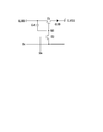
- the protective diode 6 is formed by short-circuiting the gates of the protective TFTs 6a, 6b, 6c, and 6d manufactured by the same process as the pixel TFT 5 formed in the display region 1 with its own drain or source.
- the gate of the protection TFT 6a is connected to the scanning line 10a
- the gate of the protection TFT 6c is connected to the signal line 11a.
- the gate of the protection TFT 6b is connected to the scanning common line 10b
- the gate of the protection TFT 6d is connected to the signal common line 11b.
- the reason why the protection TFTs 6a, 6b, 6c and 6d having different directions are arranged between the scanning line 10a and the scanning common wiring 10b or between the signal line 11a and the signal common wiring 11b is that the static electricity is a positive voltage. This is because it is necessary to cope with both the case of the negative voltage and the case of the negative voltage.
- FIG. 3 is a plan view showing a layout of the protective TFTs 6a and 6b of the comparative example.
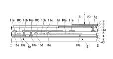
- 4A is a cross-sectional view taken along the line II-II of FIG. 3 and 4A illustrate a top gate TFT which is a TFT of a type in which the scanning line 10a is disposed on the upper side of the semiconductor layer 13a (upward in FIG. 4A).
- a method for manufacturing the active matrix substrate 100 will be described with reference to FIGS. 3 and 4A.
- a silicon nitride film, a silicon oxide film, or a laminated film thereof is formed with a thickness of about 50 nm by, for example, a CVD (Chemical Vapor Deposition) method.
- a CVD Chemical Vapor Deposition
- an intrinsic amorphous silicon film with a thickness of about 50 nm is formed on the entire substrate on which the base film 12 has been formed, for example, by CVD.
- the intrinsic amorphous silicon film is polycrystallized by annealing such as laser light irradiation to form a polysilicon film.
- a semiconductor layer 13a and the like are formed by performing a photolithography process, an etching process, and a resist peeling process on the polysilicon film.
- an inorganic insulating film such as a silicon nitride film, a silicon oxide film, or a laminated film thereof is formed with a thickness of about 100 nm on the entire substrate on which the semiconductor layer 13a and the like are formed, for example, by a CVD method. 14 is formed. Further, a metal film such as a tungsten film is formed with a thickness of about 300 nm on the entire substrate on which the gate insulating film 14 has been formed, for example, by sputtering. Thereafter, a photolithography process, an etching process, and a resist stripping process are performed on the metal film, thereby forming the scanning line 10a, the scanning common wiring 10b, the other gate wiring 10c, and the like.
- a channel region, a source region, and a drain region are formed in the semiconductor layer 13a and the like by implanting impurities such as phosphorus into the semiconductor layer 13a and the like on the substrate using the scanning line 10a as a mask.
- an inorganic insulating film such as a silicon nitride film, a silicon oxide film, or a stacked film thereof is formed on the entire substrate on which the channel region, the source region, and the drain region of the semiconductor layer 13a are formed by a CVD method, for example. nm].
- an interlayer insulating film having contact holes 16a, 16b, 16c, 16d, 16e, etc. is obtained by subjecting the inorganic insulating film and the underlying gate insulating film 14 to a photolithography process, an etching process, and a resist stripping process. 15 is formed.
- a metal film such as an aluminum film is formed with a thickness of about 350 nm on the entire substrate on which the interlayer insulating film 15 has been formed, for example, by sputtering.
- a photolithography process, an etching process, and a resist stripping process are performed on the metal film, thereby forming a signal line 11a, a signal common line 11b, other source lines 11c, an auxiliary capacitance line 11d, and the like.
- the scanning drive circuit 3, the pixel TFT 5, and the protection circuit 30 including the protection TFTs 6a, 6b, 6c, and 6d are formed.
- an acrylic photosensitive resin film with a thickness of about 2 ⁇ m is applied to the entire substrate on which the signal lines 11a and the like are formed, for example, by spin coating or slit coating. Thereafter, the coating film is pre-baked, exposed, developed and post-baked to form a protective insulating film 17 having contact holes 16f and the like.
- a transparent conductive film such as an ITO (Indium Tin Oxide) film is formed on the entire substrate on which the protective insulating film 17 has been formed to a thickness of about 100 nm, for example, by sputtering.
- the common electrode 18 and a part of the auxiliary capacitor 7 are formed by performing a photolithography process, an etching process, and a resist stripping process on the transparent conductive film.
- an inorganic insulating film such as a silicon nitride film, a silicon oxide film, or a laminated film thereof is formed with a thickness of about 200 nm on the entire substrate on which the common electrode 18 is formed, for example, by a CVD method.
- an interlayer insulating film 19 having contact holes 16g and the like is formed by performing photolithography processing, etching processing, and resist stripping processing on the inorganic insulating film.
- a transparent conductive film such as an ITO film is formed with a thickness of about 100 nm on the entire substrate on which the interlayer insulating film 19 has been formed, for example, by sputtering.
- a part of the pixel electrode 20 and the auxiliary capacitor 7 is formed by performing a photolithography process, an etching process, and a resist stripping process on the transparent conductive film.
- a polyimide resin film is applied to the entire substrate on which the pixel electrodes 20 and the like are formed by, for example, a spin coating method, a slit coating method, or a printing method, and then the coating film is baked and rubbed. As a result, an alignment film (not shown) is formed.
- the active matrix substrate 100 can be manufactured.
- a photosensitive resin colored in black is applied to the entire transparent substrate such as a glass substrate by, for example, a spin coating method or a slit coating method. Thereafter, the coating film is exposed and developed to form a black matrix having a thickness of about 1 ⁇ m.
- a photosensitive resin colored in red, green, or blue is applied to the entire substrate on which the black matrix is formed, for example, by spin coating or slit coating. Thereafter, the coated film is exposed and developed to form a colored layer (for example, a red layer) of a selected color with a thickness of about 1 ⁇ m to 3 ⁇ m. The same process is repeated for the other two colors to form other two colored layers (for example, a green layer and a blue layer) with a thickness of about 1 ⁇ m to 3 ⁇ m.
- an acrylic photosensitive resin film with a thickness of about 4 ⁇ m is applied to the entire substrate on which the colored layer has been formed, for example, by spin coating or slit coating. Thereafter, pre-baking, exposure, development, and post-baking are performed on the coating film, thereby forming a photo spacer for holding a gap between the active matrix substrate 100 and the counter substrate 150.
- a polyimide-based resin film is applied to the entire substrate on which the photospacers are formed by, for example, spin coating, slit coating, or printing. Thereafter, an alignment film is formed by baking and rubbing the coating film.
- the counter substrate 150 can be manufactured.
- a sealing material made of a UV (ultraviolet) curing and thermosetting resin or the like is printed in a frame shape on the surface of the counter substrate 150 manufactured in the above counter substrate manufacturing process. Thereafter, a liquid crystal material is dropped inside the sealing material. Subsequently, the counter substrate 150 onto which the liquid crystal material is dropped and the active matrix substrate 100 manufactured in the above active matrix substrate manufacturing process are bonded together in a reduced pressure atmosphere, and then released to atmospheric pressure. Further, after the sealing material is irradiated with UV light in the bonded state, the sealing material is cured by heating.
- the base material is divided by dicing, and unnecessary portions of the active matrix substrate 100 and the counter substrate 150 are removed.
- the active matrix liquid crystal display device 50 shown in FIG. 1 can be manufactured.
- the protection circuit 30 of the comparative example as shown in FIG. 3 it is transparent until the protection circuit 30 is formed, specifically, until the signal line 11a, the signal common wiring 11b, and the like are formed.
- the semiconductor layer 13a, the scanning line 10a, the scanning common wiring 10b, and the like formed on the substrate 40 are independent in an island shape. Therefore, there is no escape route for the generated charges, and charges accumulate in these. As a result, a breakdown phenomenon due to static electricity may occur.
- the accumulation of electric charges in the scanning line 10a causes a breakdown phenomenon due to static electricity generated between the scanning line 10a and the adjacent wiring, for example, between the scanning line 10a and the scanning common wiring 10b. It accounts for many of the factors that reduce the manufacturing yield.
- the scan common wiring 10b, etc. in addition to the charge being directly accumulated in the scan line 10a, the scan common wiring 10b, etc., the scan line 10a, scan common There is electrostatic induction to the scanning line 10a, the scanning common wiring 10b, and the like that are induced by the accumulation of electric charges in a conductor or semiconductor that overlaps the wiring 10b.
- FIG. 4B is an enlarged cross-sectional view of the vicinity of the pixel TFT 5 and the protective TFT 6b of FIG. 4A, and a cross-sectional view of the active matrix substrate 100 at the time when the interlayer insulating film 15 having contact holes 16a, 16b and the like is formed. .
- a charge 21 having a charge amount q [c / ⁇ m 2 ] per unit area is formed in each of the semiconductor layers 13a independent in an island shape, that is, the semiconductor layer 13a at a floating potential.
- q ⁇ Sai [c] (i 1, 2,..., m) (Formula 1)
- Sai [ ⁇ m 2 ] represents the area of the semiconductor layer 13a of the i-th pixel TFT 5 overlapping the independent scanning line 10a in a single island shape when seen in a plan view.
- Sbj [ ⁇ m 2 ] represents the area of the semiconductor layer 13a of the j-th protection TFT 6b that overlaps the scanning common wiring 10b independent in a single island shape when seen in a plan view.
- m [pieces] represents the number of pixel TFTs 5 electrically connected to one island-like independent scanning line 10a.
- n [pieces] represents the number of protection TFTs 6b electrically connected to one island-like independent scanning common wiring 10b.
- the area of all the semiconductor layers 13a overlapping the scanning line 10a independent in a single island shape when viewed in a plane, and the scanning common wiring 10b independent as a single island shape when viewed in a plan view If the area of all the semiconductor layers 13a that overlap with the semiconductor layer 13a is as close as possible, the difference ⁇ Q in the amount of charge due to electrostatic induction can be minimized. As a result, it is considered that the destruction phenomenon due to static electricity can be suppressed.
- an active matrix type liquid crystal display device needs to reduce a pixel area in response to a demand for high definition, for example, to reduce an area of a scanning line 10a itself. Further, it is necessary to reduce the frame area in response to the demand for a narrow frame, for example, to reduce the areas of the scanning common wiring 10b itself and the auxiliary capacitance line 11d itself. For this reason, the ratio of the area of the semiconductor layer 13a that overlaps the scanning line 10a, the scanning common wiring 10b, etc. tends to increase, and it becomes impossible to ignore the charge caused by electrostatic induction.
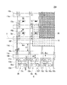
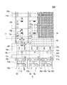
- FIG. 5 is a plan view of the active matrix substrate 200 showing the layout of the protection circuit of the first embodiment. 5 differs from FIG. 3 in that some of the plurality of connection wirings that electrically connect the scanning common wiring 10b and the protection TFT 6b that constitutes the protection diode 6 are in the same layer as the signal line 11a.
- the connection wiring 11e comprised by these is used.
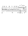
- connection wiring 11e that electrically connects the scanning common wiring 10b and the gate 10g of the protection TFT 6b is formed in the same layer as the signal line 11a.
- some of the connection wirings 11e among the plurality of connection wirings that electrically connect the scanning common wiring 10b and the protection TFT 6b are configured in the same layer as the signal lines 11a.
- the remaining connection wiring 10f among the plurality of connection wirings is configured as a wiring integrated with the scanning common wiring 10b as in the comparative example shown in FIG. For example, although three protection diodes 6 are shown in FIG.
- connection wiring 11e of the protection diode 6 at the left end is composed of a wiring in the same layer as the signal line 11a.
- the connection wiring 10f of the protection diode 6 at the center and the right end is constituted by wiring integrated with the scanning common wiring 10b.
- the protection circuit 30 is formed, the number of the protection TFTs 6b electrically connected to the scanning common wiring 10b independent in one island shape is adjusted, and the scanning line 10a is adjacent to the scanning TFT 10b.
- the breakdown phenomenon due to static electricity between the wirings, in this case, the scanning common wiring 10b can be suppressed.
- Sai [ ⁇ m 2 ] on the left side of (Expression 5) is a value related to the semiconductor layer 13a of the i-th pixel TFT5. Since this value is determined by constraints such as the performance of the pixel TFT 5 and the manufacturing process, it is the same value for all the pixel TFTs 5.
- the value is Sa [ ⁇ m 2 ].
- Sbj [ ⁇ m 2 ] on the right side of (Expression 5) is a value related to the semiconductor layer 13a of the j-th protection TFT 6b. Since this value is determined by constraints such as the performance of the protection TFT 6b and the manufacturing process, it is the same value for all the protection TFTs 6b.
- the value is Sb [ ⁇ m 2 ].
- M [pieces] in (Expression 5) represents the number of pixel TFTs 5 electrically connected to one island-like independent scanning line 10a.
- n [pieces] are protections electrically connected to one island-like independent scanning common line 10b before the formation of the protection circuit, specifically, before the formation of the signal line 11a. This represents the number of TFTs 6b.
- connection wirings among the plurality of connection wirings that electrically connect the scanning common wiring 10b and the protective TFT 6b that are independent in a single island shape are connected.
- the wiring can be adjusted depending on whether the connection wiring 11e in the same layer as the signal line 11a is used. That is, the area of the overlapping portion between the semiconductor layer 13a of the plurality of pixel TFTs 5 and the scanning line 10a, and the semiconductor layer 13a and the scanning common wiring 10b of the protective TFT 6b electrically connected to the scanning common wiring 10b by the connection wiring 10f. And the area of the overlapping portion may be substantially equal.
- n ′ (2400 ⁇ 52.25) /244 ⁇ 513.9 [pieces] It becomes. Therefore, until the protection circuit 30 is formed, the number of protection TFTs 6b electrically connected to one island-like independent scanning common wiring 10b is set to 514 [ [Piece].
- the number of protective TFTs 6b electrically connected to the scanning common wiring 10b independent in a single island shape is optimal as long as it is 514 [pieces], but it is not necessarily limited to 514.
- the value may be about 412 to 616. The reason is as follows.
- the amount of charge Qg at which the gate insulating film 14 of the pixel TFT 5 is destroyed is expressed by (Equation 7) assuming that the gate capacitance Cg of the pixel TFT 5 and the breakdown voltage Vg (> 0) of the gate insulating film 14 of the pixel TFT 5.
- Qg Cg ⁇ Vg [C] (Expression 7) Therefore, the difference ⁇ Qg in the amount of charge that destroys the gate insulating film 14 of the pixel TFT 5 is expressed by (Expression 8).
- a charge 21 of a charge amount qg [C / ⁇ m 2 ] per unit area that destroys the gate insulating film 14 of the pixel TFT 5 is expressed by (Expression 9) from (Expression 3).
- ⁇ qg ⁇ Qg / ⁇ Sai [C / ⁇ m 2 ] (Formula 9)
- the gate insulating film 14 of the pixel TFT 5 cannot be avoided due to the inherent properties of the material.
- the charge quantity Qi at which the interlayer insulating film 15 at the interval D1 between the scanning line 10a and the adjacent wiring, in this case, the scanning common wiring 10b is destroyed is the interlayer capacitance Ci and the breakdown voltage Vi (> 0) of the interlayer insulating film 15. Then, it is expressed by (Equation 10).
- Qi Ci ⁇ Vi [C] (Expression 10) Therefore, the difference ⁇ Qi in the amount of charge that destroys the interlayer insulating film 15 in the interval D1 between the scanning line 10a and the adjacent wiring, in this case, the scanning common wiring 10b is expressed by (Equation 11).
- the interlayer insulating film 15 between the scanning line 10a and its adjacent wiring, in this case, the scanning common wiring 10b, is destroyed before the gate insulating film 14 of the pixel TFT5. Therefore, the effect of the present invention is extremely reduced.
- the number of the protective TFTs 6b may be a value of about 412 to 616, for example.
- n before adjustment is equal to the number of scanning lines 10a and is 1280 [pieces] as seen in FIG.
- the ratio of using the connection wiring 11e to a part of the plurality of connection wirings that electrically connect the scanning common wiring 10b and the protective TFT 6b that are independent in a single island shape is approximately 5 out of 5
- the ratio of 3 is set.
- the reason for setting at such a ratio is to prevent local accumulation of charges caused by electrostatic induction when viewed over the entire surface of the scanning common wiring 10b that is independent in a single island shape. This is to suppress the destruction phenomenon caused by static electricity. It is preferable to set in this way.
- the wiring width A1 of the scanning line 10a independent in one island shape is set to 25 [ ⁇ m]
- the wiring length is set to 94000 [ ⁇ m]
- the scanning common wiring 10b independent in one island shape is set.
- the wiring width B1 is set to 15 [ ⁇ m]
- the wiring length is set to 150,000 [ ⁇ m]. This value is obtained by making the area of one island-like independent scanning line 10a and the area of one island-like independent scanning common line 10b substantially equal to each other so that the amount of charge stored directly in each island is as much as possible. This is the value set to
- the ratio of the area of the scanning common wiring 10b independent to one island to the area of the scanning line 10a independent to one island may be set between +0.8 to +1.2. preferable.
- the wiring width C1 of the auxiliary capacitance line 11d is set to 220 [ ⁇ m]
- the interval D1 between the scanning line 10a and the scanning common wiring 10b is set to 10 [ ⁇ m].
- the protective TFT 6a or the protective TFT 6b generates a discharge, and the electric charges are transferred to the scanning common wiring 10b or the signal It is possible to escape to the common wiring 11b and prevent the phenomenon of destruction due to static electricity.
- FIGS. 3, 4A, and 4B The basic configuration of the liquid crystal display device of the second embodiment is as described with reference to FIGS. 3, 4A, and 4B, but the configuration related to the protection circuit is different from FIGS. 3, 4A, and 4B. 7 and 8, the same reference numerals are given to the same components as those in FIGS. 3, 4A, and 4B used in the description of the basic configuration, and the detailed description thereof is omitted.
- FIG. 7 is a plan view showing a layout of the protective TFTs 6a and 6b of the active matrix substrate 300 of the present embodiment. 7 differs from FIG. 3 in that the connection wiring 11e in the same layer as the signal line 11a is used for all of the plurality of connection wirings that electrically connect the scanning common wiring 10b and the protection TFT 6b.
- a plurality of semiconductor layers 13b (second semiconductor layers) that are the same as the semiconductor layer 13a (first semiconductor layer) for TFT are provided, and a part of the semiconductor layer 13b overlaps the scanning common wiring 10b in a plane.
- a relay wiring 11f of the same layer as the signal line 11a is provided, and a part of the relay wiring 11f overlaps the scanning common wiring 10b in a plan view.
- the first end portion (lower end portion in FIG. 7) of the semiconductor layer 13b overlaps the scanning common wiring 10b in a plan view, and the second end portion (upper end portion in FIG. 7) of the semiconductor layer 13b. However, it protrudes to one side (the upper side in FIG. 7) of the scanning common wiring 10b in the width direction.
- FIG. 8 is a cross-sectional view taken along the line V-VI in FIG.
- the present embodiment (FIGS. 7 and 8) is further different from the basic configuration (FIGS. 3, 4A and 4B) in that the contact hole 16i is formed when the protection circuit 30 is formed, as shown in FIG.
- the scanning common line 10b and the relay line 11f are electrically connected to each other, and the relay line 11f and the semiconductor layer 13b are electrically connected to each other through the contact hole 16h. That is, the scanning common wiring 10b and the semiconductor layer 13b are electrically connected via the relay wiring 11f.
- the area of the semiconductor layer 13b that overlaps the scanning common wiring 10b that is independent in a single island shape is adjusted in plan view, and the scanning line 10a and its scanning line 10a are adjusted. It is possible to prevent a breakdown phenomenon due to static electricity between adjacent wirings, in this case, the scanning line 10a and the scanning common wiring 10b.
- the area of the overlapping portion of the plurality of pixel circuit semiconductor layers 13a and the scanning line 10a is substantially equal to the area of the overlapping portion of the plurality of semiconductor layers 13b and the scanning common wiring 10b. To do.
- Sai [ ⁇ m 2 ] on the left side of (Expression 5) is a value related to the semiconductor layer 13a of the i-th pixel TFT5. Since this value is determined by restrictions on the performance of the pixel TFT 5, the manufacturing process, etc., it is the same value for all the pixel TFTs 5. Let that value be Sa.
- Sbj [ ⁇ m 2 ] on the right side of (Expression 5) represents the area of each of the semiconductor layers 13b overlapping the scanning common wiring 10b independent in a single island shape when seen in a plan view. In the present embodiment, for the sake of convenience, the area of each overlapping portion is set to a predetermined value, and the value is Sb ′.
- M (pieces) in (Expression 5) represents the number of pixel TFTs 5 that are electrically connected to one island-like independent scanning line 10a.
- n [pieces] represents the number of semiconductor layers 13b overlapping with the scanning common wiring 10b independent in a single island shape in a plan view.
- each semiconductor layer 13b overlapping the scanning common wiring 10b independent in a single island shape is optimal if it is 97.97 [ ⁇ m 2 ], but it is not necessarily equal to 97.97 [ ⁇ m 2 ]. You don't have to. For example, the value may be about 79 to 117 [ ⁇ m 2 ]. The reason is as follows.
- the number of the protective TFTs 6b may be a value of about 79 to 117 [ ⁇ m 2 ], for example.
- the wiring width and wiring length of the scanning line 10a independent in one island shape is set to the same value as in the first embodiment. This value is obtained by making the area of one island-like independent scanning line 10a and the area of one island-like independent scanning common line 10b substantially equal to each other so that the amount of charge stored directly in each island is as much as possible. This is the value set to
- the ratio of the area of the scanning common wiring 10b independent to one island to the area of the scanning line 10a independent to one island may be set between +0.8 to +1.2. preferable.
- the length of one side of the area Sb ′ of each semiconductor layer 13b overlapping the scanning common wiring 10b independent in a single island shape (dimension in the direction perpendicular to the direction in which the scanning common wiring 10b extends) E1 is set to 10.1 [ ⁇ m].
- the length of the other side (dimension in the direction parallel to the direction in which the scanning common wiring 10b extends) E2 is set to 9.7 [ ⁇ m].
- the scanning common line 10b and the relay line 11f are electrically connected via the contact hole 16i, and the relay line 11f and the semiconductor layer 13b are electrically connected via the contact hole 16h. Connected. As a result, charges accumulated in the semiconductor layer 13b are released to the scanning common line 10b, and accumulation of charges due to electrostatic induction of the scanning common line 10b is prevented.
- the protection circuit 30 when the scanning line 10a or the signal line 11a becomes a high voltage due to the accumulation of charges, the protection TFT 6a or the protection TFT 6b is discharged, and the charges are discharged to the scanning common wiring 10b or the signal common. By letting it escape to the wiring 11b, it is possible to prevent a breakdown phenomenon due to static electricity.
- connection wiring 11e in the same layer as the signal line 11a is used for all the connection wirings that electrically connect the scanning common wiring 10b and the protection TFT 6b. Thereby, destruction of the protective TFT 6b due to static electricity when charges are accumulated in the scanning common wiring 10b can be avoided.
- FIGS. 3, 4A, and 4B The basic configuration of the liquid crystal display device according to the third embodiment is as described with reference to FIGS. 3, 4A, and 4B, but the configuration related to the protection circuit is different from FIGS. 3, 4A, and 4B. 9 and 10, the same reference numerals are given to the same components as those in FIGS. 3, 4 ⁇ / b> A, and 4 ⁇ / b> B used in the description of the basic configuration, and detailed description thereof is omitted.
- FIG. 9 is a plan view showing a layout of the protective TFTs 6a and 6b of the active matrix substrate 400 of the present embodiment. 9 differs from FIG. 3 in that the connection wiring 11e in the same layer as the signal line 11a is used for all of the plurality of connection wirings that electrically connect the scanning common wiring 10b and the protection TFT 6b.
- a semiconductor capacitor 13c (second semiconductor layer) that is the same layer as the semiconductor layer 13a (first semiconductor layer) for the protective TFT is provided.
- one semiconductor layer 13c is provided for each column of pixels PX arranged in the direction in which the scanning line 10a extends.
- the first end portion (upper end portion in FIG. 9) of the semiconductor layer 13c overlaps the storage capacitor line 10d in a plan view, and the second end portion (lower end portion in FIG. 9) of the semiconductor layer 13c is the storage capacitor line 10d. It protrudes to one side in the width direction (downward in FIG. 9).
- FIG. 10 is a cross-sectional view taken along line VII-VIII in FIG.
- This embodiment (FIGS. 9 and 10) is further different from the basic configuration (FIGS. 3, 4A and 4B) in that the contact hole 16i is formed when the protection circuit 30 is formed, as shown in FIG.
- the auxiliary capacitance line 10d and the relay wiring 11g are electrically connected to each other, and the relay wiring 11g and the semiconductor layer 13c are electrically connected to each other through the contact hole 16h. That is, the auxiliary capacitance line 10d and the semiconductor layer 13c are electrically connected via the relay wiring 11g.
- the area of the semiconductor layer 13c overlapping the auxiliary capacitance line 10d that is independent in a single island shape is adjusted in plan view, and the scanning line 10a is adjacent to the area. Wiring, in this case, a breakdown phenomenon due to static electricity between the scanning line 10a and the auxiliary capacitance line 10d can be prevented.
- the area of the overlapping portion of the plurality of pixel circuit semiconductor layers 13a and the scanning line 10a is substantially equal to the area of the overlapping portion of the plurality of semiconductor layers 13c and the auxiliary capacitance line 10d. To do.
- Sai [ ⁇ m 2 ] on the left side of (Expression 5) is a value related to the semiconductor layer 13a of the i-th pixel TFT5. Since this value is determined by restrictions on the performance of the pixel TFT 5, the manufacturing process, etc., it is the same value for all the pixel TFTs 5. Let that value be Sa.
- Sbj [ ⁇ m 2 ] on the right side of (Expression 5) represents the area of each semiconductor layer 13c that overlaps the single auxiliary capacitance line 10d in an island shape when seen in a plan view. In the present embodiment, for the sake of convenience, each area is set to a predetermined value, and the value is Sb ′.
- M (pieces) in (Expression 5) represents the number of pixel TFTs 5 electrically connected to one island-like independent scanning line 10a.
- n [pieces] represents the number of semiconductor layers 13c overlapping with the auxiliary capacitance line 10d independent in a single island shape when seen in a plan view.
- the value of Sb ′ when the value of Sb ′ is obtained from (Equation 5), it is 97.97 [ ⁇ m 2 ] as in the second embodiment. Note that, similarly to the second embodiment, the value of Sb ′ may be a value of about 79 to 117 [ ⁇ m 2 ], for example.
- the wiring width of the scanning line 10a independent in one island shape, the wiring width and wiring length of the scanning common wiring 10b independent in one island shape, and the wiring width of the auxiliary capacitance line 10d are the same as those in the first embodiment. It is the same value.
- the wiring length of the scanning line 10a is set to 93700 [ ⁇ m].
- a distance D2 between the scanning line 10a and the auxiliary capacitance line 10d is set to 10 [ ⁇ m].
- the length of one side of the area Sb ′ of each of the semiconductor layers 13c that overlaps the single auxiliary capacitor line 10d in the shape of an island (dimension in the direction perpendicular to the direction in which the auxiliary capacitor line 10d extends).
- F1 is set to 10.1 [ ⁇ m].
- F2 is set to 9.7 [ ⁇ m].
- the auxiliary capacitance line 10d and the relay wiring 11g are electrically connected via the contact hole 16i, and the relay wiring 11g and the semiconductor layer 13c are electrically connected via the contact hole 16h. Connected. Thereby, the charge accumulated in the semiconductor layer 13c can be released to the auxiliary capacitance line 10d, and the accumulation of the charge due to the electrostatic induction of the auxiliary capacitance line 10d can be eliminated.
- the auxiliary capacitance line 10d and the relay wiring 11g are stacked, the resistance value of the entire wiring is reduced. Therefore, a voltage can be stably applied to the common electrode 18 when the liquid crystal display device 50 is driven.
- the protection circuit 30 when the scanning line 10a or the signal line 11a becomes a high voltage due to the accumulation of charges, the protection TFT 6a or the protection TFT 6b is discharged, and the charges are discharged to the scanning common wiring 10b or the signal common. By letting it escape to the wiring 11b, the phenomenon of destruction due to static electricity can be suppressed.
- connection wiring 11e in the same layer as the signal line 11a is used for all the connection wirings that electrically connect the scanning common wiring 10b and the protection TFT 6b. Thereby, destruction of the protective TFT 6b due to static electricity when charges are accumulated in the scanning common wiring 10b can be avoided.
- FIGS. 11 and 12 a liquid crystal display device according to a fourth embodiment will be described with reference to FIGS. 11 and 12.
- the basic configuration of the liquid crystal display device of the fourth embodiment is as described with reference to FIGS. 3, 4A, and 4B, but the configuration related to the protection circuit is different from FIGS. 3, 4A, and 4B. 11 and 12, the same reference numerals are given to the same components as those in FIGS. 3, 4A, and 4B used in the description of the basic configuration, and the detailed description thereof is omitted.
- FIG. 11 is a plan view showing a layout of the protective TFTs 6a and 6b of the active matrix substrate 500 of the present embodiment. 11 differs from FIG. 3 in that the connection wiring 11e in the same layer as the signal line 11a is used for all of the plurality of connection wirings that electrically connect the scanning common wiring 10b and the protection TFT 6b.
- a plurality of semiconductor layers 13b (second semiconductor layers) that are the same as the semiconductor layer 13a (first semiconductor layer) for TFT are provided, and a part of the semiconductor layer 13b overlaps the scanning common wiring 10b in a plane.
- a relay wiring 11f of the same layer as the signal line 11a is provided, and a part of the relay wiring 11f overlaps the scanning common wiring 10b in a plan view.
- one end portion (upper end portion in FIG. 7) of the semiconductor layer 13b protrudes to one side (upward in FIG. 7) in the width direction of the scanning common wiring 10b.
- the central portion of the semiconductor layer 13b overlaps the scanning common wiring 10b in a plan view, and both end portions (the upper end portion and the lower end portion in FIG. 11) of the semiconductor layer 13b are the scanning common wiring 10b. It protrudes on both sides in the width direction.
- FIG. 12 is a cross-sectional view taken along line IX-X in FIG.
- This embodiment (FIGS. 11 and 12) is further different from the basic configuration (FIGS. 3, 4A and 4B) in that the contact hole 16i is formed at the time when the protection circuit 30 is formed, as shown in FIG.
- the scanning common wiring 10b and the relay wiring 11f are electrically connected to each other, and the relay wiring 11f and the semiconductor layer 13b are electrically connected to each other through two contact holes 16h provided with the scanning common wiring 10b interposed therebetween. It is a point connected to. That is, the scanning common wiring 10b and the semiconductor layer 13b are electrically connected via the relay wiring 11f.
- the area of the semiconductor layer 13b that overlaps the scanning common wiring 10b independent in a single island shape is adjusted in plan view, and the scanning line 10a is adjacent to the scanning line 10a. Wiring, in this case, a breakdown phenomenon due to static electricity between the scanning line 10a and the scanning common wiring 10b can be suppressed.
- the area of the overlapping portion of the plurality of pixel TFT semiconductor layers 13a and the scanning line 10a is substantially equal to the area of the overlapping portion of the plurality of semiconductor layers 13b and the scanning common wiring 10b. To do.
- Sai [ ⁇ m 2 ] on the left side of (Expression 5) is a value related to the semiconductor layer 13a of the i-th pixel TFT5. Since this value is determined by restrictions on the performance of the pixel TFT 5, the manufacturing process, etc., it is the same value for all the pixel TFTs 5. Let that value be Sa.
- Sbj [ ⁇ m 2 ] on the right side of (Expression 5) represents the area of each of the semiconductor layers 13b overlapping the scanning common wiring 10b independent in a single island shape when seen in a plan view. In the present embodiment, for the sake of convenience, the area of each overlapping portion is set to a predetermined value, and the value is Sb ′.
- M (pieces) in (Expression 5) represents the number of pixel TFTs 5 electrically connected to one island-like independent scanning line 10a.
- n [pieces] represents the number of semiconductor layers 13b overlapping with the scanning common wiring 10b independent in a single island shape in a plan view.
- the wiring width and wiring length of the scanning line 10a independent in one island shape is set to the same value as in the first embodiment. This value is set so that the area of one island-like independent scanning line 10a and the area of one island-like independent scanning common line 10b are approximately equal, and the amount of charge stored directly in each is as much as possible. It is a value set to make it equal.
- the ratio of the area of the scanning common wiring 10b independent to one island to the area of the scanning line 10a independent to one island may be set between +0.8 to +1.2. preferable.
- the length of one side of the area Sb ′ of each semiconductor layer 13b overlapping the scanning common wiring 10b independent in a single island shape (dimension in the direction perpendicular to the direction in which the scanning common wiring 10b extends) G1 is set to 15 [ ⁇ m].
- the length of the other side (dimension in the direction parallel to the direction in which the scanning common wiring 10b extends) G2 is set to 6.5 [ ⁇ m].
- the area Sb ′ becomes 97.5 [ ⁇ m 2 ], which can be close to the value at which ⁇ Q is the minimum, that is, 97.97 [ ⁇ m 2 ], which is the value calculated in the second embodiment.
- a slight misalignment may be unavoidable between the patterns of each layer.
- a misalignment between the scanning common line 10b and the semiconductor layer 13b occurs.
- the scanning common wiring 10b and the semiconductor layer 13b are displaced in a direction parallel to the extending direction of the scanning common wiring 10b, the area of the overlapping portion between the scanning common wiring 10b and the semiconductor layer 13b changes. Absent.
- the scanning common wiring 10b and the semiconductor layer 13b are shifted in the direction perpendicular to the extending direction of the scanning common wiring 10b (the vertical direction in the figure), the scanning common wiring 10b.
- the area of the overlapping portion between the semiconductor layer 13b and the semiconductor layer 13b changes, and the effect of suppressing the breakdown phenomenon due to static electricity is reduced.
- both end portions (upper end portion and lower end portion in FIG. 11) of the semiconductor layer 13b protrude from both sides of the scanning common wiring 10b in the width direction. Therefore, even if the scanning common wiring 10b and the semiconductor layer 13b are displaced in the direction perpendicular to the direction in which the scanning common wiring 10b extends (the vertical direction in FIG. 11), the overlapping portion of the scanning common wiring 10b and the semiconductor layer 13b The area does not change. Therefore, even when an alignment shift caused by a manufacturing process or the like occurs, it is possible to maintain the effect of suppressing the phenomenon of breakdown due to static electricity.
- the scanning common line 10b and the relay line 11f are electrically connected via the contact hole 16i, and the relay line 11f and the semiconductor layer 13b are electrically connected via the contact hole 16h. Connected.
- the charges accumulated in the semiconductor layer 13b can be released to the scanning common line 10b, and the accumulation of charges due to electrostatic induction of the scanning common line 10b can be eliminated.
- the protection TFT 6a or the protection TFT 6b discharges and charges are transferred to the scanning common wiring 10b or signal common. By letting it escape to the wiring 11b, it is possible to prevent a breakdown phenomenon due to static electricity.
- connection wiring 11e in the same layer as the signal line 11a is used for all the connection wirings that electrically connect the scanning common wiring 10b and the protection TFT 6b. Thereby, destruction of the protective TFT 6b due to static electricity when charges are accumulated in the scanning common wiring 10b can be avoided.
- FIGS. 13 and 14 The basic configuration of the liquid crystal display device according to the fifth embodiment is as described with reference to FIGS. 3, 4A, and 4B, but the configuration related to the protection circuit is different from FIGS. 3, 4A, and 4B. 13 and 14, the same reference numerals are given to the same components as those in FIGS. 3, 4 ⁇ / b> A, and 4 ⁇ / b> B used in the description of the basic configuration, and detailed description thereof is omitted.
- FIG. 13 is a plan view showing the layout of the protective TFTs 6a and 6b of the active matrix substrate 600 of this embodiment. 13 differs from FIG. 3 in that the connection wiring 11e in the same layer as the signal line 11a is used for all of the plurality of connection wirings that electrically connect the scanning common wiring 10b and the protection TFT 6b.
- a semiconductor capacitor 13c (second semiconductor layer) that is the same layer as the semiconductor layer 13a (first semiconductor layer) for the protective TFT is provided.
- one semiconductor layer 13c is provided for each pixel column, and one end portion (lower end portion in FIG. 9) of the semiconductor layer 13c is on one side in the width direction of the auxiliary capacitance line 10d (FIG. 9). It protruded to the bottom).
- two semiconductor layers 13c are provided for each column of pixels PX arranged in the extending direction of the scanning line 10a, and the two semiconductor layers 13c are provided on the upper side of the auxiliary capacitance line 10d. It is arranged on the side and the lower side.
- the first ends of the two semiconductor layers 13c overlap the storage capacitor line 10d in a plan view.
- the second ends of the two semiconductor layers 13c (the ends of the two semiconductor layers 13c in FIG. 13 that are separated from each other) are on both sides in the width direction of the storage capacitor line 10d (the vertical direction in FIG. 13). It is sticking out.
- FIG. 14 is a sectional view taken along line XI-XII in FIG.
- the present embodiment (FIGS. 13 and 14) is further different from the basic configuration (FIGS. 3, 4A and 4B) in that the auxiliary capacitance line 10d is formed via the contact hole 16i when the protection circuit 30 is formed.
- the relay wiring 11g are electrically connected (see FIG. 13), and the relay wiring 11g and the semiconductor layer 13c are electrically connected via the contact hole 16h (see FIGS. 13 and 14). . That is, the auxiliary capacitance line 10d and the semiconductor layer 13c are electrically connected via the relay wiring 11g.
- the area of the semiconductor layer 13c overlapping the auxiliary capacitance line 10d that is independent in a single island shape is adjusted in plan view, and the scanning line 10a is adjacent to the area. Wiring, in this case, a breakdown phenomenon due to static electricity between the scanning line 10a and the auxiliary capacitance line 10d can be suppressed.
- the area of the overlapping portion of the plurality of pixel circuit semiconductor layers 13a and the scanning line 10a is substantially equal to the area of the overlapping portion of the plurality of semiconductor layers 13c and the auxiliary capacitance line 10d. To do.
- Sai [ ⁇ m 2 ] on the left side of (Expression 5) is a value related to the semiconductor layer 13a of the i-th pixel TFT5. Since this value is determined by restrictions on the performance of the pixel TFT 5, the manufacturing process, etc., it is the same value for all the pixel TFTs 5. Let that value be Sa.
- Sbj [ ⁇ m 2 ] on the right side of (Formula 5) represents the area of each semiconductor layer 13c overlapping with the auxiliary capacitance line 10d that is independent in a single island shape when seen in a plan view. In the present embodiment, for the sake of convenience, each area is set to a predetermined value, and the value is Sb ′.
- M (pieces) in (Expression 5) represents the number of pixel TFTs 5 that are electrically connected to one island-like independent scanning line 10a.
- n [pieces] represents the number of semiconductor layers 13c overlapping with the auxiliary capacitance line 10d independent in a single island shape when seen in a plan view.
- each of the semiconductor layers 13b overlapping the single auxiliary capacitor line 10d in an island shape is optimal if it is 48.98 [ ⁇ m 2 ], but does not necessarily match 48.98 [ ⁇ m 2 ]. It does not have to be. For example, the value may be about 40 to 58 [ ⁇ m 2 ]. The reason is as follows.
- the area of each of the semiconductor layers 13b overlapping the single auxiliary capacitance line 10d in the shape of an island may have a value of about 40 to 58 [ ⁇ m 2 ], for example.
- the wiring width of the scanning line 10a independent in one island shape, the wiring width and wiring length of the scanning common wiring 10b independent in one island shape, and the wiring width of the auxiliary capacitance line 10d are the same as those in the first embodiment. It is the same value.
- the wiring length of the scanning line 10a and the interval between the scanning line 10a and the auxiliary capacitance line 10d are the same values as in the third embodiment.
- H1 is set to 7.9 [ ⁇ m].
- the length of the other side (dimension in the direction parallel to the direction in which the auxiliary capacitance line 10d extends) H2 is set to 6.2 [ ⁇ m].
- two semiconductor layers 13c are provided for each pixel column, and the end portions of the two semiconductor layers 13c that are separated from each other protrude from both sides of the auxiliary capacitance line 10d in the width direction. . Therefore, even if the auxiliary capacitance line 10d and the semiconductor layer 13c are displaced in the direction perpendicular to the direction in which the auxiliary capacitance line 10d extends (the vertical direction in FIG. 13), the overlapping portion of the auxiliary capacitance line 10d and the semiconductor layer 13c. The area does not change. Therefore, even when an alignment shift caused by a manufacturing process or the like occurs, it is possible to maintain the effect of suppressing the phenomenon of breakdown due to static electricity.
- the auxiliary capacitance line 10d and the relay wiring 11g are electrically connected via the contact hole 16i, and the relay wiring 11g and the semiconductor layer 13c are electrically connected via the contact hole 16h. Connected. Thereby, the charge accumulated in the semiconductor layer 13c can be released to the auxiliary capacitance line 10d, and the accumulation of the charge due to the electrostatic induction of the auxiliary capacitance line 10d can be eliminated.
- the entire wiring has a laminated structure of the auxiliary capacitance line 10d and the relay wiring 11g, the resistance value of the wiring is reduced, and a voltage can be stably applied to the common electrode 18 when the liquid crystal display device is driven. it can.
- the protection circuit 30 after the protection circuit 30 is formed, when the scanning line 10a or the signal line 11a becomes a high voltage due to the accumulation of electric charge, the protection TFT 6a or the protection TFT 6b discharges and charges are transferred to the scanning common wiring 10b or signal common. By letting it escape to the wiring 11b, it is possible to prevent a breakdown phenomenon due to static electricity.
- connection wiring 11e in the same layer as the signal line 11a is used for all the connection wirings that electrically connect the scanning common wiring 10b and the protection TFT 6b. Thereby, destruction of the protective TFT 6b due to static electricity when charges are accumulated in the scanning common wiring 10b can be avoided.
- each TFT constituting the pixel TFT and the protective TFT can be changed to a group 14 element semiconductor such as silicon, an oxide semiconductor, or the like.
- the crystallinity of the semiconductor material of each TFT is not particularly limited, and may be single crystal, polycrystal, amorphous, or microcrystal.
- the oxide semiconductor contains at least one element selected from the group consisting of indium (In), gallium (Ga), zinc (Zn), aluminum (Al), and silicon (Si), and oxygen (O). It is preferable that In, Ga, Zn, and O are included.
- the form of each TFT constituting the pixel TFT and the protection TFT is not particularly limited to the top gate method, and can be appropriately changed to, for example, a bottom gate method.
- FIG. 15 is a schematic diagram illustrating an example of a pixel circuit of an organic EL display device.
- the pixel includes a first transistor T1, a second transistor T2, a capacitor Cst, and an organic light emitting diode (OLED).
- the first transistor T1 has a source connected to the first power supply ELVDD, a drain connected to the anode electrode of the organic light emitting diode, and a gate connected to the first node N1.
- the second transistor T2 has a source connected to the data line Dm, a drain connected to the first node N1, and a gate connected to the scanning line Sn.
- the capacitor Cst has a first electrode connected to the first power supply ELVDD and a second electrode connected to the first node N1.
- the organic light emitting diode has an anode electrode connected to the drain of the first transistor T1, and a cathode electrode connected to the second power source ELVSS.
- the present invention can also be applied to organic EL display devices because of the presence of scanning lines.
- the present invention is not limited to a liquid crystal display device and can be applied to various display devices.
- the present invention can be used for various display devices such as liquid crystal display devices and organic EL display devices.
- Pixel TFT pixel circuit TFT
- Protection diode protection element
- 10a ... Scanning line
- 10b Scanning common wiring (common wiring)
- 11a Signal line
- 10d, 11d ...
- 10f, 11e Connection wiring
- 11f, 11g Relay wiring
- 13a, 13b, 13c Semiconductor layer
- 50 Liquid crystal display device
- PX Pixel.
Landscapes
- Physics & Mathematics (AREA)
- Nonlinear Science (AREA)
- Engineering & Computer Science (AREA)
- Microelectronics & Electronic Packaging (AREA)
- Mathematical Physics (AREA)
- Crystallography & Structural Chemistry (AREA)
- Chemical & Material Sciences (AREA)
- General Physics & Mathematics (AREA)
- Optics & Photonics (AREA)
- Liquid Crystal (AREA)
- Thin Film Transistor (AREA)
- Devices For Indicating Variable Information By Combining Individual Elements (AREA)
- Electroluminescent Light Sources (AREA)
- Power Engineering (AREA)
Abstract
Description
本願は、2014年4月8日に、日本に出願された特願2014-079514号に基づき優先権を主張し、その内容をここに援用する。
以下、本発明の第1実施形態について、図1~図6を用いて説明する。
本実施形態では、表示装置として、アクティブマトリクス基板を備えた液晶表示装置の一例を挙げる。
なお、以下の各図面においては各構成要素を見やすくするため、構成要素によって寸法の縮尺を異ならせて示すことがある。
図1は、アクティブマトリクス型の液晶表示装置の斜視図である。
図1に示すように、液晶表示装置50は、例えば、互いに対向するように設けられたアクティブマトリクス基板100および対向基板150と、アクティブマトリクス基板100と対向基板150との間に挟持された液晶層(図示せず)と、を備えている。液晶表示装置50には、画像表示を行う表示領域1と、表示領域1の周囲を囲む額縁領域2と、がそれぞれ設けられている。
図2に示すように、アクティブマトリクス基板100は、例えば、矩形状の表示領域1において、互いに平行に延びるように設けられた複数の走査線10aと、各走査線10aと直交する方向に互いに平行に延びるように設けられた複数の信号線11aとを備えている。
そこで、TFTや配線が破壊されることを防止するため、アクティブマトリクス基板100は、以下に説明する保護回路30を備えている。
本実施形態の「保護ダイオード6」は、特許請求の範囲の「保護素子」に相当する。
図4Aは、図3のI-IIに沿う断面図である。
図3および図4Aにおいては、半導体層13aの上層側(図4Aの上方向)に走査線10aを配置する方式のTFTであるトップゲートTFTを図示している。
以下、図3と図4Aとを参照して、アクティブマトリクス基板100の製造方法について記述する。
まず、ガラス基板などの透明基板40上に、例えば、CVD(Chemical Vapor Deposition)法により、窒化シリコン膜、酸化シリコン膜またはそれらの積層膜などを厚さ50nm程度で成膜して、下地膜12を形成する。
続いて、下地膜12が形成された基板全体に、例えば、CVD法により、真性アモルファスシリコン膜を厚さ50nm程度で成膜する。その後、レーザー光照射などのアニール処理により真性アモルファスシリコン膜を多結晶化し、ポリシリコン膜を形成する。そのポリシリコン膜に対して、フォトリソグラフィ処理、エッチング処理およびレジストの剥離処理を行うことにより、半導体層13aなどを形成する。
さらに、ゲート絶縁膜14が形成された基板全体に、例えば、スパッタリング法により、タングステン膜などの金属膜を厚さ300nm程度で成膜する。その後、その金属膜に対して、フォトリソグラフィ処理、エッチング処理およびレジスト剥離処理を行うことにより、走査線10a、走査共通配線10b、および、その他のゲート配線10cなどを形成する。
さらに、半導体層13aのチャネル領域、ソース領域およびドレイン領域が形成された基板全体に、例えば、CVD法により、窒化シリコン膜、酸化シリコン膜またはそれらの積層膜などの無機絶縁膜を厚さ700[nm]程度で成膜する。その後、その無機絶縁膜およびその下層のゲート絶縁膜14に対して、フォトリソグラフィ処理、エッチング処理およびレジスト剥離処理を行うことにより、コンタクトホール16a,16b,16c,16d,16eなどを有する層間絶縁膜15を形成する。
以上の工程により、アクティブマトリクス基板100を製造することができる。
まず、ガラス基板などの透明基板の基板全体に、例えば、スピンコート法またはスリットコート法により、黒色に着色された感光性樹脂を塗布する。その後、その塗布膜を露光および現像することにより、ブラックマトリクスを厚さ1μm程度に形成する。
以上の工程により、対向基板150を製造することができる。
例えば、上記の対向基板製造工程で製造された対向基板150の表面に、UV(紫外線)硬化および熱硬化の併用型樹脂などからなるシール材を枠状に印刷する。その後、シール材の内側に液晶材料を滴下する。
続いて、液晶材料が滴下された対向基板150と、上記のアクティブマトリクス基板製造工程で製造されたアクティブマトリクス基板100とを、減圧雰囲気下で貼り合わせ、その後、大気圧に開放する。
さらに、貼り合わせた状態にて、シール材にUV光を照射した後、加熱することによりシール材を硬化させる。
以上の工程により、図1に示すアクティブマトリクス型の液晶表示装置50を製造することができる。
上述したように、例えばアクティブマトリクス基板100の製造工程におけるフォトリソグラフィ処理などにおいて、ガラス基板と他の部材との接触、摩擦、剥離などが頻繁に発生する。そのため、半導体層13a、走査線10a、および信号線11aなどへの電荷の蓄積は避けられない。この場合、前述したように、静電気によるTFTや配線の破壊を引き起こす場合がある。
q×Sai[c](i=1,2,…,m) …(式1)
q×Sbj[c](j=1,2,…,n) …(式2)
Qa≒Σ(q×Sai)=q×ΣSai[c](i=1,2,…,m) …(式3)
Qb≒Σ(q×Sbj)=q×ΣSbj[c](j=1,2,…,n) …(式4)
ΔQ≒|Qa-Qb|=q×|ΣSai-ΣSbj|
となる。このとき、ΔQが過大になった場合、静電気による破壊現象が発生すると考えられる。
ΣSai=ΣSbj(i=1,2,…,m)(j=1,2,…,n) …(式5)となる。
[第1実施形態]
以下、第1実施形態の液晶表示装置について、図5、図6を用いて説明する。
第1実施形態の液晶表示装置の基本構成は図3、図4A及び図4Bを用いて説明した通りであるが、保護回路に係わる構成が図3、図4A及び図4Bと異なる。
図5、図6において、基本構成の説明で用いた図3、図4A及び図4Bと共通の構成要素には同一の符号を付して、その詳細な説明を省略する。
図5が図3と異なる点は、走査共通配線10bと保護ダイオード6を構成する保護TFT6bとを電気的に接続する複数の接続配線のうちの一部の接続配線に、信号線11aと同層で構成される接続配線11eを使用する点である。
図6に示すように、走査共通配線10bと保護TFT6bのゲート10gとを電気的に接続する接続配線11eは、信号線11aと同層で構成されている。このように、走査共通配線10bと保護TFT6bとを電気的に接続する複数の接続配線のうちの一部の接続配線11eは、信号線11aと同層の配線で構成されている。また、複数の接続配線のうちの残りの接続配線10fは、図3に示した比較例と同様、走査共通配線10bと一体の配線で構成されている。例えば、図5には3個の保護ダイオード6が示されているが、左端の保護ダイオード6の接続配線11eは、信号線11aと同層の配線で構成されている。中央および右端の保護ダイオード6の接続配線10fは、走査共通配線10bと一体の配線で構成されている。
その値をSa[μm2]とする。(式5)の右辺のSbj[μm2]は、j個目の保護TFT6bの半導体層13aに関する値である。この値は、保護TFT6bの性能、製造プロセスなどの制約で決まるため、全ての保護TFT6bに対して同一の値である。その値をSb[μm2]とする。(式5)のm[個]は、1本の島状に独立した走査線10aに対して、電気的に接続された画素TFT5の個数を表す。n[個]は、1本の島状に独立した走査共通配線10bに対して、保護回路形成前の時点、具体的には、信号線11aの形成前の時点で電気的に接続された保護TFT6bの個数を表す。
ΣSai=ΣSbj(i=1,2,…,m)(j=1,2,…,n’)
→ m×Sa=n’×Sb
→ n’=(m×Sa)/Sb[個] …(式6)
となる。
(式6)より、
n’=(2400×52.25)/244≒513.9[個]
となる。
したがって、保護回路30が形成されるまで、1本の島状に独立した走査共通配線10bに対して、電気的に接続された保護TFT6bの個数を、ΔQが最小値になる値として、514[個]にすればよい。
その理由は、以下の通りである。
Qg=Cg×Vg[C] …(式7)
よって、画素TFT5のゲート絶縁膜14が破壊される電荷量の差ΔQgは、(式8)で表わされる。
ΔQg=2×Qg=2×Cg×Vg[C] …(式8)
ΔQg≒Σ(qg×Sai)=qg×ΣSai[C](i=1,2,…,m)
→ qg=ΔQg/ΣSai [C/μm2] …(式9)
Qi=Ci×Vi[C] …(式10)
よって、走査線10aとその隣接する配線、この場合、走査共通配線10bの間隔D1の層間絶縁膜15が破壊される電荷量の差ΔQiは、(式11)で表わされる。
ΔQi=2×Qi=2×Ci×Vi[C] …(式11)
ΔQi=qg×|ΣSai-ΣSbj|
→ |ΣSai-ΣSbj|=ΔQi/qg=(ΔQi×ΣSai)/ΔQg
…(式12)
ΔQg=2×Cg×Vg=4.00×10⁻¹²[C]
であり、(式9)より、
qg=ΔQg/ΣSai≒3.20×10-17[C/μm2]
となる。
ΔQi=2×Ci×Vi=8.00×10⁻¹³[C]
であり、(式12)より、
|ΣSai-ΣSbj|=(ΔQi×ΣSai)/ΔQg≒2.50×104[μm2]となる。
|ΣSai-ΣSbj|=|m×Sa-n’×Sb|<2.50×10⁴ …(式13)であればよいから、m=2400[個]、Sa=52.25[μm2]、Sb=244[μm2]より、
411.5 < n’< 616.4
となる。
なお、補助容量線11dの配線幅C1は220[μm]に設定し、走査線10aと走査共通配線10bの間隔D1は10[μm]に設定する。
以下、第2実施形態の液晶表示装置について、図7、図8を用いて説明する。
第2実施形態の液晶表示装置の基本構成は図3、図4A及び図4Bを用いて説明した通りであるが、保護回路に係わる構成が図3、図4A及び図4Bと異なる。
図7、図8において、基本構成の説明で用いた図3、図4A及び図4Bと共通の構成要素には同一の符号を付して、その詳細な説明を省略する。
図7が図3と異なる点は、走査共通配線10bと保護TFT6bとを電気的に接続する複数の接続配線の全てに、信号線11aと同層の接続配線11eを使用している点、保護TFT用の半導体層13a(第1半導体層)と同層の複数の半導体層13b(第2半導体層)が設けられ、半導体層13bの一部が走査共通配線10bと平面的に重なっている点、および、信号線11aと同層の中継配線11fが設けられ、中継配線11fの一部が走査共通配線10bと平面的に重なっている点、である。
本実施形態(図7、図8)がさらに基本構成(図3、図4A及び図4B)と異なる点は、保護回路30が形成される時点で、図8に示すように、コンタクトホール16iを介して、走査共通配線10bと中継配線11fとが電気的に接続され、コンタクトホール16hを介して、中継配線11fと半導体層13bとが電気的に接続される点である。すなわち、走査共通配線10bと半導体層13bとは、中継配線11fを介して電気的に接続される。
ΣSai=ΣSbj(i=1,2,…,m)(j=1,2,…,n)
→ m×Sa=n×Sb’
→ Sb’=(m×Sa)/n[μm2] …(式14)
となる。
(式14)により、
Sb’=(2400×52.25)/1280≒97.969[μm2]
となる。つまり、平面的に見て、1本の島状に独立した走査共通配線10bと重なる半導体層13bの各々の面積を、ΔQが最小値になる値として、97.97[μm2]にすればよい。
その理由は、以下の通りである。
|ΣSai-ΣSbj|=|m×Sa-n×Sb’|<2.50×10⁴
であればよいから、m=2400[個]、Sa=52.25[μm2]、n=1280[個]より、
78.4 < Sb’< 117.5
となる。
平面的に見て、1本の島状に独立した走査共通配線10bと重なる半導体層13bの各々の面積Sb’の1辺の長さ(走査共通配線10bが延びる方向と垂直な方向の寸法)E1は、10.1[μm]に設定する。他の1辺の長さ(走査共通配線10bが延びる方向と平行な方向の寸法)E2は、9.7[μm]に設定する。
以下、第3実施形態の液晶表示装置について、図9、図10を用いて説明する。
第3実施形態の液晶表示装置の基本構成は図3、図4A及び図4Bを用いて説明した通りであるが、保護回路に係わる構成が図3、図4A及び図4Bと異なる。
図9、図10において、基本構成の説明で用いた図3、図4A及び図4Bと共通の構成要素には同一の符号を付して、その詳細な説明を省略する。
図9が図3と異なる点は、走査共通配線10bと保護TFT6bとを電気的に接続する複数の接続配線の全てに、信号線11aと同層の接続配線11eを用いている点、走査線10aと同層の補助容量線10dを用いている点、保護TFT用の半導体層13a(第1半導体層)と同層の複数の半導体層13c(第2半導体層)が設けられ、半導体層13cの一部が補助容量線10dと平面的に重なっている点、および、信号線11aと同層の中継配線11gが設けられ、中継配線11gの一部が補助容量線10dと平面的に重なっている点、である。
本実施形態(図9、図10)がさらに基本構成(図3、図4A及び図4B)と異なる点は、保護回路30が形成される時点で、図10に示すように、コンタクトホール16iを介して、補助容量線10dと中継配線11gとが電気的に接続され、コンタクトホール16hを介して、中継配線11gと半導体層13cとが電気的に接続される点である。すなわち、補助容量線10dと半導体層13cとは、中継配線11gを介して電気的に接続される。
なお、第2実施形態と同様、Sb’の値は例えば79~117[μm2]程度の値であってもよい。
以下、第4実施形態の液晶表示装置について、図11、図12を用いて説明する。
第4実施形態の液晶表示装置の基本構成は図3、図4A及び図4Bを用いて説明した通りであるが、保護回路に係わる構成が図3、図4A及び図4Bと異なる。
図11、図12において、基本構成の説明で用いた図3、図4A及び図4Bと共通の構成要素には同一の符号を付して、その詳細な説明を省略する。
図11が図3と異なる点は、走査共通配線10bと保護TFT6bとを電気的に接続する複数の接続配線の全てに、信号線11aと同層の接続配線11eを使用している点、保護TFT用の半導体層13a(第1半導体層)と同層の複数の半導体層13b(第2半導体層)が設けられ、半導体層13bの一部が走査共通配線10bと平面的に重なっている点、および、信号線11aと同層の中継配線11fが設けられ、中継配線11fの一部が走査共通配線10bと平面的に重なっている点、である。
本実施形態(図11、図12)がさらに基本構成(図3、図4A及び図4B)と異なる点は、保護回路30が形成される時点で、図12に示すように、コンタクトホール16iを介して、走査共通配線10bと中継配線11fとが電気的に接続され、走査共通配線10bを挟んで設けられた2個のコンタクトホール16hを介して、中継配線11fと半導体層13bとが電気的に接続される点である。すなわち、走査共通配線10bと半導体層13bとは、中継配線11fを介して電気的に接続される。
なお、第2実施形態と同様、Sb’の値は例えば79~117[μm2]程度の値であってもよい。
平面的に見て、1本の島状に独立した走査共通配線10bと重なる半導体層13bの各々の面積Sb’の1辺の長さ(走査共通配線10bが延びる方向と垂直な方向の寸法)G1は、15[μm]に設定する。他の1辺の長さ(走査共通配線10bが延びる方向と平行な方向の寸法)G2は、6.5[μm]に設定する。これにより、面積Sb’は97.5[μm2]となり、ΔQが最小値となる値、つまり、第2実施形態で計算した値である97.97[μm2]に近付けることができる。
以下、第5実施形態の液晶表示装置について、図13、図14を用いて説明する。
第5実施形態の液晶表示装置の基本構成は図3、図4A及び図4Bを用いて説明した通りであるが、保護回路に係わる構成が図3、図4A及び図4Bと異なる。
図13、図14において、基本構成の説明で用いた図3、図4A及び図4Bと共通の構成要素には同一の符号を付して、その詳細な説明を省略する。
図13が図3と異なる点は、走査共通配線10bと保護TFT6bとを電気的に接続する複数の接続配線の全てに、信号線11aと同層の接続配線11eを用いている点、走査線10aと同層の補助容量線10dを用いている点、保護TFT用の半導体層13a(第1半導体層)と同層の複数の半導体層13c(第2半導体層)が設けられ、半導体層13cの一部が補助容量線10dと平面的に重なっている点、および、信号線11aと同層の中継配線11gが設けられ、中継配線11gの一部が補助容量線10dと平面的に重なっている点、である。
本実施形態(図13、図14)がさらに基本構成(図3、図4A及び図4B)と異なる点は、保護回路30が形成される時点で、コンタクトホール16iを介して、補助容量線10dと中継配線11gとが電気的に接続され(図13参照)、コンタクトホール16hを介して、中継配線11gと半導体層13cとが電気的に接続される(図13および図14参照)点である。すなわち、補助容量線10dと半導体層13cとは、中継配線11gを介して電気的に接続される。
ΣSai=ΣSbj(i=1,2,…,m)(j=1,2,…,n)
→ m×Sa=n×Sb’
→ Sb’=(m×Sa)/n[μm2] …(式14)
となる。
このとき、(式14)により、
Sb’=(2400×52.25)/2560≒48.984[μm2]
となる。
よって、平面的に見て、1本の島状に独立した補助容量線10dと重なる半導体層13bの各々の面積を、ΔQが最小値になる値として、48.98[μm2]になるように設計すればよい。
その理由は、以下の通りである。
|ΣSai-ΣSbj|=|m×Sa-n×Sb’|<2.50×10⁴
であればよいから、m=2400[個]、Sa=52.25[μm2]、n=2×1280=2560[個]より、
39.2 < Sb’< 58.8
となる。
例えば、画素TFTと保護TFTを構成する各TFTの半導体材料は、シリコン等の14族元素の半導体、酸化物半導体等に変更することができる。さらに、各TFTの半導体材料の結晶性は、特に限定されず、単結晶、多結晶、非晶質、もしくは、微結晶であってもよい。なお、酸化物半導体は、インジウム(In)、ガリウム(Ga)、亜鉛(Zn)、アルミニウム(Al)およびシリコン(Si)からなる群より選ばれる少なくとも一種の元素と、酸素(O)とを含むことが好ましく、In、Ga、ZnおよびOを含むことがより好ましい。
また、画素TFTと保護TFTを構成する各TFTの形態は、トップゲート方式に特に限定されず、例えばボトムゲート方式等に適宜変更することができる。
Claims (10)
- 互いに交差する複数の走査線および複数の信号線と、
複数の走査線と複数の信号線とによって区画された複数の画素に設けられた複数の画素回路用薄膜トランジスタと、
前記複数の走査線の間を電気的に接続する走査共通配線と、
前記走査共通配線と前記複数の走査線の各々との間を電気的に接続する複数の保護素子と、を備え、
前記走査共通配線と前記複数の保護素子とを電気的に接続する複数の接続配線のうちの少なくとも一部が、前記信号線と同層の配線で構成され、
前記複数の画素回路用薄膜トランジスタを構成する複数の画素回路用半導体層と、前記複数の走査線の各々と、が平面的に重なり、
前記画素回路用半導体層と同層の複数の半導体層と、前記複数の走査線と交差する共通配線とが平面的に重なり、
前記複数の画素回路用半導体層と前記走査線との重なり部分の面積と、前記複数の半導体層と前記共通配線との重なり部分の面積と、が略等しい表示装置。 - 前記共通配線が、前記走査共通配線である請求項1に記載の表示装置。
- 前記複数の接続配線のうちの一部の接続配線が、前記信号線と同層の配線で構成され、
前記複数の接続配線のうちの残りの接続配線が、前記走査共通配線と一体の配線で構成され、
前記複数の半導体層が、前記複数の保護素子を構成する複数の第1半導体層であり、
前記複数の画素回路用半導体層と前記走査線との重なり部分の面積と、前記複数の第1半導体層と前記走査共通配線との重なり部分の面積と、が略等しい請求項2に記載の表示装置。 - 前記複数の半導体層が、前記画素回路用半導体層および保護素子用の第1半導体層と同層の複数の第2半導体層であり、
前記複数の接続配線の全てが、前記信号線と同層の配線で構成され、
前記信号線と同層の中継配線をさらに備え、
前記第2半導体層の少なくとも一部および前記中継配線の少なくとも一部が、前記走査共通配線と平面的に重なり、
前記複数の画素回路用半導体層と前記走査線との重なり部分の面積と、前記複数の第2半導体層と前記走査共通配線との重なり部分の面積と、が略等しく、
前記走査共通配線と前記第2半導体層とが前記中継配線を介して電気的に接続された請求項2に記載の表示装置。 - 前記第2半導体層の第1の端部が、前記走査共通配線と平面的に重なり、
前記第2半導体層の第2の端部が、前記走査共通配線の幅方向の片側にはみ出している請求項4に記載の表示装置。 - 前記第2半導体層の中央部が、前記走査共通配線と平面的に重なり、
前記第2半導体層の両端部が、前記走査共通配線の幅方向の両側にはみ出している請求項4に記載の表示装置。 - 補助容量を構成する補助容量線をさらに備え、
前記共通配線が、前記補助容量線である請求項1に記載の表示装置。 - 前記複数の半導体層が、前記画素回路用半導体層および保護素子用の第1半導体層と同層の複数の第2半導体層であり、
前記複数の接続配線の全てが、前記信号線と同層の配線で構成され、
前記信号線と同層の中継配線をさらに備え、
前記第2半導体層の少なくとも一部および前記中継配線の少なくとも一部が、前記補助容量線と平面的に重なり、
前記複数の画素回路用半導体層と前記走査線との重なり部分の面積と、前記複数の第2半導体層と前記補助容量線との重なり部分の面積と、が略等しく、
前記補助容量線と前記第2半導体層とが前記中継配線を介して電気的に接続された請求項7に記載の表示装置。 - 前記第2半導体層が、各画素の列に対して1つ設けられ、
前記第2半導体層の第1の端部が、前記補助容量線と平面的に重なり、
前記第2半導体層の第2の端部が、前記補助容量線の幅方向の片側にはみ出している請求項8に記載の表示装置。 - 前記第2半導体層が、各画素の列に対して2つ設けられ、
前記2つの第2半導体層の各々の第1の端部が、前記補助容量線と平面的に重なり、
前記2つの第2半導体層の各々の第2の端部が、前記補助容量線の幅方向の両側にはみ出している請求項8に記載の表示装置。
Priority Applications (3)
| Application Number | Priority Date | Filing Date | Title |
|---|---|---|---|
| JP2016512710A JP6257112B2 (ja) | 2014-04-08 | 2015-04-06 | 表示装置 |
| US15/302,215 US9691797B2 (en) | 2014-04-08 | 2015-04-06 | Display device |
| CN201580018394.6A CN106165004B (zh) | 2014-04-08 | 2015-04-06 | 显示装置 |
Applications Claiming Priority (2)
| Application Number | Priority Date | Filing Date | Title |
|---|---|---|---|
| JP2014-079514 | 2014-04-08 | ||
| JP2014079514 | 2014-04-08 |
Publications (1)
| Publication Number | Publication Date |
|---|---|
| WO2015156249A1 true WO2015156249A1 (ja) | 2015-10-15 |
Family
ID=54287825
Family Applications (1)
| Application Number | Title | Priority Date | Filing Date |
|---|---|---|---|
| PCT/JP2015/060744 Ceased WO2015156249A1 (ja) | 2014-04-08 | 2015-04-06 | 表示装置 |
Country Status (4)
| Country | Link |
|---|---|
| US (1) | US9691797B2 (ja) |
| JP (1) | JP6257112B2 (ja) |
| CN (1) | CN106165004B (ja) |
| WO (1) | WO2015156249A1 (ja) |
Families Citing this family (36)
| Publication number | Priority date | Publication date | Assignee | Title |
|---|---|---|---|---|
| US10230708B2 (en) | 2016-05-20 | 2019-03-12 | Sap Se | Application managed service instances |
| US10523662B2 (en) | 2016-09-16 | 2019-12-31 | Sap Se | In-memory database advanced programming model |
| CN109716422B (zh) | 2016-09-21 | 2021-10-12 | 索尼半导体解决方案公司 | 显示装置和电子设备 |
| JP2018054874A (ja) * | 2016-09-29 | 2018-04-05 | 株式会社ジャパンディスプレイ | 表示装置 |
| US11693945B2 (en) | 2016-11-18 | 2023-07-04 | Sap Se | Secure calls between applications |
| US10491700B2 (en) | 2016-11-18 | 2019-11-26 | Sap Se | Application managed service instances |
| KR102687853B1 (ko) * | 2016-12-09 | 2024-07-24 | 삼성디스플레이 주식회사 | 표시 장치 |
| KR102728869B1 (ko) * | 2016-12-30 | 2024-11-13 | 엘지디스플레이 주식회사 | 표시패널 |
| US10298591B2 (en) | 2017-04-28 | 2019-05-21 | Sap Se | Secure integration of independent cloud foundry applications in a fiori launchpad |
| US10693989B2 (en) | 2017-04-28 | 2020-06-23 | Sap Se | Brokering services from partner cloud platforms |
| US10437795B2 (en) | 2017-05-12 | 2019-10-08 | Sap Se | Upgrading systems with changing constraints |
| US10185552B2 (en) | 2017-05-12 | 2019-01-22 | Sap Se | Enforcing content constraints on delivery and end user changes |
| US10268472B2 (en) | 2017-05-16 | 2019-04-23 | Sap Se | Upgrading systems with replicated data |
| US10740315B2 (en) | 2017-10-26 | 2020-08-11 | Sap Se | Transitioning between system sharing types in multi-tenancy database systems |
| US10740318B2 (en) | 2017-10-26 | 2020-08-11 | Sap Se | Key pattern management in multi-tenancy database systems |
| US10482080B2 (en) | 2017-10-26 | 2019-11-19 | Sap Se | Exchanging shared containers and adapting tenants in multi-tenancy database systems |
| US10713277B2 (en) | 2017-10-26 | 2020-07-14 | Sap Se | Patching content across shared and tenant containers in multi-tenancy database systems |
| US10733168B2 (en) | 2017-10-26 | 2020-08-04 | Sap Se | Deploying changes to key patterns in multi-tenancy database systems |
| US10621167B2 (en) | 2017-10-26 | 2020-04-14 | Sap Se | Data separation and write redirection in multi-tenancy database systems |
| US10452646B2 (en) | 2017-10-26 | 2019-10-22 | Sap Se | Deploying changes in a multi-tenancy database system |
| US10657276B2 (en) | 2017-10-26 | 2020-05-19 | Sap Se | System sharing types in multi-tenancy database systems |
| US10673962B2 (en) | 2017-11-28 | 2020-06-02 | Sap Se | Service cross-consumption based on an open service broker application programming interface |
| US10536461B2 (en) | 2017-12-19 | 2020-01-14 | Sap Se | Service identity propagation between applications and reusable services |
| US11030164B2 (en) | 2018-01-18 | 2021-06-08 | Sap Se | Artifact deployment for application managed service instances |
| US10715405B2 (en) | 2018-01-30 | 2020-07-14 | Sap Se | Tenant isolated data in shared reusable services |
| US10977212B2 (en) | 2018-05-03 | 2021-04-13 | Sap Se | Data partitioning based on estimated growth |
| US10942892B2 (en) | 2018-05-18 | 2021-03-09 | Sap Se | Transport handling of foreign key checks |
| US10686882B2 (en) | 2018-05-18 | 2020-06-16 | Sap Se | Change management using a thing-model on an internet-of-things platform |
| US10915551B2 (en) | 2018-06-04 | 2021-02-09 | Sap Se | Change management for shared objects in multi-tenancy systems |
| US10936624B2 (en) | 2018-06-12 | 2021-03-02 | Sap Se | Development and productive use of system with parallel use of production data and zero downtime of software changes |
| WO2020026308A1 (ja) * | 2018-07-30 | 2020-02-06 | シャープ株式会社 | 表示デバイス |
| US10534585B1 (en) | 2018-10-29 | 2020-01-14 | Sap Se | Integrated development environment with deep insights and recommendations |
| US10853693B2 (en) | 2018-12-04 | 2020-12-01 | Sap Se | Software logistic for learning applications |
| US11121943B2 (en) | 2018-12-13 | 2021-09-14 | Sap Se | Amplifying scaling elasticity of microservice meshes |
| US10642609B1 (en) | 2018-12-13 | 2020-05-05 | Sap Se | Integrating preview systems for early validation and maintenance in development-to-production landscapes provisioned by continuous delivery |
| JP7206953B2 (ja) * | 2019-01-28 | 2023-01-18 | セイコーエプソン株式会社 | 液晶装置、液晶ドライバー、電子機器及び移動体 |
Citations (3)
| Publication number | Priority date | Publication date | Assignee | Title |
|---|---|---|---|---|
| JP2010092036A (ja) * | 2008-09-12 | 2010-04-22 | Semiconductor Energy Lab Co Ltd | 表示装置 |
| JP2011100988A (ja) * | 2009-10-09 | 2011-05-19 | Semiconductor Energy Lab Co Ltd | 半導体装置及び半導体装置の作製方法 |
| WO2013111725A1 (ja) * | 2012-01-26 | 2013-08-01 | シャープ株式会社 | 半導体装置およびその製造方法 |
Family Cites Families (11)
| Publication number | Priority date | Publication date | Assignee | Title |
|---|---|---|---|---|
| KR100637433B1 (ko) * | 2004-05-24 | 2006-10-20 | 삼성에스디아이 주식회사 | 발광 표시 장치 |
| JP3449361B2 (ja) * | 2001-03-12 | 2003-09-22 | 松下電器産業株式会社 | 液晶表示装置の製造方法 |
| US7265740B2 (en) * | 2002-08-30 | 2007-09-04 | Toshiba Matsushita Display Technology Co., Ltd. | Suppression of leakage current in image acquisition |
| US7221095B2 (en) * | 2003-06-16 | 2007-05-22 | Semiconductor Energy Laboratory Co., Ltd. | Light emitting device and method for fabricating light emitting device |
| JP4656870B2 (ja) * | 2004-06-25 | 2011-03-23 | 株式会社半導体エネルギー研究所 | 半導体表示装置及び電子機器 |
| US20070030408A1 (en) * | 2005-08-08 | 2007-02-08 | Kuang-Hsiang Lin | Liquid crystal display panel, thin film transistor array substrate and detection methods therefor |
| JP4241850B2 (ja) * | 2006-07-03 | 2009-03-18 | エプソンイメージングデバイス株式会社 | 液晶装置、液晶装置の駆動方法、および電子機器 |
| CN101345245A (zh) * | 2007-07-12 | 2009-01-14 | 统宝光电股份有限公司 | 具有静电放电防护效应的面板与电子装置 |
| JP5293267B2 (ja) * | 2009-02-26 | 2013-09-18 | 株式会社リコー | 表示装置 |
| TWI431388B (zh) * | 2010-12-15 | 2014-03-21 | E Ink Holdings Inc | 顯示裝置結構、電泳顯示器之顯示面板結構,以及顯示裝置製造方法 |
| JP2013093565A (ja) * | 2011-10-07 | 2013-05-16 | Semiconductor Energy Lab Co Ltd | 半導体装置 |
-
2015
- 2015-04-06 JP JP2016512710A patent/JP6257112B2/ja not_active Expired - Fee Related
- 2015-04-06 US US15/302,215 patent/US9691797B2/en not_active Expired - Fee Related
- 2015-04-06 CN CN201580018394.6A patent/CN106165004B/zh not_active Expired - Fee Related
- 2015-04-06 WO PCT/JP2015/060744 patent/WO2015156249A1/ja not_active Ceased
Patent Citations (3)
| Publication number | Priority date | Publication date | Assignee | Title |
|---|---|---|---|---|
| JP2010092036A (ja) * | 2008-09-12 | 2010-04-22 | Semiconductor Energy Lab Co Ltd | 表示装置 |
| JP2011100988A (ja) * | 2009-10-09 | 2011-05-19 | Semiconductor Energy Lab Co Ltd | 半導体装置及び半導体装置の作製方法 |
| WO2013111725A1 (ja) * | 2012-01-26 | 2013-08-01 | シャープ株式会社 | 半導体装置およびその製造方法 |
Also Published As
| Publication number | Publication date |
|---|---|
| JPWO2015156249A1 (ja) | 2017-04-13 |
| US9691797B2 (en) | 2017-06-27 |
| JP6257112B2 (ja) | 2018-01-10 |
| US20170025441A1 (en) | 2017-01-26 |
| CN106165004A (zh) | 2016-11-23 |
| CN106165004B (zh) | 2019-01-18 |
Similar Documents
| Publication | Publication Date | Title |
|---|---|---|
| JP6257112B2 (ja) | 表示装置 | |
| US11751442B2 (en) | Display panel and display device | |
| KR20240037929A (ko) | 표시 장치 | |
| CN108511462B (zh) | 有机发光二极管显示装置 | |
| CN111587453B (zh) | 显示装置 | |
| JP5925901B2 (ja) | 半導体装置 | |
| US11302721B2 (en) | Display device with protrusions extending from electrode line and method for manufacturing the same | |
| US9235092B2 (en) | Active matrix substrate and display panel including the same | |
| KR102360010B1 (ko) | 표시 장치 및 이의 제조 방법 | |
| KR20230049075A (ko) | 유기 발광 표시 장치 | |
| JP5940163B2 (ja) | 半導体装置及び表示装置 | |
| KR20090089630A (ko) | 평판 표시 장치 및 그 제조방법 | |
| KR102157689B1 (ko) | 평판 표시장치용 박막 트랜지스터 어레이 기판 | |
| KR20160017271A (ko) | 표시장치 및 그 제조방법 | |
| KR20180003363A (ko) | 유기발광 표시장치 | |
| CN106129097A (zh) | 像素结构及其显示面板 | |
| KR102367245B1 (ko) | 표시 장치 및 그 제조 방법 | |
| KR20150078155A (ko) | 표시 장치 및 그 제조 방법 | |
| US20220052036A1 (en) | Electrostatic protection structure, tft substrate, and display panel | |
| JP7389219B2 (ja) | アレイ基板及び表示装置 | |
| KR101971141B1 (ko) | 유기발광 디스플레이장치 및 그 제조방법 | |
| KR20160008068A (ko) | 유기발광 디스플레이 장치 | |
| WO2023084921A1 (ja) | 半導体装置、表示装置、及び半導体集積回路 | |
| US11740524B2 (en) | Liquid crystal display device | |
| US20250331376A1 (en) | Display device and electronic device for providing image |
Legal Events
| Date | Code | Title | Description |
|---|---|---|---|
| 121 | Ep: the epo has been informed by wipo that ep was designated in this application |
Ref document number: 15777520 Country of ref document: EP Kind code of ref document: A1 |
|
| ENP | Entry into the national phase |
Ref document number: 2016512710 Country of ref document: JP Kind code of ref document: A |
|
| WWE | Wipo information: entry into national phase |
Ref document number: 15302215 Country of ref document: US |
|
| NENP | Non-entry into the national phase |
Ref country code: DE |
|
| 122 | Ep: pct application non-entry in european phase |
Ref document number: 15777520 Country of ref document: EP Kind code of ref document: A1 |