WO2015151464A1 - Dispositif gradateur de lumière - Google Patents
Dispositif gradateur de lumière Download PDFInfo
- Publication number
- WO2015151464A1 WO2015151464A1 PCT/JP2015/001710 JP2015001710W WO2015151464A1 WO 2015151464 A1 WO2015151464 A1 WO 2015151464A1 JP 2015001710 W JP2015001710 W JP 2015001710W WO 2015151464 A1 WO2015151464 A1 WO 2015151464A1
- Authority
- WO
- WIPO (PCT)
- Prior art keywords
- voltage
- period
- unit
- circuit
- power supply
- Prior art date
Links
Images
Classifications
-
- H—ELECTRICITY
- H05—ELECTRIC TECHNIQUES NOT OTHERWISE PROVIDED FOR
- H05B—ELECTRIC HEATING; ELECTRIC LIGHT SOURCES NOT OTHERWISE PROVIDED FOR; CIRCUIT ARRANGEMENTS FOR ELECTRIC LIGHT SOURCES, IN GENERAL
- H05B45/00—Circuit arrangements for operating light-emitting diodes [LED]
- H05B45/10—Controlling the intensity of the light
-
- H—ELECTRICITY
- H02—GENERATION; CONVERSION OR DISTRIBUTION OF ELECTRIC POWER
- H02M—APPARATUS FOR CONVERSION BETWEEN AC AND AC, BETWEEN AC AND DC, OR BETWEEN DC AND DC, AND FOR USE WITH MAINS OR SIMILAR POWER SUPPLY SYSTEMS; CONVERSION OF DC OR AC INPUT POWER INTO SURGE OUTPUT POWER; CONTROL OR REGULATION THEREOF
- H02M1/00—Details of apparatus for conversion
- H02M1/08—Circuits specially adapted for the generation of control voltages for semiconductor devices incorporated in static converters
-
- H—ELECTRICITY
- H02—GENERATION; CONVERSION OR DISTRIBUTION OF ELECTRIC POWER
- H02M—APPARATUS FOR CONVERSION BETWEEN AC AND AC, BETWEEN AC AND DC, OR BETWEEN DC AND DC, AND FOR USE WITH MAINS OR SIMILAR POWER SUPPLY SYSTEMS; CONVERSION OF DC OR AC INPUT POWER INTO SURGE OUTPUT POWER; CONTROL OR REGULATION THEREOF
- H02M1/00—Details of apparatus for conversion
- H02M1/36—Means for starting or stopping converters
-
- H—ELECTRICITY
- H03—ELECTRONIC CIRCUITRY
- H03K—PULSE TECHNIQUE
- H03K17/00—Electronic switching or gating, i.e. not by contact-making and –breaking
- H03K17/51—Electronic switching or gating, i.e. not by contact-making and –breaking characterised by the components used
- H03K17/56—Electronic switching or gating, i.e. not by contact-making and –breaking characterised by the components used by the use, as active elements, of semiconductor devices
- H03K17/72—Electronic switching or gating, i.e. not by contact-making and –breaking characterised by the components used by the use, as active elements, of semiconductor devices having more than two PN junctions; having more than three electrodes; having more than one electrode connected to the same conductivity region
- H03K17/725—Electronic switching or gating, i.e. not by contact-making and –breaking characterised by the components used by the use, as active elements, of semiconductor devices having more than two PN junctions; having more than three electrodes; having more than one electrode connected to the same conductivity region for ac voltages or currents
-
- H—ELECTRICITY
- H05—ELECTRIC TECHNIQUES NOT OTHERWISE PROVIDED FOR
- H05B—ELECTRIC HEATING; ELECTRIC LIGHT SOURCES NOT OTHERWISE PROVIDED FOR; CIRCUIT ARRANGEMENTS FOR ELECTRIC LIGHT SOURCES, IN GENERAL
- H05B39/00—Circuit arrangements or apparatus for operating incandescent light sources
- H05B39/04—Controlling
- H05B39/041—Controlling the light-intensity of the source
- H05B39/044—Controlling the light-intensity of the source continuously
- H05B39/048—Controlling the light-intensity of the source continuously with reverse phase control
-
- H—ELECTRICITY
- H05—ELECTRIC TECHNIQUES NOT OTHERWISE PROVIDED FOR
- H05B—ELECTRIC HEATING; ELECTRIC LIGHT SOURCES NOT OTHERWISE PROVIDED FOR; CIRCUIT ARRANGEMENTS FOR ELECTRIC LIGHT SOURCES, IN GENERAL
- H05B45/00—Circuit arrangements for operating light-emitting diodes [LED]
- H05B45/30—Driver circuits
- H05B45/37—Converter circuits
- H05B45/3725—Switched mode power supply [SMPS]
-
- Y—GENERAL TAGGING OF NEW TECHNOLOGICAL DEVELOPMENTS; GENERAL TAGGING OF CROSS-SECTIONAL TECHNOLOGIES SPANNING OVER SEVERAL SECTIONS OF THE IPC; TECHNICAL SUBJECTS COVERED BY FORMER USPC CROSS-REFERENCE ART COLLECTIONS [XRACs] AND DIGESTS
- Y02—TECHNOLOGIES OR APPLICATIONS FOR MITIGATION OR ADAPTATION AGAINST CLIMATE CHANGE
- Y02B—CLIMATE CHANGE MITIGATION TECHNOLOGIES RELATED TO BUILDINGS, e.g. HOUSING, HOUSE APPLIANCES OR RELATED END-USER APPLICATIONS
- Y02B20/00—Energy efficient lighting technologies, e.g. halogen lamps or gas discharge lamps
Definitions
- the present invention relates to a dimming device configured to dim a lighting load, ie to adjust the light output of the lighting load.
- the light control apparatus described in Document 1 includes a pair of terminals, a control circuit unit, a control power supply unit that supplies control power to the control circuit unit, and a light control unit that sets a light control level of the illumination load. Have.
- the control circuit unit and the control power supply unit are connected in parallel between the pair of terminals.
- a series circuit of an AC power supply and a lighting load is connected between the pair of terminals.
- the lighting load includes a plurality of LED (Light Emitting Diode) elements and a power supply circuit for lighting each LED element.
- the power supply circuit includes a smoothing circuit of a diode and an electrolytic capacitor.
- the control circuit unit includes a switch unit that performs phase control of an AC voltage supplied to the illumination load, a switch drive unit that drives the switch unit, and a control unit that controls the switch drive unit and the control power supply unit.
- the control power supply unit is connected in parallel to the switch unit.
- the control power supply unit converts an AC voltage of the AC power supply into a control power supply.
- the control power supply unit includes an electrolytic capacitor that stores the control power supply.
- the control unit is supplied with control power from the control power unit through the electrolytic capacitor.
- the control unit includes a microcomputer.
- the microcomputer performs reverse phase control to cut off the power supply to the illumination load in the middle of each half cycle of the AC voltage according to the light control level set by the light control unit.
- Document 2 Japanese Patent Application Publication No. 2011-238353
- the two-wire antiphase control device described in Document 2 includes a main current switching circuit, a dimming variable pulse delay circuit, and a DC power supply generation circuit.
- the main current switching circuit comprises a main current circuit and two MOSFETs connected in reverse series.
- the two MOSFETs are connected in parallel with a series circuit of an AC power supply and a lighting load.
- the dimming variable pulse delay circuit is configured to determine the timing for discharging the gate charge of each MOSFET.
- the DC power supply generation circuit is configured by an integration circuit of a resistor and a capacitor. Further, the DC power supply generation circuit is configured to supply the DC power generated at the voltage across the capacitor to the dimming variable pulse delay circuit.
- the microcomputer of the control unit in the light control apparatus described in Document 1 performs reverse phase control of the illumination load. Therefore, in the light control device, when the absolute value of the alternating current voltage of the alternating current power supply is other than zero, the switch unit changes from the conductive state to the cut off state, and a predetermined period of the period from the cut off state to the conductive state The control power is accumulated in the electrolytic capacitor of the control power unit. Further, in the two-wire antiphase control device described in Document 2, the capacitors of the DC power supply generation circuit are charged in the entire period from when each MOSFET is turned off to when it becomes conductive.
- the illumination load is provided with the smoothing circuit.
- current may not flow to the lighting load, and the control capacitor may not be sufficiently accumulated in the electrolytic capacitor.
- the operation of controlling the switching drive unit by the control unit may become unstable, and the lighting state of the illumination load may not be maintained.
- the object of the present invention is to provide a dimmer capable of maintaining the lighting state of the lighting load more stably.
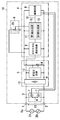
- a light control device of the present invention includes first and second terminals (1, 2), a switch unit (3), an adjustment unit (6), a control unit (4), and a power supply unit (5).
- the first and second terminals (1, 2) are configured such that a series circuit of an AC power supply (30) and a lighting load (31) is connected between the first and second terminals (1, 2) Ru.
- the switch unit (3) includes a normally-off switching element (7) connected between the first and second terminals (1, 2).
- the adjustment unit (6) is configured to change the conduction angle of the switch unit (3).
- the control unit (4) is configured to control the switch unit (3), and includes a zero cross detection circuit (9), a control circuit (11), and a drive circuit (8).
- the zero crossing detection circuit (9) is configured to detect the zero crossing of the AC voltage from the AC power supply (30) when the series circuit is connected between the first and second terminals (1, 2).
- the control circuit (11) is configured to generate a PWM signal (S1) of an on-duty ratio corresponding to the conduction angle obtained from the adjustment unit (6).
- the drive circuit (8) is configured to turn on and off the switching element (7) according to the PWM signal (S1).
- the power supply unit (5) is connected between the first and second terminals (1, 2) and configured to supply power to the control unit (4).
- the control unit (4) controls the switch unit (3) so that the switching element 7 conducts and then shuts off during a variable period shorter than the half cycle of the AC voltage half cycle of the AC power supply (30). Is configured to control.
- the control circuit (11) generates a PWM signal (S1) when a predetermined period (T1) shorter than the variable period elapses from the time when the zero cross of the AC voltage (Va) is detected by the zero cross detection circuit (9). The generation of the pulse for turning on the switching element included is started, and the generation of the pulse is stopped at the end of the variable period.
- the light control device it is possible to maintain the lighting state of the lighting load more stably.
- the dimmer 10 is, for example, a dimmer.
- the dimmer is configured to be attached to a mounting frame (not shown) for the implantable wiring device.
- the light control device 10 is configured to control the first and second terminals 1 and 2, the switch unit 3 electrically connected between the first and second terminals 1 and 2, and the switch unit 3.
- the control unit 4, the power supply unit 5 configured to supply power to the control unit 4, and the adjustment unit 6 configured to vary the conduction angle (phase angle) of the switch unit 3 are provided.
- the conduction angle of the switch unit 3 corresponds to the period in which the switch unit 3 is in the conduction state.
- the power supply unit 5 is electrically connected between the first and second terminals 1 and 2.
- the power supply unit 5 is a constant voltage source.
- a series circuit of the AC power supply 30 and the illumination load 31 can be electrically connected between the first and second terminals 1 and 2.
- the AC power supply 30 is, for example, a commercial power supply, and is used to apply an AC voltage Va to the illumination load 31 via the light control device 10.
- the illumination load 31 is, for example, an LED illumination device.
- the LED lighting device is, for example, an LED bulb.
- the light control device 10 does not include the AC power supply 30 and the illumination load 31 as constituent requirements.
- the LED light bulb is used as an LED lighting apparatus, it does not restrict to this.
- the LED lighting device may be, for example, a downlight, a ceiling light, and the like.
- the switch unit 3 includes a plurality of normally-off switching elements 7 (two in this embodiment).
- Each switching element 7 is, for example, an n-channel MOSFET (Metal Oxide Semiconductor Field Effect Transistor).
- each switching element 7 is connected in reverse series by connecting the source electrodes of each other.
- the light modulation apparatus 10 uses n channel MOSFET as each switching element 7, it does not restrict to this.
- Each switching element 7 may be, for example, an IGBT (Insulated Gate Bipolar Transistor).
- the control unit 4 is configured to drive the illumination load 31 by control similar to reverse phase control by controlling the switch unit 3.
- reverse phase control when the AC voltage Va of the AC power supply 30 is zero, each switching element 7 is switched from the OFF state to the ON state, and when the AC voltage Va of the AC power supply 30 is other than zero, each switching element 7 is ON It means controlling the electric current (electric power supplied to the illumination load 31) which flows into the illumination load 31 by making it from an OFF state.
- each switching element 7 is conducted for a variable period shorter than the start of each AC voltage half cycle and shorter than that half cycle, and the half cycle ends from the end of the variable period. It is cut off until the moment.
- the control unit 4 includes, for example, a microcomputer in which a program is installed.
- the program is stored, for example, in a memory (not shown) provided in advance in a microcomputer.
- the control unit 4 includes a drive circuit 8 configured to drive the two switching elements 7 and a zero cross detection circuit 9 configured to detect a zero cross of the AC voltage Va of the AC power supply 30; And a control circuit 11 configured to supply a Pulse Width Modulation) signal S1 to the drive circuit 8.
- the drive circuit 8 is configured to turn on and off each switching element 7 in accordance with the PWM signal from the control circuit 11. For this reason, the drive circuit 8 is electrically connected to the gate electrode of each switching element 7. Further, the drive circuit 8 is electrically connected to the power supply unit 5. Furthermore, the drive circuit 8 is electrically connected to the source electrode of each switching element 7.
- the zero cross detection circuit 9 is electrically connected to the power supply unit 5. Further, the zero cross detection circuit 9 is electrically connected to the control circuit 11. Furthermore, the zero cross detection circuit 9 is electrically connected to the source electrode of each switching element 7. In short, the zero cross detection circuit 9 is connected between both output terminals of the rectifier circuit 12 and detects the zero cross of the voltage between the output terminals to detect the zero cross of the voltage V1 between the first and second terminals 1 and 2 Do.
- the control circuit 11 is electrically connected to each of the power supply unit 5 and the adjustment unit 6.
- the control circuit 11 is also electrically connected to the drive circuit 8. Furthermore, the control circuit 11 is electrically connected to the source electrode of each switching element 7.
- control unit 4 may include, for example, a control IC (Integrated Circuit).
- control part 4 may be comprised combining a discrete component, for example.
- the power supply unit 5 generates a first DC voltage from the voltage that is full-wave rectified by the rectification circuit 12 configured to full-wave rectify the alternating-current voltage Va of the alternating-current power supply 30, the capacitor 14 and the rectification circuit 12; And a constant voltage circuit configured to apply a first direct current voltage to the capacitor.
- the capacitor 14 is, for example, an electrolytic capacitor.
- the rectifier circuit 12 is, for example, a diode bridge.
- One of the pair of input terminals in the diode bridge is electrically connected to the first terminal (first input terminal) 1, while the other is electrically connected to the second terminal (second input terminal) 2. It is connected.
- One of the pair of output ends (the positive electrode output terminal in the example of FIG. 1) in the diode bridge is electrically connected to the zero cross detection circuit 9.
- the pair of output ends of the diode bridge is electrically connected to the input portion of the constant voltage circuit 13.
- the constant voltage circuit 13 is, for example, a three-terminal regulator.
- the input terminal and the common terminal of the three-terminal regulator are electrically connected to the positive output terminal and the negative output terminal of the diode bridge, respectively.
- the positive electrode and the negative electrode (the positive output terminal and the negative output terminal of the power supply unit 5) of the capacitor 14 are electrically connected to the output terminal and the common terminal (ground terminal) of the three-terminal regulator, respectively. Further, in the present embodiment, the ground terminal of the three-terminal regulator is electrically connected to the source electrode of each switching element 7.
- the light control device 10 uses a three-terminal regulator as the constant voltage circuit 13, the present invention is not limited to this.
- the constant voltage circuit 13 may be, for example, a DC-DC converter.
- the positive electrode of the capacitor 14 is electrically connected to the control unit 4. That is, the control unit 4 is configured to operate with the power from the power supply unit 5 (voltage across the capacitor 14). Specifically, the positive electrode of the capacitor 14 is electrically connected to each of the zero cross detection circuit 9, the control circuit 11, and the drive circuit 8.
- the positive electrode of the capacitor 14 is electrically connected to the adjustment unit 6.
- the adjustment unit 6 includes a variable resistor 20 and an operation unit (not shown) attached to a volume (not shown) of the variable resistor 20.
- the variable resistor 20 is configured to change a resistance value for generating a second DC voltage corresponding to the conduction angle of the switch unit 3.
- the variable resistor 20 is, for example, a potentiometer having three terminals.
- the potentiometer is used as a voltage divider. In the potentiometer, two terminals (hereinafter, first and second terminals) are connected to both ends of the resistive element, and the remaining terminals (hereinafter, third terminal) can be mechanically moved along the resistive element. It is connected to the sliding contact.
- the first terminal of the potentiometer is electrically connected to the positive output terminal of the power supply unit 5 (the positive electrode of the capacitor 14).
- the second terminal of the potentiometer is electrically connected to the negative output terminal of the power supply unit 5 (the source electrode of each switching element 7).
- the third terminal of the potentiometer is electrically connected to the control circuit 11.
- the value (voltage value) of the second DC voltage is set by the resistance value of the variable resistor 20. That is, in the light control device 10, the magnitude of the conduction angle of the switch section 3 is adjusted by the resistance value of the variable resistor 20.
- the plurality of PWM signals S1 that are associated (for example, one to one) with the plurality of second DC voltages and the plurality of second DC voltages are stored in the memory.
- a data table (not shown) including the duty ratio is stored.
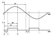
- the on-duty ratio is a ratio of the pulse width (on width) PW to the pulse period PC.
- the pulse cycle PC corresponds to an AC voltage half cycle of the AC power supply 30.
- the apparent pulse period starts at the end time t1 of the predetermined period T1 and ends at the end time of the next predetermined period T1.
- the maximum value among the values of the plurality of second DC voltages corresponds to the maximum value of the second DC voltage varied by the adjustment unit 6, and the minimum value among the values of the plurality of second DC voltages is adjusted by the adjustment unit 6 This corresponds to the minimum value of the second DC voltage to be varied.
- the control circuit 11 is configured to determine the on-duty ratio of the PWM signal S1 corresponding to the value of the second DC voltage from the adjustment unit 6 based on the data table.
- the control circuit 11 is also configured to supply a PWM signal S1 whose on-duty ratio corresponds to the value of the second DC voltage to the drive circuit 8. In short, the control circuit 11 is configured to supply the PWM signal S1 of the on-duty ratio corresponding to the conduction angle of the switch unit 3 set by the adjustment unit 6 to the drive circuit 8.
- the resistance value of the variable resistor 20 is changed by operating the operation unit.
- the magnitude of the conduction angle of the switch unit 3 is changed by operating the operation unit.
- variable resistor 20 may be, for example, a linear potentiometer.
- the control circuit 11 is supplied to the drive circuit 8 when a predetermined period T1 has elapsed from the time when the zero cross of the AC voltage Va of the AC power supply 30 is detected by the zero cross detection circuit 9 (time of t0 in FIG. 2). It is configured to start generation of a pulse for turning on the switching elements 7 and 7 included in the power PWM signal S1.
- the pulse is a rectangular pulse
- the control circuit 11 is configured to raise the pulse when a predetermined period T1 elapses.
- Va on the vertical axis in FIG. 2 represents the AC voltage of the AC power supply 30.
- S1 on the vertical axis in FIG. 2 represents a PWM signal from the control circuit 11.
- Each horizontal axis in FIG. 2 represents time.
- T1 in FIG. 2 represents a point in time when the switch unit 3 is switched from the disconnection state to the conduction state.
- T2 in FIG. 2 represents a point in time when the switch unit 3 is switched from the conduction state to the disconnection state.
- the predetermined period T1 corresponds to a period in which the capacitor 14 is charged to the potential difference of the first DC voltage (charging period of the capacitor 14). Further, the predetermined period T1 is set so as to suppress the generation of noise (switching noise) from the switch unit 3 when the switch unit 3 is switched from the cutoff state to the conductive state. Specifically, when the current flowing to the illumination load 31 is small, the predetermined period T1 is set so that the switch unit 3 changes from the cutoff state to the conduction state.
- the switch unit 3 is switched from the disconnection state to the conduction state. That is, in the light control device 10, when the absolute value of the AC voltage Va of the AC power supply 30 is other than zero, the switch unit 3 is switched from the disconnection state to the conduction state. Thereby, in the light control device 10, the capacitor 14 is charged to the potential difference of the first DC voltage until the predetermined period T1 elapses from the time when the AC voltage Va of the AC power supply 30 crosses zero.
- the light control device 10 when the switch unit 3 is switched from the blocking state to the conductive state, the operation of the control unit 4 can be stabilized as compared with the light control device described in the document 1.
- the light control device 10 can maintain the lighting state of the illumination load 31 more stably than the light control device of Document 1.
- the types of the illumination load 31 that can maintain the lighting state can be increased. Is possible.
- the control circuit 11 comprises a first detection circuit 18 configured to detect a first DC voltage from the power supply 5. When the value of the first DC voltage detected by the first detection circuit 18 is less than or equal to a predetermined first threshold, the control circuit 11 determines that the first DC voltage is greater than the first threshold for a predetermined period T1. It is preferable to make it longer than the predetermined period T1 in the case. In other words, the predetermined period is one of the first and second periods for the first DC voltage, and the first period is longer than the second period.
- the control circuit 11 uses the first period as the predetermined period T1 when the value of the first DC voltage is equal to or less than the first threshold, and sets the first period as the predetermined period T1 when the value of the first DC voltage is larger than the first threshold. Use 2 periods.
- the control unit 4 can monitor the first DC voltage from the power supply unit 5, and the operation of the control unit 4 can be further stabilized.
- the first threshold may be stored in the memory, for example.
- the control circuit 11 also includes a second detection circuit 19 configured to detect the second DC voltage set by the variable resistor 20.
- a second detection circuit 19 configured to detect the second DC voltage set by the variable resistor 20.
- the control circuit 11 determines that the predetermined DC voltage value is larger than the second threshold value for a predetermined period T1. It is preferable to make it shorter than the predetermined period T1 in the case.
- the predetermined period is one of the first and second periods for the second DC voltage, and the first period for the second DC voltage is shorter than the second period for the second DC voltage.
- the control circuit 11 uses the first period for the second DC voltage as the predetermined period T1, and the value of the second DC voltage is larger than the second threshold.
- the second period for the second DC voltage is used as the predetermined period T1.
- the lighting load 31 may be, for example, an incandescent lamp.
- the incandescent bulb may be, for example, a halogen bulb, a krypton bulb or the like.
- the light control apparatus 10 of the present embodiment described above includes the first and second terminals 1 and 2, the switch unit 3, the adjustment unit 6, the control unit 4, and the power supply unit 5.
- the first and second terminals 1 and 2 are configured such that a series circuit of the AC power supply 30 and the lighting load 31 is connected between the first and second terminals 1 and 2.
- the switch unit 3 includes a (at least one) normally-off switching element 7 connected between the first and second terminals 1 and 2.
- the adjustment unit 6 is configured to change the conduction angle of the switch unit 3.
- the control unit 4 is configured to control the switch unit 3, and includes a zero cross detection circuit 9, a control circuit 11, and a drive circuit 8.
- the zero cross detection circuit 9 is configured to detect the zero cross of the AC voltage Va from the AC power supply 30 when the series circuit is connected between the first and second terminals 1 and 2.
- the control circuit 11 is configured to generate a PWM signal S1 of an on-duty ratio (PW / PC) corresponding to the conduction angle obtained from the adjustment unit 6.
- the drive circuit 8 is configured to turn on and off the switching element 7 in accordance with the PWM signal S1.
- the power supply unit 5 is connected between the first and second terminals 1 and 2 and configured to supply power to the control unit 4.
- Control unit 4 performs a switch so that switching element 7 conducts and then shuts off during the variable period VP shorter than the half cycle of the AC voltage half cycle of AC power supply 30 (see PC in FIG. 2). It is configured to control the unit 3.
- the control circuit 11 sets the switching element 7 included in the PWM signal S1 at time t1 when a predetermined period T1 shorter than the variable period VP has elapsed from time t0 when the zero cross of the AC voltage Va is detected by the zero cross detection circuit 9.
- the generation of a pulse for turning on is started, and the generation of the pulse is stopped at the end time t2 of the variable period VP.
- the control circuit 11 is configured to cause the pulse to fall at the end time t2 of the variable period VP.
- the control circuit 11 comprises a first detection circuit 18 configured to detect the voltage from the power supply 5.
- the predetermined period is one of a first period and a second period, and the first period is longer than the second period.
- the control circuit 11 is included in the PWM signal S1 when the first period as the predetermined period T1 elapses when the value of the voltage detected by the first detection circuit 18 is equal to or less than a preset first threshold. It is configured to start the generation of a pulse.
- the control circuit 11 is configured to stop the generation of the pulse included in the PWM signal S1 when the second period as the predetermined period elapses when the value of the voltage is larger than the first threshold. Ru.
- the control unit 4 can monitor the first DC voltage from the power supply unit 5, and the operation of the control unit 4 can be further stabilized.
- the power supply unit 5 generates a first DC voltage from the voltage that is full-wave rectified by the rectification circuit 12 configured to full-wave rectify the AC voltage Va, the capacitor 14 and the rectification circuit 12 And a constant voltage circuit 13 configured to apply the first DC voltage to the capacitor 14.
- the first detection circuit 18 is configured to detect the voltage across the capacitor 14.
- the adjustment unit 6 includes a variable resistor 20 that changes a resistance value for generating a second DC voltage corresponding to the conduction angle of the switch unit 3.
- the control circuit 11 comprises a second detection circuit 19 configured to detect the second DC voltage generated by the variable resistor 20.
- the predetermined period is one of a first period and a second period, and the first period is shorter than the second period.
- the control circuit 11 outputs the PWM signal S1 to the PWM signal S1 when the first period as the predetermined period T1 has elapsed. It is configured to start the generation of the included pulse.
- the control circuit 11 stops the generation of the pulse included in the PWM signal S1 when the second period as the predetermined period T1 elapses.
- the predetermined period T1 in accordance with the light control level of the illumination load 31.
- the predetermined period T1 can be shorter than the predetermined period T1 in the case where the light control level of the illumination load 31 is high.
- the predetermined period T1 in the case where the light control level of the illumination load 31 is high.
- noise reduction can be achieved as compared with the case where the light control level of the illumination load 31 is high.
Abstract
L'invention concerne un dispositif gradateur de lumière (10) qui comporte des première et seconde bornes (1 et 2), une unité de commutation (3) comprenant des éléments de commutation (7) connectée entre lesdites première et seconde bornes (1 et 2), une unité de réglage (6) qui peut changer l'angle de conduction de l'unité de commutation (3), une unité de commande (4) qui commande l'unité de commutation (3), et une unité d'alimentation (5) qui alimente électriquement l'unité de commande (4). L'unité de commande (4) comprend un circuit de détection de passage par le point zéro (9) qui détecte des passages par le point zéro d'une tension alternative (Va), un circuit de commande (11) qui génère un signal PWM ayant un rapport cyclique correspondant à l'angle de conduction obtenu à partir de l'unité d'ajustement (6), et un circuit d'attaque (8) qui utilise ledit signal PWM pour attaquer les éléments de commutation (7). L'unité de commande (4) débloque les éléments de commutation (7) et les bloque ensuite durant une période de changement qui commence au début d'un demi-cycle de la tension alternative et est plus courte que ledit demi-cycle. Le circuit de commande (11) commence à générer les impulsions constituant le signal PWM lorsqu'une durée prescrite qui est plus courte que la période de changement susmentionnée s'est écoulée à partir d'un passage par le point zéro de la tension alternative (Va).
Priority Applications (4)
| Application Number | Priority Date | Filing Date | Title |
|---|---|---|---|
| EP18200433.3A EP3468308A1 (fr) | 2014-04-03 | 2015-03-26 | Dispositif de gradation de lumière |
| EP15772388.3A EP3128814B1 (fr) | 2014-04-03 | 2015-03-26 | Dispositif gradateur de lumière |
| CN201580017782.2A CN106165547B (zh) | 2014-04-03 | 2015-03-26 | 调光装置 |
| US15/300,065 US9974134B2 (en) | 2014-04-03 | 2015-03-26 | Light-dimming device |
Applications Claiming Priority (2)
| Application Number | Priority Date | Filing Date | Title |
|---|---|---|---|
| JP2014-077193 | 2014-04-03 | ||
| JP2014077193A JP6195199B2 (ja) | 2014-04-03 | 2014-04-03 | 調光装置 |
Publications (1)
| Publication Number | Publication Date |
|---|---|
| WO2015151464A1 true WO2015151464A1 (fr) | 2015-10-08 |
Family
ID=54239811
Family Applications (1)
| Application Number | Title | Priority Date | Filing Date |
|---|---|---|---|
| PCT/JP2015/001710 WO2015151464A1 (fr) | 2014-04-03 | 2015-03-26 | Dispositif gradateur de lumière |
Country Status (6)
| Country | Link |
|---|---|
| US (1) | US9974134B2 (fr) |
| EP (2) | EP3128814B1 (fr) |
| JP (1) | JP6195199B2 (fr) |
| CN (1) | CN106165547B (fr) |
| TW (2) | TWI583252B (fr) |
| WO (1) | WO2015151464A1 (fr) |
Cited By (1)
| Publication number | Priority date | Publication date | Assignee | Title |
|---|---|---|---|---|
| CN105813260A (zh) * | 2016-04-01 | 2016-07-27 | 温州沃斯托科技有限公司 | 二线型后切调节器及调节方法 |
Families Citing this family (8)
| Publication number | Priority date | Publication date | Assignee | Title |
|---|---|---|---|---|
| JP6195199B2 (ja) * | 2014-04-03 | 2017-09-13 | パナソニックIpマネジメント株式会社 | 調光装置 |
| JP6195200B2 (ja) * | 2014-04-03 | 2017-09-13 | パナソニックIpマネジメント株式会社 | 調光装置 |
| TWI589181B (zh) * | 2016-02-02 | 2017-06-21 | 隆達電子股份有限公司 | 調光模組以及固態光源裝置 |
| CA2950054A1 (fr) * | 2016-11-30 | 2018-05-30 | Technologies Intelia Inc. | Methode et systeme pour gradateur de lumiere sans scintillement sur un reseau d'alimentation alternatif |
| CN108599108B (zh) * | 2018-04-30 | 2023-11-17 | 上海晶丰明源半导体股份有限公司 | 保护电路、驱动系统、芯片及电路保护方法、驱动方法 |
| CN109246885B (zh) * | 2018-09-11 | 2020-12-18 | 莱昊(上海)光电科技有限公司 | 一种led的切相调光装置 |
| CN112444721B (zh) * | 2019-08-30 | 2024-03-29 | 宁德时代新能源科技股份有限公司 | 一种电控制器件的检测电路及检测方法 |
| CN111295016A (zh) * | 2020-02-19 | 2020-06-16 | 杭州涂鸦信息技术有限公司 | 一种单火线调光装置的调光方法及系统 |
Citations (5)
| Publication number | Priority date | Publication date | Assignee | Title |
|---|---|---|---|---|
| JPH11161347A (ja) * | 1997-11-28 | 1999-06-18 | Matsushita Electric Works Ltd | 位相制御装置の制御回路 |
| JP2011050149A (ja) * | 2009-08-26 | 2011-03-10 | Panasonic Electric Works Co Ltd | 負荷制御装置 |
| JP2011238353A (ja) * | 2010-04-30 | 2011-11-24 | Jimbo Electric Co Ltd | 2線式逆位相制御装置 |
| JP2013004350A (ja) * | 2011-06-17 | 2013-01-07 | Toshiba Lighting & Technology Corp | 逆位相制御装置 |
| JP2013149498A (ja) * | 2012-01-19 | 2013-08-01 | Toshiba Lighting & Technology Corp | 調光装置 |
Family Cites Families (30)
| Publication number | Priority date | Publication date | Assignee | Title |
|---|---|---|---|---|
| TWI252060B (en) * | 2003-06-27 | 2006-03-21 | Matsushita Electric Works Ltd | Phase controller |
| JP2007080771A (ja) * | 2005-09-16 | 2007-03-29 | Nec Lighting Ltd | 照明用低圧電源回路、照明装置および照明用低圧電源出力方法 |
| JP4979301B2 (ja) | 2006-08-07 | 2012-07-18 | 神保電器株式会社 | 位相制御装置及び位相制御方法 |
| US7667408B2 (en) * | 2007-03-12 | 2010-02-23 | Cirrus Logic, Inc. | Lighting system with lighting dimmer output mapping |
| JP5294903B2 (ja) * | 2008-08-21 | 2013-09-18 | パナソニック株式会社 | 負荷制御装置及びそれを備えた負荷制御システム |
| CN101951708B (zh) * | 2009-07-10 | 2013-09-18 | 深圳比亚迪微电子有限公司 | 调光控制电路、芯片及方法 |
| JP5362484B2 (ja) * | 2009-08-26 | 2013-12-11 | パナソニック株式会社 | 負荷制御装置 |
| CN102576233B (zh) * | 2009-08-26 | 2014-11-26 | 松下电器产业株式会社 | 负载控制装置 |
| TWI461095B (zh) * | 2009-11-19 | 2014-11-11 | Huizhou Light Engine Ltd | 用以控制發光二極體之亮度的方法及裝置 |
| US8242766B2 (en) * | 2010-04-20 | 2012-08-14 | Power Integrations, Inc. | Dimming control for a switching power supply |
| CN101835314B (zh) * | 2010-05-19 | 2013-12-04 | 成都芯源系统有限公司 | 一种具有调光功能的led驱动电路及灯具 |
| US8310163B2 (en) * | 2010-08-24 | 2012-11-13 | Chia-Teh Chen | Microcontroller-based lighting control system and method for lighting control |
| US9084316B2 (en) * | 2010-11-04 | 2015-07-14 | Cirrus Logic, Inc. | Controlled power dissipation in a switch path in a lighting system |
| CN103201937B (zh) * | 2010-11-04 | 2017-02-15 | 皇家飞利浦有限公司 | 用于控制照明系统中的功率消耗的装置和方法 |
| US8618743B2 (en) * | 2010-12-14 | 2013-12-31 | Elm Inc. | High stability dimmer |
| CN102769960A (zh) * | 2011-05-06 | 2012-11-07 | 欧司朗股份有限公司 | 可调光led驱动器及其控制方法 |
| EP2715924A1 (fr) * | 2011-06-03 | 2014-04-09 | Cirrus Logic, Inc. | Détermination de données de commande à partir d'une détection côté primaire d'une tension côté secondaire dans un convertisseur de puissance de commutation |
| CN102958218B (zh) * | 2011-08-17 | 2015-01-14 | 浙江英飞特节能技术有限公司 | 光源控制方法、装置及系统 |
| JP5870292B2 (ja) | 2011-11-22 | 2016-02-24 | パナソニックIpマネジメント株式会社 | 調光器 |
| US9307588B2 (en) * | 2012-12-17 | 2016-04-05 | Ecosense Lighting Inc. | Systems and methods for dimming of a light source |
| JP6176567B2 (ja) * | 2013-07-09 | 2017-08-09 | パナソニックIpマネジメント株式会社 | 点灯装置 |
| CN103415111B (zh) * | 2013-07-30 | 2016-06-22 | 浙江生辉照明有限公司 | Led照明装置的驱动电路及驱动方法 |
| JP6369780B2 (ja) * | 2013-10-01 | 2018-08-08 | パナソニックIpマネジメント株式会社 | 点灯装置、照明装置、照明器具、及び照明システム |
| US9473031B2 (en) * | 2014-01-13 | 2016-10-18 | Power Integrations, Inc. | Variable feedback signal based on conduction time |
| JP6372776B2 (ja) * | 2014-03-07 | 2018-08-15 | パナソニックIpマネジメント株式会社 | 光源装置及び点灯装置、照明器具 |
| US20170019966A1 (en) * | 2014-03-11 | 2017-01-19 | Panasonic Intellectual Property Management Co., Ltd. | Dimming device |
| JP6195200B2 (ja) * | 2014-04-03 | 2017-09-13 | パナソニックIpマネジメント株式会社 | 調光装置 |
| JP6195199B2 (ja) * | 2014-04-03 | 2017-09-13 | パナソニックIpマネジメント株式会社 | 調光装置 |
| US9215772B2 (en) * | 2014-04-17 | 2015-12-15 | Philips International B.V. | Systems and methods for minimizing power dissipation in a low-power lamp coupled to a trailing-edge dimmer |
| JP6551735B2 (ja) * | 2015-06-09 | 2019-07-31 | パナソニックIpマネジメント株式会社 | 調光点灯回路及び照明器具 |
-
2014
- 2014-04-03 JP JP2014077193A patent/JP6195199B2/ja active Active
-
2015
- 2015-03-26 CN CN201580017782.2A patent/CN106165547B/zh active Active
- 2015-03-26 WO PCT/JP2015/001710 patent/WO2015151464A1/fr active Application Filing
- 2015-03-26 EP EP15772388.3A patent/EP3128814B1/fr active Active
- 2015-03-26 EP EP18200433.3A patent/EP3468308A1/fr not_active Withdrawn
- 2015-03-26 US US15/300,065 patent/US9974134B2/en active Active
- 2015-03-27 TW TW105130434A patent/TWI583252B/zh active
- 2015-03-27 TW TW104109910A patent/TWI561109B/zh active
Patent Citations (5)
| Publication number | Priority date | Publication date | Assignee | Title |
|---|---|---|---|---|
| JPH11161347A (ja) * | 1997-11-28 | 1999-06-18 | Matsushita Electric Works Ltd | 位相制御装置の制御回路 |
| JP2011050149A (ja) * | 2009-08-26 | 2011-03-10 | Panasonic Electric Works Co Ltd | 負荷制御装置 |
| JP2011238353A (ja) * | 2010-04-30 | 2011-11-24 | Jimbo Electric Co Ltd | 2線式逆位相制御装置 |
| JP2013004350A (ja) * | 2011-06-17 | 2013-01-07 | Toshiba Lighting & Technology Corp | 逆位相制御装置 |
| JP2013149498A (ja) * | 2012-01-19 | 2013-08-01 | Toshiba Lighting & Technology Corp | 調光装置 |
Cited By (1)
| Publication number | Priority date | Publication date | Assignee | Title |
|---|---|---|---|---|
| CN105813260A (zh) * | 2016-04-01 | 2016-07-27 | 温州沃斯托科技有限公司 | 二线型后切调节器及调节方法 |
Also Published As
| Publication number | Publication date |
|---|---|
| EP3128814A1 (fr) | 2017-02-08 |
| CN106165547B (zh) | 2018-12-25 |
| US9974134B2 (en) | 2018-05-15 |
| EP3468308A1 (fr) | 2019-04-10 |
| TWI583252B (zh) | 2017-05-11 |
| US20170150568A1 (en) | 2017-05-25 |
| CN106165547A (zh) | 2016-11-23 |
| TW201605290A (zh) | 2016-02-01 |
| TW201701726A (zh) | 2017-01-01 |
| JP6195199B2 (ja) | 2017-09-13 |
| TWI561109B (en) | 2016-12-01 |
| JP2015198074A (ja) | 2015-11-09 |
| EP3128814B1 (fr) | 2018-11-28 |
| EP3128814A4 (fr) | 2017-04-26 |
Similar Documents
| Publication | Publication Date | Title |
|---|---|---|
| WO2015151464A1 (fr) | Dispositif gradateur de lumière | |
| TWI544835B (zh) | 調光裝置 | |
| CN104041188B (zh) | 双线式调光开关 | |
| JP6811386B2 (ja) | 調光装置 | |
| CN108243545B (zh) | 负载控制装置 | |
| JP6534102B2 (ja) | 調光装置 | |
| TWI584693B (zh) | Dimming device | |
| JP5528883B2 (ja) | Led駆動回路 | |
| WO2018055990A1 (fr) | Circuit de protection pour dispositif de réglage de lumière, et dispositif de réglage de lumière | |
| JP5967513B2 (ja) | 調光器 | |
| JP6618014B2 (ja) | 調光装置及び照明制御システム | |
| JP5669447B2 (ja) | 照明システム | |
| CN108029183B (zh) | 调光装置 | |
| AU2003292284A1 (en) | Power controller | |
| JP2020077503A (ja) | 点灯システム、照明制御システム、及び照明器具 | |
| JP2020077504A (ja) | 点灯システム、照明制御システム、及び照明器具 |
Legal Events
| Date | Code | Title | Description |
|---|---|---|---|
| 121 | Ep: the epo has been informed by wipo that ep was designated in this application |
Ref document number: 15772388 Country of ref document: EP Kind code of ref document: A1 |
|
| WWE | Wipo information: entry into national phase |
Ref document number: 15300065 Country of ref document: US |
|
| NENP | Non-entry into the national phase |
Ref country code: DE |
|
| REEP | Request for entry into the european phase |
Ref document number: 2015772388 Country of ref document: EP |
|
| WWE | Wipo information: entry into national phase |
Ref document number: 2015772388 Country of ref document: EP |