WO2015151464A1 - Light-dimming device - Google Patents
Light-dimming device Download PDFInfo
- Publication number
- WO2015151464A1 WO2015151464A1 PCT/JP2015/001710 JP2015001710W WO2015151464A1 WO 2015151464 A1 WO2015151464 A1 WO 2015151464A1 JP 2015001710 W JP2015001710 W JP 2015001710W WO 2015151464 A1 WO2015151464 A1 WO 2015151464A1
- Authority
- WO
- WIPO (PCT)
- Prior art keywords
- voltage
- period
- unit
- circuit
- power supply
- Prior art date
Links
Images
Classifications
-
- H—ELECTRICITY
- H05—ELECTRIC TECHNIQUES NOT OTHERWISE PROVIDED FOR
- H05B—ELECTRIC HEATING; ELECTRIC LIGHT SOURCES NOT OTHERWISE PROVIDED FOR; CIRCUIT ARRANGEMENTS FOR ELECTRIC LIGHT SOURCES, IN GENERAL
- H05B45/00—Circuit arrangements for operating light-emitting diodes [LED]
- H05B45/10—Controlling the intensity of the light
-
- H—ELECTRICITY
- H02—GENERATION; CONVERSION OR DISTRIBUTION OF ELECTRIC POWER
- H02M—APPARATUS FOR CONVERSION BETWEEN AC AND AC, BETWEEN AC AND DC, OR BETWEEN DC AND DC, AND FOR USE WITH MAINS OR SIMILAR POWER SUPPLY SYSTEMS; CONVERSION OF DC OR AC INPUT POWER INTO SURGE OUTPUT POWER; CONTROL OR REGULATION THEREOF
- H02M1/00—Details of apparatus for conversion
- H02M1/08—Circuits specially adapted for the generation of control voltages for semiconductor devices incorporated in static converters
-
- H—ELECTRICITY
- H02—GENERATION; CONVERSION OR DISTRIBUTION OF ELECTRIC POWER
- H02M—APPARATUS FOR CONVERSION BETWEEN AC AND AC, BETWEEN AC AND DC, OR BETWEEN DC AND DC, AND FOR USE WITH MAINS OR SIMILAR POWER SUPPLY SYSTEMS; CONVERSION OF DC OR AC INPUT POWER INTO SURGE OUTPUT POWER; CONTROL OR REGULATION THEREOF
- H02M1/00—Details of apparatus for conversion
- H02M1/36—Means for starting or stopping converters
-
- H—ELECTRICITY
- H03—ELECTRONIC CIRCUITRY
- H03K—PULSE TECHNIQUE
- H03K17/00—Electronic switching or gating, i.e. not by contact-making and –breaking
- H03K17/51—Electronic switching or gating, i.e. not by contact-making and –breaking characterised by the components used
- H03K17/56—Electronic switching or gating, i.e. not by contact-making and –breaking characterised by the components used by the use, as active elements, of semiconductor devices
- H03K17/72—Electronic switching or gating, i.e. not by contact-making and –breaking characterised by the components used by the use, as active elements, of semiconductor devices having more than two PN junctions; having more than three electrodes; having more than one electrode connected to the same conductivity region
- H03K17/725—Electronic switching or gating, i.e. not by contact-making and –breaking characterised by the components used by the use, as active elements, of semiconductor devices having more than two PN junctions; having more than three electrodes; having more than one electrode connected to the same conductivity region for ac voltages or currents
-
- H—ELECTRICITY
- H05—ELECTRIC TECHNIQUES NOT OTHERWISE PROVIDED FOR
- H05B—ELECTRIC HEATING; ELECTRIC LIGHT SOURCES NOT OTHERWISE PROVIDED FOR; CIRCUIT ARRANGEMENTS FOR ELECTRIC LIGHT SOURCES, IN GENERAL
- H05B39/00—Circuit arrangements or apparatus for operating incandescent light sources
- H05B39/04—Controlling
- H05B39/041—Controlling the light-intensity of the source
- H05B39/044—Controlling the light-intensity of the source continuously
- H05B39/048—Controlling the light-intensity of the source continuously with reverse phase control
-
- H—ELECTRICITY
- H05—ELECTRIC TECHNIQUES NOT OTHERWISE PROVIDED FOR
- H05B—ELECTRIC HEATING; ELECTRIC LIGHT SOURCES NOT OTHERWISE PROVIDED FOR; CIRCUIT ARRANGEMENTS FOR ELECTRIC LIGHT SOURCES, IN GENERAL
- H05B45/00—Circuit arrangements for operating light-emitting diodes [LED]
- H05B45/30—Driver circuits
- H05B45/37—Converter circuits
- H05B45/3725—Switched mode power supply [SMPS]
-
- Y—GENERAL TAGGING OF NEW TECHNOLOGICAL DEVELOPMENTS; GENERAL TAGGING OF CROSS-SECTIONAL TECHNOLOGIES SPANNING OVER SEVERAL SECTIONS OF THE IPC; TECHNICAL SUBJECTS COVERED BY FORMER USPC CROSS-REFERENCE ART COLLECTIONS [XRACs] AND DIGESTS
- Y02—TECHNOLOGIES OR APPLICATIONS FOR MITIGATION OR ADAPTATION AGAINST CLIMATE CHANGE
- Y02B—CLIMATE CHANGE MITIGATION TECHNOLOGIES RELATED TO BUILDINGS, e.g. HOUSING, HOUSE APPLIANCES OR RELATED END-USER APPLICATIONS
- Y02B20/00—Energy efficient lighting technologies, e.g. halogen lamps or gas discharge lamps
Definitions
- the present invention relates to a dimming device configured to dim a lighting load, ie to adjust the light output of the lighting load.
- the light control apparatus described in Document 1 includes a pair of terminals, a control circuit unit, a control power supply unit that supplies control power to the control circuit unit, and a light control unit that sets a light control level of the illumination load. Have.
- the control circuit unit and the control power supply unit are connected in parallel between the pair of terminals.
- a series circuit of an AC power supply and a lighting load is connected between the pair of terminals.
- the lighting load includes a plurality of LED (Light Emitting Diode) elements and a power supply circuit for lighting each LED element.
- the power supply circuit includes a smoothing circuit of a diode and an electrolytic capacitor.
- the control circuit unit includes a switch unit that performs phase control of an AC voltage supplied to the illumination load, a switch drive unit that drives the switch unit, and a control unit that controls the switch drive unit and the control power supply unit.
- the control power supply unit is connected in parallel to the switch unit.
- the control power supply unit converts an AC voltage of the AC power supply into a control power supply.
- the control power supply unit includes an electrolytic capacitor that stores the control power supply.
- the control unit is supplied with control power from the control power unit through the electrolytic capacitor.
- the control unit includes a microcomputer.
- the microcomputer performs reverse phase control to cut off the power supply to the illumination load in the middle of each half cycle of the AC voltage according to the light control level set by the light control unit.
- Document 2 Japanese Patent Application Publication No. 2011-238353
- the two-wire antiphase control device described in Document 2 includes a main current switching circuit, a dimming variable pulse delay circuit, and a DC power supply generation circuit.
- the main current switching circuit comprises a main current circuit and two MOSFETs connected in reverse series.
- the two MOSFETs are connected in parallel with a series circuit of an AC power supply and a lighting load.
- the dimming variable pulse delay circuit is configured to determine the timing for discharging the gate charge of each MOSFET.
- the DC power supply generation circuit is configured by an integration circuit of a resistor and a capacitor. Further, the DC power supply generation circuit is configured to supply the DC power generated at the voltage across the capacitor to the dimming variable pulse delay circuit.
- the microcomputer of the control unit in the light control apparatus described in Document 1 performs reverse phase control of the illumination load. Therefore, in the light control device, when the absolute value of the alternating current voltage of the alternating current power supply is other than zero, the switch unit changes from the conductive state to the cut off state, and a predetermined period of the period from the cut off state to the conductive state The control power is accumulated in the electrolytic capacitor of the control power unit. Further, in the two-wire antiphase control device described in Document 2, the capacitors of the DC power supply generation circuit are charged in the entire period from when each MOSFET is turned off to when it becomes conductive.
- the illumination load is provided with the smoothing circuit.
- current may not flow to the lighting load, and the control capacitor may not be sufficiently accumulated in the electrolytic capacitor.
- the operation of controlling the switching drive unit by the control unit may become unstable, and the lighting state of the illumination load may not be maintained.
- the object of the present invention is to provide a dimmer capable of maintaining the lighting state of the lighting load more stably.
- a light control device of the present invention includes first and second terminals (1, 2), a switch unit (3), an adjustment unit (6), a control unit (4), and a power supply unit (5).
- the first and second terminals (1, 2) are configured such that a series circuit of an AC power supply (30) and a lighting load (31) is connected between the first and second terminals (1, 2) Ru.
- the switch unit (3) includes a normally-off switching element (7) connected between the first and second terminals (1, 2).
- the adjustment unit (6) is configured to change the conduction angle of the switch unit (3).
- the control unit (4) is configured to control the switch unit (3), and includes a zero cross detection circuit (9), a control circuit (11), and a drive circuit (8).
- the zero crossing detection circuit (9) is configured to detect the zero crossing of the AC voltage from the AC power supply (30) when the series circuit is connected between the first and second terminals (1, 2).
- the control circuit (11) is configured to generate a PWM signal (S1) of an on-duty ratio corresponding to the conduction angle obtained from the adjustment unit (6).
- the drive circuit (8) is configured to turn on and off the switching element (7) according to the PWM signal (S1).
- the power supply unit (5) is connected between the first and second terminals (1, 2) and configured to supply power to the control unit (4).
- the control unit (4) controls the switch unit (3) so that the switching element 7 conducts and then shuts off during a variable period shorter than the half cycle of the AC voltage half cycle of the AC power supply (30). Is configured to control.
- the control circuit (11) generates a PWM signal (S1) when a predetermined period (T1) shorter than the variable period elapses from the time when the zero cross of the AC voltage (Va) is detected by the zero cross detection circuit (9). The generation of the pulse for turning on the switching element included is started, and the generation of the pulse is stopped at the end of the variable period.
- the light control device it is possible to maintain the lighting state of the lighting load more stably.
- the dimmer 10 is, for example, a dimmer.
- the dimmer is configured to be attached to a mounting frame (not shown) for the implantable wiring device.
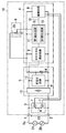
- the light control device 10 is configured to control the first and second terminals 1 and 2, the switch unit 3 electrically connected between the first and second terminals 1 and 2, and the switch unit 3.
- the control unit 4, the power supply unit 5 configured to supply power to the control unit 4, and the adjustment unit 6 configured to vary the conduction angle (phase angle) of the switch unit 3 are provided.
- the conduction angle of the switch unit 3 corresponds to the period in which the switch unit 3 is in the conduction state.
- the power supply unit 5 is electrically connected between the first and second terminals 1 and 2.
- the power supply unit 5 is a constant voltage source.
- a series circuit of the AC power supply 30 and the illumination load 31 can be electrically connected between the first and second terminals 1 and 2.
- the AC power supply 30 is, for example, a commercial power supply, and is used to apply an AC voltage Va to the illumination load 31 via the light control device 10.
- the illumination load 31 is, for example, an LED illumination device.
- the LED lighting device is, for example, an LED bulb.
- the light control device 10 does not include the AC power supply 30 and the illumination load 31 as constituent requirements.
- the LED light bulb is used as an LED lighting apparatus, it does not restrict to this.
- the LED lighting device may be, for example, a downlight, a ceiling light, and the like.
- the switch unit 3 includes a plurality of normally-off switching elements 7 (two in this embodiment).
- Each switching element 7 is, for example, an n-channel MOSFET (Metal Oxide Semiconductor Field Effect Transistor).
- each switching element 7 is connected in reverse series by connecting the source electrodes of each other.
- the light modulation apparatus 10 uses n channel MOSFET as each switching element 7, it does not restrict to this.
- Each switching element 7 may be, for example, an IGBT (Insulated Gate Bipolar Transistor).
- the control unit 4 is configured to drive the illumination load 31 by control similar to reverse phase control by controlling the switch unit 3.
- reverse phase control when the AC voltage Va of the AC power supply 30 is zero, each switching element 7 is switched from the OFF state to the ON state, and when the AC voltage Va of the AC power supply 30 is other than zero, each switching element 7 is ON It means controlling the electric current (electric power supplied to the illumination load 31) which flows into the illumination load 31 by making it from an OFF state.
- each switching element 7 is conducted for a variable period shorter than the start of each AC voltage half cycle and shorter than that half cycle, and the half cycle ends from the end of the variable period. It is cut off until the moment.
- the control unit 4 includes, for example, a microcomputer in which a program is installed.
- the program is stored, for example, in a memory (not shown) provided in advance in a microcomputer.
- the control unit 4 includes a drive circuit 8 configured to drive the two switching elements 7 and a zero cross detection circuit 9 configured to detect a zero cross of the AC voltage Va of the AC power supply 30; And a control circuit 11 configured to supply a Pulse Width Modulation) signal S1 to the drive circuit 8.
- the drive circuit 8 is configured to turn on and off each switching element 7 in accordance with the PWM signal from the control circuit 11. For this reason, the drive circuit 8 is electrically connected to the gate electrode of each switching element 7. Further, the drive circuit 8 is electrically connected to the power supply unit 5. Furthermore, the drive circuit 8 is electrically connected to the source electrode of each switching element 7.
- the zero cross detection circuit 9 is electrically connected to the power supply unit 5. Further, the zero cross detection circuit 9 is electrically connected to the control circuit 11. Furthermore, the zero cross detection circuit 9 is electrically connected to the source electrode of each switching element 7. In short, the zero cross detection circuit 9 is connected between both output terminals of the rectifier circuit 12 and detects the zero cross of the voltage between the output terminals to detect the zero cross of the voltage V1 between the first and second terminals 1 and 2 Do.
- the control circuit 11 is electrically connected to each of the power supply unit 5 and the adjustment unit 6.
- the control circuit 11 is also electrically connected to the drive circuit 8. Furthermore, the control circuit 11 is electrically connected to the source electrode of each switching element 7.
- control unit 4 may include, for example, a control IC (Integrated Circuit).
- control part 4 may be comprised combining a discrete component, for example.
- the power supply unit 5 generates a first DC voltage from the voltage that is full-wave rectified by the rectification circuit 12 configured to full-wave rectify the alternating-current voltage Va of the alternating-current power supply 30, the capacitor 14 and the rectification circuit 12; And a constant voltage circuit configured to apply a first direct current voltage to the capacitor.
- the capacitor 14 is, for example, an electrolytic capacitor.
- the rectifier circuit 12 is, for example, a diode bridge.
- One of the pair of input terminals in the diode bridge is electrically connected to the first terminal (first input terminal) 1, while the other is electrically connected to the second terminal (second input terminal) 2. It is connected.
- One of the pair of output ends (the positive electrode output terminal in the example of FIG. 1) in the diode bridge is electrically connected to the zero cross detection circuit 9.
- the pair of output ends of the diode bridge is electrically connected to the input portion of the constant voltage circuit 13.
- the constant voltage circuit 13 is, for example, a three-terminal regulator.
- the input terminal and the common terminal of the three-terminal regulator are electrically connected to the positive output terminal and the negative output terminal of the diode bridge, respectively.
- the positive electrode and the negative electrode (the positive output terminal and the negative output terminal of the power supply unit 5) of the capacitor 14 are electrically connected to the output terminal and the common terminal (ground terminal) of the three-terminal regulator, respectively. Further, in the present embodiment, the ground terminal of the three-terminal regulator is electrically connected to the source electrode of each switching element 7.
- the light control device 10 uses a three-terminal regulator as the constant voltage circuit 13, the present invention is not limited to this.
- the constant voltage circuit 13 may be, for example, a DC-DC converter.
- the positive electrode of the capacitor 14 is electrically connected to the control unit 4. That is, the control unit 4 is configured to operate with the power from the power supply unit 5 (voltage across the capacitor 14). Specifically, the positive electrode of the capacitor 14 is electrically connected to each of the zero cross detection circuit 9, the control circuit 11, and the drive circuit 8.
- the positive electrode of the capacitor 14 is electrically connected to the adjustment unit 6.
- the adjustment unit 6 includes a variable resistor 20 and an operation unit (not shown) attached to a volume (not shown) of the variable resistor 20.
- the variable resistor 20 is configured to change a resistance value for generating a second DC voltage corresponding to the conduction angle of the switch unit 3.
- the variable resistor 20 is, for example, a potentiometer having three terminals.
- the potentiometer is used as a voltage divider. In the potentiometer, two terminals (hereinafter, first and second terminals) are connected to both ends of the resistive element, and the remaining terminals (hereinafter, third terminal) can be mechanically moved along the resistive element. It is connected to the sliding contact.
- the first terminal of the potentiometer is electrically connected to the positive output terminal of the power supply unit 5 (the positive electrode of the capacitor 14).
- the second terminal of the potentiometer is electrically connected to the negative output terminal of the power supply unit 5 (the source electrode of each switching element 7).
- the third terminal of the potentiometer is electrically connected to the control circuit 11.
- the value (voltage value) of the second DC voltage is set by the resistance value of the variable resistor 20. That is, in the light control device 10, the magnitude of the conduction angle of the switch section 3 is adjusted by the resistance value of the variable resistor 20.
- the plurality of PWM signals S1 that are associated (for example, one to one) with the plurality of second DC voltages and the plurality of second DC voltages are stored in the memory.
- a data table (not shown) including the duty ratio is stored.
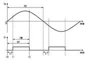
- the on-duty ratio is a ratio of the pulse width (on width) PW to the pulse period PC.
- the pulse cycle PC corresponds to an AC voltage half cycle of the AC power supply 30.
- the apparent pulse period starts at the end time t1 of the predetermined period T1 and ends at the end time of the next predetermined period T1.
- the maximum value among the values of the plurality of second DC voltages corresponds to the maximum value of the second DC voltage varied by the adjustment unit 6, and the minimum value among the values of the plurality of second DC voltages is adjusted by the adjustment unit 6 This corresponds to the minimum value of the second DC voltage to be varied.
- the control circuit 11 is configured to determine the on-duty ratio of the PWM signal S1 corresponding to the value of the second DC voltage from the adjustment unit 6 based on the data table.
- the control circuit 11 is also configured to supply a PWM signal S1 whose on-duty ratio corresponds to the value of the second DC voltage to the drive circuit 8. In short, the control circuit 11 is configured to supply the PWM signal S1 of the on-duty ratio corresponding to the conduction angle of the switch unit 3 set by the adjustment unit 6 to the drive circuit 8.
- the resistance value of the variable resistor 20 is changed by operating the operation unit.
- the magnitude of the conduction angle of the switch unit 3 is changed by operating the operation unit.
- variable resistor 20 may be, for example, a linear potentiometer.
- the control circuit 11 is supplied to the drive circuit 8 when a predetermined period T1 has elapsed from the time when the zero cross of the AC voltage Va of the AC power supply 30 is detected by the zero cross detection circuit 9 (time of t0 in FIG. 2). It is configured to start generation of a pulse for turning on the switching elements 7 and 7 included in the power PWM signal S1.
- the pulse is a rectangular pulse
- the control circuit 11 is configured to raise the pulse when a predetermined period T1 elapses.
- Va on the vertical axis in FIG. 2 represents the AC voltage of the AC power supply 30.
- S1 on the vertical axis in FIG. 2 represents a PWM signal from the control circuit 11.
- Each horizontal axis in FIG. 2 represents time.
- T1 in FIG. 2 represents a point in time when the switch unit 3 is switched from the disconnection state to the conduction state.
- T2 in FIG. 2 represents a point in time when the switch unit 3 is switched from the conduction state to the disconnection state.
- the predetermined period T1 corresponds to a period in which the capacitor 14 is charged to the potential difference of the first DC voltage (charging period of the capacitor 14). Further, the predetermined period T1 is set so as to suppress the generation of noise (switching noise) from the switch unit 3 when the switch unit 3 is switched from the cutoff state to the conductive state. Specifically, when the current flowing to the illumination load 31 is small, the predetermined period T1 is set so that the switch unit 3 changes from the cutoff state to the conduction state.
- the switch unit 3 is switched from the disconnection state to the conduction state. That is, in the light control device 10, when the absolute value of the AC voltage Va of the AC power supply 30 is other than zero, the switch unit 3 is switched from the disconnection state to the conduction state. Thereby, in the light control device 10, the capacitor 14 is charged to the potential difference of the first DC voltage until the predetermined period T1 elapses from the time when the AC voltage Va of the AC power supply 30 crosses zero.
- the light control device 10 when the switch unit 3 is switched from the blocking state to the conductive state, the operation of the control unit 4 can be stabilized as compared with the light control device described in the document 1.
- the light control device 10 can maintain the lighting state of the illumination load 31 more stably than the light control device of Document 1.
- the types of the illumination load 31 that can maintain the lighting state can be increased. Is possible.
- the control circuit 11 comprises a first detection circuit 18 configured to detect a first DC voltage from the power supply 5. When the value of the first DC voltage detected by the first detection circuit 18 is less than or equal to a predetermined first threshold, the control circuit 11 determines that the first DC voltage is greater than the first threshold for a predetermined period T1. It is preferable to make it longer than the predetermined period T1 in the case. In other words, the predetermined period is one of the first and second periods for the first DC voltage, and the first period is longer than the second period.
- the control circuit 11 uses the first period as the predetermined period T1 when the value of the first DC voltage is equal to or less than the first threshold, and sets the first period as the predetermined period T1 when the value of the first DC voltage is larger than the first threshold. Use 2 periods.
- the control unit 4 can monitor the first DC voltage from the power supply unit 5, and the operation of the control unit 4 can be further stabilized.
- the first threshold may be stored in the memory, for example.
- the control circuit 11 also includes a second detection circuit 19 configured to detect the second DC voltage set by the variable resistor 20.
- a second detection circuit 19 configured to detect the second DC voltage set by the variable resistor 20.
- the control circuit 11 determines that the predetermined DC voltage value is larger than the second threshold value for a predetermined period T1. It is preferable to make it shorter than the predetermined period T1 in the case.
- the predetermined period is one of the first and second periods for the second DC voltage, and the first period for the second DC voltage is shorter than the second period for the second DC voltage.
- the control circuit 11 uses the first period for the second DC voltage as the predetermined period T1, and the value of the second DC voltage is larger than the second threshold.
- the second period for the second DC voltage is used as the predetermined period T1.
- the lighting load 31 may be, for example, an incandescent lamp.
- the incandescent bulb may be, for example, a halogen bulb, a krypton bulb or the like.
- the light control apparatus 10 of the present embodiment described above includes the first and second terminals 1 and 2, the switch unit 3, the adjustment unit 6, the control unit 4, and the power supply unit 5.
- the first and second terminals 1 and 2 are configured such that a series circuit of the AC power supply 30 and the lighting load 31 is connected between the first and second terminals 1 and 2.
- the switch unit 3 includes a (at least one) normally-off switching element 7 connected between the first and second terminals 1 and 2.
- the adjustment unit 6 is configured to change the conduction angle of the switch unit 3.
- the control unit 4 is configured to control the switch unit 3, and includes a zero cross detection circuit 9, a control circuit 11, and a drive circuit 8.
- the zero cross detection circuit 9 is configured to detect the zero cross of the AC voltage Va from the AC power supply 30 when the series circuit is connected between the first and second terminals 1 and 2.
- the control circuit 11 is configured to generate a PWM signal S1 of an on-duty ratio (PW / PC) corresponding to the conduction angle obtained from the adjustment unit 6.
- the drive circuit 8 is configured to turn on and off the switching element 7 in accordance with the PWM signal S1.
- the power supply unit 5 is connected between the first and second terminals 1 and 2 and configured to supply power to the control unit 4.
- Control unit 4 performs a switch so that switching element 7 conducts and then shuts off during the variable period VP shorter than the half cycle of the AC voltage half cycle of AC power supply 30 (see PC in FIG. 2). It is configured to control the unit 3.
- the control circuit 11 sets the switching element 7 included in the PWM signal S1 at time t1 when a predetermined period T1 shorter than the variable period VP has elapsed from time t0 when the zero cross of the AC voltage Va is detected by the zero cross detection circuit 9.
- the generation of a pulse for turning on is started, and the generation of the pulse is stopped at the end time t2 of the variable period VP.
- the control circuit 11 is configured to cause the pulse to fall at the end time t2 of the variable period VP.
- the control circuit 11 comprises a first detection circuit 18 configured to detect the voltage from the power supply 5.
- the predetermined period is one of a first period and a second period, and the first period is longer than the second period.
- the control circuit 11 is included in the PWM signal S1 when the first period as the predetermined period T1 elapses when the value of the voltage detected by the first detection circuit 18 is equal to or less than a preset first threshold. It is configured to start the generation of a pulse.
- the control circuit 11 is configured to stop the generation of the pulse included in the PWM signal S1 when the second period as the predetermined period elapses when the value of the voltage is larger than the first threshold. Ru.
- the control unit 4 can monitor the first DC voltage from the power supply unit 5, and the operation of the control unit 4 can be further stabilized.
- the power supply unit 5 generates a first DC voltage from the voltage that is full-wave rectified by the rectification circuit 12 configured to full-wave rectify the AC voltage Va, the capacitor 14 and the rectification circuit 12 And a constant voltage circuit 13 configured to apply the first DC voltage to the capacitor 14.
- the first detection circuit 18 is configured to detect the voltage across the capacitor 14.
- the adjustment unit 6 includes a variable resistor 20 that changes a resistance value for generating a second DC voltage corresponding to the conduction angle of the switch unit 3.
- the control circuit 11 comprises a second detection circuit 19 configured to detect the second DC voltage generated by the variable resistor 20.
- the predetermined period is one of a first period and a second period, and the first period is shorter than the second period.
- the control circuit 11 outputs the PWM signal S1 to the PWM signal S1 when the first period as the predetermined period T1 has elapsed. It is configured to start the generation of the included pulse.
- the control circuit 11 stops the generation of the pulse included in the PWM signal S1 when the second period as the predetermined period T1 elapses.
- the predetermined period T1 in accordance with the light control level of the illumination load 31.
- the predetermined period T1 can be shorter than the predetermined period T1 in the case where the light control level of the illumination load 31 is high.
- the predetermined period T1 in the case where the light control level of the illumination load 31 is high.
- noise reduction can be achieved as compared with the case where the light control level of the illumination load 31 is high.
Abstract
This light-dimming device (10) comprises first and second terminals (1 and 2), a switch unit (3) comprising switching elements (7) connected between said first and second terminals (1 and 2), an adjustment unit (6) that can change the conduction angle of the switch unit (3), a control unit (4) that controls the switch unit (3), and a power-supply unit (5) that supplies power to the control unit (4). The control unit (4) comprises a zero-crossing detection circuit (9) that detects zero crossings of an AC voltage (Va), a control circuit (11) that generates a PWM signal having a duty cycle corresponding to the conduction angle obtained from the adjustment unit (6), and a driver circuit (8) that uses said PWM signal to drive the switching elements (7). The control unit (4) turns the switching elements (7) on and then off during a change period that starts at the beginning of a half cycle of the AC voltage and is shorter than said half cycle. The control circuit (11) starts generating the pulses constituting the PWM signal when a prescribed length of time that is shorter than the aforementioned change period has elapsed from a zero crossing of the AC voltage (Va).
Description
本発明は、照明負荷を調光する、すなわち照明負荷の光出力を調整するように構成される調光装置に関する。
The present invention relates to a dimming device configured to dim a lighting load, ie to adjust the light output of the lighting load.
従来、照明負荷を調光するように構成される調光装置が知られている(例えば、日本国特許出願公開番号2013-149498(以下「文献1」という))。
Conventionally, a light control device configured to control a light load is known (for example, Japanese Patent Application Publication No. 2013-149498 (hereinafter referred to as “document 1”)).
文献1に記載された調光装置は、一対の端子と、制御回路部と、制御回路部に制御電源を供給する制御電源部と、照明負荷の調光レベルを設定する調光操作部とを備えている。
The light control apparatus described in Document 1 includes a pair of terminals, a control circuit unit, a control power supply unit that supplies control power to the control circuit unit, and a light control unit that sets a light control level of the illumination load. Have.
一対の端子間には、制御回路部および制御電源部それぞれが並列に接続されている。また、一対の端子間には、交流電源と照明負荷との直列回路が接続される。照明負荷は、複数のLED(Light Emitting Diode)素子と、各LED素子を点灯させる電源回路とを備えている。電源回路は、ダイオードと電解コンデンサとの平滑回路を備えている。
The control circuit unit and the control power supply unit are connected in parallel between the pair of terminals. In addition, a series circuit of an AC power supply and a lighting load is connected between the pair of terminals. The lighting load includes a plurality of LED (Light Emitting Diode) elements and a power supply circuit for lighting each LED element. The power supply circuit includes a smoothing circuit of a diode and an electrolytic capacitor.
制御回路部は、照明負荷に供給する交流電圧を位相制御するスイッチ部と、スイッチ部を駆動するスイッチドライブ部と、スイッチドライブ部および制御電源部を制御する制御部とを備えている。
The control circuit unit includes a switch unit that performs phase control of an AC voltage supplied to the illumination load, a switch drive unit that drives the switch unit, and a control unit that controls the switch drive unit and the control power supply unit.
制御電源部は、スイッチ部に並列に接続されている。制御電源部は、交流電源の交流電圧を制御電源に変換する。制御電源部は、制御電源を蓄積する電解コンデンサを備えている。
The control power supply unit is connected in parallel to the switch unit. The control power supply unit converts an AC voltage of the AC power supply into a control power supply. The control power supply unit includes an electrolytic capacitor that stores the control power supply.
制御部は、制御電源部から電解コンデンサを通じて制御電源が供給される。制御部は、マイクロコンピュータを備えている。マイクロコンピュータは、調光操作部で設定された調光レベルに応じて、交流電圧の半サイクル毎の期間途中で、照明負荷への給電を遮断する逆位相制御を行う。
The control unit is supplied with control power from the control power unit through the electrolytic capacitor. The control unit includes a microcomputer. The microcomputer performs reverse phase control to cut off the power supply to the illumination load in the middle of each half cycle of the AC voltage according to the light control level set by the light control unit.
また、従来、この種の調光装置として、2線式逆位相制御装置が提案されている(例えば、日本国特許出願公開番号2011-238353(以下「文献2」という))。
In addition, conventionally, a two-wire antiphase control device has been proposed as this type of light adjustment device (for example, Japanese Patent Application Publication No. 2011-238353 (hereinafter referred to as "Document 2")).
文献2に記載された2線式逆位相制御装置は、主電流スイッチング回路と、調光可変パルス遅延回路と、直流電源生成回路とを備えている。
The two-wire antiphase control device described in Document 2 includes a main current switching circuit, a dimming variable pulse delay circuit, and a DC power supply generation circuit.
主電流スイッチング回路は、主電流回路と、逆直列接続された2つのMOSFETとを備えている。その2つのMOSFETは、交流電源と照明負荷との直列回路と並列に接続される。調光可変パルス遅延回路は、各MOSFETのゲート電荷を放電するタイミングを決定するように構成されている。直流電源生成回路は、抵抗とコンデンサとの積分回路により構成されている。また、直流電源生成回路は、コンデンサの両端電圧に生成された直流電源を調光可変パルス遅延回路に供給するように構成されている。
The main current switching circuit comprises a main current circuit and two MOSFETs connected in reverse series. The two MOSFETs are connected in parallel with a series circuit of an AC power supply and a lighting load. The dimming variable pulse delay circuit is configured to determine the timing for discharging the gate charge of each MOSFET. The DC power supply generation circuit is configured by an integration circuit of a resistor and a capacitor. Further, the DC power supply generation circuit is configured to supply the DC power generated at the voltage across the capacitor to the dimming variable pulse delay circuit.
文献1に記載された調光装置における制御部のマイクロコンピュータは、照明負荷を逆位相制御する。そのため、調光装置では、交流電源の交流電圧の絶対値がゼロ以外のときに、スイッチ部が導通状態から遮断状態となり、スイッチ部が遮断状態から導通状態となるまでの期間のうちの所定期間に、制御電源部の電解コンデンサに制御電源が蓄積される。また、文献2に記載された2線式逆位相制御装置では、各MOSFETが遮断状態から導通状態になるまでの全期間で、直流電源生成回路のコンデンサが充電される。
The microcomputer of the control unit in the light control apparatus described in Document 1 performs reverse phase control of the illumination load. Therefore, in the light control device, when the absolute value of the alternating current voltage of the alternating current power supply is other than zero, the switch unit changes from the conductive state to the cut off state, and a predetermined period of the period from the cut off state to the conductive state The control power is accumulated in the electrolytic capacitor of the control power unit. Further, in the two-wire antiphase control device described in Document 2, the capacitors of the DC power supply generation circuit are charged in the entire period from when each MOSFET is turned off to when it becomes conductive.
しかしながら、文献1の調光装置では、交流電源と照明負荷との直列回路を一対の端子間に接続すると、照明負荷に平滑回路が設けられているため、スイッチ部が遮断状態のときに、スイッチ部の導通角によっては照明負荷に電流が流れない場合があり、電解コンデンサに制御電源が十分に蓄積されていない可能性がある。これにより、調光装置では、制御部によりスイッチングドライブ部を制御する動作が不安定になる可能性があり、照明負荷の点灯状態を維持できない可能性がある。
However, in the light control device of Document 1, when the series circuit of the AC power supply and the illumination load is connected between a pair of terminals, the illumination load is provided with the smoothing circuit. Depending on the conduction angle of the part, current may not flow to the lighting load, and the control capacitor may not be sufficiently accumulated in the electrolytic capacitor. As a result, in the light control device, the operation of controlling the switching drive unit by the control unit may become unstable, and the lighting state of the illumination load may not be maintained.
本発明の目的は、照明負荷の点灯状態を、より安定して維持することが可能な調光装置を提供することにある。
The object of the present invention is to provide a dimmer capable of maintaining the lighting state of the lighting load more stably.
本発明の調光装置は、第1および第2端子(1,2)と、スイッチ部(3)と、調整部(6)と、制御部(4)と、電源部(5)とを備える。第1および第2端子(1,2)は、交流電源(30)と照明負荷(31)との直列回路が第1および第2端子(1,2)の間に接続されるように構成される。スイッチ部(3)は、第1および第2端子(1,2)間に接続されたノーマリオフ型のスイッチング素子(7)を備えている。調整部(6)は、スイッチ部(3)の導通角を可変するように構成される。制御部(4)は、スイッチ部(3)を制御するように構成され、ゼロクロス検出回路(9)と、制御回路(11)と、駆動回路(8)とを備える。ゼロクロス検出回路(9)は、上記直列回路が第1および第2端子(1,2)間に接続されたときに交流電源(30)からの交流電圧のゼロクロスを検出するように構成される。制御回路(11)は、調整部(6)から得られる導通角に対応するオンデューティ比のPWM信号(S1)を生成するように構成される。駆動回路(8)は、PWM信号(S1)に従って、スイッチング素子(7)をオンおよびオフするように構成される。電源部(5)は、第1および第2端子(1,2)間に接続され、制御部(4)に電力を供給するように構成される。制御部(4)は、交流電源(30)の交流電圧半サイクルの開始時点からその半サイクルよりも短い可変期間の間に、スイッチング素子7が導通し次いで遮断するように、スイッチ部(3)を制御するように構成されている。制御回路(11)は、ゼロクロス検出回路(9)により交流電圧(Va)のゼロクロスが検出された時点から上記可変期間よりも短い所定期間(T1)が経過した時点で、PWM信号(S1)に含まれる前記スイッチング素子をオンするためのパルスの発生を開始し、その可変期間の終了時点でそのパルスの発生を停止するように構成されている。
A light control device of the present invention includes first and second terminals (1, 2), a switch unit (3), an adjustment unit (6), a control unit (4), and a power supply unit (5). . The first and second terminals (1, 2) are configured such that a series circuit of an AC power supply (30) and a lighting load (31) is connected between the first and second terminals (1, 2) Ru. The switch unit (3) includes a normally-off switching element (7) connected between the first and second terminals (1, 2). The adjustment unit (6) is configured to change the conduction angle of the switch unit (3). The control unit (4) is configured to control the switch unit (3), and includes a zero cross detection circuit (9), a control circuit (11), and a drive circuit (8). The zero crossing detection circuit (9) is configured to detect the zero crossing of the AC voltage from the AC power supply (30) when the series circuit is connected between the first and second terminals (1, 2). The control circuit (11) is configured to generate a PWM signal (S1) of an on-duty ratio corresponding to the conduction angle obtained from the adjustment unit (6). The drive circuit (8) is configured to turn on and off the switching element (7) according to the PWM signal (S1). The power supply unit (5) is connected between the first and second terminals (1, 2) and configured to supply power to the control unit (4). The control unit (4) controls the switch unit (3) so that the switching element 7 conducts and then shuts off during a variable period shorter than the half cycle of the AC voltage half cycle of the AC power supply (30). Is configured to control. The control circuit (11) generates a PWM signal (S1) when a predetermined period (T1) shorter than the variable period elapses from the time when the zero cross of the AC voltage (Va) is detected by the zero cross detection circuit (9). The generation of the pulse for turning on the switching element included is started, and the generation of the pulse is stopped at the end of the variable period.
上記調光装置では、照明負荷の点灯状態を、より安定して維持することが可能となる。
In the light control device, it is possible to maintain the lighting state of the lighting load more stably.
図面は本教示に従って一又は複数の実施例を示すが、限定するものではなく例に過ぎない。図面において、同様の符号は同じか類似の要素を指す。
本実施形態の調光装置の回路図である。
本実施形態の調光装置に印加される交流電源の交流電圧の波形と、調光装置の制御回路からのPWM信号の波形とを示す図である。
Although the drawings show one or more embodiments in accordance with the present teachings, they are not limiting and are merely exemplary. In the drawings, like numerals refer to like or similar elements.
It is a circuit diagram of the light control device of this embodiment. It is a figure which shows the waveform of the alternating voltage of AC power supply applied to the light control apparatus of this embodiment, and the waveform of the PWM signal from the control circuit of a light control apparatus.
以下、本実施形態の調光装置10について、図1および図2を参照しながら説明する。
Hereinafter, the light control device 10 of the present embodiment will be described with reference to FIGS. 1 and 2.
調光装置10は、例えば、調光器である。調光器は、埋込型配線器具用の取付枠(図示せず)に取り付けられるように構成されている。
The dimmer 10 is, for example, a dimmer. The dimmer is configured to be attached to a mounting frame (not shown) for the implantable wiring device.
調光装置10は、第1および第2端子1,2と、第1および第2端子1,2間に電気的に接続されたスイッチ部3と、スイッチ部3を制御するように構成される制御部4と、制御部4に電力を供給するように構成される電源部5と、スイッチ部3の導通角(位相角)を可変するように構成される調整部6とを備えている。スイッチ部3の導通角は、スイッチ部3が導通状態である期間に相当する。
The light control device 10 is configured to control the first and second terminals 1 and 2, the switch unit 3 electrically connected between the first and second terminals 1 and 2, and the switch unit 3. The control unit 4, the power supply unit 5 configured to supply power to the control unit 4, and the adjustment unit 6 configured to vary the conduction angle (phase angle) of the switch unit 3 are provided. The conduction angle of the switch unit 3 corresponds to the period in which the switch unit 3 is in the conduction state.
第1および第2端子1,2間には、電源部5が電気的に接続されている。図1の例では、電源部5は定電圧源になっている。また、第1および第2端子1,2間には、交流電源30と照明負荷31との直列回路を電気的に接続することができる。交流電源30は、例えば、商用電源であり、調光装置10を介して照明負荷31に交流電圧Vaを印加するのに使用されている。照明負荷31は、例えば、LED照明装置である。LED照明装置は、例えば、LED電球である。なお、調光装置10は、交流電源30と照明負荷31とを構成要件として含まない。また、調光装置10では、LED照明装置としてLED電球を用いているが、これに限らない。LED照明装置は、例えば、ダウンライト、シーリングライトなどであってもよい。
The power supply unit 5 is electrically connected between the first and second terminals 1 and 2. In the example of FIG. 1, the power supply unit 5 is a constant voltage source. Further, a series circuit of the AC power supply 30 and the illumination load 31 can be electrically connected between the first and second terminals 1 and 2. The AC power supply 30 is, for example, a commercial power supply, and is used to apply an AC voltage Va to the illumination load 31 via the light control device 10. The illumination load 31 is, for example, an LED illumination device. The LED lighting device is, for example, an LED bulb. The light control device 10 does not include the AC power supply 30 and the illumination load 31 as constituent requirements. Moreover, in the light control apparatus 10, although the LED light bulb is used as an LED lighting apparatus, it does not restrict to this. The LED lighting device may be, for example, a downlight, a ceiling light, and the like.
スイッチ部3は、ノーマリオフ型のスイッチング素子7を複数(本実施形態では、2つ)備えている。各スイッチング素子7は、例えば、nチャネルMOSFET(Metal Oxide Semiconductor Field Effect Transistor)である。
The switch unit 3 includes a plurality of normally-off switching elements 7 (two in this embodiment). Each switching element 7 is, for example, an n-channel MOSFET (Metal Oxide Semiconductor Field Effect Transistor).
調光装置10では、2つのスイッチング素子7,7が、互いのソース電極同士を接続して逆直列に接続されている。また、調光装置10は、各スイッチング素子7としてnチャネルMOSFETを用いているが、これに限らない。各スイッチング素子7は、例えば、IGBT(Insulated Gate Bipolar Transistor)であってもよい。
In the light control device 10, two switching elements 7 and 7 are connected in reverse series by connecting the source electrodes of each other. Moreover, although the light modulation apparatus 10 uses n channel MOSFET as each switching element 7, it does not restrict to this. Each switching element 7 may be, for example, an IGBT (Insulated Gate Bipolar Transistor).
制御部4は、スイッチ部3を制御することで照明負荷31を逆位相制御に類似する制御で駆動するように構成されている。逆位相制御とは、交流電源30の交流電圧Vaがゼロのときに各スイッチング素子7をオフ状態からオン状態にし、交流電源30の交流電圧Vaがゼロ以外のときに各スイッチング素子7をオン状態からオフ状態にすることによって照明負荷31に流れる電流(照明負荷31に供給される電力)を制御することを意味する。逆位相制御の一具体例では、各スイッチング素子7は、各交流電圧半サイクルの開始時点からその半サイクルよりも短い可変期間の間、導通され、その可変期間の終了時点からその半サイクルの終了時点までの間、遮断される。
The control unit 4 is configured to drive the illumination load 31 by control similar to reverse phase control by controlling the switch unit 3. In the reverse phase control, when the AC voltage Va of the AC power supply 30 is zero, each switching element 7 is switched from the OFF state to the ON state, and when the AC voltage Va of the AC power supply 30 is other than zero, each switching element 7 is ON It means controlling the electric current (electric power supplied to the illumination load 31) which flows into the illumination load 31 by making it from an OFF state. In one specific example of reverse phase control, each switching element 7 is conducted for a variable period shorter than the start of each AC voltage half cycle and shorter than that half cycle, and the half cycle ends from the end of the variable period. It is cut off until the moment.
制御部4は、例えば、プログラムが搭載されたマイクロコンピュータを含む。プログラムは、例えば、マイクロコンピュータに予め設けられたメモリ(図示せず)に記憶されている。
The control unit 4 includes, for example, a microcomputer in which a program is installed. The program is stored, for example, in a memory (not shown) provided in advance in a microcomputer.
制御部4は、2つのスイッチング素子7,7を駆動するように構成される駆動回路8と、交流電源30の交流電圧Vaのゼロクロスを検出するように構成されるゼロクロス検出回路9と、PWM(Pulse Width Modulation)信号S1を駆動回路8へ供給するように構成される制御回路11とを備えている。
The control unit 4 includes a drive circuit 8 configured to drive the two switching elements 7 and a zero cross detection circuit 9 configured to detect a zero cross of the AC voltage Va of the AC power supply 30; And a control circuit 11 configured to supply a Pulse Width Modulation) signal S1 to the drive circuit 8.
要するに、駆動回路8は、制御回路11からのPWM信号に従って、各スイッチング素子7をオンおよびオフするように構成されている。このため、駆動回路8は、各スイッチング素子7のゲート電極と電気的に接続されている。また、駆動回路8は、電源部5と電気的に接続されている。さらに、駆動回路8は、各スイッチング素子7のソース電極と電気的に接続されている。
In short, the drive circuit 8 is configured to turn on and off each switching element 7 in accordance with the PWM signal from the control circuit 11. For this reason, the drive circuit 8 is electrically connected to the gate electrode of each switching element 7. Further, the drive circuit 8 is electrically connected to the power supply unit 5. Furthermore, the drive circuit 8 is electrically connected to the source electrode of each switching element 7.
ゼロクロス検出回路9は、電源部5と電気的に接続されている。また、ゼロクロス検出回路9は、制御回路11と電気的に接続されている。さらに、ゼロクロス検出回路9は、各スイッチング素子7のソース電極と電気的に接続されている。要するにゼロクロス検出回路9は、整流回路12の両出力端子間に接続され、その出力端子間の電圧のゼロクロスを検出することで、第1および第2端子1,2間の電圧V1のゼロクロスを検出する。
The zero cross detection circuit 9 is electrically connected to the power supply unit 5. Further, the zero cross detection circuit 9 is electrically connected to the control circuit 11. Furthermore, the zero cross detection circuit 9 is electrically connected to the source electrode of each switching element 7. In short, the zero cross detection circuit 9 is connected between both output terminals of the rectifier circuit 12 and detects the zero cross of the voltage between the output terminals to detect the zero cross of the voltage V1 between the first and second terminals 1 and 2 Do.
制御回路11は、電源部5および調整部6それぞれと電気的に接続されている。また、制御回路11は、駆動回路8と電気的に接続されている。さらに、制御回路11は、各スイッチング素子7のソース電極と電気的に接続されている。
The control circuit 11 is electrically connected to each of the power supply unit 5 and the adjustment unit 6. The control circuit 11 is also electrically connected to the drive circuit 8. Furthermore, the control circuit 11 is electrically connected to the source electrode of each switching element 7.
なお、調光装置10では、制御部4にマイクロコンピュータを用いているが、これに限らない。制御部4は、例えば、制御用IC(Integrated Circuit)を含んでもよい。また、制御部4は、例えば、ディスクリート部品を組み合わせて構成してもよい。
In addition, in the light control apparatus 10, although the microcomputer is used for the control part 4, it does not restrict to this. The control unit 4 may include, for example, a control IC (Integrated Circuit). Moreover, the control part 4 may be comprised combining a discrete component, for example.
電源部5は、交流電源30の交流電圧Vaを全波整流するように構成される整流回路12と、コンデンサ14と、整流回路12により全波整流された電圧から第1直流電圧を生成し、第1直流電圧をコンデンサ14に印加するように構成される定電圧回路13とを備えている。コンデンサ14は、例えば、電解コンデンサである。
The power supply unit 5 generates a first DC voltage from the voltage that is full-wave rectified by the rectification circuit 12 configured to full-wave rectify the alternating-current voltage Va of the alternating-current power supply 30, the capacitor 14 and the rectification circuit 12; And a constant voltage circuit configured to apply a first direct current voltage to the capacitor. The capacitor 14 is, for example, an electrolytic capacitor.
整流回路12は、例えば、ダイオードブリッジである。ダイオードブリッジにおける一対の入力端のうちの一方は、第1端子(第1入力端子)1と電気的に接続されている一方、他方は、第2端子(第2入力端子)2と電気的に接続されている。ダイオードブリッジにおける一対の出力端のうちの一方(図1の例では正極出力端子)は、ゼロクロス検出回路9と電気的に接続されている。ダイオードブリッジにおける一対の出力端は、定電圧回路13の入力部と電気的に接続されている。
The rectifier circuit 12 is, for example, a diode bridge. One of the pair of input terminals in the diode bridge is electrically connected to the first terminal (first input terminal) 1, while the other is electrically connected to the second terminal (second input terminal) 2. It is connected. One of the pair of output ends (the positive electrode output terminal in the example of FIG. 1) in the diode bridge is electrically connected to the zero cross detection circuit 9. The pair of output ends of the diode bridge is electrically connected to the input portion of the constant voltage circuit 13.
定電圧回路13は、例えば、3端子レギュレータである。3端子レギュレータの入力端子および共通端子は、それぞれ、ダイオードブリッジの正極出力端子および負極出力端子と電気的に接続されている。コンデンサ14の正電極および負電極(電源部5の正出力端子および負出力端子)は、それぞれ、3端子レギュレータの出力端子および共通端子(グランド端子)と電気的に接続されている。また、本実施形態では、3端子レギュレータのグランド端子は、各スイッチング素子7のソース電極と電気的に接続されている。なお、調光装置10は、定電圧回路13として3端子レギュレータを用いているが、これに限らない。定電圧回路13は、例えば、DC-DCコンバータであってもよい。
The constant voltage circuit 13 is, for example, a three-terminal regulator. The input terminal and the common terminal of the three-terminal regulator are electrically connected to the positive output terminal and the negative output terminal of the diode bridge, respectively. The positive electrode and the negative electrode (the positive output terminal and the negative output terminal of the power supply unit 5) of the capacitor 14 are electrically connected to the output terminal and the common terminal (ground terminal) of the three-terminal regulator, respectively. Further, in the present embodiment, the ground terminal of the three-terminal regulator is electrically connected to the source electrode of each switching element 7. Although the light control device 10 uses a three-terminal regulator as the constant voltage circuit 13, the present invention is not limited to this. The constant voltage circuit 13 may be, for example, a DC-DC converter.
コンデンサ14の正電極は、制御部4と電気的に接続されている。つまり、制御部4は、電源部5からの電力(コンデンサ14の両端電圧)で作動するように構成されている。具体的に説明すると、コンデンサ14の正電極は、ゼロクロス検出回路9、制御回路11および駆動回路8それぞれと電気的に接続されている。
The positive electrode of the capacitor 14 is electrically connected to the control unit 4. That is, the control unit 4 is configured to operate with the power from the power supply unit 5 (voltage across the capacitor 14). Specifically, the positive electrode of the capacitor 14 is electrically connected to each of the zero cross detection circuit 9, the control circuit 11, and the drive circuit 8.
また、コンデンサ14の正電極は、調整部6と電気的に接続されている。
Further, the positive electrode of the capacitor 14 is electrically connected to the adjustment unit 6.
調整部6は、可変抵抗器20と、可変抵抗器20のボリューム(図示せず)に取り付けられた操作部(図示せず)とを備えている。可変抵抗器20は、スイッチ部3の導通角に対応する第2直流電圧を発生するための抵抗値を可変とするように構成されている。可変抵抗器20は、例えば、3つの端子を備えたポテンショメータである。ポテンショメータは、分圧器として使用される。ポテンショメータは、2つの端子(以下、第1端子と第2端子)が抵抗素子の両端に接続され、残りの端子(以下、第3端子)が抵抗素子に沿って機械的に移動することができる摺動接点に接続されている。
The adjustment unit 6 includes a variable resistor 20 and an operation unit (not shown) attached to a volume (not shown) of the variable resistor 20. The variable resistor 20 is configured to change a resistance value for generating a second DC voltage corresponding to the conduction angle of the switch unit 3. The variable resistor 20 is, for example, a potentiometer having three terminals. The potentiometer is used as a voltage divider. In the potentiometer, two terminals (hereinafter, first and second terminals) are connected to both ends of the resistive element, and the remaining terminals (hereinafter, third terminal) can be mechanically moved along the resistive element. It is connected to the sliding contact.
ポテンショメータの第1端子は、電源部5の正出力端子(コンデンサ14の正電極)と電気的に接続されている。ポテンショメータの第2端子は、電源部5の負出力端子(各スイッチング素子7のソース電極)と電気的に接続されている。ポテンショメータの第3端子は、制御回路11と電気的に接続されている。調光装置10では、可変抵抗器20の抵抗値によって、第2直流電圧の値(電圧値)が設定される。つまり、調光装置10では、可変抵抗器20の抵抗値によって、スイッチ部3の導通角の大きさが調整される。
The first terminal of the potentiometer is electrically connected to the positive output terminal of the power supply unit 5 (the positive electrode of the capacitor 14). The second terminal of the potentiometer is electrically connected to the negative output terminal of the power supply unit 5 (the source electrode of each switching element 7). The third terminal of the potentiometer is electrically connected to the control circuit 11. In the light control device 10, the value (voltage value) of the second DC voltage is set by the resistance value of the variable resistor 20. That is, in the light control device 10, the magnitude of the conduction angle of the switch section 3 is adjusted by the resistance value of the variable resistor 20.
調光装置10では、上記メモリに、複数の第2直流電圧の値と、その複数の第2直流電圧の値とそれぞれ(例えば1対1で)対応付けられた複数の、PWM信号S1のオンデューティ比とを含むデータテーブル(図示せず)が、記憶されている。図2の例では、オンデューティ比は、パルス周期PCに対するパルス幅(オン幅)PWの割合である。また、本実施形態では、パルス周期PCは、交流電源30の交流電圧半サイクルに対応する。ただし、後述する所定期間T1が存在するため、見かけ上のパルス周期は、所定期間T1の終了時点t1で始まり、次の所定期間T1の終了時点で終わる。複数の第2直流電圧の値のうち最大値は、調整部6によって可変される第2直流電圧の最大値に対応し、複数の第2直流電圧の値のうち最小値は、調整部6によって可変される第2直流電圧の最小値に対応する。制御回路11は、データテーブルに基づいて、調整部6からの第2直流電圧の値に対応するPWM信号S1のオンデューティ比を決定するように構成されている。また、制御回路11は、オンデューティ比が第2直流電圧の値に対応するPWM信号S1を、駆動回路8へ供給するように構成されている。要するに、制御回路11は、調整部6により設定されたスイッチ部3の導通角に対応するオンデューティ比のPWM信号S1を駆動回路8へ供給するように構成されている。
In the light control device 10, the plurality of PWM signals S1 that are associated (for example, one to one) with the plurality of second DC voltages and the plurality of second DC voltages are stored in the memory. A data table (not shown) including the duty ratio is stored. In the example of FIG. 2, the on-duty ratio is a ratio of the pulse width (on width) PW to the pulse period PC. Further, in the present embodiment, the pulse cycle PC corresponds to an AC voltage half cycle of the AC power supply 30. However, since there is a predetermined period T1 described later, the apparent pulse period starts at the end time t1 of the predetermined period T1 and ends at the end time of the next predetermined period T1. The maximum value among the values of the plurality of second DC voltages corresponds to the maximum value of the second DC voltage varied by the adjustment unit 6, and the minimum value among the values of the plurality of second DC voltages is adjusted by the adjustment unit 6 This corresponds to the minimum value of the second DC voltage to be varied. The control circuit 11 is configured to determine the on-duty ratio of the PWM signal S1 corresponding to the value of the second DC voltage from the adjustment unit 6 based on the data table. The control circuit 11 is also configured to supply a PWM signal S1 whose on-duty ratio corresponds to the value of the second DC voltage to the drive circuit 8. In short, the control circuit 11 is configured to supply the PWM signal S1 of the on-duty ratio corresponding to the conduction angle of the switch unit 3 set by the adjustment unit 6 to the drive circuit 8.
調光装置10では、上記操作部が操作されることによって、可変抵抗器20の抵抗値が変更される。言い換えれば、調光装置10では、上記操作部が操作されることによって、スイッチ部3の導通角の大きさが変更される。
In the light control device 10, the resistance value of the variable resistor 20 is changed by operating the operation unit. In other words, in the light control device 10, the magnitude of the conduction angle of the switch unit 3 is changed by operating the operation unit.
なお、調光装置10では、可変抵抗器20としてロータリーポテンショメータを用いているが、これに限らない。可変抵抗器20は、例えば、リニアポテンショメータであってもよい。
Although the light control device 10 uses a rotary potentiometer as the variable resistor 20, the present invention is not limited to this. The variable resistor 20 may be, for example, a linear potentiometer.
制御回路11は、ゼロクロス検出回路9により交流電源30の交流電圧Vaのゼロクロスが検出された時点(図2中のt0の時点)から所定期間T1が経過した時点で、駆動回路8へ供給されるべきPWM信号S1に含まれる、スイッチング素子7,7をオンするためのパルスの発生を開始するように構成されている。図2の例では、パルスは矩形パルスであり、制御回路11は、所定期間T1の経過時点で、そのパルスを立ち上げるように構成されている。図2中の縦軸のVaは、交流電源30の交流電圧を表している。図2中の縦軸のS1は、制御回路11からのPWM信号を表している。図2中の各横軸は、時間を表している。図2中のt1は、スイッチ部3が遮断状態から導通状態になった時点を表している。図2中のt2は、スイッチ部3が導通状態から遮断状態になった時点を表している。
The control circuit 11 is supplied to the drive circuit 8 when a predetermined period T1 has elapsed from the time when the zero cross of the AC voltage Va of the AC power supply 30 is detected by the zero cross detection circuit 9 (time of t0 in FIG. 2). It is configured to start generation of a pulse for turning on the switching elements 7 and 7 included in the power PWM signal S1. In the example of FIG. 2, the pulse is a rectangular pulse, and the control circuit 11 is configured to raise the pulse when a predetermined period T1 elapses. Va on the vertical axis in FIG. 2 represents the AC voltage of the AC power supply 30. S1 on the vertical axis in FIG. 2 represents a PWM signal from the control circuit 11. Each horizontal axis in FIG. 2 represents time. T1 in FIG. 2 represents a point in time when the switch unit 3 is switched from the disconnection state to the conduction state. T2 in FIG. 2 represents a point in time when the switch unit 3 is switched from the conduction state to the disconnection state.
所定期間T1は、コンデンサ14が第1直流電圧の電位差に充電される期間(コンデンサ14の充電期間)に相当する。また、所定期間T1は、スイッチ部3が遮断状態から導通状態になるときに、スイッチ部3からノイズ(スイッチングノイズ)が発生するのを抑制するように設定されている。具体的に説明すると、所定期間T1は、照明負荷31に流れる電流が小さいときに、スイッチ部3が遮断状態から導通状態になるように設定されている。
The predetermined period T1 corresponds to a period in which the capacitor 14 is charged to the potential difference of the first DC voltage (charging period of the capacitor 14). Further, the predetermined period T1 is set so as to suppress the generation of noise (switching noise) from the switch unit 3 when the switch unit 3 is switched from the cutoff state to the conductive state. Specifically, when the current flowing to the illumination load 31 is small, the predetermined period T1 is set so that the switch unit 3 changes from the cutoff state to the conduction state.
調光装置10では、交流電源30の交流電圧Vaがゼロクロスする時点から所定期間T1が経過した時点で、スイッチ部3が遮断状態から導通状態となる。つまり、調光装置10では、交流電源30の交流電圧Vaの絶対値がゼロ以外のときに、スイッチ部3が遮断状態から導通状態となる。これにより、調光装置10では、交流電源30の交流電圧Vaがゼロクロスする時点から所定期間T1が経過するまでの間に、コンデンサ14は第1直流電圧の電位差に充電される。よって、調光装置10では、スイッチ部3が遮断状態から導通状態になったとき、文献1に記載された調光装置に比べて、制御部4の動作を安定させることが可能となる。しかして、調光装置10では、文献1の調光装置に比べて、照明負荷31の点灯状態を、より安定して維持することが可能となる。また、調光装置10では、文献1の調光装置に比べて、照明負荷31の点灯状態を、より安定して維持することができるので、点灯状態を維持できる照明負荷31の種類を増やすことが可能となる。
In the light control device 10, when the predetermined period T1 elapses from the time when the AC voltage Va of the AC power supply 30 makes a zero cross, the switch unit 3 is switched from the disconnection state to the conduction state. That is, in the light control device 10, when the absolute value of the AC voltage Va of the AC power supply 30 is other than zero, the switch unit 3 is switched from the disconnection state to the conduction state. Thereby, in the light control device 10, the capacitor 14 is charged to the potential difference of the first DC voltage until the predetermined period T1 elapses from the time when the AC voltage Va of the AC power supply 30 crosses zero. Therefore, in the light control device 10, when the switch unit 3 is switched from the blocking state to the conductive state, the operation of the control unit 4 can be stabilized as compared with the light control device described in the document 1. Thus, the light control device 10 can maintain the lighting state of the illumination load 31 more stably than the light control device of Document 1. Moreover, since the lighting state of the illumination load 31 can be maintained more stably in the light adjustment device 10 as compared to the light adjustment device of Document 1, the types of the illumination load 31 that can maintain the lighting state can be increased. Is possible.
制御回路11は、電源部5からの第1直流電圧を検出するように構成される第1検出回路18を備えている。制御回路11は、第1検出回路18により検出された第1直流電圧の値が予め設定された第1閾値以下の場合、所定期間T1を、第1直流電圧の値が第1閾値よりも大きい場合における所定期間T1よりも長くすることが好ましい。換言すると、所定期間は、第1直流電圧用の第1および第2期間の一方であり、第1期間は、第2期間よりも長い。制御回路11は、第1直流電圧の値が第1閾値以下の場合、所定期間T1として第1期間を使用し、第1直流電圧の値が第1閾値よりも大きい場合、所定期間T1として第2期間を使用する。これにより、調光装置10では、制御部4が電源部5からの第1直流電圧を監視することが可能となり、制御部4の動作を、より安定させることが可能となる。なお、第1閾値は、例えば、上記メモリに記憶されていればよい。
The control circuit 11 comprises a first detection circuit 18 configured to detect a first DC voltage from the power supply 5. When the value of the first DC voltage detected by the first detection circuit 18 is less than or equal to a predetermined first threshold, the control circuit 11 determines that the first DC voltage is greater than the first threshold for a predetermined period T1. It is preferable to make it longer than the predetermined period T1 in the case. In other words, the predetermined period is one of the first and second periods for the first DC voltage, and the first period is longer than the second period. The control circuit 11 uses the first period as the predetermined period T1 when the value of the first DC voltage is equal to or less than the first threshold, and sets the first period as the predetermined period T1 when the value of the first DC voltage is larger than the first threshold. Use 2 periods. Thus, in the light control device 10, the control unit 4 can monitor the first DC voltage from the power supply unit 5, and the operation of the control unit 4 can be further stabilized. The first threshold may be stored in the memory, for example.
また、制御回路11は、可変抵抗器20により設定された第2直流電圧を検出するように構成される第2検出回路19を備えている。制御回路11は、第2検出回路19により検出された第2直流電圧の値が予め設定された第2閾値以下の場合、所定期間T1を、第2直流電圧の値が第2閾値よりも大きい場合における所定期間T1よりも短くすることが好ましい。換言すると、所定期間は、第2直流電圧用の第1および第2期間の一方であり、第2直流電圧用の第1期間は、第2直流電圧用の第2期間よりも短い。制御回路11は、第2直流電圧の値が第2閾値以下の場合、所定期間T1として第2直流電圧用の第1期間を使用し、第2直流電圧の値が第2閾値よりも大きい場合、所定期間T1として第2直流電圧用の第2期間を使用する。これにより、調光装置10では、照明負荷31の調光レベルに応じて所定期間T1を変更することが可能となる。一例を挙げると、調光装置10では、照明負荷31の調光レベルが低い場合に、所定期間T1を、照明負荷31の調光レベルが高い場合における所定期間T1よりも短くすることが可能となる。よって、調光装置10では、照明負荷31の調光レベルが低い場合に、照明負荷31の調光レベルが高い場合に比べて、低ノイズ化を図ることが可能となる。なお、第2閾値は、例えば、上記メモリに記憶されていればよい。
The control circuit 11 also includes a second detection circuit 19 configured to detect the second DC voltage set by the variable resistor 20. When the value of the second DC voltage detected by the second detection circuit 19 is less than or equal to a predetermined second threshold value, the control circuit 11 determines that the predetermined DC voltage value is larger than the second threshold value for a predetermined period T1. It is preferable to make it shorter than the predetermined period T1 in the case. In other words, the predetermined period is one of the first and second periods for the second DC voltage, and the first period for the second DC voltage is shorter than the second period for the second DC voltage. When the value of the second DC voltage is equal to or less than the second threshold, the control circuit 11 uses the first period for the second DC voltage as the predetermined period T1, and the value of the second DC voltage is larger than the second threshold. The second period for the second DC voltage is used as the predetermined period T1. Thereby, in the light control device 10, it is possible to change the predetermined period T1 in accordance with the light control level of the illumination load 31. For example, in the light control apparatus 10, when the light control level of the illumination load 31 is low, the predetermined period T1 can be shorter than the predetermined period T1 in the case where the light control level of the illumination load 31 is high. Become. Therefore, in the light control device 10, when the light control level of the illumination load 31 is low, noise reduction can be achieved as compared with the case where the light control level of the illumination load 31 is high. The second threshold may be stored in the memory, for example.
調光装置10では、照明負荷31としてLED照明装置を用いているが、これに限らない。照明負荷31は、例えば、白熱電球であってもよい。白熱電球は、例えば、ハロゲン電球、クリプトン電球などであってもよい。
In the light control apparatus 10, although the LED lighting apparatus is used as the lighting load 31, it does not restrict to this. The lighting load 31 may be, for example, an incandescent lamp. The incandescent bulb may be, for example, a halogen bulb, a krypton bulb or the like.
以上説明した本実施形態の調光装置10は、第1および第2端子1,2と、スイッチ部3と、調整部6と、制御部4と、電源部5とを備える。第1および第2端子1,2は、交流電源30と照明負荷31との直列回路が第1および第2端子1,2の間に接続されるように構成される。スイッチ部3は、第1および第2端子1,2間に接続された(少なくとも1つの)ノーマリオフ型のスイッチング素子7を備えている。調整部6は、スイッチ部3の導通角を可変するように構成される。制御部4は、スイッチ部3を制御するように構成され、ゼロクロス検出回路9と、制御回路11と、駆動回路8とを備えている。ゼロクロス検出回路9は、上記直列回路が第1および第2端子1,2間に接続されたときに交流電源30からの交流電圧Vaのゼロクロスを検出するように構成される。制御回路11は、調整部6から得られる導通角に対応するオンデューティ比(PW/PC)のPWM信号S1を生成するように構成される。駆動回路8は、PWM信号S1に従って、スイッチング素子7をオンおよびオフするように構成される。電源部5は、第1および第2端子1,2間に接続され、制御部4に電力を供給するように構成される。制御部4は、交流電源30の交流電圧半サイクル(図2のPC参照)の開始時点からその半サイクルよりも短い可変期間VPの間に、スイッチング素子7が導通し次いで遮断するように、スイッチ部3を制御するように構成されている。制御回路11は、ゼロクロス検出回路9により交流電圧Vaのゼロクロスが検出された時点t0から上記可変期間VPよりも短い所定期間T1が経過した時点t1で、PWM信号S1に含まれる、スイッチング素子7をオンするためのパルスの発生を開始し、その可変期間VPの終了時点t2でそのパルスの発生を停止するように構成されている。図2の例では、制御回路11は、可変期間VPの終了時点t2で、そのパルスを立ち下げるように構成されている。これにより、調光装置10では、文献1の調光装置に比べて、制御部4の動作を安定させることが可能となり、照明負荷31の点灯状態を、より安定して維持することが可能となる。
The light control apparatus 10 of the present embodiment described above includes the first and second terminals 1 and 2, the switch unit 3, the adjustment unit 6, the control unit 4, and the power supply unit 5. The first and second terminals 1 and 2 are configured such that a series circuit of the AC power supply 30 and the lighting load 31 is connected between the first and second terminals 1 and 2. The switch unit 3 includes a (at least one) normally-off switching element 7 connected between the first and second terminals 1 and 2. The adjustment unit 6 is configured to change the conduction angle of the switch unit 3. The control unit 4 is configured to control the switch unit 3, and includes a zero cross detection circuit 9, a control circuit 11, and a drive circuit 8. The zero cross detection circuit 9 is configured to detect the zero cross of the AC voltage Va from the AC power supply 30 when the series circuit is connected between the first and second terminals 1 and 2. The control circuit 11 is configured to generate a PWM signal S1 of an on-duty ratio (PW / PC) corresponding to the conduction angle obtained from the adjustment unit 6. The drive circuit 8 is configured to turn on and off the switching element 7 in accordance with the PWM signal S1. The power supply unit 5 is connected between the first and second terminals 1 and 2 and configured to supply power to the control unit 4. Control unit 4 performs a switch so that switching element 7 conducts and then shuts off during the variable period VP shorter than the half cycle of the AC voltage half cycle of AC power supply 30 (see PC in FIG. 2). It is configured to control the unit 3. The control circuit 11 sets the switching element 7 included in the PWM signal S1 at time t1 when a predetermined period T1 shorter than the variable period VP has elapsed from time t0 when the zero cross of the AC voltage Va is detected by the zero cross detection circuit 9. The generation of a pulse for turning on is started, and the generation of the pulse is stopped at the end time t2 of the variable period VP. In the example of FIG. 2, the control circuit 11 is configured to cause the pulse to fall at the end time t2 of the variable period VP. Thereby, in the light control apparatus 10, compared with the light control apparatus of Document 1, the operation of the control unit 4 can be stabilized, and the lighting state of the illumination load 31 can be more stably maintained. Become.
一実施形態において、制御回路11は、電源部5からの電圧を検出するように構成される第1検出回路18を備える。上記所定期間は、第1期間および第2期間の一方であり、第1期間は、第2期間よりも長い。制御回路11は、第1検出回路18により検出された電圧の値が予め設定された第1閾値以下の場合、上記所定期間T1としての第1期間が経過した時点で、PWM信号S1に含まれるパルスの発生を開始するように構成される。また、制御回路11は、上記電圧の値が第1閾値よりも大きい場合、上記所定期間としての第2期間が経過した時点で、PWM信号S1に含まれるパルスの発生を停止するように構成される。これにより、調光装置10では、制御部4が電源部5からの第1直流電圧を監視することが可能となり、制御部4の動作を、より安定させることが可能となる。
In one embodiment, the control circuit 11 comprises a first detection circuit 18 configured to detect the voltage from the power supply 5. The predetermined period is one of a first period and a second period, and the first period is longer than the second period. The control circuit 11 is included in the PWM signal S1 when the first period as the predetermined period T1 elapses when the value of the voltage detected by the first detection circuit 18 is equal to or less than a preset first threshold. It is configured to start the generation of a pulse. The control circuit 11 is configured to stop the generation of the pulse included in the PWM signal S1 when the second period as the predetermined period elapses when the value of the voltage is larger than the first threshold. Ru. Thus, in the light control device 10, the control unit 4 can monitor the first DC voltage from the power supply unit 5, and the operation of the control unit 4 can be further stabilized.
一実施形態において、電源部5は、交流電圧Vaを全波整流するように構成される整流回路12と、コンデンサ14と、整流回路12により全波整流された電圧から第1直流電圧を生成し、第1直流電圧をコンデンサ14に印加するように構成される定電圧回路13とを備える。第1検出回路18は、コンデンサ14の両端電圧を検出するように構成されている。これにより、調光装置10では、制御部4がコンデンサ14の両端電圧を監視することが可能となり、制御部4の動作を、より安定させることが可能となる。
In one embodiment, the power supply unit 5 generates a first DC voltage from the voltage that is full-wave rectified by the rectification circuit 12 configured to full-wave rectify the AC voltage Va, the capacitor 14 and the rectification circuit 12 And a constant voltage circuit 13 configured to apply the first DC voltage to the capacitor 14. The first detection circuit 18 is configured to detect the voltage across the capacitor 14. Thus, in the light control device 10, the control unit 4 can monitor the voltage across the capacitor 14, and the operation of the control unit 4 can be further stabilized.
一実施形態において、調整部6は、スイッチ部3の導通角に対応する第2直流電圧を生成するための抵抗値を可変とする可変抵抗器20を備える。制御回路11は、可変抵抗器20により生成された第2直流電圧を検出するように構成される第2検出回路19を備える。上記所定期間は、第1期間および第2期間の一方であり、第1期間は、第2期間よりも短い。制御回路11は、第2検出回路19により検出された第2直流電圧の値が予め設定された第2閾値以下の場合、所定期間T1としての第1期間が経過した時点で、PWM信号S1に含まれる前記パルスの発生を開始するように構成される。また、制御回路11は、第2直流電圧の値が第2閾値よりも大きい場合、所定期間T1としての第2期間が経過した時点で、PWM信号S1に含まれる前記パルスの発生を停止するように構成される。これにより、調光装置10では、照明負荷31の調光レベルに応じて所定期間T1を変更することが可能となる。一例を挙げると、調光装置10では、照明負荷31の調光レベルが低い場合に、所定期間T1を、照明負荷31の調光レベルが高い場合における所定期間T1よりも短くすることが可能となる。よって、調光装置10では、照明負荷31の調光レベルが低い場合に、照明負荷31の調光レベルが高い場合に比べて、低ノイズ化を図ることが可能となる。
In one embodiment, the adjustment unit 6 includes a variable resistor 20 that changes a resistance value for generating a second DC voltage corresponding to the conduction angle of the switch unit 3. The control circuit 11 comprises a second detection circuit 19 configured to detect the second DC voltage generated by the variable resistor 20. The predetermined period is one of a first period and a second period, and the first period is shorter than the second period. When the value of the second DC voltage detected by the second detection circuit 19 is less than or equal to a predetermined second threshold, the control circuit 11 outputs the PWM signal S1 to the PWM signal S1 when the first period as the predetermined period T1 has elapsed. It is configured to start the generation of the included pulse. Further, when the value of the second DC voltage is larger than the second threshold, the control circuit 11 stops the generation of the pulse included in the PWM signal S1 when the second period as the predetermined period T1 elapses. Configured Thereby, in the light control device 10, it is possible to change the predetermined period T1 in accordance with the light control level of the illumination load 31. For example, in the light control apparatus 10, when the light control level of the illumination load 31 is low, the predetermined period T1 can be shorter than the predetermined period T1 in the case where the light control level of the illumination load 31 is high. Become. Therefore, in the light control device 10, when the light control level of the illumination load 31 is low, noise reduction can be achieved as compared with the case where the light control level of the illumination load 31 is high.
上記の最良の形態および/または他の実施例であると考えられるものについて説明したが、種々の改変がなされてもよく、本明細書で開示される主題は種々の形態および実施例で実施されてもよく、そしてそれらは多数のアプリケーションに適用されてもよいものであり、その最適の幾つかが本明細書に記載されている。以下の特許請求の範囲によって、本教示の真の範囲内に入る任意およびすべての修正および変形を請求するものである。
Having described what is believed to be the best mode and / or other embodiments described above, various modifications may be made and the subject matter disclosed herein may be practiced in various forms and embodiments. And they may be applied to a large number of applications, some of which are described herein. The following claims are to claim any and all modifications and variations that fall within the true scope of the present teachings.
Claims (4)
- 交流電源と照明負荷との直列回路が間に接続されるように構成される第1および第2端子と、
前記第1および第2端子間に接続されたノーマリオフ型のスイッチング素子を備えるスイッチ部と、
前記スイッチ部の導通角を可変するように構成される調整部と、
前記直列回路が前記第1および第2端子間に接続されたときに前記交流電源からの交流電圧のゼロクロスを検出するように構成されるゼロクロス検出回路と、前記調整部から得られる前記導通角に対応するオンデューティ比のPWM信号を生成するように構成される制御回路と、前記PWM信号に従って、前記スイッチング素子をオンおよびオフするように構成される駆動回路とを備え、前記スイッチ部を制御するように構成される制御部と、
前記第1および第2端子間に接続され前記制御部に電力を供給するように構成される電源部と
を備え、
前記制御部は、前記交流電源の交流電圧半サイクルの開始時点からその半サイクルよりも短い可変期間の間に、前記スイッチング素子が導通し次いで遮断するように、前記スイッチ部を制御するように構成され、
前記制御回路は、前記ゼロクロス検出回路により前記交流電圧のゼロクロスが検出された時点から前記可変期間よりも短い所定期間が経過した時点で、前記PWM信号に含まれる、前記スイッチング素子をオンするためのパルスの発生を開始し、前記可変期間の終了時点で前記パルスの発生を停止するように構成されている
ことを特徴とする調光装置。 First and second terminals configured such that a series circuit of an AC power supply and a lighting load is connected therebetween;
A switch unit comprising a normally-off switching element connected between the first and second terminals;
An adjustment unit configured to change a conduction angle of the switch unit;
A zero crossing detection circuit configured to detect a zero crossing of an alternating voltage from the alternating current power supply when the series circuit is connected between the first and second terminals; and the conduction angle obtained from the adjusting unit A control circuit configured to generate a corresponding on-duty ratio PWM signal, and a drive circuit configured to turn on and off the switching element according to the PWM signal, and control the switch unit A controller configured to
A power supply unit connected between the first and second terminals and configured to supply power to the control unit;
The control unit is configured to control the switch unit such that the switching element is turned on and then shut off during a variable period shorter than the start of an alternating voltage half cycle of the alternating current power supply and a half cycle thereof. And
The control circuit is configured to turn on the switching element included in the PWM signal when a predetermined period shorter than the variable period elapses from the time when the zero cross of the AC voltage is detected by the zero cross detection circuit. A light control apparatus comprising: a pulse generation unit configured to start pulse generation; and stop the pulse generation at an end time of the variable period. - 前記制御回路は、前記電源部からの電圧を検出するように構成される第1検出回路を備え、
前記所定期間は、第1期間および第2期間の一方であり、前記第1期間は、前記第2期間よりも長く、
前記制御回路は、
前記第1検出回路により検出された前記電圧の値が予め設定された第1閾値以下の場合、前記所定期間としての前記第1期間が経過した時点で、前記PWM信号に含まれる前記パルスの発生を開始し、
前記電圧の値が前記第1閾値よりも大きい場合、前記所定期間としての前記第2期間が経過した時点で、前記PWM信号に含まれる前記パルスの発生を停止する
ように構成される
ことを特徴とする請求項1記載の調光装置。 The control circuit comprises a first detection circuit configured to detect a voltage from the power supply;
The predetermined period is one of a first period and a second period, and the first period is longer than the second period,
The control circuit
When the value of the voltage detected by the first detection circuit is equal to or less than a preset first threshold, generation of the pulse included in the PWM signal when the first period as the predetermined period has elapsed To start
When the value of the voltage is larger than the first threshold, generation of the pulse included in the PWM signal is stopped when the second period as the predetermined period elapses. The light control apparatus according to claim 1, wherein - 前記電源部は、
前記交流電圧を全波整流するように構成される整流回路と、
コンデンサと、
前記整流回路により全波整流された電圧から第1直流電圧を生成し、前記第1直流電圧を前記コンデンサに印加するように構成される定電圧回路と
を備え、
前記第1検出回路は、前記コンデンサの両端電圧を検出するように構成されている
ことを特徴とする請求項2記載の調光装置。 The power supply unit
A rectifier circuit configured to full-wave rectify the alternating voltage;
A capacitor,
A constant voltage circuit configured to generate a first DC voltage from the voltage full-wave rectified by the rectifier circuit and apply the first DC voltage to the capacitor;
The light control device according to claim 2, wherein the first detection circuit is configured to detect a voltage across the capacitor. - 前記調整部は、前記スイッチ部の導通角に対応する第2直流電圧を生成するための抵抗値を可変とする可変抵抗器を備え、
前記制御回路は、前記可変抵抗器により生成された前記第2直流電圧を検出するように構成される第2検出回路を備え、
前記所定期間は、第1期間および第2期間の一方であり、前記第1期間は、前記第2期間よりも短く、
前記制御回路は、
前記第2検出回路により検出された前記第2直流電圧の値が予め設定された第2閾値以下の場合、前記所定期間としての前記第1期間が経過した時点で、前記PWM信号に含まれる前記パルスの発生を開始し、
前記第2直流電圧の値が前記第2閾値よりも大きい場合、前記所定期間としての前記第2期間が経過した時点で、前記PWM信号に含まれる前記パルスの発生を停止する
ように構成される
ことを特徴とする請求項1記載の調光装置。 The adjustment unit includes a variable resistor that changes a resistance value for generating a second DC voltage corresponding to the conduction angle of the switch unit,
The control circuit comprises a second detection circuit configured to detect the second DC voltage generated by the variable resistor,
The predetermined period is one of a first period and a second period, and the first period is shorter than the second period,
The control circuit
When the value of the second DC voltage detected by the second detection circuit is less than or equal to a preset second threshold, the PWM signal is included in the PWM signal when the first period as the predetermined period has elapsed. Start generating pulses,
When the value of the second DC voltage is larger than the second threshold, generation of the pulse included in the PWM signal is stopped when the second period as the predetermined period elapses. The light control apparatus according to claim 1, wherein the light control apparatus comprises:
Priority Applications (4)
| Application Number | Priority Date | Filing Date | Title |
|---|---|---|---|
| CN201580017782.2A CN106165547B (en) | 2014-04-03 | 2015-03-26 | Dimming device |
| US15/300,065 US9974134B2 (en) | 2014-04-03 | 2015-03-26 | Light-dimming device |
| EP18200433.3A EP3468308A1 (en) | 2014-04-03 | 2015-03-26 | Light-dimming device |
| EP15772388.3A EP3128814B1 (en) | 2014-04-03 | 2015-03-26 | Light-dimming device |
Applications Claiming Priority (2)
| Application Number | Priority Date | Filing Date | Title |
|---|---|---|---|
| JP2014077193A JP6195199B2 (en) | 2014-04-03 | 2014-04-03 | Light control device |
| JP2014-077193 | 2014-04-03 |
Publications (1)
| Publication Number | Publication Date |
|---|---|
| WO2015151464A1 true WO2015151464A1 (en) | 2015-10-08 |
Family
ID=54239811
Family Applications (1)
| Application Number | Title | Priority Date | Filing Date |
|---|---|---|---|
| PCT/JP2015/001710 WO2015151464A1 (en) | 2014-04-03 | 2015-03-26 | Light-dimming device |
Country Status (6)
| Country | Link |
|---|---|
| US (1) | US9974134B2 (en) |
| EP (2) | EP3128814B1 (en) |
| JP (1) | JP6195199B2 (en) |
| CN (1) | CN106165547B (en) |
| TW (2) | TWI583252B (en) |
| WO (1) | WO2015151464A1 (en) |
Cited By (1)
| Publication number | Priority date | Publication date | Assignee | Title |
|---|---|---|---|---|
| CN105813260A (en) * | 2016-04-01 | 2016-07-27 | 温州沃斯托科技有限公司 | Secondary linear back cutting regulator and regulation method |
Families Citing this family (8)
| Publication number | Priority date | Publication date | Assignee | Title |
|---|---|---|---|---|
| JP6195199B2 (en) * | 2014-04-03 | 2017-09-13 | パナソニックIpマネジメント株式会社 | Light control device |
| JP6195200B2 (en) * | 2014-04-03 | 2017-09-13 | パナソニックIpマネジメント株式会社 | Light control device |
| TWI589181B (en) * | 2016-02-02 | 2017-06-21 | 隆達電子股份有限公司 | Dimming module and solid state lighting device |
| CA2950054A1 (en) * | 2016-11-30 | 2018-05-30 | Technologies Intelia Inc. | Method and system for light dimmer without flickering on an alternative supply network |
| CN208753972U (en) * | 2018-04-30 | 2019-04-16 | 上海晶丰明源半导体股份有限公司 | Protect circuit, drive system and chip |
| CN109246885B (en) * | 2018-09-11 | 2020-12-18 | 莱昊(上海)光电科技有限公司 | Phase-cut dimming device of LED |
| CN112444721B (en) * | 2019-08-30 | 2024-03-29 | 宁德时代新能源科技股份有限公司 | Detection circuit and detection method of electric control device |
| CN111295016A (en) * | 2020-02-19 | 2020-06-16 | 杭州涂鸦信息技术有限公司 | Dimming method and system of single-live-wire dimming device |
Citations (5)
| Publication number | Priority date | Publication date | Assignee | Title |
|---|---|---|---|---|
| JPH11161347A (en) * | 1997-11-28 | 1999-06-18 | Matsushita Electric Works Ltd | Control circuit of phase controller |
| JP2011050149A (en) * | 2009-08-26 | 2011-03-10 | Panasonic Electric Works Co Ltd | Load control device |
| JP2011238353A (en) * | 2010-04-30 | 2011-11-24 | Jimbo Electric Co Ltd | Two-wire anti-phase control device |
| JP2013004350A (en) * | 2011-06-17 | 2013-01-07 | Toshiba Lighting & Technology Corp | Antiphase control device |
| JP2013149498A (en) * | 2012-01-19 | 2013-08-01 | Toshiba Lighting & Technology Corp | Light control device |
Family Cites Families (30)
| Publication number | Priority date | Publication date | Assignee | Title |
|---|---|---|---|---|
| TWI252060B (en) * | 2003-06-27 | 2006-03-21 | Matsushita Electric Works Ltd | Phase controller |
| JP2007080771A (en) * | 2005-09-16 | 2007-03-29 | Nec Lighting Ltd | Low voltage power supply circuit for lighting, lighting device, and method of outputting power of low voltage power supply for lighting |
| JP4979301B2 (en) | 2006-08-07 | 2012-07-18 | 神保電器株式会社 | Phase control device and phase control method |
| US7667408B2 (en) * | 2007-03-12 | 2010-02-23 | Cirrus Logic, Inc. | Lighting system with lighting dimmer output mapping |
| JP5294903B2 (en) * | 2008-08-21 | 2013-09-18 | パナソニック株式会社 | Load control device and load control system including the same |
| CN101951708B (en) * | 2009-07-10 | 2013-09-18 | 深圳比亚迪微电子有限公司 | Light modulating control circuit, chip and method |
| CN102576233B (en) * | 2009-08-26 | 2014-11-26 | 松下电器产业株式会社 | Load control device |
| JP5362484B2 (en) | 2009-08-26 | 2013-12-11 | パナソニック株式会社 | Load control device |
| WO2011060728A1 (en) * | 2009-11-19 | 2011-05-26 | Huizhou Light Engine Ltd. | Method and apparatus for controlling brightness of light emitting diodes |
| US8242766B2 (en) * | 2010-04-20 | 2012-08-14 | Power Integrations, Inc. | Dimming control for a switching power supply |
| CN103313472B (en) * | 2010-05-19 | 2016-02-03 | 成都芯源系统有限公司 | LED drive circuit with dimming function and lamp |
| US8310163B2 (en) * | 2010-08-24 | 2012-11-13 | Chia-Teh Chen | Microcontroller-based lighting control system and method for lighting control |
| CN103262399B (en) * | 2010-11-04 | 2017-02-15 | 皇家飞利浦有限公司 | Method and device for controlling energy dissipation in switch power converter |
| WO2012061781A2 (en) * | 2010-11-04 | 2012-05-10 | Cirrus Logic, Inc. | Controlled power dissipation in a link path in a lighting system |
| CN102934522B (en) * | 2010-12-14 | 2014-10-15 | 株式会社Elm | Highly stable dimming device |
| CN102769960A (en) * | 2011-05-06 | 2012-11-07 | 欧司朗股份有限公司 | Dimmable type LED (Light Emitting Diode) driver and control method of dimmable type LED driver |
| CN103636109B (en) * | 2011-06-03 | 2016-08-17 | 塞瑞斯逻辑公司 | For operating method and apparatus and the electric power distribution system of switched power transducer |
| CN102958218B (en) * | 2011-08-17 | 2015-01-14 | 浙江英飞特节能技术有限公司 | Method, device and system for controlling light source |
| JP5870292B2 (en) | 2011-11-22 | 2016-02-24 | パナソニックIpマネジメント株式会社 | Dimmer |
| US9307588B2 (en) * | 2012-12-17 | 2016-04-05 | Ecosense Lighting Inc. | Systems and methods for dimming of a light source |
| JP6176567B2 (en) * | 2013-07-09 | 2017-08-09 | パナソニックIpマネジメント株式会社 | Lighting device |
| CN103415111B (en) * | 2013-07-30 | 2016-06-22 | 浙江生辉照明有限公司 | The drive circuit of LED light device and driving method |
| JP6369780B2 (en) * | 2013-10-01 | 2018-08-08 | パナソニックIpマネジメント株式会社 | Lighting device, lighting device, lighting fixture, and lighting system |
| US9473031B2 (en) * | 2014-01-13 | 2016-10-18 | Power Integrations, Inc. | Variable feedback signal based on conduction time |
| JP6372776B2 (en) * | 2014-03-07 | 2018-08-15 | パナソニックIpマネジメント株式会社 | Light source device, lighting device, lighting fixture |
| US20170019966A1 (en) * | 2014-03-11 | 2017-01-19 | Panasonic Intellectual Property Management Co., Ltd. | Dimming device |
| JP6195199B2 (en) * | 2014-04-03 | 2017-09-13 | パナソニックIpマネジメント株式会社 | Light control device |
| JP6195200B2 (en) * | 2014-04-03 | 2017-09-13 | パナソニックIpマネジメント株式会社 | Light control device |
| US9215772B2 (en) * | 2014-04-17 | 2015-12-15 | Philips International B.V. | Systems and methods for minimizing power dissipation in a low-power lamp coupled to a trailing-edge dimmer |
| JP6551735B2 (en) * | 2015-06-09 | 2019-07-31 | パナソニックIpマネジメント株式会社 | Dimmable lighting circuit and lighting fixture |
-
2014
- 2014-04-03 JP JP2014077193A patent/JP6195199B2/en active Active
-
2015
- 2015-03-26 EP EP15772388.3A patent/EP3128814B1/en active Active
- 2015-03-26 CN CN201580017782.2A patent/CN106165547B/en active Active
- 2015-03-26 WO PCT/JP2015/001710 patent/WO2015151464A1/en active Application Filing
- 2015-03-26 US US15/300,065 patent/US9974134B2/en active Active
- 2015-03-26 EP EP18200433.3A patent/EP3468308A1/en not_active Withdrawn
- 2015-03-27 TW TW105130434A patent/TWI583252B/en active
- 2015-03-27 TW TW104109910A patent/TWI561109B/en active
Patent Citations (5)
| Publication number | Priority date | Publication date | Assignee | Title |
|---|---|---|---|---|
| JPH11161347A (en) * | 1997-11-28 | 1999-06-18 | Matsushita Electric Works Ltd | Control circuit of phase controller |
| JP2011050149A (en) * | 2009-08-26 | 2011-03-10 | Panasonic Electric Works Co Ltd | Load control device |
| JP2011238353A (en) * | 2010-04-30 | 2011-11-24 | Jimbo Electric Co Ltd | Two-wire anti-phase control device |
| JP2013004350A (en) * | 2011-06-17 | 2013-01-07 | Toshiba Lighting & Technology Corp | Antiphase control device |
| JP2013149498A (en) * | 2012-01-19 | 2013-08-01 | Toshiba Lighting & Technology Corp | Light control device |
Cited By (1)
| Publication number | Priority date | Publication date | Assignee | Title |
|---|---|---|---|---|
| CN105813260A (en) * | 2016-04-01 | 2016-07-27 | 温州沃斯托科技有限公司 | Secondary linear back cutting regulator and regulation method |
Also Published As
| Publication number | Publication date |
|---|---|
| JP6195199B2 (en) | 2017-09-13 |
| JP2015198074A (en) | 2015-11-09 |
| TWI583252B (en) | 2017-05-11 |
| US20170150568A1 (en) | 2017-05-25 |
| TW201701726A (en) | 2017-01-01 |
| EP3128814A1 (en) | 2017-02-08 |
| CN106165547A (en) | 2016-11-23 |
| US9974134B2 (en) | 2018-05-15 |
| TWI561109B (en) | 2016-12-01 |
| CN106165547B (en) | 2018-12-25 |
| TW201605290A (en) | 2016-02-01 |
| EP3468308A1 (en) | 2019-04-10 |
| EP3128814A4 (en) | 2017-04-26 |
| EP3128814B1 (en) | 2018-11-28 |
Similar Documents
| Publication | Publication Date | Title |
|---|---|---|
| WO2015151464A1 (en) | Light-dimming device | |
| TWI544835B (en) | Dimming device | |
| CN104041188B (en) | Two-wire system dimmer switch | |
| JP6811386B2 (en) | Dimmer | |
| CN108243545B (en) | Load control device | |
| JP6534102B2 (en) | Dimmer | |
| TWI584693B (en) | Dimming device | |
| JP5528883B2 (en) | LED drive circuit | |
| WO2018055990A1 (en) | Protective circuit for light adjusting device, and light adjusting device | |
| JP5967513B2 (en) | Dimmer | |
| JP6618014B2 (en) | Light control device and lighting control system | |
| JP5669447B2 (en) | Lighting system | |
| CN108029183B (en) | Light modulation device | |
| JP7382548B2 (en) | lighting equipment | |
| AU2003292284A1 (en) | Power controller | |
| JP2020077503A (en) | Lighting system, illumination control system and luminaire |
Legal Events
| Date | Code | Title | Description |
|---|---|---|---|
| 121 | Ep: the epo has been informed by wipo that ep was designated in this application |
Ref document number: 15772388 Country of ref document: EP Kind code of ref document: A1 |
|
| WWE | Wipo information: entry into national phase |
Ref document number: 15300065 Country of ref document: US |
|
| NENP | Non-entry into the national phase |
Ref country code: DE |
|
| REEP | Request for entry into the european phase |
Ref document number: 2015772388 Country of ref document: EP |
|
| WWE | Wipo information: entry into national phase |
Ref document number: 2015772388 Country of ref document: EP |