WO2015146975A1 - 電子デバイス - Google Patents
電子デバイス Download PDFInfo
- Publication number
- WO2015146975A1 WO2015146975A1 PCT/JP2015/058904 JP2015058904W WO2015146975A1 WO 2015146975 A1 WO2015146975 A1 WO 2015146975A1 JP 2015058904 W JP2015058904 W JP 2015058904W WO 2015146975 A1 WO2015146975 A1 WO 2015146975A1
- Authority
- WO
- WIPO (PCT)
- Prior art keywords
- electronic device
- flexible tube
- sealed space
- flexible
- seal structure
- Prior art date
- Legal status (The legal status is an assumption and is not a legal conclusion. Google has not performed a legal analysis and makes no representation as to the accuracy of the status listed.)
- Ceased
Links
Images

Classifications
-
- H—ELECTRICITY
- H01—ELECTRIC ELEMENTS
- H01B—CABLES; CONDUCTORS; INSULATORS; SELECTION OF MATERIALS FOR THEIR CONDUCTIVE, INSULATING OR DIELECTRIC PROPERTIES
- H01B1/00—Conductors or conductive bodies characterised by the conductive materials; Selection of materials as conductors
- H01B1/04—Conductors or conductive bodies characterised by the conductive materials; Selection of materials as conductors mainly consisting of carbon-silicon compounds, carbon or silicon
-
- H—ELECTRICITY
- H10—SEMICONDUCTOR DEVICES; ELECTRIC SOLID-STATE DEVICES NOT OTHERWISE PROVIDED FOR
- H10K—ORGANIC ELECTRIC SOLID-STATE DEVICES
- H10K10/00—Organic devices specially adapted for rectifying, amplifying, oscillating or switching; Organic capacitors or resistors having potential barriers
- H10K10/80—Constructional details
- H10K10/88—Passivation; Containers; Encapsulations
-
- H—ELECTRICITY
- H10—SEMICONDUCTOR DEVICES; ELECTRIC SOLID-STATE DEVICES NOT OTHERWISE PROVIDED FOR
- H10K—ORGANIC ELECTRIC SOLID-STATE DEVICES
- H10K30/00—Organic devices sensitive to infrared radiation, light, electromagnetic radiation of shorter wavelength or corpuscular radiation
- H10K30/80—Constructional details
- H10K30/88—Passivation; Containers; Encapsulations
-
- H—ELECTRICITY
- H10—SEMICONDUCTOR DEVICES; ELECTRIC SOLID-STATE DEVICES NOT OTHERWISE PROVIDED FOR
- H10K—ORGANIC ELECTRIC SOLID-STATE DEVICES
- H10K50/00—Organic light-emitting devices
- H10K50/80—Constructional details
- H10K50/84—Passivation; Containers; Encapsulations
- H10K50/841—Self-supporting sealing arrangements
-
- H—ELECTRICITY
- H10—SEMICONDUCTOR DEVICES; ELECTRIC SOLID-STATE DEVICES NOT OTHERWISE PROVIDED FOR
- H10K—ORGANIC ELECTRIC SOLID-STATE DEVICES
- H10K50/00—Organic light-emitting devices
- H10K50/80—Constructional details
- H10K50/84—Passivation; Containers; Encapsulations
- H10K50/842—Containers
- H10K50/8426—Peripheral sealing arrangements, e.g. adhesives, sealants
-
- H—ELECTRICITY
- H10—SEMICONDUCTOR DEVICES; ELECTRIC SOLID-STATE DEVICES NOT OTHERWISE PROVIDED FOR
- H10K—ORGANIC ELECTRIC SOLID-STATE DEVICES
- H10K59/00—Integrated devices, or assemblies of multiple devices, comprising at least one organic light-emitting element covered by group H10K50/00
- H10K59/80—Constructional details
- H10K59/87—Passivation; Containers; Encapsulations
- H10K59/871—Self-supporting sealing arrangements
- H10K59/8722—Peripheral sealing arrangements, e.g. adhesives, sealants
-
- H—ELECTRICITY
- H10—SEMICONDUCTOR DEVICES; ELECTRIC SOLID-STATE DEVICES NOT OTHERWISE PROVIDED FOR
- H10K—ORGANIC ELECTRIC SOLID-STATE DEVICES
- H10K77/00—Constructional details of devices covered by this subclass and not covered by groups H10K10/80, H10K30/80, H10K50/80 or H10K59/80
- H10K77/10—Substrates, e.g. flexible substrates
- H10K77/111—Flexible substrates
-
- H—ELECTRICITY
- H10—SEMICONDUCTOR DEVICES; ELECTRIC SOLID-STATE DEVICES NOT OTHERWISE PROVIDED FOR
- H10K—ORGANIC ELECTRIC SOLID-STATE DEVICES
- H10K50/00—Organic light-emitting devices
- H10K50/80—Constructional details
- H10K50/84—Passivation; Containers; Encapsulations
-
- H—ELECTRICITY
- H10—SEMICONDUCTOR DEVICES; ELECTRIC SOLID-STATE DEVICES NOT OTHERWISE PROVIDED FOR
- H10K—ORGANIC ELECTRIC SOLID-STATE DEVICES
- H10K59/00—Integrated devices, or assemblies of multiple devices, comprising at least one organic light-emitting element covered by group H10K50/00
- H10K59/80—Constructional details
- H10K59/87—Passivation; Containers; Encapsulations
-
- H—ELECTRICITY
- H10—SEMICONDUCTOR DEVICES; ELECTRIC SOLID-STATE DEVICES NOT OTHERWISE PROVIDED FOR
- H10K—ORGANIC ELECTRIC SOLID-STATE DEVICES
- H10K59/00—Integrated devices, or assemblies of multiple devices, comprising at least one organic light-emitting element covered by group H10K50/00
- H10K59/80—Constructional details
- H10K59/87—Passivation; Containers; Encapsulations
- H10K59/871—Self-supporting sealing arrangements
-
- Y—GENERAL TAGGING OF NEW TECHNOLOGICAL DEVELOPMENTS; GENERAL TAGGING OF CROSS-SECTIONAL TECHNOLOGIES SPANNING OVER SEVERAL SECTIONS OF THE IPC; TECHNICAL SUBJECTS COVERED BY FORMER USPC CROSS-REFERENCE ART COLLECTIONS [XRACs] AND DIGESTS
- Y02—TECHNOLOGIES OR APPLICATIONS FOR MITIGATION OR ADAPTATION AGAINST CLIMATE CHANGE
- Y02E—REDUCTION OF GREENHOUSE GAS [GHG] EMISSIONS, RELATED TO ENERGY GENERATION, TRANSMISSION OR DISTRIBUTION
- Y02E10/00—Energy generation through renewable energy sources
- Y02E10/50—Photovoltaic [PV] energy
- Y02E10/549—Organic PV cells
Definitions
- the present invention relates to an electronic device, and more particularly to a flexible electronic device.
- organic electronic elements of organic electronic devices are sensitive to moisture and oxygen, their performance may deteriorate due to the influence of moisture and oxygen.
- the organic electronics element is arranged on a glass substrate, covered with a sealing can, and a desiccant is enclosed. Since the glass substrate and the sealing can do not have flexibility, it is difficult to apply such an electronic device to the flexible electronic device.
- Patent Document 1 discloses a resin base material having gas barrier properties.
- the resin base material of patent document 1 forms the thin film of the inorganic oxide excellent in gas barrier property on the resin film.
- Patent Document 1 discloses an organic EL element formed on a resin base material and sealed by being covered with another resin base material.
- an electronic device in which an electronic element is sealed by bonding two resin substrates covering the electronic element may not obtain sufficient reliability.
- the location where the two resin substrates that seal the electronics elements are bonded together is inferior in water vapor barrier properties and oxygen barrier properties compared to the resin substrates themselves. For this reason, due to the water vapor and oxygen that have passed through the location where the resin base material is bonded, the performance of the electronic element may be reduced, and the reliability of the electronic device may be reduced.
- the present invention has been made in order to solve the above-described problems, and it is an object of the present invention to suppress deterioration of the performance of an electronic element due to the influence of moisture and / or oxygen and to improve the reliability of a flexible electronic device. To do.
- An electronic device includes a flexible substrate, a device portion supported by the flexible substrate, a drive circuit portion, and a water vapor permeability of less than 10 ⁇ 3 g / (m 2 ⁇ 24 h) and oxygen permeation.
- An electronic device has a flexible substrate, a device unit supported by the flexible substrate, a drive circuit unit, and a water vapor permeability of less than 10 ⁇ 3 g / (m 2 ⁇ 24 h).
- a first flexible tube having an oxygen permeability of less than 10 ⁇ 2 ml / (m 2 ⁇ 24 h ⁇ MPa) and a water vapor permeability of 10 ⁇ 3 g / (m 2) provided inside the first flexible tube.
- the first flexible tube has a sealed space between the second flexible tube and a part of the flexible substrate. Fine said device unit is located in said sealed space, a portion other than the portion of the flexible substrate outside of the sealed space.
- the sealed space is filled with an inert gas or an inert liquid having an insulating property.
- the sealed space has neither gas nor liquid.
- the drive circuit unit is in the sealed space.
- the drive circuit unit is outside the sealed space.
- a plurality of terminals connected to the device unit or the drive circuit unit are outside the sealed space.
- the electronic device further includes a control circuit unit, and the control circuit unit is in the sealed space.
- control circuit unit includes a function of contactless power reception or NFC (Near Field Communication).
- NFC Near Field Communication
- the embodiment of the present invention it is possible to suppress the deterioration of the performance of the electronic element due to the influence of moisture and / or oxygen, and to improve the reliability of the flexible electronic device.
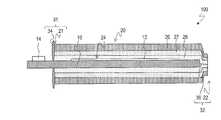
- FIG. 2 is a schematic cross-sectional view of the electronic device 100 taken along the line 2B-2B ′ in FIG. 1.
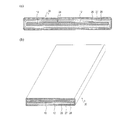
- FIG. 2A is a schematic cross-sectional view of the electronic device 100 taken along line 3B-3B ′ in FIG. 1
- FIG. 2B is a schematic perspective view of the electronic device 100.
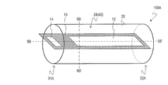
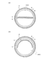
- FIG. 5 is a schematic cross-sectional view of the electronic device 100A along the line 5B-5B ′ in FIG. 4.
- (A) And (b) is typical sectional drawing of the electronic device 100A along the 6B-6B 'line in FIG.
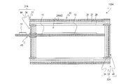
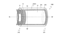
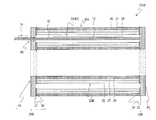
- FIG. 8 is a schematic cross-sectional view of the electronic device 100B taken along line 8B-8B ′ in FIG. 7.
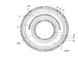
- FIG. 9 is a schematic cross-sectional view of the electronic device 100B taken along line 9B-9B ′ in FIG. 7.
- the electronic device according to the embodiment is a flexible electronic device.
- the present invention is not limited to the embodiments exemplified below.
- components having substantially the same function are denoted by common reference numerals, and description thereof may be omitted.
- FIG. 1 schematically shows an electronic device 100 according to Embodiment 1 of the present invention.
- the electronic device 100 includes a flexible substrate 10, a device unit 12 supported by the flexible substrate 10, a drive circuit unit 14, and a flexible tube 20.
- the water vapor permeability of the flexible tube 20 is less than 10 ⁇ 3 g / (m 2 ⁇ 24 h), and the oxygen permeability is less than 10 ⁇ 2 ml / (m 2 ⁇ 24 h ⁇ MPa).
- the flexible tube 20 forms a first seal structure 31 and a second seal structure 32 at both ends thereof.
- the flexible tube 20 has a sealed space 24 inside thereof. A part of the flexible substrate 10 and the device unit 12 are in the sealed space 24, and the other part of the flexible substrate 10 is outside the sealed space 24.
- the device unit 12 includes a plurality of electronic elements (not shown), and the drive circuit unit 14 includes a circuit that drives the plurality of electronic elements included in the device unit 12.
- the drive circuit unit 14 supplies a predetermined signal to the plurality of organic EL elements.
- the direction of the 2B-2B ′ line in FIG. 1 is the length direction of the flexible tube 20 or the flexible substrate 10
- the direction of the 3B-3B ′ line in FIG. 1 is the width of the flexible tube 20 or the flexible substrate 10.
- direction sometimes called direction.
- the flexible tube 20 Since the flexible tube 20 has low water vapor permeability and oxygen permeability, it is excellent in water vapor barrier properties and oxygen barrier properties.
- the sealed space 24 in the flexible tube 20 is formed by closing both ends of the flexible tube 20 by the first seal structure 31 and the second seal structure 32. Therefore, the electronic device 100 has a seal structure at the end along the width direction of the flexible tube 20, but does not have a seal structure at the end along the length direction of the flexible tube 20.
- the conventional electronic device two resin base materials are bonded together along the length direction and width direction ends of the flexible substrate.
- External moisture and oxygen mainly enter from a bonded portion (seal structure) formed along the lengthwise and widthwise ends of the flexible substrate, causing problems in the electronic device.
- the concentration of moisture and the like is high in the vicinity of the bonded portion, and also increases in the central portion in the sealed space with the passage of time. Therefore, in the conventional electronic device, a defect is likely to occur near the end along the length direction and the end along the width direction.
- the electronic device 100 does not have a seal structure at the end along the length direction of the flexible tube 20, compared to the conventional electronic device, from the end along the length direction of the flexible tube 20, The amount of moisture and oxygen entering the sealed space 24 is reduced. Since the electronic device 100 is in the space 24 in which the device unit 12 is sealed, the influence of moisture and oxygen on the electronic elements of the device unit 12 is reduced. The electronic device 100 is excellent in reliability because the performance of the electronic element is suppressed from decreasing. In particular, when the ratio of the length of the electronic device (flexible tube) to the width (aspect ratio (length / width)) is large, the effect of improving reliability is great. The relationship between the aspect ratio and the reliability of the electronic device (flexible tube) will be described later.
- FIG. 2 and 3 are a schematic sectional view and a perspective view of the electronic device 100.
- FIG. 2 is a schematic cross-sectional view taken along line 2B-2B ′ in FIG. 1
- FIG. 3A is a schematic cross-sectional view taken along line 3B-3B ′ in FIG.
- FIG. 3B is a perspective view.
- the flexible tube 20 of the electronic device 100 includes a tube base material 26, a gas barrier layer 27 inside the tube base material 26, and a seal layer 28 inside the gas barrier layer 27.
- the sealed space 24 of the electronic device 100 has neither gas nor liquid. That is, the inner surface of the flexible tube 20, a part of the flexible substrate 10 in the sealed space 24, and the device unit 12 are in close contact with each other.
- the electronic device according to the embodiment of the present invention is not limited to this.
- the sealed space 24 may be filled with an inert gas or an inert liquid having an insulating property.
- the tube base 26 of the flexible tube 20 includes, for example, polyethylene terephthalate (PET).
- PET polyethylene terephthalate
- the thickness of the tube base material 26 is, for example, 50 ⁇ m.
- the gas barrier layer 27 includes, for example, a metal, an inorganic oxide, or an inorganic nitride.
- the gas barrier layer 27 includes, for example, aluminum (Al), aluminum oxide (alumina: Al 2 O 3 ), silicon dioxide (SiO 2 ), or silicon nitride (SiN x ).
- the gas barrier layer 27 may be a single layer or may have a multilayer structure in which a plurality of layers are stacked.
- the gas barrier layer 27 may have, for example, a structure (SiO 2 / (SiN x / SiO 2 ) n / SiO 2 ) in which silicon dioxide layers and silicon nitride layers are alternately stacked and sandwiched between the silicon dioxide layers.
- the thickness of the gas barrier layer 27 is, for example, 1 ⁇ m to 2 ⁇ m.
- the gas barrier layer 27 is formed on the inside of the tube base material 26 by using, for example, a chemical vapor deposition (CVD) method, a physical vapor deposition (PVD) method, or a sputtering method. .
- CVD chemical vapor deposition
- PVD physical vapor deposition
- sputtering method a method of forming a metal, metal oxide, or ceramic thin film inside the tube.
- a method of forming a metal, metal oxide, or ceramic thin film inside the tube is disclosed in, for example, Japanese Patent No. 4945860.
- the gas barrier layer 27 is formed of an inorganic oxide (for example, alumina)
- the gas barrier layer 27 may be formed using an atomic layer deposition (ALD) method.
- ALD atomic layer deposition
- the gas barrier layer 27 is formed of a material having excellent visible light transmittance, such as aluminum oxide.
- the material of the gas barrier layer 27 can be used regardless of visible light transmittance.
- the gas barrier layer 27 may be formed of aluminum, for example.
- the seal layer 28 is made of, for example, polyethylene (PE).
- the thickness of the seal layer 28 is, for example, 10 ⁇ m.
- the sealing layer 28 may be formed, for example, by bonding a film-like material to the inside of the gas barrier layer 27 with an adhesive.
- the flexible tube 20 may further have a gas adsorption layer (not shown) between the gas barrier layer 27 and the seal layer 28.
- the gas adsorption layer contains, for example, zeolite.
- the thickness of the gas adsorption layer is, for example, 60 ⁇ m.
- a method for forming a zeolite film is disclosed in, for example, Japanese Patent Application Laid-Open No. 2002-249313.
- the flexible tube 20 has both end faces 21 and 22 at both ends in its length direction.
- the flexible tube 20 constitutes the first seal structure 31 or the second seal structure 32 at each of both ends.
- the first seal structure 31 and the second seal structure 32 close both ends of the flexible tube 20, thereby forming a sealed space 24 in the flexible tube 20. That is, the sealed space 24 is defined by the inner surface of the flexible tube 20, the inner surface of the first seal structure 31, and the inner surface of the second seal structure 32.
- the first seal structure 31 includes an end face 21 of the flexible tube 20 and a connection portion 34.
- the end of the flexible tube 20 is closed by a connecting portion 34 that covers the end surface 21 of the flexible tube 20.
- the flexible substrate 10 protrudes from the first seal structure 31.
- the connection part 34 contains resin (for example, epoxy resin or acrylic resin), for example.
- the connection part 34 may be formed from a well-known sealing material used for bonding the substrates of the liquid crystal display device.
- the thickness of the connection part 34 is several micrometers, for example.
- the thickness of the connecting portion 34 may be 5 ⁇ m to 10 ⁇ m, for example.
- the thickness of the connecting portion 34 is the thickness in the normal direction of the end surface 21 of the flexible tube.
- the portion of the surface of the connecting portion 34 that comes into contact with the outside air may be covered with an inorganic oxide (for example, silicon dioxide), an inorganic nitride, or a metal.
- the second seal structure 32 includes an end surface 22 of the flexible tube 20 and a welding surface 36.
- the welding surface 36 is a place where the sealing layers 28 are welded together.
- the sealing layer 28 can be welded using heat and / or pressure.
- the end of the flexible tube 20 is closed by the welding surface 36.
- connection part 34 and / or the welding surface 36 may be called a sealing part.
- the seal structure includes an end face of the flexible tube 20 and a sealing portion.
- the sealing portion is not limited to the connection portion 34 or the welding surface 36 as long as it has a property of closing the end of the flexible tube 20.
- the 1st seal structure 31 has the connection part 34 as a sealing part
- the 2nd seal structure 32 has the welding surface 36 as a sealing part
- a seal structure is not restricted to this.
- the 1st seal structure 31 and the 2nd seal structure 32 may have the connection part 34 and / or the welding surface 36 as a sealing part, respectively.
- the flexible substrate 10 is formed using, for example, polyimide (PI) resin or polyethylene naphthalate (PEN) resin.
- PI polyimide
- PEN polyethylene naphthalate
- the device unit 12 supported by the flexible substrate 10 includes, for example, a plurality of thin film transistors (TFTs) arranged in a matrix having rows and columns.
- the TFT is preferably formed on the flexible substrate 10 at a low temperature.
- the TFT is preferably formed at 300 ° C. or less
- the TFT is preferably formed at 150 ° C. or less.
- a TFT using an oxide semiconductor as an active layer material is preferably used because it is formed at a low temperature.
- the active layer of the TFT included in the device portion 12 includes, for example, an In—Ga—Zn—O-based semiconductor (hereinafter abbreviated as “In—Ga—Zn—O-based semiconductor”).
- a TFT having an In—Ga—Zn—O-based semiconductor layer has high mobility (more than 20 times that of an amorphous silicon (a-Si) TFT) and low leakage current (less than 100 times that of an a-Si TFT). Since it has, it is used suitably as a drive TFT and a pixel TFT. If a TFT having an In—Ga—Zn—O-based semiconductor layer is used, the power consumption of the electronic device can be significantly reduced.
- the In—Ga—Zn—O based semiconductor may be amorphous or may contain a crystalline part.
- a crystalline In—Ga—Zn—O-based semiconductor in which the c-axis is oriented substantially perpendicular to the layer surface is preferable.
- Such a crystal structure of an In—Ga—Zn—O-based semiconductor is disclosed in, for example, Japanese Patent Laid-Open No. 2012-134475. For reference, the entire disclosure of Japanese Patent Application Laid-Open No. 2012-134475 is incorporated herein by reference.
- the active layer of the TFT included in the device portion 12 may include another oxide semiconductor instead of the In—Ga—Zn—O-based semiconductor.
- Zn—O based semiconductor ZnO
- In—Zn—O based semiconductor IZO (registered trademark)
- Zn—Ti—O based semiconductor ZTO
- Cd—Ge—O based semiconductor Cd—Pb—O based
- CdO cadmium oxide
- Mg—Zn—O based semiconductors In—Sn—Zn—O based semiconductors (eg, In 2 O 3 —SnO 2 —ZnO), In—Ga—Sn—O based semiconductors, etc. You may go out.
- the active layer of the TFT included in the device unit 12 may include another semiconductor instead of the oxide semiconductor.
- amorphous silicon, polycrystalline silicon, low-temperature polysilicon (LTPS), or the like may be included.
- the TFT included in the device unit 12 may be an organic TFT (OTFT). Since the organic TFT is formed at a low temperature, it can be suitably used as a TFT formed on the flexible substrate 10.
- OTFT organic TFT
- the device unit 12 further includes an electronic element corresponding to the function of the electronic device 100.
- the electronic device 100 can function as, for example, a display device or a sensor by the electronic element included in the device unit 12.
- the electronic device 100 can function as a display device.
- the electronic device 100 that can function as a display device is not limited to an organic EL display device, and may be various display devices such as an electrophoretic display device, a particle movement display device, and a liquid crystal display device.
- the electronic device 100 that can function as a display device is, for example, an electronic paper (e-Paper), a display panel, or a touch panel combined with a display panel.
- the electronic device 100 can function as a pressure sensor that detects pressure.
- a piezoelectric element is an element that converts a force (pressure) applied to a piezoelectric body into a voltage.
- the piezoelectric body has a property that it deforms when a force (pressure) is applied, and polarization (surface charge) proportional to the force appears.
- the pressure applied to the piezoelectric body is read by the TFT connected to the piezoelectric element by being converted into the surface charge of the piezoelectric body.
- a polymer film having piezoelectricity can be used as the piezoelectric body.
- the piezoelectric polymer film is made of, for example, polyvinylidene fluoride (PVDF) or polylactic acid.
- PVDF polyvinylidene fluoride
- Such an electronic device 100 can also function as a shape measurement sensor that measures position and rotation, for example.
- the electronic device 100 when the device unit 12 includes a piezoelectric element that converts voltage into force (pressure), the electronic device 100 functions as an actuator that utilizes the effect of deforming the piezoelectric body (reverse piezoelectric effect) when voltage is applied. obtain.
- the drive circuit unit 14 is a part that drives an electronic element included in the device unit 12.
- the drive circuit unit 14 includes, for example, a driver IC that supplies a predetermined signal to TFTs (TFT arrays) arranged in a matrix that the device unit 12 has.
- the drive circuit unit 14 includes, for example, a gate driver and a source driver.
- the drive circuit unit 14 of the electronic device 100 is formed on the flexible substrate 10. As shown in FIGS. 1 and 2, the drive circuit unit 14 of the electronic device 100 is outside the sealed space 24.
- the drive circuit unit 14 may be covered with a protective cap (not shown).
- the protective cap that covers the drive circuit unit 14 may be made of a hard material that does not have flexibility.
- the protective cap may be formed of, for example, plastic or metal.
- the electronic device 100 has, for example, a string shape.
- the string shape means that the aspect ratio of the length and width of the electronic device is 10 or more.
- the length of the electronic device is, for example, the length of the flexible substrate in the length direction.
- the length in the length direction of the portion of the flexible substrate covered with the flexible tube may be the length of the electronic device.
- the width of the electronic device is, for example, the length in the width direction of the flexible tube.
- the thickness of the electronic device is, for example, the length in the direction perpendicular to the length direction and the width direction of the flexible tube.
- the length of the electronic device 100 is, for example, 450 mm to 452 mm
- the width of the electronic device 100 is, for example, 5 mm
- the thickness of the electronic device 100 is, for example, 0.2 mm to 0.3 mm.
- the length of the flexible substrate 10 (length in the length direction) is, for example, 450 mm to 452 mm.
- the length of the portion that supports the device portion 12 is, for example, 448 mm
- the length of the portion that supports the drive circuit portion 14 is, for example, 2 mm to 4 mm.
- the width (length in the width direction) of the flexible substrate 10 is, for example, 4.95 mm
- the thickness (length in the length direction and the direction perpendicular to the width direction) is, for example, 30 ⁇ m to 40 ⁇ m.
- the length, width, and thickness of the electronic device according to the embodiment of the present invention are not limited to the above examples.
- the aspect ratio between the length and width of the electronic device according to the embodiment of the present invention may be, for example, 10-50.
- the length of the electronic device according to the embodiment of the present invention is, for example, 50 mm to 1500 mm
- the width of the electronic device according to the embodiment of the present invention is, for example, 5 mm to 30 mm
- the thickness of the electronic device according to the embodiment of the present invention is, for example, 0.05 mm to It may be 0.2 mm.
- the seal structure length is specified.
- the seal structure length is the total distance of the flexible tube or the resin base material bonded together in order to seal the electronic element.
- the location where the flexible tube or resin base material is bonded is inferior to the flexible tube or resin base material itself in terms of water vapor barrier properties and oxygen barrier properties. Therefore, the longer the seal structure length, the more external moisture and oxygen are sealed. The possibility of intruding into the open space increases.
- the seal structure length of the electronic device 100 is 2 of the width of the electronic device 100. Double (2D).
- the seal structure length of a conventional electronic device having the same size is twice (22D) the sum of the length and width of the electronic device. Since the electronic device 100 has a shorter seal structure length than that of the conventional electronic device (0.09 when the conventional electronic device has a seal structure length of 1), moisture that enters the sealed space 24 is present. And / or low oxygen and excellent reliability.
- the seal structure length of the electronic device 100 is 1 / (1 + x), where 1 is the seal structure length of the conventional electronic device.
- the aspect ratio between the length and width of the electronic device 100 is increased, the reliability of the electronic device 100 can be improved more effectively.
- the electronic device 100 is not limited to a string shape.
- the aspect ratio between the length and width of the electronic device 100 may be less than 10.
- the electronic device 100 can be suitably used as a display device, for example.
- the drive circuit unit 14 is formed on the flexible substrate 10, but the electronic device according to the embodiment of the present invention is not limited thereto.
- the drive circuit unit 14 of the electronic device according to the embodiment of the present invention may not be supported by the flexible substrate 10.
- the drive circuit unit 14 of the electronic device according to the embodiment of the present invention may be supported on a substrate (not shown) different from the flexible substrate 10. That is, the drive circuit unit 14 may be provided on a substrate different from the flexible substrate 10, and the substrate may be electrically connected to the flexible substrate 10.
- the electronic device 100 may further include a control circuit unit (not shown).
- the control circuit unit supplies a predetermined signal (including, for example, a start pulse signal, a clock signal, and a digital image signal) to the drive circuit unit 14.
- the control circuit part is outside the sealed space 24, for example.
- the electronic device 100 may further include a plurality of terminals (not shown) connected to the device unit 12 or the drive circuit unit 14.
- the plurality of terminals connected to the device unit 12 or the drive circuit unit 14 may be outside the sealed space 24.
- the drive circuit unit 14 is outside the sealed space 24, but the electronic device according to the embodiment of the present invention is not limited thereto.
- the drive circuit unit 14 of the electronic device according to the embodiment of the present invention may be in the sealed space 24.
- the plurality of terminals connected to the device unit 12 or the drive circuit unit 14 may be outside the sealed space 24 or may be inside the sealed space 24.
- the control circuit unit may also be in the sealed space 24.
- the control circuit unit may have a function of non-contact power reception and / or NFC (Near Field Communication).
- the function of contactless power reception refers to a function of receiving power from a contactless power transmission device using contactless power transmission (wireless power feeding) technology.
- the non-contact power transmission technology is, for example, an electromagnetic induction method or a magnetic resonance method.
- the control circuit unit having a non-contact power receiving function includes, for example, a power receiving electrode.
- a control circuit unit having an NFC (Near Field Communication) function can transmit and receive signals and / or receive power using a short-range wireless communication technology.
- the flexible tube 20 is prepared.
- a flexible tube having an arbitrary length may be prepared and cut to a required length.
- the diameter of the flexible tube is, for example, 3.5 mm.
- the diameter of the flexible tube is, for example, 0.65 to 4 when the width of the flexible substrate 10 is 1.
- the flexible substrate 10 is prepared and the device portion 12 is formed.
- a transfer method can be used to form TFTs on a flexible substrate.
- a TFT array is formed on a polyimide film formed on a glass substrate, and then the polyimide film on which the TFT array is formed is peeled off from the glass substrate and adhered to the flexible substrate.
- the polyimide film is formed, for example, by applying solution-like polyimide (for example, with a thickness of 100 ⁇ m) on a glass substrate and annealing in vacuum.
- the thickness of the polyimide film is, for example, 10 ⁇ m or less.
- a known process can be used for forming the TFT array on the polyimide film on the glass substrate.
- a plurality of TFT arrays used for one electronic device may be formed (multiple chamfering) on the polyimide film. In the case of performing multi-sided cutting, it is transferred to a flexible substrate and then cut into electronic device units.
- a TFT formed at a high temperature can be formed on the flexible substrate 10.
- the process of forming an a-Si TFT reaches 300 ° C. to 350 ° C., but can be formed on the flexible substrate 10 by a transfer method.
- a TFT that can be formed at a low temperature may be formed directly on the flexible substrate 10 without using a transfer method.
- the device part 12 is formed by further forming an electronic element corresponding to the function of the electronic device 100 on the flexible substrate 10.
- a wiring or a terminal connected to the device unit 12 for connecting the device unit 12 and the drive circuit unit 14 may be further formed on the flexible substrate 10.
- the flexible substrate 10 is inserted into the flexible tube 20.
- the flexible substrate 10 protrudes from one end face 21 of the both end faces 21 and 22 of the flexible tube 20.
- the flexible substrate 10 does not protrude from the other end surface 22.
- the flexible substrate 10 is arranged so that the end of the flexible substrate 10 is at a position 0.2 mm inside from the other end surface 22 in the length direction of the flexible tube 20.
- the device unit 12 is inside the flexible tube 20.
- the gas in the flexible tube 20 is vented in an inert gas atmosphere or in a vacuum.
- the inert gas is, for example, nitrogen or a noble gas (for example, argon, helium or neon).
- the flexible tube 20, the part of the flexible substrate 10 in the flexible tube 20, and the device unit 12 are brought into close contact with each other.
- the first seal structure 31 and the second seal structure 32 are formed at both ends of the flexible tube 20 in an inert gas atmosphere or in a vacuum.
- a sealed space 24 is formed in the flexible tube 20.
- the sealed space 24 has neither gas nor liquid.
- a part of the flexible substrate 10 and the device unit 12 are in the sealed space 24, and the remaining part of the flexible substrate 10 is outside the sealed space 24.
- the drive circuit unit 14 is formed outside the sealed space 24.
- the driver IC is connected to a wiring or terminal connected to the device unit 12 on the flexible substrate 10.
- the electronic device 100 is manufactured through the above steps.
- the driving circuit unit 14 may be covered with a protective cap. At this time, necessary wiring is taken out from the protective cap.
- the step of forming the drive circuit unit 14 may be performed before the flexible substrate 10 is inserted into the flexible tube 20.
- the drive circuit unit 14 may be formed integrally with the TFT array (as a driver monolithic type) on the polyimide film or the flexible substrate 10.
- FIG. 4 is a diagram schematically showing the electronic device 100A.
- the direction of line 5B-5B 'in FIG. 4 may be referred to as the length direction of flexible tube 20, and the direction of line 6B-6B' in FIG.
- the electronic device 100A is different from the electronic device 100 in that the sealed space 24 in the flexible tube 20 is filled with an inert gas 42.
- the electronic device 100A may be the same as the electronic device 100 except that the sealed space 24 is filled with an inert gas 42. Since the electronic device 100 ⁇ / b> A does not have a seal structure at the end along the length direction of the flexible tube 20, the entry of external moisture and oxygen into the sealed space 24 is suppressed.
- the electronic device 100A is excellent in reliability because the performance of the electronic element is suppressed from being deteriorated.
- the inert gas 42 is, for example, nitrogen or a rare gas (for example, argon, helium, or neon).
- inert means low reactivity (physically and chemically stable).
- the sealed space 24 of the electronic device 100A may be filled with an inert liquid having an insulating property (for example, liquid perfluorocarbon) instead of the inert gas 42.
- the electronic device 100A has, for example, a cylindrical shape because the sealed space 24 is filled with the inert gas 42. Since the electronic device 100A has a cylindrical shape and good appearance, the electronic device 100A can be suitably used as an electronic device (for example, a display device) used as an interior.
- One side of the flexible substrate 10 of the electronic device 100A is disposed substantially parallel to the length direction of the flexible tube 20, for example, as shown in FIGS.
- the flexible substrate 10 of the electronic device 100 ⁇ / b> A may be arranged in a spiral shape along the inner side of the flexible tube 20.
- the electronic device 100A is excellent in bending resistance.
- 5 and 6 are schematic cross-sectional views of the electronic device 100A.
- 5 is a schematic cross-sectional view taken along the line 5B-5B 'in FIG. 4
- FIG. 6 is a schematic cross-sectional view taken along the line 6B-6B' in FIG.
- the flexible tube 20 constitutes a first seal structure 31A or a second seal structure 32A at each of both ends thereof.
- 1st seal structure 31A contains the end surface 21 of the flexible tube 20, and the connection part 34 and the cover part 44 as a sealing part.
- the lid portion 44 has, for example, the same laminated structure as that of the flexible tube 20.
- the lid portion 44 may be formed from a material different from that of the flexible tube 20.
- the lid portion 44 has, for example, a shape and a size that can cover the end surface 21 of the flexible tube 20.
- the lid portion 44 is a substantially circle having a diameter that is approximately the same length as the diameter of the cylinder.
- the lid 44 has a slit 45 that matches the cross-sectional shape and size of the flexible substrate 10.
- the flexible substrate 10 passes through the slit 45 and protrudes from the first seal structure 31A.
- the connecting portion 34 is provided between the lid portion 44 and the flexible tube 20 and between the slit 45 and the flexible substrate 10.
- the first seal structure 31A may further have a welding surface as a sealing portion.
- the sealing portion of the first seal structure 31A is limited to the connection portion 34 and the lid portion 44 (or the connection portion 34, the lid portion 44 and the welding surface) as long as it has a property of closing the end of the flexible tube 20. Absent.
- the second seal structure 32A includes the end face 22 of the flexible tube 20, and a connection part 34 and a lid part 46 as a sealing part.
- the lid 46 of the second seal structure 32A may be formed from the same material as the lid 44 of the first seal structure 31A, or may be formed from a different material. Since the flexible substrate 10 does not protrude from the second seal structure 32A, the lid 46 of the second seal structure 32A does not have a slit.
- the second seal structure 32A may be the same as the first seal structure 31A except that the lid portion 46 does not have a slit.
- the electronic device 100A can change the shape of the flexible substrate 10 without changing the shape of the electronic device 100A because the sealed space 24 is filled with the inert gas 42.
- the flexible substrate 10 may be a flat surface, or as illustrated in FIG. 6B, the flexible substrate 10 may be a curved surface along the shape of the flexible tube 20. Good.
- the electronic device 100A has, for example, a string shape.
- the electronic device 100A is, for example, a substantially cylinder that extends in the length direction of the flexible tube 20.
- the diameter of the cylindrical electronic device 100A is, for example, 10 mm to 20 mm, and the length of the electronic device 100A is, for example, 450 mm.
- the width of the electronic device 100A is, for example, the diameter of the cylinder.
- the seal structure length of the electronic device 100A is the circumference of the cylinder. 2 times (2 ⁇ D).
- the seal structure length of an electronic device produced by a conventional manufacturing method having the same size is twice the circumference of the cylinder plus two times the length of the electronic device (2 ⁇ D + 20D). Since the electronic device 100A has a shorter seal structure length than an electronic device manufactured by a conventional manufacturing method, it has less moisture and / or oxygen that enter the sealed space 24 and is excellent in reliability.
- the seal structure length of the electronic device 100A is ⁇ / ((1) when the seal structure of the electronic device manufactured by the conventional manufacturing method is 1. ⁇ + x).
- the aspect ratio between the length and width of the electronic device 100A is increased, the reliability of the electronic device 100A can be improved more effectively.
- the electronic device 100A is not limited to a string shape.
- the aspect ratio between the length and the width of the electronic device 100A may be less than 10.
- the cover part 44 and the cover part 46 are prepared.
- the flexible tube 20 for example, a flexible tube having an arbitrary length may be prepared and cut to a required length.
- the diameter of the flexible tube is, for example, 10 mm to 20 mm.
- the diameter of the flexible tube is, for example, the same as the length of the diameter of the electronic device 100A that is a cylinder.
- the lid portion 44 and the lid portion 46 are formed from the same material as the flexible tube 20, the lid portion 44 and the lid portion 46 can be prepared by cutting out from the material of the flexible tube 20.
- the lid portion 44 is provided with a slit 45 that matches the cross section of the flexible substrate 10.
- an adhesive is applied between the flexible tube 20 and the lid portion 44 and between the flexible tube 20 and the lid portion 46 to adhere to each other. The applied adhesive becomes the connection portion 34.
- the flexible substrate 10 is inserted into the flexible tube 20 from the slit 45 of the lid portion 44 of the first seal structure 31A in an inert gas atmosphere or in vacuum.
- the inert gas 42 is filled in the flexible tube 20 in an inert gas atmosphere or in a vacuum.
- FIG. 7 is a diagram schematically showing the electronic device 100B.
- the direction of the 8B-8B ′ line in FIG. 7 is the length direction of the first flexible tube 20A or the second flexible tube 20B
- the direction of the 9B-9B ′ line in FIG. 7 is the first flexible tube 20A or the second flexible tube 20A. It may be referred to as the width direction of the flexible tube 20B.
- the electronic device 100B is different from the electronic device 100A in that the electronic device 100B includes the first flexible tube 20A and the second flexible tube 20B instead of the flexible tube 20.
- the electronic device 100B may be the same as the electronic device 100A except that it has two flexible tubes.
- the water vapor permeability of the first flexible tube 20A is less than 10 ⁇ 3 g / (m 2 ⁇ 24 h), and the oxygen permeability is less than 10 ⁇ 2 ml / (m 2 ⁇ 24 h ⁇ MPa).
- the water vapor permeability of the second flexible tube 20B is less than 10 ⁇ 3 g / (m 2 ⁇ 24 h), and the oxygen permeability is less than 10 ⁇ 2 ml / (m 2 ⁇ 24 h ⁇ MPa).
- the second flexible tube 20B is provided inside the first flexible tube 20A.
- the first flexible tube 20A and the second flexible tube 20B constitute a first seal structure 31B and a second seal structure 32B at both ends.
- the first flexible tube 20A has a sealed space 24 between the second flexible tube 20B.
- the electronic device 100B does not have a seal structure at the ends along the length direction of the first flexible tube 20A and the second flexible tube 20B, external moisture and oxygen may enter the sealed space 24. It is suppressed.
- the electronic device 100B is excellent in reliability because the performance of the electronic element is suppressed from being deteriorated.
- FIG. 8 and 9 are schematic cross-sectional views of the electronic device 100B.
- 8 is a schematic cross-sectional view taken along the line 8B-8B 'in FIG. 7
- FIG. 9 is a schematic cross-sectional view taken along the line 9B-9B' in FIG.
- the first flexible tube 20A may be the same as the flexible tube 20 of the electronic device 100A.
- the second flexible tube 20 ⁇ / b> B has a tube base 26, a gas barrier layer 27 outside the tube base 26, and a seal layer 28 outside the gas barrier layer 27.
- the tube base material 26, the gas barrier layer 27, and the seal layer 28 of the second flexible tube 20B are formed using the same materials and methods as the tube base material 26, the gas barrier layer 27, and the seal layer 28 of the first flexible tube 20A, respectively. obtain.
- the first flexible tube 20A and the second flexible tube 20B have substantially the same length.
- the space between the first flexible tube 20A and the second flexible tube 20B has both end faces 21 and 22 at both ends in the length direction.
- the space between the first flexible tube 20A and the second flexible tube 20B constitutes the first seal structure 31B or the second seal structure 32B at each of both ends.
- a sealed space 24 is formed therebetween. That is, the sealed space 24 is defined by the inner surface of the first flexible tube 20A, the outer surface of the second flexible tube 20B, the inner surface of the first seal structure 31B, and the inner surface of the second seal structure 32B.
- the first seal structure 31B and the second seal structure 32B do not close both ends of the second flexible tube 20B, for example.
- the inside of the second flexible tube 20B is in contact with the outside air.
- the flexible substrate 10 is, for example, a curved surface that follows the shape of the first flexible tube 20A or the second flexible tube 20B.
- the electronic device 100B can be formed into a rod shape by passing, for example, a rod-shaped metal or plastic inside the second flexible tube 20B.
- the shape of the electronic device 100B can be freely changed by passing a foldable wire (for example, a wire) through the inside of the second flexible tube 20B.
- the electronic device 100B has, for example, a string shape.
- the cross section perpendicular to the length direction of the first flexible tube 20A or the second flexible tube 20B of the electronic device 100B includes, for example, a double circle.
- the outer circle of the double circle is a cross section of the first flexible tube 20A
- the inner circle is a cross section of the second flexible tube 20B.
- the width of the electronic device 100B is, for example, the diameter of the outer circle.
- the diameter of the outer circle is, for example, 10 mm to 20 mm.
- the difference between the diameter of the outer circle and the diameter of the inner circle is, for example, 0.4 mm to 1.0 mm.
- the difference between the diameter of the outer circle and the diameter of the inner circle is, for example, 0.01 to 0.2.
- the diameter of the outer circle is 11 mm, for example, and the diameter of the inner circle is 10 mm, for example.
- the length of the electronic device 100B is, for example, 450 mm.
- the seal structure length of the electronic device 100B is , Twice the sum of the circumference of the outer circle and the circumference of the inner circle (2 ⁇ (D + d)).
- the length of the seal structure of an electronic device manufactured by a conventional manufacturing method having the same size is twice the sum of the circumference of the outer circle and the circumference of the inner circle plus four times the length of the electronic device. Length (2 ⁇ (D + d) + 40D). Since the electronic device 100B according to the embodiment of the present invention has a shorter seal structure length than an electronic device manufactured by a conventional manufacturing method, the moisture and / or oxygen that penetrates into the sealed space 24 is less and reliable. Excellent in properties.
- the seal structure length of the electronic device 100B is ( ⁇ (D + d)) where the seal structure length of the electronic device manufactured by the conventional manufacturing method is 1. ) / ( ⁇ (D + d) + 2Dx). Since d is larger than 0 and smaller than D, the seal structure length of the electronic device 100B with respect to the seal structure length of the electronic device manufactured by the conventional manufacturing method is larger than ⁇ / ( ⁇ + 2x) and smaller than ⁇ / ( ⁇ + x). When the aspect ratio between the length and width of the electronic device 100B is increased, the reliability of the electronic device 100B can be more effectively improved.
- the electronic device 100B is not limited to a string shape.
- the aspect ratio between the length and the width of the electronic device 100B may be less than 10.
- the first flexible tube 20A and the second flexible tube 20B are prepared.
- a flexible tube having an arbitrary length may be prepared and cut to a required length.
- the second flexible tube 20B is inserted inside the first flexible tube 20A in an inert atmosphere or in a vacuum.
- the first flexible tube 20A, the second flexible tube 20B, the lid portion 44, and the lid portion 46 are bonded to each other by applying an adhesive.
- the applied adhesive becomes the connection portion 34.
- the subsequent process of manufacturing the electronic device 100B is substantially the same as the manufacturing method of the electronic device 100A.
- the sealed space 24 of the electronic device 100B is filled with the inert gas 42, but the electronic device according to the embodiment of the present invention is not limited thereto.
- the sealed space 24 of the electronic device 100B may have neither gas nor liquid.
- the length of the seal structure of each of the electronic device 100, the electronic device 100A, and the electronic device 100B in which the aspect ratio between the length and the width is x is the seal structure of the electronic device manufactured by the conventional manufacturing method.
- the values are larger than 1 / (1 + x), ⁇ / ( ⁇ + x), and ⁇ / ( ⁇ + 2x) and smaller than ⁇ / ( ⁇ + x), respectively.
- the aspect ratio of the length and the width is the same, the electronic device 100 is most advantageous in that the seal structure length can be shortened as compared with the electronic device manufactured by the conventional manufacturing method, and then the electronic device. 100B is excellent.
- the reliability of the flexible electronic device can be improved.
- the flexible electronic device by embodiment of this invention is used as various electronic devices, such as a flexible display or a flexible sensor, for example.
Landscapes
- Physics & Mathematics (AREA)
- Optics & Photonics (AREA)
- Electromagnetism (AREA)
- Electroluminescent Light Sources (AREA)
Abstract
電子デバイス(100)は、フレキシブル基板(10)と、フレキシブル基板(10)に支持されたデバイス部(12)と、駆動回路部(14)と、水蒸気透過度が10-3g/(m2・24h)未満であり酸素透過度が10-2ml/(m2・24h・MPa)未満であるフレキシブルチューブ(20)とを有し、フレキシブルチューブ(20)は、その両端において第1シール構造(31)および第2シール構造(32)を構成し、その内側に密封された空間(24)を有し、フレキシブル基板(10)の一部分およびデバイス部(12)は、密封された空間(24)の中にあり、フレキシブル基板(10)の一部分以外の部分は、密封された空間(24)の外にある。
Description
本発明は、電子デバイスに関し、特にフレキシブル電子デバイスに関する。
近年、可撓性を有する電子デバイス(フレキシブル電子デバイス)の開発が進められている。有機電子デバイスは、フレキシブル電子デバイスを実用化する電子デバイスの1つとして期待されている。
有機電子デバイスが有する有機エレクトロニクス素子は、水分や酸素に対して敏感なので、水分や酸素の影響によってその性能が劣化することがある。従来は、有機エレクトロニクス素子に対する水分や酸素の影響を軽減するために、例えば、有機エレクトロニクス素子をガラス基板上に配置し、封止缶で覆い、乾燥剤を封入していた。ガラス基板や封止缶は柔軟性を有しないので、このような電子デバイスは、フレキシブル電子デバイスに応用することは困難であった。
特許文献1は、ガスバリア性を有する樹脂基材を開示している。特許文献1の樹脂基材は、樹脂フィルム上に、ガスバリア性に優れた無機酸化物の薄膜を形成したものである。特許文献1は、樹脂基材上に形成され、さらに別の樹脂基材で覆われることにより封止された有機EL素子を開示している。
しかしながら、特許文献1の図8のように、エレクトロニクス素子を覆う2枚の樹脂基材を貼り合わせることにより、エレクトロニクス素子を密封した電子デバイスは、十分な信頼性を得られないことがある。エレクトロニクス素子を密封する2枚の樹脂基材を貼り合わせた箇所は、それぞれの樹脂基材自身に比べて、水蒸気バリア性および酸素バリア性に劣る。このため、樹脂基材を貼り合わせた箇所を透過した水蒸気および酸素に起因して、エレクトロニクス素子の性能が低下し、電子デバイスの信頼性が低下することがある。
本発明は、上記課題を解決するためになされたものであり、水分および/または酸素の影響によってエレクトロニクス素子の性能が低下することを抑制し、フレキシブル電子デバイスの信頼性を向上させることを目的とする。
本発明の実施形態による電子デバイスは、フレキシブル基板と、前記フレキシブル基板に支持されたデバイス部と、駆動回路部と、水蒸気透過度が10-3g/(m2・24h)未満であり酸素透過度が10-2ml/(m2・24h・MPa)未満であるフレキシブルチューブとを有し、前記フレキシブルチューブは、その両端においてシール構造を構成し、その内側に密封された空間を有し、前記フレキシブル基板の一部分および前記デバイス部は、前記密封された空間の中にあり、前記フレキシブル基板の前記一部分以外の部分は、前記密封された空間の外にある。
本発明の他の実施形態による電子デバイスは、フレキシブル基板と、前記フレキシブル基板に支持されたデバイス部と、駆動回路部と、水蒸気透過度が10-3g/(m2・24h)未満であり酸素透過度が10-2ml/(m2・24h・MPa)未満である第1フレキシブルチューブと、前記第1フレキシブルチューブの内側に設けられた、水蒸気透過度が10-3g/(m2・24h)未満であり酸素透過度が10-2ml/(m2・24h・MPa)未満である第2フレキシブルチューブとを有し、前記第1フレキシブルチューブおよび前記第2フレキシブルチューブは、両端においてシール構造を構成し、前記第1フレキシブルチューブは、前記第2フレキシブルチューブとの間に密封された空間を有し、前記フレキシブル基板の一部分および前記デバイス部は、前記密封された空間の中にあり、前記フレキシブル基板の前記一部分以外の部分は、前記密封された空間の外にある。
ある実施形態において、前記密封された空間は、不活性気体または絶縁性を有する不活性液体で満たされている。
ある実施形態において、前記密封された空間は、気体および液体のいずれも有しない。
ある実施形態において、前記駆動回路部は、前記密封された空間の中にある。
ある実施形態において、前記駆動回路部は、前記密封された空間の外にある。
ある実施形態において、前記デバイス部または前記駆動回路部に接続された複数の端子は、前記密封された空間の外にある。
ある実施形態において、前記電子デバイスは、制御回路部をさらに有し、前記制御回路部は、前記密封された空間の中にある。
ある実施形態において、前記制御回路部は、非接触受電またはNFC(Near Field Communication)の機能を含む。
本発明の実施形態によると、水分および/または酸素の影響によってエレクトロニクス素子の性能が低下することを抑制し、フレキシブル電子デバイスの信頼性を向上させることができる。
以下、図面を参照して、本発明の実施形態による電子デバイスを説明する。実施形態による電子デバイスは、フレキシブル電子デバイスである。ただし、本発明は以下で例示する実施形態に限られない。なお、以下の図面において、実質的に同じ機能を有する構成要素は共通の参照符号で示し、その説明を省略することがある。
(実施形態1)
図1に、本発明の実施形態1による電子デバイス100を模式的に示す。
図1に、本発明の実施形態1による電子デバイス100を模式的に示す。
電子デバイス100は、フレキシブル基板10と、フレキシブル基板10に支持されたデバイス部12と、駆動回路部14と、フレキシブルチューブ20とを有する。フレキシブルチューブ20の水蒸気透過度は10-3g/(m2・24h)未満であり、酸素透過度は10-2ml/(m2・24h・MPa)未満である。フレキシブルチューブ20は、その両端において、第1シール構造31および第2シール構造32を構成している。フレキシブルチューブ20は、その内側に、密封された空間24を有する。フレキシブル基板10の一部分とデバイス部12は、密封された空間24の中にあり、フレキシブル基板10のその他の部分は、密封された空間24の外にある。
ここで、デバイス部12は、複数のエレクトロニクス素子(不図示)を含み、駆動回路部14は、デバイス部12が有する複数のエレクトロニクス素子を駆動する回路を含む。例えば、電子デバイス100が有機EL表示装置である場合、デバイス部12は、複数の有機EL素子を含み、駆動回路部14は、複数の有機EL素子に所定の信号を供給する。
なお、以下で、図1中の2B-2B’線の方向をフレキシブルチューブ20またはフレキシブル基板10の長さ方向、図1中の3B-3B’線の方向をフレキシブルチューブ20またはフレキシブル基板10の幅方向ということがある。
フレキシブルチューブ20は、低い水蒸気透過度および酸素透過度を有するので、水蒸気バリア性および酸素バリア性に優れている。フレキシブルチューブ20内の密封された空間24は、第1シール構造31および第2シール構造32によって、フレキシブルチューブ20の両端が閉じられることにより形成されている。従って、電子デバイス100は、フレキシブルチューブ20の幅方向に沿った端にシール構造を有するが、フレキシブルチューブ20の長さ方向に沿った端にシール構造を有しない。
従来の電子デバイスでは、フレキシブル基板の長さ方向および幅方向の端に沿って、2枚の樹脂基材が貼り合わされている。外部の水分および酸素は、フレキシブル基板の長さ方向および幅方向の端に沿って形成された貼り合わせ部(シール構造)から、主に侵入し、エレクトロニクス素子に不具合を発生させる。水分等の濃度は、貼り合わせ部の近傍で高く、時間の経過に伴い密閉された空間内の中央部でも上昇する。したがって、従来の電子デバイスでは、長さ方向に沿った端および幅方向に沿った端の近傍において不具合が発生しやすい。
これに対し、電子デバイス100は、フレキシブルチューブ20の長さ方向に沿った端にシール構造を有しないので、従来の電子デバイスと比較して、フレキシブルチューブ20の長さ方向に沿った端から、密封された空間24内に侵入する水分および酸素の量が低減される。電子デバイス100は、デバイス部12が密封された空間24の中にあるので、デバイス部12が有するエレクトロニクス素子に対する水分および酸素の影響が軽減される。電子デバイス100は、エレクトロニクス素子の性能が低下することが抑制されるので、信頼性に優れている。特に、電子デバイス(フレキシブルチューブ)の長さの幅に対する比(アスペクト比(長さ/幅))が大きい場合に、信頼性の向上効果が大きい。電子デバイス(フレキシブルチューブ)のアスペクト比と信頼性との関係は後述する。
図2および図3に電子デバイス100の模式的な断面図および斜視図を示す。図2は、図1中の2B-2B’線に沿った模式的な断面図であり、図3(a)は、図1中の3B-3B’線に沿った模式的な断面図であり、図3(b)は、斜視図である。
図2および図3に示すように、電子デバイス100のフレキシブルチューブ20は、チューブ基材26と、チューブ基材26の内側にガスバリア層27と、ガスバリア層27の内側にシール層28とを有する。図2および図3に示すように、電子デバイス100の密封された空間24は、気体および液体のいずれも有しない。すなわち、フレキシブルチューブ20の内面と、密封された空間24内にあるフレキシブル基板10の一部分およびデバイス部12とは、密着している。ただし、本発明の実施形態による電子デバイスは、これに限られない。例えば、後述する電子デバイス100A(図4参照)のように、密封された空間24が不活性気体または絶縁性を有する不活性液体で満たされていてもよい。
フレキシブルチューブ20のチューブ基材26は、例えばポリエチレンテレフタレート(PET)を含む。チューブ基材26の厚さは、例えば50μmである。
ガスバリア層27は、例えば、金属、無機酸化物、または無機窒化物を含む。ガスバリア層27は、例えば、アルミニウム(Al)、酸化アルミニウム(アルミナ:Al2O3)、二酸化ケイ素(SiO2)、または窒化ケイ素(SiNx)を含む。ガスバリア層27は、単層であってもよいし、複数の層が積層された多層構造を有していてもよい。ガスバリア層27は、例えば、二酸化ケイ素層と窒化ケイ素層が交互に積層され、二酸化ケイ素層で挟まれた構造(SiO2/(SiNx/SiO2)n/SiO2)であってもよい。ガスバリア層27の厚さは、例えば1μm~2μmである。
ガスバリア層27は、例えば、化学蒸着(Chemical Vapor Deposition:CVD)法、物理蒸着(Physical Vapor Deposition:PVD)法、またはスパッタリング法を用いて、チューブ基材26の内側に成膜されたものである。チューブの内側に金属、金属酸化物、セラミックの薄膜を成膜する方法は、例えば特許第4945860号公報に開示されている。ガスバリア層27が無機酸化物(例えばアルミナ)から形成される場合は、ガスバリア層27は、原子層堆積(Atomic Layer Deposition:ALD)法を用いて成膜されたものであってもよい。
電子デバイス100が表示装置として機能する場合は、ガスバリア層27は、例えば酸化アルミニウム等、可視光の透過性に優れた材料から形成されることが望ましい。電子デバイス100が表示装置として機能しない場合は、ガスバリア層27の材料は、可視光の透過性を問わず用いることができる。電子デバイス100が、例えば、後述するようなセンサーとしてのみ機能する場合は、ガスバリア層27は、例えばアルミニウムから形成されてもよい。
シール層28は、例えばポリエチレン(PE)から形成される。シール層28の厚さは、例えば10μmである。シール層28は、例えば、フィルム状にした材料を、接着材によってガスバリア層27の内側に接着させることにより形成されたものであってもよい。
フレキシブルチューブ20は、ガスバリア層27とシール層28との間に、さらにガス吸着層(不図示)を有していてもよい。ガス吸着層は、例えばゼオライトを含む。ガス吸着層の厚さは、例えば60μmである。ゼオライトの成膜方法は、例えば、特開2002-249313号公報に開示されている。
図2に示すように、フレキシブルチューブ20は、その長さ方向の両端に、両端面21および22を有する。フレキシブルチューブ20は、両端のそれぞれにおいて、第1シール構造31または第2シール構造32を構成する。第1シール構造31および第2シール構造32によって、フレキシブルチューブ20の両端が閉じられることにより、フレキシブルチューブ20内に密封された空間24が形成される。すなわち、密封された空間24は、フレキシブルチューブ20の内面、第1シール構造31の内面、および第2シール構造32の内面によって画定される。
第1シール構造31は、フレキシブルチューブ20の端面21と、接続部34とを含む。第1シール構造31において、フレキシブルチューブ20の端は、フレキシブルチューブ20の端面21を覆う接続部34によって、閉じられる。このとき、フレキシブル基板10は、第1シール構造31から突き出ている。接続部34は、例えば樹脂(例えばエポキシ樹脂またはアクリル樹脂)を含む。接続部34は、液晶表示装置の基板を貼り合わせるために用いられる公知のシール材から形成されてもよい。接続部34の厚さは、例えば数μmである。接続部34の厚さは、例えば5μm~10μmであってもよい。ここで、接続部34の厚さは、フレキシブルチューブの端面21の法線方向における厚さとする。
接続部34の表面のうち、外気と接触する部分は、無機酸化物(例えば二酸化ケイ素)、無機窒化物、または金属で覆われていてもよい。接続部34の表面に無機材料または金属が付与されることで、シール構造を透過する水分および酸素の量が低減される。
第2シール構造32は、フレキシブルチューブ20の端面22と、溶着面36とを含む。溶着面36は、シール層28同士が溶着された箇所である。シール層28の溶着は、熱および/または圧力を用いて行うことができる。第2シール構造32において、フレキシブルチューブ20の端は、溶着面36によって、閉じられる。
接続部34および/または溶着面36を封止部と呼ぶことがある。シール構造は、フレキシブルチューブ20の端面と、封止部とを含む。封止部は、フレキシブルチューブ20の端を閉じる性質を有していれば、接続部34や溶着面36に限られない。ここでは、第1シール構造31は封止部として接続部34を有し、第2シール構造32は封止部として溶着面36を有するが、シール構造はこれに限られない。例えば、第1シール構造31および第2シール構造32は、それぞれ、封止部として接続部34および/または溶着面36を有していてもよい。
再び図1および図2を参照して、電子デバイス100の構造および機能を、詳細に説明する。
フレキシブル基板10は、例えば、ポリイミド(PI)樹脂またはポリエチレンナフタレート(PEN)樹脂を用いて形成される。
フレキシブル基板10に支持されたデバイス部12は、例えば、行および列を有するマトリクス状に配置された複数の薄膜トランジスタ(Thin Film Transistor:TFT)を有する。TFTは、低温で、フレキシブル基板10上に形成されることが好ましい。例えば、フレキシブル基板10がポリイミド樹脂フィルムの場合は300℃以下で、フレキシブル基板10がポリエチレンナフタレート樹脂フィルムの場合は150℃以下で、それぞれ、TFTが形成されることが好ましい。例えば、活性層の材料として酸化物半導体を用いたTFTは、低温で形成されるので、好適に用いられる。
デバイス部12が有するTFTの活性層は、例えばIn-Ga-Zn-O系の半導体(以下、「In-Ga-Zn-O系半導体」と略する。)を含む。ここで、In-Ga-Zn-O系半導体は、In(インジウム)、Ga(ガリウム)、Zn(亜鉛)の三元系酸化物であって、In、GaおよびZnの割合(組成比)は特に限定されず、例えばIn:Ga:Zn=2:2:1、In:Ga:Zn=1:1:1、In:Ga:Zn=1:1:2等を含む。デバイス部12が有するTFTの活性層は、In、Ga、Znを、例えばIn:Ga:Zn=1:1:1の割合で含むIn-Ga-Zn-O系半導体層である。
In-Ga-Zn-O系半導体層を有するTFTは、高い移動度(アモルファスシリコン(a-Si)TFTに比べ20倍超)および低いリーク電流(a-SiTFTに比べ100分の1未満)を有しているので、駆動TFTおよび画素TFTとして好適に用いられる。In-Ga-Zn-O系半導体層を有するTFTを用いれば、電子デバイスの消費電力を大幅に削減することが可能になる。
In-Ga-Zn-O系半導体は、アモルファスでもよいし、結晶質部分を含んでもよい。結晶質In-Ga-Zn-O系半導体としては、c軸が層面に概ね垂直に配向した結晶質In-Ga-Zn-O系半導体が好ましい。このようなIn-Ga-Zn-O系半導体の結晶構造は、例えば、特開2012-134475号公報に開示されている。参考のために、特開2012-134475号公報の開示内容の全てを本明細書に援用する。
デバイス部12が有するTFTの活性層は、In-Ga-Zn-O系半導体の代わりに、他の酸化物半導体を含んでいてもよい。例えばZn-O系半導体(ZnO)、In-Zn-O系半導体(IZO(登録商標))、Zn-Ti-O系半導体(ZTO)、Cd-Ge-O系半導体、Cd-Pb-O系半導体、CdO(酸化カドミウム)、Mg-Zn-O系半導体、In-Sn-Zn-O系半導体(例えばIn2O3-SnO2-ZnO)、In-Ga-Sn-O系半導体などを含んでいてもよい。
デバイス部12が有するTFTの活性層は、酸化物半導体の代わりに、他の半導体を含んでいてもよい。例えばアモルファスシリコン、多結晶シリコン、低温ポリシリコン(LTPS)などを含んでいてもよい。
デバイス部12が有するTFTは、有機TFT(Organic TFT:OTFT)であってもよい。有機TFTは、低温で形成されるので、フレキシブル基板10上に形成されるTFTとして好適に用いられ得る。
デバイス部12は、電子デバイス100の機能に応じたエレクトロニクス素子をさらに有する。デバイス部12が有するエレクトロニクス素子によって、電子デバイス100は、例えば、表示装置またはセンサーとして機能することができる。
例えば、デバイス部12が、複数の有機発光ダイオード(Organic Light-Emitting Diode:OLED)等のEL素子を有するときは、電子デバイス100は、表示装置として機能し得る。表示装置として機能し得る電子デバイス100は、有機EL表示装置に限られず、例えば、電気泳動表示装置や、粒子移動型表示装置、液晶表示装置等、種々の表示装置であってよい。表示装置として機能し得る電子デバイス100は、例えば、電子ペーパー(e-Paper)、表示パネル、または表示パネルと組み合わされたタッチパネルである。
例えば、デバイス部12が、圧電素子(ピエゾ素子)を有するときは、電子デバイス100は、圧力を検知する圧力センサーとして機能し得る。圧電素子は、圧電体に加えられた力(圧力)を電圧に変換する素子である。圧電体は、力(圧力)を加えられると変形し、力に比例した分極(表面電荷)が現れるという性質を有する。圧電体に加えられた圧力は、圧電体の表面電荷に変換されることで、圧電素子に接続されたTFTによって、読み出される。圧電体として、圧電性を有する高分子フィルムを用いることができる。圧電性高分子フィルムは、例えばポリフッ化ビニリデン(PolyVinylidene DiFluoride:PVDF)またはポリ乳酸から形成される。このような電子デバイス100は、例えば、位置および回転を測定する形状測定センサーとしても機能し得る。また、デバイス部12が、電圧を力(圧力)に変換する圧電素子を有するときは、電子デバイス100は、電圧を加えると圧電体が変形する効果(逆圧電効果)を利用したアクチュエータとして機能し得る。
駆動回路部14は、デバイス部12が有するエレクトロニクス素子を駆動する部分である。駆動回路部14は、例えば、デバイス部12が有するマトリクス状に配置されたTFT(TFTアレイ)に所定の信号を供給するドライバICを含む。駆動回路部14は、例えば、ゲートドライバ、ソースドライバを含む。
図1および図2に示すように、電子デバイス100の駆動回路部14は、フレキシブル基板10上に形成されている。図1および図2に示すように、電子デバイス100の駆動回路部14は、密封された空間24の外にある。駆動回路部14は、保護キャップ(不図示)で覆われていてもよい。駆動回路部14を覆う保護キャップは、柔軟性を有しない硬い材質で作られていてもよい。保護キャップは、例えばプラスチック、または金属で形成されていてもよい。駆動回路部14が密封された空間24の外にある場合は、硬い保護キャップで駆動回路部14を覆っても、デバイス部12の柔軟性は損なわれない。
電子デバイス100は、例えば、ひも状である。ここで、ひも状とは、電子デバイスの長さと幅とのアスペクト比が10以上のものをいう。電子デバイスの長さとは、例えば、フレキシブル基板の長さ方向の長さである。フレキシブル基板のうち、フレキシブルチューブに覆われている部分の長さ方向の長さを、電子デバイスの長さとしてもよい。電子デバイスの幅とは、例えば、フレキシブルチューブの幅方向の長さである。電子デバイスの厚さとは、例えば、フレキシブルチューブの長さ方向および幅方向に垂直な方向の長さである。電子デバイス100の長さは例えば450mm~452mm、電子デバイス100の幅は例えば5mm、電子デバイス100の厚さは例えば0.2mm~0.3mmである。フレキシブル基板10の長さ(長さ方向の長さ)は、例えば450mm~452mmである。フレキシブル基板10のうち、デバイス部12を支持する部分の長さが例えば448mm、駆動回路部14を支持する部分の長さが例えば2mm~4mmである。フレキシブル基板10の幅(幅方向の長さ)は例えば4.95mm、フレキシブル基板10の厚さ(長さ方向および幅方向に垂直な方向の長さ)は例えば30μm~40μmである。
ただし、本発明の実施形態による電子デバイスの長さ、幅、および厚さは、上記の例示に限られない。本発明の実施形態による電子デバイスの長さと幅とのアスペクト比は、例えば、10~50であってもよい。本発明の実施形態による電子デバイスの長さは例えば50mm~1500mm、本発明の実施形態による電子デバイスの幅は例えば5mm~30mm、本発明の実施形態による電子デバイスの厚さは例えば0.05mm~0.2mmであってもよい。
ここで、シール構造長を規定する。シール構造長は、エレクトロニクス素子を密封するために、フレキシブルチューブまたは樹脂基材を貼り合わせた総距離の長さである。フレキシブルチューブまたは樹脂基材を貼り合わせた箇所は、フレキシブルチューブまたは樹脂基材自身に比べて、水蒸気バリア性および酸素バリア性に劣るので、シール構造長が長いほど、外部の水分および酸素が密封された空間内に侵入する可能性が大きくなる。
例えば、電子デバイス100の長さと幅とのアスペクト比を10とすると(電子デバイス100の幅をD、長さを10Dとすると)、電子デバイス100のシール構造長は、電子デバイス100の幅の2倍(2D)である。同じサイズを有する従来の電子デバイスのシール構造長は、電子デバイスの長さおよび幅の和の2倍(22D)である。電子デバイス100は、従来の電子デバイスに比べて、シール構造長が短い(従来の電子デバイスのシール構造長を1とすると、0.09である)ので、密封された空間24内に侵入する水分および/または酸素が少なく、信頼性に優れている。電子デバイスの長さと幅とのアスペクト比をxとした場合、電子デバイス100のシール構造長は、従来の電子デバイスのシール構造長を1とすると、1/(1+x)である。電子デバイス100の長さと幅とのアスペクト比を大きくすると、より効果的に、電子デバイス100の信頼性を向上させることができる。
電子デバイス100は、ひも状に限られない。電子デバイス100の長さと幅とのアスペクト比は10未満であってもよい。電子デバイス100の長さと幅とのアスペクト比が10未満である場合、電子デバイス100は、例えば表示装置として好適に用いられ得る。
ここでは、駆動回路部14は、フレキシブル基板10上に形成されているが、本発明の実施形態による電子デバイスはこれに限られない。本発明の実施形態による電子デバイスの駆動回路部14は、フレキシブル基板10に支持されていなくてもよい。本発明の実施形態による電子デバイスの駆動回路部14は、フレキシブル基板10とは異なる基板(不図示)に支持されていてもよい。すなわち、駆動回路部14をフレキシブル基板10とは異なる基板上に設け、この基板をフレキシブル基板10に電気的に接続してもよい。
電子デバイス100は、制御回路部(不図示)をさらに有していてもよい。制御回路部は、例えば、駆動回路部14に所定の信号(例えば、スタートパルス信号、クロック信号、デジタル画像信号を含む)を供給する。制御回路部は、例えば密封された空間24の外にある。
電子デバイス100は、デバイス部12または駆動回路部14に接続された複数の端子(不図示)をさらに有していてもよい。デバイス部12または駆動回路部14に接続された複数の端子は、密封された空間24の外にあってもよい。
ここでは、駆動回路部14は、密封された空間24の外にあるが、本発明の実施形態による電子デバイスはこれに限られない。本発明の実施形態による電子デバイスの駆動回路部14は、密封された空間24の中にあってもよい。このとき、デバイス部12または駆動回路部14に接続された複数の端子は、密封された空間24の外にあってもよいし、密封された空間24の中にあってもよい。デバイス部12または駆動回路部14に接続された複数の端子が密封された空間24の中にあるとき、制御回路部も密封された空間24の中にあってもよい。制御回路部は、非接触受電および/またはNFC(Near Field Communication)の機能を有していてもよい。非接触受電の機能とは、非接触電力伝送(ワイヤレス給電)技術を利用して、非接触送電装置から電力を受ける機能をいう。非接触電力伝送技術は、例えば、電磁誘導方式または磁気共鳴方式である。非接触受電の機能を有する制御回路部は、例えば受電電極を有する。NFC(Near Field Communication)の機能を有する制御回路部は、近距離無線通信技術を利用して、信号を送受信するおよび/または電力を受けることができる。
以下で、電子デバイス100の製造方法を説明する。
まず、フレキシブルチューブ20を用意する。例えば、任意の長さのフレキシブルチューブを用意し、必要な長さにカットしてもよい。フレキシブルチューブの直径は、例えば3.5mmである。フレキシブルチューブの直径は、フレキシブル基板10の幅を1としたとき、例えば、0.65~4である。
次に、フレキシブル基板10を用意し、デバイス部12を形成する。
フレキシブル基板上にTFTを形成するために、例えば、転写法を用いることができる。転写法においては、ガラス基板上に成膜したポリイミド膜の上にTFTアレイを形成し、その後、TFTアレイが形成されたポリイミド膜を、ガラス基板から剥離し、フレキシブル基板上に接着させる。ポリイミド膜は、例えば、ガラス基板上に溶液状のポリイミドを(例えば100μmの厚さで)付与し、真空でアニール処理することにより、形成される。ポリイミド膜の厚さは、例えば10μm以下である。ガラス基板上のポリイミド膜上にTFTアレイを形成するプロセスは、公知のものを用いることができる。ポリイミド膜上に、1つの電子デバイスに用いるTFTアレイを、複数形成(多面取り)してもよい。多面取りを行った場合は、フレキシブル基板上に転写した後で、電子デバイス単位にカットする。
転写法を用いることにより、高温で形成されるTFTであっても、フレキシブル基板10上に形成することができる。例えば、a-SiTFTが形成されるプロセスは300℃~350℃に達するが、転写法によればフレキシブル基板10上に形成することができる。低温で形成することができるTFTは、転写法を用いずに、フレキシブル基板10上に直接形成されてもよい。
フレキシブル基板10上に、電子デバイス100の機能に応じたエレクトロニクス素子をさらに形成することで、デバイス部12を形成する。デバイス部12と駆動回路部14とを接続するための、デバイス部12と接続されている配線または端子を、フレキシブル基板10上にさらに形成してもよい。
次に、フレキシブルチューブ20内に、フレキシブル基板10を挿入する。フレキシブルチューブ20の両端面21および22のうち、一方の端面21からは、フレキシブル基板10が突出する。他方の端面22からは、フレキシブル基板10は突出しない。例えば、フレキシブルチューブ20の長さ方向において、他方の端面22から0.2mm内側の位置にフレキシブル基板10の端があるように、フレキシブル基板10を配置する。このとき、デバイス部12は、フレキシブルチューブ20の内側にある。
次に、不活性気体雰囲気中または真空においてフレキシブルチューブ20内の気体を抜く。不活性気体は、例えば窒素または希ガス(例えばアルゴン、ヘリウムまたはネオン)である。フレキシブルチューブ20と、フレキシブルチューブ20内にあるフレキシブル基板10の一部分およびデバイス部12とを、密着させる。
次に、不活性気体雰囲気中または真空において、フレキシブルチューブ20の両端に、第1シール構造31および第2シール構造32を形成する。第1シール構造31および第2シール構造32によってフレキシブルチューブ20の両端が閉じられることにより、フレキシブルチューブ20内に密封された空間24が形成される。密封された空間24は、気体および液体のいずれも有しない。フレキシブル基板10の一部分とデバイス部12は、密封された空間24の中にあり、フレキシブル基板10の残りの部分は、密封された空間24の外にある。
次に、密封された空間24の外に駆動回路部14を形成する。例えば、フレキシブル基板10上のデバイス部12と接続されている配線または端子に、ドライバICを接続する。
以上の工程により、電子デバイス100が製造される。駆動回路部14に、保護キャップをかぶせてもよい。このとき、必要な配線は、保護キャップから取り出す。駆動回路部14を形成する工程は、フレキシブルチューブ20内にフレキシブル基板10を挿入する前に行ってもよい。駆動回路部14は、ポリイミド膜上またはフレキシブル基板10上にTFTアレイと一体として(ドライバモノリシック型として)形成されてもよい。
次に、図4を参照して、本実施形態の他の電子デバイス100Aの構造を説明する。図4は、電子デバイス100Aを模式的に示した図である。図4中の5B-5B’線の方向を、フレキシブルチューブ20の長さ方向、図4中の6B-6B’線の方向を、フレキシブルチューブ20の幅方向ということがある。
電子デバイス100Aは、フレキシブルチューブ20内の密封された空間24が不活性気体42で満たされている点において、電子デバイス100と異なる。電子デバイス100Aは、密封された空間24が不活性気体42で満たされている点を除いて、電子デバイス100と同じであってよい。電子デバイス100Aは、フレキシブルチューブ20の長さ方向に沿った端にシール構造を有しないので、密封された空間24内に、外部の水分および酸素が侵入することが抑制される。電子デバイス100Aは、エレクトロニクス素子の性能が低下することが抑制されるので、信頼性に優れている。
不活性気体42は、例えば、窒素または希ガス(例えばアルゴン、ヘリウムまたはネオン)である。ここで不活性とは、反応性が低い(物理的および化学的に安定である)ことをいう。電子デバイス100Aの密封された空間24は、不活性気体42の代わりに、絶縁性を有する不活性な液体(例えば液体状のパーフルオロカーボン)で満たされていてもよい。電子デバイス100Aは、密封された空間24に不活性気体42が充填されているので、例えば円筒形状を有する。電子デバイス100Aは、円筒形状であり見栄えがよいので、インテリアとして用いられる電子デバイス(例えば表示装置)として好適に用いられ得る。
電子デバイス100Aのフレキシブル基板10の一辺は、例えば、図4および図5に示すように、フレキシブルチューブ20の長さ方向とほぼ平行に配置されている。これに限られず、電子デバイス100Aのフレキシブル基板10は、フレキシブルチューブ20の内側に沿った螺旋状に配置されていてもよい。フレキシブル基板10が螺旋状に配置されている場合は、電子デバイス100Aは、曲げ耐性に優れている。
図5および図6に電子デバイス100Aの模式的な断面図を示す。図5は、図4中の5B-5B’線に沿った模式的な断面図であり、図6は、図4中の6B-6B’線に沿った模式的な断面図である。
図5に示すように、フレキシブルチューブ20は、その両端のそれぞれにおいて、第1シール構造31Aまたは第2シール構造32Aを構成する。
第1シール構造31Aは、フレキシブルチューブ20の端面21と、封止部として接続部34および蓋部44とを含む。蓋部44は、図5に示すように、例えば、フレキシブルチューブ20と同じ積層構造を有する。蓋部44は、フレキシブルチューブ20とは異なる材料から形成されていてもよい。蓋部44は、例えば、フレキシブルチューブ20の端面21を覆うことができる形状およびサイズを有する。例えば、電子デバイス100Aが円筒形である場合、蓋部44は、円筒の直径とほぼ同じ長さの直径を有するほぼ円である。蓋部44は、フレキシブル基板10の断面の形状およびサイズに合わせたスリット45を有する。フレキシブル基板10は、スリット45内を通り、第1シール構造31Aから突き出ている。接続部34は、例えば、蓋部44とフレキシブルチューブ20との間およびスリット45とフレキシブル基板10との間に設けられる。
蓋部44がフレキシブルチューブ20と同じ材料から形成されている場合は、蓋部44およびフレキシブルチューブ20のシール層28同士を、溶着することができる。この場合、第1シール構造31Aは、封止部として、溶着面をさらに有していてもよい。第1シール構造31Aの封止部は、フレキシブルチューブ20の端を閉じる性質を有していれば、接続部34および蓋部44(または、接続部34、蓋部44および溶着面)に限られない。
第2シール構造32Aは、フレキシブルチューブ20の端面22と、封止部として接続部34および蓋部46とを含む。第2シール構造32Aの蓋部46は、第1シール構造31Aの蓋部44と同じ材料から形成されていてもよいし、異なる材料から形成されていてもよい。フレキシブル基板10は第2シール構造32Aから突き出ないので、第2シール構造32Aの蓋部46はスリットを有しない。第2シール構造32Aは、蓋部46がスリットを有しない点を除いて、第1シール構造31Aと同じであってよい。
図6に示すように、電子デバイス100Aは、密封された空間24に不活性気体42が充填されていることにより、電子デバイス100Aの形状を変えることなく、フレキシブル基板10の形状を変えることができる。例えば、図6(a)に示すように、フレキシブル基板10は平面であってもよいし、図6(b)に示すように、フレキシブル基板10はフレキシブルチューブ20の形状に沿う曲面であってもよい。
電子デバイス100Aは、例えば、ひも状である。電子デバイス100Aは、例えば、フレキシブルチューブ20の長さ方向に伸びる、ほぼ円筒である。円筒である電子デバイス100Aの直径は、例えば10mm~20mm、電子デバイス100Aの長さは、例えば450mmである。電子デバイス100Aが円筒であるとき、電子デバイス100Aの幅は、例えば円筒の直径である。
例えば、円筒である電子デバイス100Aの長さと幅とのアスペクト比を10とすると(電子デバイス100Aの幅をD、長さを10Dとすると)、電子デバイス100Aのシール構造長は、円筒の円周の2倍(2πD)である。同じサイズを有する従来の製造方法で作製された電子デバイスのシール構造長は、円筒の円周の2倍に、電子デバイスの長さの2倍を加えたもの(2πD+20D)である。電子デバイス100Aは、従来の製造方法で作製された電子デバイスに比べて、シール構造長が短いので、密封された空間24内に侵入する水分および/または酸素が少なく、信頼性に優れている。
円筒である電子デバイス100Aの長さと幅とのアスペクト比をxとした場合、電子デバイス100Aのシール構造長は、従来の製造方法で作製された電子デバイスのシール構造を1とすると、π/(π+x)である。電子デバイス100Aの長さと幅とのアスペクト比を大きくすると、より効果的に、電子デバイス100Aの信頼性を向上させることができる。
電子デバイス100Aは、ひも状に限られない。電子デバイス100Aの長さと幅とのアスペクト比は10未満であってもよい。
以下で、電子デバイス100Aの製造方法について説明する。電子デバイス100の製造方法と同じ工程については、説明を省略する。
まず、フレキシブルチューブ20を用意するとともに、蓋部44および蓋部46を用意する。フレキシブルチューブ20は、例えば任意の長さのフレキシブルチューブを用意し、必要な長さにカットしてもよい。フレキシブルチューブの直径は、例えば10mm~20mmである。フレキシブルチューブの直径は、例えば、円筒である電子デバイス100Aの直径の長さと同じである。
蓋部44および蓋部46を、フレキシブルチューブ20と同じ材料から形成する場合は、フレキシブルチューブ20の材料から切り取ることにより、蓋部44および蓋部46を用意することができる。蓋部44には、フレキシブル基板10の断面に合わせたスリット45を設ける。不活性気体雰囲気中または真空において、フレキシブルチューブ20と蓋部44との間およびフレキシブルチューブ20と蓋部46との間に、それぞれ、接着材を付与し、互いに接着させる。付与された接着材が接続部34となる。
フレキシブル基板10を用意し、デバイス部12を形成した後、不活性気体雰囲気中または真空において、フレキシブルチューブ20内に、第1シール構造31Aの蓋部44のスリット45からフレキシブル基板10を挿入する。不活性気体雰囲気中または真空において、フレキシブルチューブ20内に不活性気体42を充填する。第1シール構造31Aにおけるスリット45とフレキシブル基板10との間に接着材を付与することによりこれらを接着させ、密封された空間24を形成する。付与された接着材が接続部34となる。
(実施形態2)
次に、図7を参照して、本発明の実施形態2による電子デバイス100Bの構造を説明する。図7は、電子デバイス100Bを模式的に示した図である。図7中の8B-8B’線の方向を、第1フレキシブルチューブ20Aまたは第2フレキシブルチューブ20Bの長さ方向、図7中の9B-9B’線の方向を、第1フレキシブルチューブ20Aまたは第2フレキシブルチューブ20Bの幅方向ということがある。
次に、図7を参照して、本発明の実施形態2による電子デバイス100Bの構造を説明する。図7は、電子デバイス100Bを模式的に示した図である。図7中の8B-8B’線の方向を、第1フレキシブルチューブ20Aまたは第2フレキシブルチューブ20Bの長さ方向、図7中の9B-9B’線の方向を、第1フレキシブルチューブ20Aまたは第2フレキシブルチューブ20Bの幅方向ということがある。
電子デバイス100Bは、フレキシブルチューブ20に代えて、第1フレキシブルチューブ20Aおよび第2フレキシブルチューブ20Bを有する点において、電子デバイス100Aと異なる。電子デバイス100Bは、フレキシブルチューブを2つ有する点を除いて、電子デバイス100Aと同じであってよい。
第1フレキシブルチューブ20Aの水蒸気透過度は10-3g/(m2・24h)未満であり、酸素透過度は10-2ml/(m2・24h・MPa)未満である。第2フレキシブルチューブ20Bの水蒸気透過度が10-3g/(m2・24h)未満であり、酸素透過度は10-2ml/(m2・24h・MPa)未満である。第2フレキシブルチューブ20Bは、第1フレキシブルチューブ20Aの内側に設けられている。第1フレキシブルチューブ20Aおよび第2フレキシブルチューブ20Bは、両端において第1シール構造31Bおよび第2シール構造32Bを構成している。第1フレキシブルチューブ20Aは、第2フレキシブルチューブ20Bとの間に、密封された空間24を有する。
電子デバイス100Bは、第1フレキシブルチューブ20Aおよび第2フレキシブルチューブ20Bの長さ方向に沿った端にシール構造を有しないので、密封された空間24内に、外部の水分および酸素が侵入することが抑制される。電子デバイス100Bは、エレクトロニクス素子の性能が低下することが抑制されるので、信頼性に優れている。
図8および図9に電子デバイス100Bの模式的な断面図を示す。図8は、図7中の8B-8B’線に沿った模式的な断面図であり、図9は、図7中の9B-9B’線に沿った模式的な断面図である。
図8および図9に示すように、第1フレキシブルチューブ20Aは、電子デバイス100Aのフレキシブルチューブ20と同じであってよい。第2フレキシブルチューブ20Bは、チューブ基材26と、チューブ基材26の外側にガスバリア層27と、ガスバリア層27の外側にシール層28とを有する。第2フレキシブルチューブ20Bのチューブ基材26、ガスバリア層27およびシール層28は、それぞれ、第1フレキシブルチューブ20Aのチューブ基材26、ガスバリア層27およびシール層28と同じ材料および方法を用いて形成され得る。
図8に示すように、第1フレキシブルチューブ20Aおよび第2フレキシブルチューブ20Bは、ほぼ同じ長さを有する。図8に示すように、第1フレキシブルチューブ20Aと第2フレキシブルチューブ20Bとの間の空間は、長さ方向の両端に、両端面21および22を有する。第1フレキシブルチューブ20Aと第2フレキシブルチューブ20Bとの間の空間は、両端のそれぞれにおいて、第1シール構造31Bまたは第2シール構造32Bを構成する。第1シール構造31Bおよび第2シール構造32Bによって、第1フレキシブルチューブ20Aと第2フレキシブルチューブ20Bとの間の空間の両端が閉じられることにより、第1フレキシブルチューブ20Aと第2フレキシブルチューブ20Bとの間に密封された空間24が形成される。すなわち、密封された空間24は、第1フレキシブルチューブ20Aの内面、第2フレキシブルチューブ20Bの外面、第1シール構造31Bの内面、および第2シール構造32Bの内面によって画定される。
第1シール構造31Bおよび第2シール構造32Bは、例えば、第2フレキシブルチューブ20Bの両端を閉じるものではない。この場合、第2フレキシブルチューブ20Bの内側は外気に接する。
図9に示すように、フレキシブル基板10は、例えば、第1フレキシブルチューブ20Aまたは第2フレキシブルチューブ20Bの形状に沿う曲面である。図9に示すように、電子デバイス100Bは、第2フレキシブルチューブ20Bの内側に例えば棒状の金属またはプラスチックを通すことで、棒状とすることができる。第2フレキシブルチューブ20Bの内側に、折り曲げることができるもの(例えば針金)を通すことで、電子デバイス100Bの形状を自在に変えることができる。
電子デバイス100Bは、例えば、ひも状である。電子デバイス100Bの、第1フレキシブルチューブ20Aまたは第2フレキシブルチューブ20Bの長さ方向に垂直な断面は、例えば、二重円を含む。二重円の外側の円は第1フレキシブルチューブ20Aの断面であり、内側の円は第2フレキシブルチューブ20Bの断面である。電子デバイス100Bの幅は、例えば、外側の円の直径である。外側の円の直径は、例えば10mm~20mmである。外側の円の直径と、内側の円の直径との差は、例えば0.4mm~1.0mmである。外側の円の直径を1とすると、外側の円の直径と、内側の円の直径との差は、例えば0.01~0.2である。外側の円の直径は例えば11mmであり、内側の円の直径は例えば10mmである。電子デバイス100Bの長さは、例えば450mmである。
例えば、電子デバイス100Bの長さと幅とのアスペクト比を10とすると(電子デバイス100Bの幅をD、長さを10D、内側の円の直径をdとすると)、電子デバイス100Bのシール構造長は、外側の円の円周および内側の円の円周の和の2倍(2π(D+d))である。同じサイズを有する従来の製造方法で作製された電子デバイスのシール構造長は、外側の円の円周および内側の円の円周の和の2倍に、電子デバイスの長さの4倍を加えた長さ(2π(D+d)+40D)である。本発明の実施形態による電子デバイス100Bは、従来の製造方法で作製された電子デバイスに比べて、シール構造長が短いので、密封された空間24内に侵入する水分および/または酸素が少なく、信頼性に優れている。
電子デバイス100Bの長さと幅とのアスペクト比をxとした場合、電子デバイス100Bのシール構造長は、従来の製造方法で作製された電子デバイスのシール構造長を1とすると、(π(D+d))/(π(D+d)+2Dx)である。dは0より大きくDより小さいので、従来の製造方法で作製された電子デバイスのシール構造長に対する電子デバイス100Bのシール構造長は、π/(π+2x)より大きくπ/(π+x)より小さい。電子デバイス100Bの長さと幅とのアスペクト比を大きくすると、より効果的に、電子デバイス100Bの信頼性を向上させることができる。
電子デバイス100Bは、ひも状に限られない。電子デバイス100Bの長さと幅とのアスペクト比は10未満であってもよい。
以下で、電子デバイス100Bの製造方法について説明する。電子デバイス100Aの製造方法と同じ工程については、説明を省略する。
最初に、第1フレキシブルチューブ20Aおよび第2フレキシブルチューブ20Bを用意する。例えば、それぞれ、任意の長さのフレキシブルチューブを用意し、必要な長さにカットしてもよい。
次に、不活性雰囲気中または真空において、第1フレキシブルチューブ20Aの内側に、第2フレキシブルチューブ20Bを挿入する。不活性気体雰囲気中または真空において、第1フレキシブルチューブ20A、第2フレキシブルチューブ20B、蓋部44および蓋部46を、接着材を付与することにより、互いに接着させる。付与された接着材が接続部34となる。
これに続く、電子デバイス100Bを製造する工程は、電子デバイス100Aの製造方法と実質的に同じである。
電子デバイス100Bの密封された空間24は不活性気体42で満たされているが、本発明の実施形態による電子デバイスはこれに限られない。電子デバイス100Bの密封された空間24は、気体および液体のいずれも有しなくてもよい。
上述したように、いずれも長さと幅とのアスペクト比がxである、電子デバイス100、電子デバイス100A、および電子デバイス100Bのシール構造長は、従来の製造方法で作製された電子デバイスのシール構造長を1とすると、それぞれ、1/(1+x)、π/(π+x)、およびπ/(π+2x)より大きくπ/(π+x)より小さい値である。長さと幅とのアスペクト比が同じである場合、従来の製造方法で作製された電子デバイスと比較して、シール構造長を短くできる点において、電子デバイス100が最も有利であり、次に電子デバイス100Bが優れている。
本発明の実施形態によると、フレキシブル電子デバイスの信頼性を向上させることができる。本発明の実施形態によるフレキシブル電子デバイスは、例えば、フレキシブルディスプレイ、またはフレキシブルセンサー等、種々の電子デバイスとして用いられる。
10 フレキシブル基板
12 デバイス部
14 駆動回路部
20 フレキシブルチューブ
20A 第1フレキシブルチューブ
20B 第2フレキシブルチューブ
21、22 端面
24 密封された空間
26 チューブ基材
27 ガスバリア層
28 シール層
31、31A、31B 第1シール構造
32、32A、32B 第2シール構造
34 接続部
36 溶着面
42 不活性気体
44、46 蓋部
45 スリット
100、100A、100B 電子デバイス
12 デバイス部
14 駆動回路部
20 フレキシブルチューブ
20A 第1フレキシブルチューブ
20B 第2フレキシブルチューブ
21、22 端面
24 密封された空間
26 チューブ基材
27 ガスバリア層
28 シール層
31、31A、31B 第1シール構造
32、32A、32B 第2シール構造
34 接続部
36 溶着面
42 不活性気体
44、46 蓋部
45 スリット
100、100A、100B 電子デバイス
Claims (9)
- フレキシブル基板と、前記フレキシブル基板に支持されたデバイス部と、駆動回路部と、
水蒸気透過度が10-3g/(m2・24h)未満であり酸素透過度が10-2ml/(m2・24h・MPa)未満であるフレキシブルチューブとを有し、
前記フレキシブルチューブは、その両端においてシール構造を構成し、その内側に密封された空間を有し、
前記フレキシブル基板の一部分および前記デバイス部は、前記密封された空間の中にあり、
前記フレキシブル基板の前記一部分以外の部分は、前記密封された空間の外にある、電子デバイス。 - フレキシブル基板と、前記フレキシブル基板に支持されたデバイス部と、駆動回路部と、
水蒸気透過度が10-3g/(m2・24h)未満であり酸素透過度が10-2ml/(m2・24h・MPa)未満である第1フレキシブルチューブと、
前記第1フレキシブルチューブの内側に設けられた、水蒸気透過度が10-3g/(m2・24h)未満であり酸素透過度が10-2ml/(m2・24h・MPa)未満である第2フレキシブルチューブとを有し、
前記第1フレキシブルチューブおよび前記第2フレキシブルチューブは、両端においてシール構造を構成し、
前記第1フレキシブルチューブは、前記第2フレキシブルチューブとの間に密封された空間を有し、
前記フレキシブル基板の一部分および前記デバイス部は、前記密封された空間の中にあり、
前記フレキシブル基板の前記一部分以外の部分は、前記密封された空間の外にある、電子デバイス。 - 前記密封された空間は、不活性気体または絶縁性を有する不活性液体で満たされている、請求項1または2に記載の電子デバイス。
- 前記密封された空間は、気体および液体のいずれも有しない、請求項1または2に記載の電子デバイス。
- 前記駆動回路部は、前記密封された空間の中にある、請求項1から4のいずれかに記載の電子デバイス。
- 前記駆動回路部は、前記密封された空間の外にある、請求項1から4のいずれかに記載の電子デバイス。
- 前記デバイス部または前記駆動回路部に接続された複数の端子は、前記密封された空間の外にある、請求項1から6のいずれかに記載の電子デバイス。
- 制御回路部をさらに有し、
前記制御回路部は、前記密封された空間の中にある、請求項1から5のいずれかに記載の電子デバイス。 - 前記制御回路部は、非接触受電またはNFC(Near Field Communication)の機能を含む、請求項8に記載の電子デバイス。
Priority Applications (1)
| Application Number | Priority Date | Filing Date | Title |
|---|---|---|---|
| US15/129,045 US10193101B2 (en) | 2014-03-26 | 2015-03-24 | Electronic device |
Applications Claiming Priority (2)
| Application Number | Priority Date | Filing Date | Title |
|---|---|---|---|
| JP2014063435 | 2014-03-26 | ||
| JP2014-063435 | 2014-03-26 |
Publications (1)
| Publication Number | Publication Date |
|---|---|
| WO2015146975A1 true WO2015146975A1 (ja) | 2015-10-01 |
Family
ID=54195487
Family Applications (1)
| Application Number | Title | Priority Date | Filing Date |
|---|---|---|---|
| PCT/JP2015/058904 Ceased WO2015146975A1 (ja) | 2014-03-26 | 2015-03-24 | 電子デバイス |
Country Status (2)
| Country | Link |
|---|---|
| US (1) | US10193101B2 (ja) |
| WO (1) | WO2015146975A1 (ja) |
Families Citing this family (3)
| Publication number | Priority date | Publication date | Assignee | Title |
|---|---|---|---|---|
| CN107924244B (zh) * | 2015-09-15 | 2021-06-15 | 株式会社村田制作所 | 操作检测装置 |
| CN111312027A (zh) * | 2018-12-11 | 2020-06-19 | 北京纳米能源与系统研究所 | 基于聚乳酸压电薄膜的微型马达、驱动器和盲文显示器 |
| DE102020200053A1 (de) * | 2020-01-06 | 2021-07-08 | Heliatek Gmbh | Verkapselungssystem für ein optoelektronisches Bauelement mit mindestens einer ersten Verkapselung und einer zweiten Verkapselung, optoelektronisches Bauelement mit einem solchen Verkapselungssystem |
Citations (6)
| Publication number | Priority date | Publication date | Assignee | Title |
|---|---|---|---|---|
| JPH05283162A (ja) * | 1992-03-31 | 1993-10-29 | Iwasaki Electric Co Ltd | エレクトロルミネッセンス素子 |
| JP2001118674A (ja) * | 1999-10-19 | 2001-04-27 | Auto Network Gijutsu Kenkyusho:Kk | 有機el表示装置 |
| JP2008293680A (ja) * | 2007-05-22 | 2008-12-04 | Konica Minolta Holdings Inc | 有機エレクトロルミネッセンス素子及びその製造方法 |
| JP2011509645A (ja) * | 2007-12-20 | 2011-03-24 | ゼネラル・エレクトリック・カンパニイ | 非接触電力およびデータ伝送システムならびに方法 |
| JP2011108564A (ja) * | 2009-11-20 | 2011-06-02 | Seiko Epson Corp | 電気光学装置、電気光学装置の製造方法ならびに電子機器 |
| WO2013094407A1 (ja) * | 2011-12-21 | 2013-06-27 | 日東電工株式会社 | トップエミッション型の有機エレクトロルミネッセンス素子の製造方法 |
Family Cites Families (13)
| Publication number | Priority date | Publication date | Assignee | Title |
|---|---|---|---|---|
| JP2002249313A (ja) | 2000-12-19 | 2002-09-06 | Toray Ind Inc | ゼオライト結晶のコーティング方法、ゼオライト結晶がコーティングされた基材、ゼオライト膜の製造方法、ゼオライト膜、および分離方法 |
| JP4945860B2 (ja) | 2001-07-24 | 2012-06-06 | 凸版印刷株式会社 | バリア性チューブ状容器 |
| JP2006299145A (ja) | 2005-04-22 | 2006-11-02 | Konica Minolta Holdings Inc | ガスバリア性フィルム、ガスバリア性フィルムを用いた有機エレクトロルミネッセンス用樹脂基材および有機エレクトロルミネッセンス素子 |
| WO2007144995A1 (ja) * | 2006-06-15 | 2007-12-21 | Sharp Kabushiki Kaisha | 表示装置及びその製造方法 |
| KR100824902B1 (ko) * | 2006-12-13 | 2008-04-23 | 삼성에스디아이 주식회사 | 유기 전계 발광 표시 장치 및 그 제조 방법 |
| WO2009072226A1 (ja) * | 2007-12-06 | 2009-06-11 | Sharp Kabushiki Kaisha | 可撓性を有する表示装置 |
| DE102008062130A1 (de) * | 2008-12-16 | 2010-06-17 | Tesa Se | Verfahren zur Kapselung einer elektronischen Anordnung |
| WO2011155117A1 (ja) * | 2010-06-09 | 2011-12-15 | シャープ株式会社 | 表示装置 |
| WO2012002272A1 (ja) * | 2010-06-29 | 2012-01-05 | シャープ株式会社 | 可撓性表示装置および可撓性表示装置の製造方法 |
| CN103339715B (zh) | 2010-12-03 | 2016-01-13 | 株式会社半导体能源研究所 | 氧化物半导体膜以及半导体装置 |
| KR102079188B1 (ko) * | 2012-05-09 | 2020-02-19 | 가부시키가이샤 한도오따이 에네루기 켄큐쇼 | 발광 장치 및 전자 기기 |
| KR102167315B1 (ko) * | 2014-04-30 | 2020-10-20 | 삼성디스플레이 주식회사 | 유기전계발광 표시장치 |
| WO2016033703A1 (zh) * | 2014-09-02 | 2016-03-10 | 深圳市柔宇科技有限公司 | 显示模组及具有该显示模组的电子装置 |
-
2015
- 2015-03-24 WO PCT/JP2015/058904 patent/WO2015146975A1/ja not_active Ceased
- 2015-03-24 US US15/129,045 patent/US10193101B2/en active Active
Patent Citations (6)
| Publication number | Priority date | Publication date | Assignee | Title |
|---|---|---|---|---|
| JPH05283162A (ja) * | 1992-03-31 | 1993-10-29 | Iwasaki Electric Co Ltd | エレクトロルミネッセンス素子 |
| JP2001118674A (ja) * | 1999-10-19 | 2001-04-27 | Auto Network Gijutsu Kenkyusho:Kk | 有機el表示装置 |
| JP2008293680A (ja) * | 2007-05-22 | 2008-12-04 | Konica Minolta Holdings Inc | 有機エレクトロルミネッセンス素子及びその製造方法 |
| JP2011509645A (ja) * | 2007-12-20 | 2011-03-24 | ゼネラル・エレクトリック・カンパニイ | 非接触電力およびデータ伝送システムならびに方法 |
| JP2011108564A (ja) * | 2009-11-20 | 2011-06-02 | Seiko Epson Corp | 電気光学装置、電気光学装置の製造方法ならびに電子機器 |
| WO2013094407A1 (ja) * | 2011-12-21 | 2013-06-27 | 日東電工株式会社 | トップエミッション型の有機エレクトロルミネッセンス素子の製造方法 |
Also Published As
| Publication number | Publication date |
|---|---|
| US20170110680A1 (en) | 2017-04-20 |
| US10193101B2 (en) | 2019-01-29 |
Similar Documents
| Publication | Publication Date | Title |
|---|---|---|
| US11107840B2 (en) | Method for fabricating a semiconductor device comprising an oxide semiconductor | |
| US9623633B2 (en) | Flexible display and method for manufacturing the same | |
| US8436342B2 (en) | Organic light emitting display device and method of manufacturing the same | |
| He et al. | Oxide-based thin film transistors for flexible electronics | |
| US9461269B2 (en) | Organic light emitting display and method of fabricating the same | |
| US9806285B2 (en) | Organic light-emitting diode display and manufacturing method thereof | |
| US10217958B2 (en) | Method of manufacturing curved display device | |
| JP2022171652A (ja) | 表示装置 | |
| JP2024105377A (ja) | 半導体装置 | |
| US9184224B2 (en) | Organic light-emitting diode display and manufacturing method thereof | |
| US20160104867A1 (en) | Organic light emitting diode display panel and method of fabricating the same | |
| CN101800288A (zh) | 光传感器、光传感器装置和显示装置 | |
| US10877599B2 (en) | Touch sensing unit and display device including the same | |
| WO2015146975A1 (ja) | 電子デバイス | |
| US20220102560A1 (en) | Thin-film transistor substrate and method of manufacturing thin-film transistor substrate | |
| CN116072734A (zh) | 薄膜晶体管以及包括薄膜晶体管的显示装置 | |
| JP6717596B2 (ja) | 半導体装置 | |
| JP2010016072A (ja) | 薄膜トランジスタ | |
| KR20250127052A (ko) | 반도체 장치 및 전자 기기 | |
| JP4214152B2 (ja) | 表示装置 | |
| CN115810670A (zh) | 薄膜晶体管、其制造方法以及包括其的显示装置 | |
| US20260090220A1 (en) | Thin film transistor substrate and display device comprising the same | |
| WO2015114870A1 (ja) | ガスセンサ | |
| KR102949188B1 (ko) | 박막 트랜지스터 및 이를 포함하는 표시장치 | |
| US20260026236A1 (en) | Display Device |
Legal Events
| Date | Code | Title | Description |
|---|---|---|---|
| 121 | Ep: the epo has been informed by wipo that ep was designated in this application |
Ref document number: 15768667 Country of ref document: EP Kind code of ref document: A1 |
|
| NENP | Non-entry into the national phase |
Ref country code: DE |
|
| WWE | Wipo information: entry into national phase |
Ref document number: 15129045 Country of ref document: US |
|
| NENP | Non-entry into the national phase |
Ref country code: JP |
|
| 122 | Ep: pct application non-entry in european phase |
Ref document number: 15768667 Country of ref document: EP Kind code of ref document: A1 |