WO2015146016A1 - 反射防止機能付きレンズの製造方法 - Google Patents
反射防止機能付きレンズの製造方法 Download PDFInfo
- Publication number
- WO2015146016A1 WO2015146016A1 PCT/JP2015/001253 JP2015001253W WO2015146016A1 WO 2015146016 A1 WO2015146016 A1 WO 2015146016A1 JP 2015001253 W JP2015001253 W JP 2015001253W WO 2015146016 A1 WO2015146016 A1 WO 2015146016A1
- Authority
- WO
- WIPO (PCT)
- Prior art keywords
- film
- lens
- dielectric multilayer
- multilayer film
- warm water
- Prior art date
- Legal status (The legal status is an assumption and is not a legal conclusion. Google has not performed a legal analysis and makes no representation as to the accuracy of the status listed.)
- Ceased
Links
Images


Classifications
-
- B—PERFORMING OPERATIONS; TRANSPORTING
- B32—LAYERED PRODUCTS
- B32B—LAYERED PRODUCTS, i.e. PRODUCTS BUILT-UP OF STRATA OF FLAT OR NON-FLAT, e.g. CELLULAR OR HONEYCOMB, FORM
- B32B9/00—Layered products comprising a layer of a particular substance not covered by groups B32B11/00 - B32B29/00
-
- C—CHEMISTRY; METALLURGY
- C03—GLASS; MINERAL OR SLAG WOOL
- C03C—CHEMICAL COMPOSITION OF GLASSES, GLAZES OR VITREOUS ENAMELS; SURFACE TREATMENT OF GLASS; SURFACE TREATMENT OF FIBRES OR FILAMENTS MADE FROM GLASS, MINERALS OR SLAGS; JOINING GLASS TO GLASS OR OTHER MATERIALS
- C03C17/00—Surface treatment of glass, not in the form of fibres or filaments, by coating
- C03C17/34—Surface treatment of glass, not in the form of fibres or filaments, by coating with at least two coatings having different compositions
- C03C17/3411—Surface treatment of glass, not in the form of fibres or filaments, by coating with at least two coatings having different compositions with at least two coatings of inorganic materials
-
- B—PERFORMING OPERATIONS; TRANSPORTING
- B32—LAYERED PRODUCTS
- B32B—LAYERED PRODUCTS, i.e. PRODUCTS BUILT-UP OF STRATA OF FLAT OR NON-FLAT, e.g. CELLULAR OR HONEYCOMB, FORM
- B32B15/00—Layered products comprising a layer of metal
- B32B15/20—Layered products comprising a layer of metal comprising aluminium or copper
-
- B—PERFORMING OPERATIONS; TRANSPORTING
- B32—LAYERED PRODUCTS
- B32B—LAYERED PRODUCTS, i.e. PRODUCTS BUILT-UP OF STRATA OF FLAT OR NON-FLAT, e.g. CELLULAR OR HONEYCOMB, FORM
- B32B5/00—Layered products characterised by the non- homogeneity or physical structure, i.e. comprising a fibrous, filamentary, particulate or foam layer; Layered products characterised by having a layer differing constitutionally or physically in different parts
- B32B5/14—Layered products characterised by the non- homogeneity or physical structure, i.e. comprising a fibrous, filamentary, particulate or foam layer; Layered products characterised by having a layer differing constitutionally or physically in different parts characterised by a layer differing constitutionally or physically in different parts, e.g. denser near its faces
- B32B5/147—Layered products characterised by the non- homogeneity or physical structure, i.e. comprising a fibrous, filamentary, particulate or foam layer; Layered products characterised by having a layer differing constitutionally or physically in different parts characterised by a layer differing constitutionally or physically in different parts, e.g. denser near its faces by treatment of the layer
-
- C—CHEMISTRY; METALLURGY
- C03—GLASS; MINERAL OR SLAG WOOL
- C03C—CHEMICAL COMPOSITION OF GLASSES, GLAZES OR VITREOUS ENAMELS; SURFACE TREATMENT OF GLASS; SURFACE TREATMENT OF FIBRES OR FILAMENTS MADE FROM GLASS, MINERALS OR SLAGS; JOINING GLASS TO GLASS OR OTHER MATERIALS
- C03C17/00—Surface treatment of glass, not in the form of fibres or filaments, by coating
- C03C17/22—Surface treatment of glass, not in the form of fibres or filaments, by coating with other inorganic material
- C03C17/23—Oxides
- C03C17/245—Oxides by deposition from the vapour phase
-
- C—CHEMISTRY; METALLURGY
- C03—GLASS; MINERAL OR SLAG WOOL
- C03C—CHEMICAL COMPOSITION OF GLASSES, GLAZES OR VITREOUS ENAMELS; SURFACE TREATMENT OF GLASS; SURFACE TREATMENT OF FIBRES OR FILAMENTS MADE FROM GLASS, MINERALS OR SLAGS; JOINING GLASS TO GLASS OR OTHER MATERIALS
- C03C17/00—Surface treatment of glass, not in the form of fibres or filaments, by coating
- C03C17/34—Surface treatment of glass, not in the form of fibres or filaments, by coating with at least two coatings having different compositions
- C03C17/3411—Surface treatment of glass, not in the form of fibres or filaments, by coating with at least two coatings having different compositions with at least two coatings of inorganic materials
- C03C17/3429—Surface treatment of glass, not in the form of fibres or filaments, by coating with at least two coatings having different compositions with at least two coatings of inorganic materials at least one of the coatings being a non-oxide coating
- C03C17/3447—Surface treatment of glass, not in the form of fibres or filaments, by coating with at least two coatings having different compositions with at least two coatings of inorganic materials at least one of the coatings being a non-oxide coating comprising a halide
- C03C17/3452—Surface treatment of glass, not in the form of fibres or filaments, by coating with at least two coatings having different compositions with at least two coatings of inorganic materials at least one of the coatings being a non-oxide coating comprising a halide comprising a fluoride
-
- G—PHYSICS
- G02—OPTICS
- G02B—OPTICAL ELEMENTS, SYSTEMS OR APPARATUS
- G02B1/00—Optical elements characterised by the material of which they are made; Optical coatings for optical elements
- G02B1/10—Optical coatings produced by application to, or surface treatment of, optical elements
- G02B1/11—Anti-reflection coatings
- G02B1/113—Anti-reflection coatings using inorganic layer materials only
- G02B1/115—Multilayers
-
- G—PHYSICS
- G02—OPTICS
- G02B—OPTICAL ELEMENTS, SYSTEMS OR APPARATUS
- G02B1/00—Optical elements characterised by the material of which they are made; Optical coatings for optical elements
- G02B1/10—Optical coatings produced by application to, or surface treatment of, optical elements
- G02B1/11—Anti-reflection coatings
- G02B1/118—Anti-reflection coatings having sub-optical wavelength surface structures designed to provide an enhanced transmittance, e.g. moth-eye structures
-
- B—PERFORMING OPERATIONS; TRANSPORTING
- B32—LAYERED PRODUCTS
- B32B—LAYERED PRODUCTS, i.e. PRODUCTS BUILT-UP OF STRATA OF FLAT OR NON-FLAT, e.g. CELLULAR OR HONEYCOMB, FORM
- B32B2551/00—Optical elements
-
- C—CHEMISTRY; METALLURGY
- C03—GLASS; MINERAL OR SLAG WOOL
- C03C—CHEMICAL COMPOSITION OF GLASSES, GLAZES OR VITREOUS ENAMELS; SURFACE TREATMENT OF GLASS; SURFACE TREATMENT OF FIBRES OR FILAMENTS MADE FROM GLASS, MINERALS OR SLAGS; JOINING GLASS TO GLASS OR OTHER MATERIALS
- C03C2217/00—Coatings on glass
- C03C2217/20—Materials for coating a single layer on glass
- C03C2217/21—Oxides
- C03C2217/214—Al2O3
-
- C—CHEMISTRY; METALLURGY
- C03—GLASS; MINERAL OR SLAG WOOL
- C03C—CHEMICAL COMPOSITION OF GLASSES, GLAZES OR VITREOUS ENAMELS; SURFACE TREATMENT OF GLASS; SURFACE TREATMENT OF FIBRES OR FILAMENTS MADE FROM GLASS, MINERALS OR SLAGS; JOINING GLASS TO GLASS OR OTHER MATERIALS
- C03C2217/00—Coatings on glass
- C03C2217/20—Materials for coating a single layer on glass
- C03C2217/21—Oxides
- C03C2217/22—ZrO2
-
- C—CHEMISTRY; METALLURGY
- C03—GLASS; MINERAL OR SLAG WOOL
- C03C—CHEMICAL COMPOSITION OF GLASSES, GLAZES OR VITREOUS ENAMELS; SURFACE TREATMENT OF GLASS; SURFACE TREATMENT OF FIBRES OR FILAMENTS MADE FROM GLASS, MINERALS OR SLAGS; JOINING GLASS TO GLASS OR OTHER MATERIALS
- C03C2217/00—Coatings on glass
- C03C2217/70—Properties of coatings
- C03C2217/73—Anti-reflective coatings with specific characteristics
- C03C2217/734—Anti-reflective coatings with specific characteristics comprising an alternation of high and low refractive indexes
-
- C—CHEMISTRY; METALLURGY
- C03—GLASS; MINERAL OR SLAG WOOL
- C03C—CHEMICAL COMPOSITION OF GLASSES, GLAZES OR VITREOUS ENAMELS; SURFACE TREATMENT OF GLASS; SURFACE TREATMENT OF FIBRES OR FILAMENTS MADE FROM GLASS, MINERALS OR SLAGS; JOINING GLASS TO GLASS OR OTHER MATERIALS
- C03C2218/00—Methods for coating glass
- C03C2218/10—Deposition methods
- C03C2218/15—Deposition methods from the vapour phase
- C03C2218/154—Deposition methods from the vapour phase by sputtering
Definitions
- the present invention relates to a method for producing an antireflective lens, and more particularly to a method for producing a nonreflective coating comprising a dielectric multilayer film on one side and a structured nonreflective coating on the other side. .
- an antireflective film having a concavo-convex structure has a wide band and can suppress the reflectance to a low level for light rays from low to high angles, but has a problem that it is weak against rubbing because of the concavo-convex shape. is there.
- Patent Document 2 discloses a lens in which a dielectric multilayer film is formed on one surface and a concavo-convex structure film of boehmite is formed on the other surface.
- a dielectric film is formed on one surface of a lens, then alumina is formed on the other surface, and then the film is immersed in warm water to form a fine uneven structure film. It is done.
- Patent Document 3 discloses a method of forming an alumina film on the other side in a non-coated (untreated) state on one side, and then performing warm water treatment to form a fine uneven structure film.
- patent document 3 does not describe the process after formation of a fine uneven structure film, if a dielectric multilayer film is formed on one side after forming the fine uneven structure film, the dielectric multilayer film is formed on one side. It is possible to obtain a lens in which an antireflective film comprising the above is formed, and an antireflective film comprising the fine uneven structure film on the other surface.
- the present invention has been made in view of the above-mentioned circumstances, and manufactures a lens with an anti-reflection function with high yield with a multi-layer dielectric film on one surface and an anti-reflection coating on the other surface. To provide a manufacturing method.
- a dielectric multilayer film is formed on one surface of a lens body, and a film containing aluminum is formed on the other surface of the lens body,
- a method of manufacturing a lens with an antireflection function by converting a film containing aluminum into a fine uneven structure film containing alumina hydrate as a main component by immersing only the surface on which a film containing aluminum is formed in warm water. is there.
- the period (average pitch) of the unevenness of the fine uneven structure film is made sufficiently smaller than the wavelength of light to be used.
- the outermost surface of the dielectric multilayer film can be made of a layer made of MgF 2 .
- the immersion time in hot water can be 1 minute or more.
- an anti-reflection film made of a dielectric multilayer film is formed on one surface of the lens body, an anti-reflection film made of a fine uneven structure film is formed on the other surface. Since it is formed, the handling property is high, the risk of defects occurring in the fine concavo-convex structure film is reduced, and it is possible to manufacture with high yield.
- the fine uneven structure film when forming the fine uneven structure film, only the surface on which the film containing aluminum is formed is immersed in the warm water, without immersing the dielectric multilayer film previously formed in warm water.
- the dielectric multilayer film is not affected by the warm water treatment, and good antireflective film performance can be maintained without causing spectral characteristics even in the warm water treatment process.
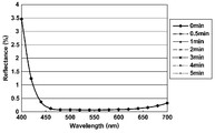
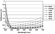
- FIG. 1 It is a cross-sectional schematic diagram which shows the lens manufactured by the manufacturing method of embodiment of this invention. It is a perspective view explaining the manufacturing method of the embodiment of the present invention. It is a figure which shows the cross section of FIG. It is a figure which shows the wavelength dependency of the reflectance of the dielectric multilayer of a lens manufactured by carrying out warm water processing by different processing time in the manufacturing method of an Example. It is a figure which shows the wavelength dependency of the reflectance of the dielectric multilayer of a lens manufactured by carrying out warm water process by different processing time in the manufacturing method of a comparative example, and manufacturing it.
- FIG. 1 is a schematic cross-sectional view of a lens 1 with an anti-reflection function manufactured by the method for manufacturing an anti-reflection lens according to an embodiment of the present invention.
- the lens 1 with an anti-reflection film is provided with an antireflection film consisting of a lens body 2 and a dielectric multilayer film 3 provided on one surface 2a, and the other surface 2b. It comprises the anti-reflective film which consists of the fine concavo-convex structure film 4.
- the lens body 2 is prepared, the dielectric multilayer film 3 is formed on one surface 2 a of the lens body 2, and a film containing aluminum is formed on the other surface 2 b. Only the surface 2b on which the film containing aluminum is formed is immersed in warm water (boiling water) to change the film containing aluminum into a fine uneven structure film containing alumina hydrate as a main component, thereby reflecting on both surfaces 2a and 2b It is a method of manufacturing a lens with anti-reflection provided with a protective film.
- a film containing aluminum an aluminum film, an alumina film, etc. may be mentioned, and any film which is boehmite by hot water treatment and changes to a fine uneven structure film containing alumina hydrate as a main component may be used.
- the immersion of the surface 2 b in warm water is performed by holding the lens body 2 so that the dielectric multilayer film 3 formed on the one surface 2 a is not immersed in water.
- the immersion time in warm water is preferably 1 minute or more.
- FIG. 2 is a perspective view for explaining a lens main body holding state at the time of hot water treatment
- FIG. 3 is a cross-sectional view for explaining a liquid level and a water immersion area of the lens.
- FIGS. 2 and 3 show an example in which a large number of lenses are treated simultaneously with the hot water treatment instead of a single lens, the same applies to the case where a single lens is subjected to hot water treatment.
- the lens 12 has a dielectric multilayer film 13 formed on one surface 12 a and a film 14 a containing aluminum formed on the other surface 12 b.
- the lens holder 31 capable of simultaneously holding 12 is set so that the surface on which the film 14a containing aluminum is formed is on the liquid surface side (lower surface).
- the lens holder 31 is horizontally held by the hanging tool 30 at its four corners, and only one side 12b of the lens 12 is in contact with the liquid surface.
- the film 14a containing aluminum changes to a transparent fine uneven structure film containing alumina hydrate as a main component.
- the hanging tool 30 shown in FIG. 2 is composed of four threads, and the threads are inserted into the holes provided at the four corners of the lens holder 31 and tied and fixed, and the lengths of the four threads are adjusted. It is configured to be held horizontally.
- the configuration of the lens holder at the time of hot water treatment consisting of the lens holder 31 and the hanging tool 30 is particularly limited as long as it can hold only one side of the lens so as to be submerged in the hot water treatment.
- the end portion of the lens body may be held and held.
- Hydrates of alumina are boehmite (denoted as Al 2 O 3 ⁇ H 2 O or AlOOH) which is alumina monohydrate, and bayerite (Al) which is alumina trihydrate (aluminum hydroxide). 2 O 3 ⁇ 3 H 2 O or Al (OH) 3 ).
- the period (average pitch) of the unevenness of the fine uneven structure film 4 is sufficiently smaller than the wavelength of light (for example, visible light and infrared light) to be used. Specifically, the period of the fine unevenness is on the order of several tens of nm to several hundreds of nm.
- the pitch is the distance between the apexes of the nearest adjacent projections separated by the depressions, and the depth is the distance from the apex of the projections to the bottom of the adjacent depressions.
- the fine concavo-convex structure film has a structure that becomes more sparse as it gets away from the base material (the width of the void corresponding to the recess becomes larger and the width of the protrusion becomes smaller), and the refractive index becomes smaller as it gets away from the base Become.
- the average pitch of the asperities can be determined by, for example, photographing a surface image of the fine asperity structure with an SEM (scanning electron microscope), performing image processing to binarize the image, and performing statistical processing.
- the film thickness of the uneven structure film can be obtained by photographing a cross-sectional image of the fine uneven structure film and processing the image.
- the dielectric multilayer film 3 formed on one surface 2a is generally formed by alternately laminating low refractive index layers and high refractive index layers.
- MgF 2 , SiO 2 , Al 2 O 3 can be used as the low refractive index layer, and TiO 2 , ZrO 2 , Ta 2 O 5 , Nb 2 O 5 or the like can be used as the high refractive index layer.
- the outermost surface of the dielectric multilayer film 3 is preferably a layer made of MgF 2 .
- the hot water treatment for forming the fine uneven structure film is performed without immersing the dielectric multilayer film 3 in water, the spectral characteristics of the dielectric multilayer film 3 are not changed. Good antireflective film performance of the dielectric multilayer film 3 can be maintained.
- the layer composed of MgF 2 has low water resistance, and the change in spectral characteristics due to the hot water treatment is very large. Especially when the warm water treatment time is 1 minute or more, the change is remarkable. Therefore, when the dielectric multi-layered film having the layer of MgF 2 as the outermost surface is provided, the manufacturing method of the present invention has remarkable effects.
- the handling property is high, the risk of defects occurring in the fine uneven structure film can be reduced, and manufacturing can be performed with high yield.
- Example The manufacturing method of the lens with an anti-reflection function of the Example was performed in the following procedure.
- the lens body 2 was formed by polishing or molding from a lens glass material (BK7), and an antireflective film made of a dielectric multilayer film was formed on one surface 2a of the lens body 2.
- BK7 lens glass material
- 81 nm of Al 2 O 3 , 131 nm of ZrO 2, and 98 nm of MgF 2 were formed in this order on the lens surface 2 a by vapor deposition.
- Al 2 O 3 was deposited to a thickness of 80 nm by sputtering on the other surface 2 b of the lens body 2.
- a fixed time in boiling water (Example 1: 0.5 minutes, Example 2: 1 minutes, Example 3: 2 minutes, Example 4: 3 minutes, Example 5: 4 minutes, Example 6: 5 minutes)
- the lens was pulled up and cooled, and then immersed in IPA (isopropyl alcohol) and dried.
- IPA isopropyl alcohol
- the anti-reflection function of the dielectric multilayer film was measured for the lenses of each of Examples 1 to 6 treated by changing the warm water treatment time.
- a spectrum was measured with a reflection spectrometer (FE3000 manufactured by Otsuka Electronics Co., Ltd.).
- FIG. 4 shows the result, and is a graph showing the wavelength dependency of the reflectance in each example. Regardless of the time of the warm water treatment, the result that the reflectance of the dielectric multilayer film of the lens of any of the examples shows the same wavelength dependency was obtained. Since the dielectric multilayer film was not immersed in warm water, it is considered that there was no change in the characteristics.
- the lens body 2 was formed by polishing or molding from a lens glass material (BK7), and an antireflective film made of a dielectric multilayer film was formed on one surface 2a of the lens body 2.
- BK7 lens glass material
- 81 nm of Al 2 O 3 , 131 nm of ZrO 2, and 98 nm of MgF 2 were formed in this order on the lens surface 2 a by vapor deposition.
- FIG. 5 shows the results and is a graph showing the wavelength dependency of the reflectance in each example.
- the wavelength dependency of the reflectance of the dielectric multilayer film of the lens changed significantly, and the reflectance increased significantly after the hot water treatment.
- the reflectance increase after processing was larger as the increase rate of the reflectance was larger in one minute or more, and the processing time was longer. This is a result showing that the reflection characteristic of the dielectric multilayer film is changed by simultaneously treating the dielectric multilayer film with warm water.
Landscapes
- Chemical & Material Sciences (AREA)
- Physics & Mathematics (AREA)
- Geochemistry & Mineralogy (AREA)
- Life Sciences & Earth Sciences (AREA)
- Engineering & Computer Science (AREA)
- Chemical Kinetics & Catalysis (AREA)
- General Chemical & Material Sciences (AREA)
- Materials Engineering (AREA)
- Organic Chemistry (AREA)
- General Physics & Mathematics (AREA)
- Optics & Photonics (AREA)
- Inorganic Chemistry (AREA)
- Surface Treatment Of Optical Elements (AREA)
- Laminated Bodies (AREA)
- Surface Treatment Of Glass (AREA)
Abstract
【課題】反射防止機能付きレンズを歩留まり良く製造する。 【解決手段】レンズ本体(12)の一方の面(12a)に誘電体多層膜(3)を形成し、レンズ本体(12)の他方の面(12b)にアルミニウムを含む膜(14a)を形成し、アルミニウムを含む膜(14a)を温水に浸漬させることにより、アルミニウムを含む膜(14a)をアルミナ水和物を主成分とする微細凹凸構造膜に変化させることにより、両面(12a、12b)に反射防止機能を備えたレンズを製造する。
Description
本発明は、反射防止機能付きレンズの製造方法に関し、特には一方の面に誘電体多層膜からなる無反射コーティング、他方の面に構造化無反射コーティングを施したレンズの製造方法に関するものである。
従来、ガラス、プラスチックなどの透光性媒質を用いた光学素子(レンズ)には、表面反射が多いとフレアーやゴーストが多く発生し、また透過率が低下するので表面に薄膜の誘電体膜よりなる反射防止膜が施されている。この反射防止膜には、光学素子に入射する光束の入射角度範囲が広くても、良好なる反射防止効果が得られることが要望されている。広い入射角度範囲で高い反射防止効果を得るには、空気と層との間や、層と層との間の界面を構成する膜の屈折率差が小さいことが必要である。これを実現する方法として、可視光の波長以下の微細凹凸を表面に形成することにより反射防止機能を付与する構造化無反射コーティングが知られている(特許文献1など)。
一方で、凹凸構造を持つ反射防止膜は広帯域であり低~高角度からの光線に対して反射率を低く抑えることが可能であるが凹凸の形状であるがゆえに擦りに対して弱いという問題がある。
特許文献2には、一方の面に誘電体多層膜、他方の面にベーマイトによる凹凸構造膜が形成されたレンズが開示されている。特許文献2の実施例2ではレンズの一方の面に誘電体膜を形成後、他方の面にアルミナを成膜し、その後温水中に浸漬することにより微細凹凸構造膜を形成する製造方法が採用されている。
特許文献3には、一方の面はノンコート(未処理)の状態で、他方の面にアルミナを成膜し、その後温水処理を行い微細凹凸構造膜を形成する方法が開示されている。特許文献3には微細凹凸構造膜形成後の処理について記載されていないが、微細凹凸構造膜を形成後に、一方の面に誘電体多層膜を成膜すれば、一方の面に誘電体多層膜からなる反射防止膜、他方の面に微細凹凸構造膜からなる反射防止膜が形成されてなるレンズを得ることができる。
特許文献3には、一方の面はノンコート(未処理)の状態で、他方の面にアルミナを成膜し、その後温水処理を行い微細凹凸構造膜を形成する方法が開示されている。特許文献3には微細凹凸構造膜形成後の処理について記載されていないが、微細凹凸構造膜を形成後に、一方の面に誘電体多層膜を成膜すれば、一方の面に誘電体多層膜からなる反射防止膜、他方の面に微細凹凸構造膜からなる反射防止膜が形成されてなるレンズを得ることができる。
特許文献2のように、一方の面に誘電体多層膜を形成後、他方の面にアルミニウムを形成して温水処理を行うと、誘電体多層膜によっては、分光特性が変化してしまうという問題が生じることが本発明者らの検討により明らかになった。
特許文献3のように、先に他方の面に温水処理を伴う微細凹凸構造膜の形成を行い、その後、一方の面に誘電体多層膜を形成すれば、上記問題は生じない。しかしながら、微細凹凸構造膜は破損し易いものであるため、誘電体多層膜の成膜処理工程時に微細凹凸構造膜に器具、ヒトの手等が触れることにより凹凸構造膜の剥がれ、欠陥等が生じて部分的に分光特性が劣化し、不良品となってしまう危険性が高く、結果的に製造歩留まりが低下してしまう。
本願発明は、上記事情に鑑みてなされたものであって、一方の面に誘電体多層膜、他方の面に微細凹凸構造膜からなる反射防止コートを備えた反射防止機能付きレンズを歩留まり良く製造する製造方法を提供することを目的とする。
本発明の反射防止機能付きレンズの製造方法は、レンズ本体の一方の面に誘電体多層膜を形成し、レンズ本体の他方の面にアルミニウムを含む膜を形成し、
アルミニウムを含む膜が形成された面のみを温水に浸漬させることにより、アルミニウム含む膜をアルミナ水和物を主成分とする微細凹凸構造膜に変換させて反射防止機能付きのレンズを製造する方法である。
アルミニウムを含む膜が形成された面のみを温水に浸漬させることにより、アルミニウム含む膜をアルミナ水和物を主成分とする微細凹凸構造膜に変換させて反射防止機能付きのレンズを製造する方法である。
微細凹凸構造膜の凹凸の周期(平均ピッチ)は使用される光の波長よりも十分に小さいものとする。
誘電体多層膜の最表面をMgF2からなる層とすることができる。
温水に浸漬する時間は、1分以上とすることができる。
本発明の反射防止機能付きレンズの製造方法によれば、レンズ本体の一方の面に誘電体多層膜からなる反射防止膜を形成した後に、他方の面に微細凹凸構造膜からなる反射防止膜を形成するので、ハンドリング性が高く、微細凹凸構造膜に欠陥が生じるリスクを低減し、歩留まり良く製造することが可能である。
また、微細凹凸構造膜を形成する際に、先に形成されている誘電体多層膜を温水中に浸漬させることなく、アルミニウムを含む膜が形成されている面のみを温水中に浸漬させるので、誘電体多層膜は温水処理の影響を受けず、温水処理工程においても分光特性をさせることなく良好な反射防止膜性能を維持することができる。
以下、図面を参照して本発明の実施の形態を説明する。
図1は、本発明の実施形態に係る反射防止機能付きレンズの製造方法により製造される反射防止機能付きレンズ1の断面模式図である。
図1に示すように、無反射防止膜付きレンズ1は、レンズ本体2と、その一方の面2aに設けられた誘電体多層膜3からなる反射防止膜と、他方の面2bに設けられた微細凹凸構造膜4からなる反射防止膜とから構成される。
図1に示すように、無反射防止膜付きレンズ1は、レンズ本体2と、その一方の面2aに設けられた誘電体多層膜3からなる反射防止膜と、他方の面2bに設けられた微細凹凸構造膜4からなる反射防止膜とから構成される。
反射防止機能付きレンズの製造方法は、レンズ本体2を用意し、レンズ本体2の一方の面2aに誘電体多層膜3を形成し、他方の面2bにアルミニウムを含む膜を形成し、その後、アルミニウムを含む膜が形成された面2bのみを温水(沸騰水)に浸漬させてアルミニウムを含む膜をアルミナ水和物を主成分とする微細凹凸構造膜に変化させることにより両面2a、2bに反射防止膜を備えた反射防止付きレンズを製造する方法である。
アルミニウムを含む膜としては、アルミニウム膜、アルミナ膜などが挙げられ、温水処理によりベーマイト化されてアルミナ水和物を主成分とする微細凹凸構造膜に変化するものであればよい。
面2bの温水への浸漬は、一方の面2aに形成された誘電体多層膜3が水に浸らないようにレンズ本体2を保持して行う。温水への浸漬時間は1分以上とすることが好ましい。
図2は温水処理時のレンズ本体保持状態を説明するための斜視図であり、図3は液面とレンズの浸水域を説明するための断面図である。図2、3においては、単一のレンズではなくレンズを多数個、同時に温水処理を行う例を示しているが、単一のレンズを温水処理する場合も同様である。一方の面12aには、誘電体多層膜13が形成され、他方の面12bには、アルミニウムを含む膜14aが形成されているレンズ12を、図2、3に示すように、複数個のレンズ12を同時に保持可能なレンズホルダー31にアルミニウムを含む膜14aが形成されている面が液面側(下面)となるようにセットする。図2に示すように、レンズホルダー31はその四隅で吊るし具30により水平に保持され液面にレンズ12の片面12bのみ触れる状態とされている。この状態で温水中(沸騰水中)に一定時間保持されることにより、アルミニウムを含む膜14aはアルミナ水和物を主成分とする透明な微細凹凸構造膜に変化する。
図2に示す吊るし具30は4本の糸により構成されており、レンズホルダー31の四隅に設けられた穴に糸を挿入して結びつけて固定し、4本の糸の長さを調整して水平に保持する構成となっている。本実施形態においてレンズホルダー31と吊るし具30とからなる温水処理時のレンズ保持具の構成は、温水処理の際にレンズの片面のみを浸水させるように保持することができるものであれば特に制限なく、例えば、レンズ本体の端部を挟んで保持する構成であってもよい。
アルミナの水和物とは、アルミナ1水和物であるベーマイト(Al2O3・H2OあるいはAlOOHと表記される。)、アルミナ3水和物(水酸化アルミニウム)であるバイヤーライト(Al2O3・3H2OあるいはAl(OH)3と表記される。)などである。
この微細凹凸構造膜4の凹凸の周期(平均ピッチ)は使用される光(例えば、可視光、赤外光)の波長より十分に小さいものとする。具体的には、微細凹凸の周期は数10nm~数100nmオーダーである。微細凹凸構造膜4において、ピッチは凹部を隔てた最隣接凸部の頂点同士の距離であり、深さは凸部頂点から隣接する凹部の底部までの距離である。
微細凹凸構造膜は、基材から離れるほど疎になる(凹部に相当する空隙の幅が大きくなり、凸部の幅が小さくなる)構造を有しており、基材から離れるほど屈折率は小さくなる。
凹凸の平均的なピッチは、例えば、SEM(走査型電子顕微鏡)で微細凹凸構造の表面画像を撮影し、画像処理をして2値化し、統計的処理によって求めることができる。同様に、凹凸構造膜の膜厚は、微細凹凸構造膜の断面画像を撮影し、画像を処理することによって求めることができる。
一方の面2aに形成される誘電体多層膜3は、低屈折率層と高屈折率層を交互に積層して構成するのが一般的である。低屈折率層としては、MgF2,SiO2,Al2O3、高屈折率層としては、TiO2,ZrO2,Ta2O5,Nb2O5等を用いることができる。特には、誘電体多層膜3の最表面をMgF2からなる層とすることが好ましい。
本発明の製造方法によれば、誘電体多層膜3を水に浸けることなく、微細凹凸構造膜を形成するための温水処理を行うので、誘電体多層膜3の分光特性を変化させることなく、誘電体多層膜3の良好な反射防止膜性能を維持することができる。
本発明者らの検討によれば、MgF2からなる層は、水耐性が低く、温水処理がなされることによる分光特性の変化が非常に大きい。特に温水処理時間が1分以上となったときには、その変化は著しい。従って、MgF2からなる層を最表面とする誘電体多層膜を備えている場合には、本発明の製造方法は顕著な効果を奏する。
また、誘電体多層膜を形成した後に、微細凹凸構造膜を形成するので、ハンドリング性が高く、微細凹凸構造膜に欠陥が生じるリスクを低減し、歩留まり良く製造することが可能である。
以下、本発明の実施例および比較例の反射防止機能付きレンズの製造方法について説明する。
(実施例)
実施例の反射防止機能付きレンズの製造方法は、次の手順で行った。
実施例の反射防止機能付きレンズの製造方法は、次の手順で行った。
まず、レンズ硝材(BK7)から研磨またはモールドすることによってレンズ本体2を形成し、レンズ本体2の一方の面2aに誘電体多層膜からなる反射防止膜を形成した。ここでは、レンズ面2aに蒸着法でAl2O3を81nm、ZrO2を131nm、MgF2を98nmこの順に成膜した。
その後、レンズ本体2の他方の面2bにスパッタ法にてAl2O3を80nm成膜した。
次に、レンズ本体2の他方の面2bのみ温水に触れされるように湯浴の液面上方にレンズをセットしたホルダーを置き、液面近傍に固定することによって、レンズ面2bのみを湯浴に浸漬させた。沸騰水中に一定時間(実施例1:0.5分、実施例2:1分、実施例3:2分、実施例4:3分、実施例5:4分、実施例6:5分)の浸漬後にレンズを引き上げ冷却後にIPA(イソプロピルアルコール)に浸漬させ乾燥させた。この処理により、各実施例1~6において、他方の面2bに形成されていたAl2O3はベーマイト化されて微細凹凸構造膜に変化した。
次に、レンズ本体2の他方の面2bのみ温水に触れされるように湯浴の液面上方にレンズをセットしたホルダーを置き、液面近傍に固定することによって、レンズ面2bのみを湯浴に浸漬させた。沸騰水中に一定時間(実施例1:0.5分、実施例2:1分、実施例3:2分、実施例4:3分、実施例5:4分、実施例6:5分)の浸漬後にレンズを引き上げ冷却後にIPA(イソプロピルアルコール)に浸漬させ乾燥させた。この処理により、各実施例1~6において、他方の面2bに形成されていたAl2O3はベーマイト化されて微細凹凸構造膜に変化した。
以上の工程により、レンズ本体2の両面2a、2bにそれぞれ反射防止膜が形成されてなる反射防止機能付きレンズを得た。
温水処理時間を変化させて処理した各実施例1~6のレンズについて、誘電体多層膜の反射防止機能の測定を行った。反射防止機能の測定として、反射分光測定装置(大塚電子製 FE3000)にて分光スペクトルを測定した。
図4は、その結果を示すものであり、各例における反射率の波長依存性を示すグラフである。温水処理の時間にかかわらず、いずれの実施例のレンズの誘電体多層膜の反射率も同一の波長依存性を示す結果が得られた。誘電体多層膜を温水に浸けていないので、特性の変化がなかったと考えられる。
図4は、その結果を示すものであり、各例における反射率の波長依存性を示すグラフである。温水処理の時間にかかわらず、いずれの実施例のレンズの誘電体多層膜の反射率も同一の波長依存性を示す結果が得られた。誘電体多層膜を温水に浸けていないので、特性の変化がなかったと考えられる。
(比較例)
比較例の反射防止機能付きレンズの製造方法は、次の手順で行った。
比較例の反射防止機能付きレンズの製造方法は、次の手順で行った。
まず、レンズ硝材(BK7)から研磨またはモールドすることによってレンズ本体2を形成し、レンズ本体2の一方の面2aに誘電体多層膜からなる反射防止膜を形成した。ここでは、レンズ面2aに蒸着法でAl2O3を81nm、ZrO2を131nm、MgF2を98nmこの順に成膜した。
その後、レンズ本体2の他方の面2bにスパッタ法にてAl2O3を80nm成膜した。次に、既述の特許文献2に開示されているようにレンズ全体が温水に触れるように湯浴中へレンズ全体を浸漬させた。沸騰水中に一定時間(比較例1:0.5分、比較例2:1分、比較例3:2分、比較例4:3分、比較例5:4分、比較例6:5分)の浸漬後にレンズを引き上げ冷却後にIPA(イソプロピルアルコール)に浸漬させ乾燥させた。この処理により、各実施例1~6において、他方の面2bに形成されていたAl2O3はベーマイト化されて微細凹凸構造膜に変化した。
以上の工程により、レンズ本体2の両面2a、2bにそれぞれ反射防止膜が形成されてなる反射防止機能付きレンズを得た。
実施例と同様に、温水処理時間を変化させて処理した各比較例1~6のレンズについて、誘電体多層膜の反射防止機能の測定を行った。
図5は、その結果を示すものであり、各例における反射率の波長依存性を示すグラフである。温水処理プロセス前後でレンズの誘電体多層膜の反射率の波長依存性は大きく変化し、温水処理後に反射率が大きく上昇した。特に1分以上で反射率の上昇率が大きく、処理時間が長いほど、処理後の反射率が大きくなるという結果が得られた。これは、誘電体多層膜も同時に温水処理されることにより、誘電体多層膜の反射特性が変化することを示す結果である。
図5は、その結果を示すものであり、各例における反射率の波長依存性を示すグラフである。温水処理プロセス前後でレンズの誘電体多層膜の反射率の波長依存性は大きく変化し、温水処理後に反射率が大きく上昇した。特に1分以上で反射率の上昇率が大きく、処理時間が長いほど、処理後の反射率が大きくなるという結果が得られた。これは、誘電体多層膜も同時に温水処理されることにより、誘電体多層膜の反射特性が変化することを示す結果である。
Claims (3)
- レンズ本体の一方の面に誘電体多層膜を形成し、
前記レンズ本体の他方の面にアルミニウムを含む膜を形成し、
前記アルミニウムを含む膜を温水に浸漬させることにより、該アルミニウムを含む膜を、アルミナ水和物を主成分とする微細凹凸構造膜に変化させるレンズの製造方法。 - 前記誘電体多層膜の最表面がMgF2である請求項1記載のレンズの製造方法。
- 前記温水に浸漬する時間が1分以上である請求項1または2記載のレンズの製造方法。
Priority Applications (2)
| Application Number | Priority Date | Filing Date | Title |
|---|---|---|---|
| CN201580014837.4A CN106164712B (zh) | 2014-03-24 | 2015-03-09 | 带防反射功能的透镜的制造方法 |
| US15/269,275 US10196302B2 (en) | 2014-03-24 | 2016-09-19 | Method for manufacturing antireflection function-equipped lens |
Applications Claiming Priority (2)
| Application Number | Priority Date | Filing Date | Title |
|---|---|---|---|
| JP2014059543A JP6234857B2 (ja) | 2014-03-24 | 2014-03-24 | 反射防止機能付きレンズの製造方法 |
| JP2014-059543 | 2014-03-24 |
Related Child Applications (1)
| Application Number | Title | Priority Date | Filing Date |
|---|---|---|---|
| US15/269,275 Continuation US10196302B2 (en) | 2014-03-24 | 2016-09-19 | Method for manufacturing antireflection function-equipped lens |
Publications (1)
| Publication Number | Publication Date |
|---|---|
| WO2015146016A1 true WO2015146016A1 (ja) | 2015-10-01 |
Family
ID=54194570
Family Applications (1)
| Application Number | Title | Priority Date | Filing Date |
|---|---|---|---|
| PCT/JP2015/001253 Ceased WO2015146016A1 (ja) | 2014-03-24 | 2015-03-09 | 反射防止機能付きレンズの製造方法 |
Country Status (4)
| Country | Link |
|---|---|
| US (1) | US10196302B2 (ja) |
| JP (1) | JP6234857B2 (ja) |
| CN (1) | CN106164712B (ja) |
| WO (1) | WO2015146016A1 (ja) |
Families Citing this family (5)
| Publication number | Priority date | Publication date | Assignee | Title |
|---|---|---|---|---|
| JP6255531B2 (ja) * | 2015-03-31 | 2017-12-27 | 富士フイルム株式会社 | 反射防止膜及びその製造方法 |
| CN111033319B (zh) * | 2017-09-29 | 2022-03-04 | 日本电产株式会社 | 透镜、透镜单元和摄像装置 |
| JP7493918B2 (ja) * | 2019-08-08 | 2024-06-03 | Hoya株式会社 | 反射防止膜付き光学部材及びその製造方法 |
| US11714212B1 (en) * | 2020-09-14 | 2023-08-01 | Apple Inc. | Conformal optical coatings for non-planar substrates |
| US12460789B2 (en) | 2023-09-20 | 2025-11-04 | Nichia Corporation | Light transmissive member, light source device, method of producing light transmissive member, and method of producing light source device |
Citations (7)
| Publication number | Priority date | Publication date | Assignee | Title |
|---|---|---|---|---|
| JP2010054827A (ja) * | 2008-08-28 | 2010-03-11 | Canon Inc | 光学素子及び該光学素子の製造方法 |
| JP2010066681A (ja) * | 2008-09-12 | 2010-03-25 | Canon Inc | 光学素子及びそれを有する光学系 |
| JP2010269957A (ja) * | 2009-05-20 | 2010-12-02 | Canon Inc | 光学素子およびそれを有する光学系 |
| JP2010271533A (ja) * | 2009-05-21 | 2010-12-02 | Canon Inc | 光学素子及びそれを有する光学系 |
| JP2011017782A (ja) * | 2009-07-07 | 2011-01-27 | Olympus Corp | 反射防止膜 |
| JP2011118043A (ja) * | 2009-12-01 | 2011-06-16 | Canon Inc | 光学素子の製造方法 |
| JP2012198330A (ja) * | 2011-03-18 | 2012-10-18 | Fujifilm Corp | 光学部材及びその製造方法 |
Family Cites Families (6)
| Publication number | Priority date | Publication date | Assignee | Title |
|---|---|---|---|---|
| KR20020084128A (ko) * | 2000-02-11 | 2002-11-04 | 덴글라스 테크놀로지스, 엘엘씨. | 막이 산화세륨을 갖는 항반사성 uv 차단 다층 피복물 및그것의 제조 방법 |
| US6528117B2 (en) * | 2001-01-19 | 2003-03-04 | Paul Lewis | Method for coating a substance on one side of a substrate using a single miniscus |
| JP4182236B2 (ja) | 2004-02-23 | 2008-11-19 | キヤノン株式会社 | 光学部材および光学部材の製造方法 |
| JP5279344B2 (ja) * | 2007-06-06 | 2013-09-04 | キヤノン株式会社 | 光学素子の製造方法 |
| JP2011145627A (ja) | 2010-01-18 | 2011-07-28 | Canon Inc | 光学素子 |
| US20150024127A1 (en) * | 2012-01-31 | 2015-01-22 | Hoya Corporation | Method for manufacturing spectacle lens, and lens holder |
-
2014
- 2014-03-24 JP JP2014059543A patent/JP6234857B2/ja not_active Expired - Fee Related
-
2015
- 2015-03-09 CN CN201580014837.4A patent/CN106164712B/zh not_active Expired - Fee Related
- 2015-03-09 WO PCT/JP2015/001253 patent/WO2015146016A1/ja not_active Ceased
-
2016
- 2016-09-19 US US15/269,275 patent/US10196302B2/en not_active Expired - Fee Related
Patent Citations (7)
| Publication number | Priority date | Publication date | Assignee | Title |
|---|---|---|---|---|
| JP2010054827A (ja) * | 2008-08-28 | 2010-03-11 | Canon Inc | 光学素子及び該光学素子の製造方法 |
| JP2010066681A (ja) * | 2008-09-12 | 2010-03-25 | Canon Inc | 光学素子及びそれを有する光学系 |
| JP2010269957A (ja) * | 2009-05-20 | 2010-12-02 | Canon Inc | 光学素子およびそれを有する光学系 |
| JP2010271533A (ja) * | 2009-05-21 | 2010-12-02 | Canon Inc | 光学素子及びそれを有する光学系 |
| JP2011017782A (ja) * | 2009-07-07 | 2011-01-27 | Olympus Corp | 反射防止膜 |
| JP2011118043A (ja) * | 2009-12-01 | 2011-06-16 | Canon Inc | 光学素子の製造方法 |
| JP2012198330A (ja) * | 2011-03-18 | 2012-10-18 | Fujifilm Corp | 光学部材及びその製造方法 |
Also Published As
| Publication number | Publication date |
|---|---|
| US10196302B2 (en) | 2019-02-05 |
| US20170001905A1 (en) | 2017-01-05 |
| CN106164712B (zh) | 2018-06-08 |
| JP6234857B2 (ja) | 2017-11-22 |
| CN106164712A (zh) | 2016-11-23 |
| JP2015184403A (ja) | 2015-10-22 |
Similar Documents
| Publication | Publication Date | Title |
|---|---|---|
| JP6255531B2 (ja) | 反射防止膜及びその製造方法 | |
| JP6411516B2 (ja) | 反射防止膜を備えた光学部材およびその製造方法 | |
| JP6172889B2 (ja) | 光学用部材の製造方法 | |
| WO2015146016A1 (ja) | 反射防止機能付きレンズの製造方法 | |
| JP6266840B2 (ja) | 構造物の製造方法 | |
| JP6923998B2 (ja) | 光学部材およびその製造方法 | |
| JP6396003B2 (ja) | 反射防止膜を備えた光学部材 | |
| WO2018110499A1 (ja) | 誘電体多層膜付きガラス板及びその製造方法 | |
| JP6411517B2 (ja) | 反射防止膜および反射防止膜を備えた光学部材 | |
| JP6445129B2 (ja) | 反射防止膜および光学部材 | |
| IL277055B2 (en) | Anti-reflection optical substrates and methods of manufacture | |
| WO2016136262A1 (ja) | 反射防止膜およびその製造方法、並びに光学部材 | |
| JP7041424B2 (ja) | 薄膜の形成方法及び光学素子 | |
| JP6358914B2 (ja) | 薄膜の形成方法、多孔性薄膜及び光学素子 | |
| JP6505736B2 (ja) | 光学素子および光学素子の製造方法 | |
| CN119882192A (zh) | 光学镜头、取像装置及电子装置 | |
| CN112740081B (zh) | 防反射膜、光学元件、防反射膜的制造方法及微细凹凸结构的形成方法 | |
| JP2010048896A (ja) | 光学系 | |
| CN114600005A (zh) | 光学设备 | |
| JP4051015B2 (ja) | 反射防止フィルム | |
| RU2798743C1 (ru) | Оптическое устройство | |
| JP6664299B2 (ja) | 反射防止膜およびその製造方法、並びに光学部材 |
Legal Events
| Date | Code | Title | Description |
|---|---|---|---|
| 121 | Ep: the epo has been informed by wipo that ep was designated in this application |
Ref document number: 15770260 Country of ref document: EP Kind code of ref document: A1 |
|
| NENP | Non-entry into the national phase |
Ref country code: DE |
|
| 122 | Ep: pct application non-entry in european phase |
Ref document number: 15770260 Country of ref document: EP Kind code of ref document: A1 |