WO2015145486A1 - プラズマ処理装置およびプラズマ処理方法 - Google Patents
プラズマ処理装置およびプラズマ処理方法 Download PDFInfo
- Publication number
- WO2015145486A1 WO2015145486A1 PCT/JP2014/001821 JP2014001821W WO2015145486A1 WO 2015145486 A1 WO2015145486 A1 WO 2015145486A1 JP 2014001821 W JP2014001821 W JP 2014001821W WO 2015145486 A1 WO2015145486 A1 WO 2015145486A1
- Authority
- WO
- WIPO (PCT)
- Prior art keywords
- magnetic field
- plasma
- confinement region
- plasma processing
- substrate
- Prior art date
- Legal status (The legal status is an assumption and is not a legal conclusion. Google has not performed a legal analysis and makes no representation as to the accuracy of the status listed.)
- Ceased
Links
Images
Classifications
-
- H—ELECTRICITY
- H01—ELECTRIC ELEMENTS
- H01J—ELECTRIC DISCHARGE TUBES OR DISCHARGE LAMPS
- H01J37/00—Discharge tubes with provision for introducing objects or material to be exposed to the discharge, e.g. for the purpose of examination or processing thereof
- H01J37/32—Gas-filled discharge tubes
- H01J37/32431—Constructional details of the reactor
- H01J37/3266—Magnetic control means
- H01J37/32678—Electron cyclotron resonance
-
- C—CHEMISTRY; METALLURGY
- C23—COATING METALLIC MATERIAL; COATING MATERIAL WITH METALLIC MATERIAL; CHEMICAL SURFACE TREATMENT; DIFFUSION TREATMENT OF METALLIC MATERIAL; COATING BY VACUUM EVAPORATION, BY SPUTTERING, BY ION IMPLANTATION OR BY CHEMICAL VAPOUR DEPOSITION, IN GENERAL; INHIBITING CORROSION OF METALLIC MATERIAL OR INCRUSTATION IN GENERAL
- C23C—COATING METALLIC MATERIAL; COATING MATERIAL WITH METALLIC MATERIAL; SURFACE TREATMENT OF METALLIC MATERIAL BY DIFFUSION INTO THE SURFACE, BY CHEMICAL CONVERSION OR SUBSTITUTION; COATING BY VACUUM EVAPORATION, BY SPUTTERING, BY ION IMPLANTATION OR BY CHEMICAL VAPOUR DEPOSITION, IN GENERAL
- C23C14/00—Coating by vacuum evaporation, by sputtering or by ion implantation of the coating forming material
- C23C14/0021—Reactive sputtering or evaporation
- C23C14/0036—Reactive sputtering
- C23C14/0047—Activation or excitation of reactive gases outside the coating chamber
-
- C—CHEMISTRY; METALLURGY
- C23—COATING METALLIC MATERIAL; COATING MATERIAL WITH METALLIC MATERIAL; CHEMICAL SURFACE TREATMENT; DIFFUSION TREATMENT OF METALLIC MATERIAL; COATING BY VACUUM EVAPORATION, BY SPUTTERING, BY ION IMPLANTATION OR BY CHEMICAL VAPOUR DEPOSITION, IN GENERAL; INHIBITING CORROSION OF METALLIC MATERIAL OR INCRUSTATION IN GENERAL
- C23C—COATING METALLIC MATERIAL; COATING MATERIAL WITH METALLIC MATERIAL; SURFACE TREATMENT OF METALLIC MATERIAL BY DIFFUSION INTO THE SURFACE, BY CHEMICAL CONVERSION OR SUBSTITUTION; COATING BY VACUUM EVAPORATION, BY SPUTTERING, BY ION IMPLANTATION OR BY CHEMICAL VAPOUR DEPOSITION, IN GENERAL
- C23C14/00—Coating by vacuum evaporation, by sputtering or by ion implantation of the coating forming material
- C23C14/06—Coating by vacuum evaporation, by sputtering or by ion implantation of the coating forming material characterised by the coating material
- C23C14/0641—Nitrides
-
- C—CHEMISTRY; METALLURGY
- C23—COATING METALLIC MATERIAL; COATING MATERIAL WITH METALLIC MATERIAL; CHEMICAL SURFACE TREATMENT; DIFFUSION TREATMENT OF METALLIC MATERIAL; COATING BY VACUUM EVAPORATION, BY SPUTTERING, BY ION IMPLANTATION OR BY CHEMICAL VAPOUR DEPOSITION, IN GENERAL; INHIBITING CORROSION OF METALLIC MATERIAL OR INCRUSTATION IN GENERAL
- C23C—COATING METALLIC MATERIAL; COATING MATERIAL WITH METALLIC MATERIAL; SURFACE TREATMENT OF METALLIC MATERIAL BY DIFFUSION INTO THE SURFACE, BY CHEMICAL CONVERSION OR SUBSTITUTION; COATING BY VACUUM EVAPORATION, BY SPUTTERING, BY ION IMPLANTATION OR BY CHEMICAL VAPOUR DEPOSITION, IN GENERAL
- C23C14/00—Coating by vacuum evaporation, by sputtering or by ion implantation of the coating forming material
- C23C14/22—Coating by vacuum evaporation, by sputtering or by ion implantation of the coating forming material characterised by the process of coating
- C23C14/34—Sputtering
- C23C14/35—Sputtering by application of a magnetic field, e.g. magnetron sputtering
- C23C14/354—Introduction of auxiliary energy into the plasma
- C23C14/357—Microwaves, e.g. electron cyclotron resonance enhanced sputtering
-
- C—CHEMISTRY; METALLURGY
- C23—COATING METALLIC MATERIAL; COATING MATERIAL WITH METALLIC MATERIAL; CHEMICAL SURFACE TREATMENT; DIFFUSION TREATMENT OF METALLIC MATERIAL; COATING BY VACUUM EVAPORATION, BY SPUTTERING, BY ION IMPLANTATION OR BY CHEMICAL VAPOUR DEPOSITION, IN GENERAL; INHIBITING CORROSION OF METALLIC MATERIAL OR INCRUSTATION IN GENERAL
- C23C—COATING METALLIC MATERIAL; COATING MATERIAL WITH METALLIC MATERIAL; SURFACE TREATMENT OF METALLIC MATERIAL BY DIFFUSION INTO THE SURFACE, BY CHEMICAL CONVERSION OR SUBSTITUTION; COATING BY VACUUM EVAPORATION, BY SPUTTERING, BY ION IMPLANTATION OR BY CHEMICAL VAPOUR DEPOSITION, IN GENERAL
- C23C16/00—Chemical coating by decomposition of gaseous compounds, without leaving reaction products of surface material in the coating, i.e. chemical vapour deposition [CVD] processes
- C23C16/44—Chemical coating by decomposition of gaseous compounds, without leaving reaction products of surface material in the coating, i.e. chemical vapour deposition [CVD] processes characterised by the method of coating
- C23C16/448—Chemical coating by decomposition of gaseous compounds, without leaving reaction products of surface material in the coating, i.e. chemical vapour deposition [CVD] processes characterised by the method of coating characterised by the method used for generating reactive gas streams, e.g. by evaporation or sublimation of precursor materials
- C23C16/452—Chemical coating by decomposition of gaseous compounds, without leaving reaction products of surface material in the coating, i.e. chemical vapour deposition [CVD] processes characterised by the method of coating characterised by the method used for generating reactive gas streams, e.g. by evaporation or sublimation of precursor materials by activating reactive gas streams before their introduction into the reaction chamber, e.g. by ionisation or addition of reactive species
-
- C—CHEMISTRY; METALLURGY
- C23—COATING METALLIC MATERIAL; COATING MATERIAL WITH METALLIC MATERIAL; CHEMICAL SURFACE TREATMENT; DIFFUSION TREATMENT OF METALLIC MATERIAL; COATING BY VACUUM EVAPORATION, BY SPUTTERING, BY ION IMPLANTATION OR BY CHEMICAL VAPOUR DEPOSITION, IN GENERAL; INHIBITING CORROSION OF METALLIC MATERIAL OR INCRUSTATION IN GENERAL
- C23C—COATING METALLIC MATERIAL; COATING MATERIAL WITH METALLIC MATERIAL; SURFACE TREATMENT OF METALLIC MATERIAL BY DIFFUSION INTO THE SURFACE, BY CHEMICAL CONVERSION OR SUBSTITUTION; COATING BY VACUUM EVAPORATION, BY SPUTTERING, BY ION IMPLANTATION OR BY CHEMICAL VAPOUR DEPOSITION, IN GENERAL
- C23C16/00—Chemical coating by decomposition of gaseous compounds, without leaving reaction products of surface material in the coating, i.e. chemical vapour deposition [CVD] processes
- C23C16/44—Chemical coating by decomposition of gaseous compounds, without leaving reaction products of surface material in the coating, i.e. chemical vapour deposition [CVD] processes characterised by the method of coating
- C23C16/455—Chemical coating by decomposition of gaseous compounds, without leaving reaction products of surface material in the coating, i.e. chemical vapour deposition [CVD] processes characterised by the method of coating characterised by the method used for introducing gases into reaction chamber or for modifying gas flows in reaction chamber
- C23C16/45523—Pulsed gas flow or change of composition over time
- C23C16/45525—Atomic layer deposition [ALD]
- C23C16/45527—Atomic layer deposition [ALD] characterized by the ALD cycle, e.g. different flows or temperatures during half-reactions, unusual pulsing sequence, use of precursor mixtures or auxiliary reactants or activations
- C23C16/45536—Use of plasma, radiation or electromagnetic fields
- C23C16/45542—Plasma being used non-continuously during the ALD reactions
-
- C—CHEMISTRY; METALLURGY
- C23—COATING METALLIC MATERIAL; COATING MATERIAL WITH METALLIC MATERIAL; CHEMICAL SURFACE TREATMENT; DIFFUSION TREATMENT OF METALLIC MATERIAL; COATING BY VACUUM EVAPORATION, BY SPUTTERING, BY ION IMPLANTATION OR BY CHEMICAL VAPOUR DEPOSITION, IN GENERAL; INHIBITING CORROSION OF METALLIC MATERIAL OR INCRUSTATION IN GENERAL
- C23C—COATING METALLIC MATERIAL; COATING MATERIAL WITH METALLIC MATERIAL; SURFACE TREATMENT OF METALLIC MATERIAL BY DIFFUSION INTO THE SURFACE, BY CHEMICAL CONVERSION OR SUBSTITUTION; COATING BY VACUUM EVAPORATION, BY SPUTTERING, BY ION IMPLANTATION OR BY CHEMICAL VAPOUR DEPOSITION, IN GENERAL
- C23C16/00—Chemical coating by decomposition of gaseous compounds, without leaving reaction products of surface material in the coating, i.e. chemical vapour deposition [CVD] processes
- C23C16/44—Chemical coating by decomposition of gaseous compounds, without leaving reaction products of surface material in the coating, i.e. chemical vapour deposition [CVD] processes characterised by the method of coating
- C23C16/455—Chemical coating by decomposition of gaseous compounds, without leaving reaction products of surface material in the coating, i.e. chemical vapour deposition [CVD] processes characterised by the method of coating characterised by the method used for introducing gases into reaction chamber or for modifying gas flows in reaction chamber
- C23C16/45523—Pulsed gas flow or change of composition over time
- C23C16/45525—Atomic layer deposition [ALD]
- C23C16/45544—Atomic layer deposition [ALD] characterized by the apparatus
-
- C—CHEMISTRY; METALLURGY
- C23—COATING METALLIC MATERIAL; COATING MATERIAL WITH METALLIC MATERIAL; CHEMICAL SURFACE TREATMENT; DIFFUSION TREATMENT OF METALLIC MATERIAL; COATING BY VACUUM EVAPORATION, BY SPUTTERING, BY ION IMPLANTATION OR BY CHEMICAL VAPOUR DEPOSITION, IN GENERAL; INHIBITING CORROSION OF METALLIC MATERIAL OR INCRUSTATION IN GENERAL
- C23C—COATING METALLIC MATERIAL; COATING MATERIAL WITH METALLIC MATERIAL; SURFACE TREATMENT OF METALLIC MATERIAL BY DIFFUSION INTO THE SURFACE, BY CHEMICAL CONVERSION OR SUBSTITUTION; COATING BY VACUUM EVAPORATION, BY SPUTTERING, BY ION IMPLANTATION OR BY CHEMICAL VAPOUR DEPOSITION, IN GENERAL
- C23C16/00—Chemical coating by decomposition of gaseous compounds, without leaving reaction products of surface material in the coating, i.e. chemical vapour deposition [CVD] processes
- C23C16/44—Chemical coating by decomposition of gaseous compounds, without leaving reaction products of surface material in the coating, i.e. chemical vapour deposition [CVD] processes characterised by the method of coating
- C23C16/50—Chemical coating by decomposition of gaseous compounds, without leaving reaction products of surface material in the coating, i.e. chemical vapour deposition [CVD] processes characterised by the method of coating using electric discharges
- C23C16/511—Chemical coating by decomposition of gaseous compounds, without leaving reaction products of surface material in the coating, i.e. chemical vapour deposition [CVD] processes characterised by the method of coating using electric discharges using microwave discharges
-
- H—ELECTRICITY
- H01—ELECTRIC ELEMENTS
- H01J—ELECTRIC DISCHARGE TUBES OR DISCHARGE LAMPS
- H01J37/00—Discharge tubes with provision for introducing objects or material to be exposed to the discharge, e.g. for the purpose of examination or processing thereof
- H01J37/32—Gas-filled discharge tubes
- H01J37/32009—Arrangements for generation of plasma specially adapted for examination or treatment of objects, e.g. plasma sources
- H01J37/32192—Microwave generated discharge
-
- H—ELECTRICITY
- H10—SEMICONDUCTOR DEVICES; ELECTRIC SOLID-STATE DEVICES NOT OTHERWISE PROVIDED FOR
- H10P—GENERIC PROCESSES OR APPARATUS FOR THE MANUFACTURE OR TREATMENT OF DEVICES COVERED BY CLASS H10
- H10P14/00—Formation of materials, e.g. in the shape of layers or pillars
- H10P14/60—Formation of materials, e.g. in the shape of layers or pillars of insulating materials
- H10P14/63—Formation of materials, e.g. in the shape of layers or pillars of insulating materials characterised by the formation processes
- H10P14/6326—Deposition processes
- H10P14/6328—Deposition from the gas or vapour phase
- H10P14/6334—Deposition from the gas or vapour phase using decomposition or reaction of gaseous or vapour phase compounds, i.e. chemical vapour deposition
- H10P14/6336—Deposition from the gas or vapour phase using decomposition or reaction of gaseous or vapour phase compounds, i.e. chemical vapour deposition in the presence of a plasma [PECVD]
-
- H—ELECTRICITY
- H10—SEMICONDUCTOR DEVICES; ELECTRIC SOLID-STATE DEVICES NOT OTHERWISE PROVIDED FOR
- H10P—GENERIC PROCESSES OR APPARATUS FOR THE MANUFACTURE OR TREATMENT OF DEVICES COVERED BY CLASS H10
- H10P14/00—Formation of materials, e.g. in the shape of layers or pillars
- H10P14/60—Formation of materials, e.g. in the shape of layers or pillars of insulating materials
- H10P14/63—Formation of materials, e.g. in the shape of layers or pillars of insulating materials characterised by the formation processes
- H10P14/6326—Deposition processes
- H10P14/6328—Deposition from the gas or vapour phase
- H10P14/6334—Deposition from the gas or vapour phase using decomposition or reaction of gaseous or vapour phase compounds, i.e. chemical vapour deposition
- H10P14/6339—Deposition from the gas or vapour phase using decomposition or reaction of gaseous or vapour phase compounds, i.e. chemical vapour deposition deposition by cyclic CVD, e.g. ALD, ALE or pulsed CVD
-
- H—ELECTRICITY
- H10—SEMICONDUCTOR DEVICES; ELECTRIC SOLID-STATE DEVICES NOT OTHERWISE PROVIDED FOR
- H10P—GENERIC PROCESSES OR APPARATUS FOR THE MANUFACTURE OR TREATMENT OF DEVICES COVERED BY CLASS H10
- H10P14/00—Formation of materials, e.g. in the shape of layers or pillars
- H10P14/60—Formation of materials, e.g. in the shape of layers or pillars of insulating materials
- H10P14/69—Inorganic materials
- H10P14/692—Inorganic materials composed of oxides, glassy oxides or oxide-based glasses
- H10P14/6938—Inorganic materials composed of oxides, glassy oxides or oxide-based glasses the material containing at least one metal element, e.g. metal oxides, metal oxynitrides or metal oxycarbides
- H10P14/6939—Inorganic materials composed of oxides, glassy oxides or oxide-based glasses the material containing at least one metal element, e.g. metal oxides, metal oxynitrides or metal oxycarbides characterised by the metal
- H10P14/69391—Inorganic materials composed of oxides, glassy oxides or oxide-based glasses the material containing at least one metal element, e.g. metal oxides, metal oxynitrides or metal oxycarbides characterised by the metal the material containing aluminium, e.g. Al2O3
-
- H—ELECTRICITY
- H10—SEMICONDUCTOR DEVICES; ELECTRIC SOLID-STATE DEVICES NOT OTHERWISE PROVIDED FOR
- H10P—GENERIC PROCESSES OR APPARATUS FOR THE MANUFACTURE OR TREATMENT OF DEVICES COVERED BY CLASS H10
- H10P14/00—Formation of materials, e.g. in the shape of layers or pillars
- H10P14/60—Formation of materials, e.g. in the shape of layers or pillars of insulating materials
- H10P14/69—Inorganic materials
- H10P14/692—Inorganic materials composed of oxides, glassy oxides or oxide-based glasses
- H10P14/6938—Inorganic materials composed of oxides, glassy oxides or oxide-based glasses the material containing at least one metal element, e.g. metal oxides, metal oxynitrides or metal oxycarbides
- H10P14/6939—Inorganic materials composed of oxides, glassy oxides or oxide-based glasses the material containing at least one metal element, e.g. metal oxides, metal oxynitrides or metal oxycarbides characterised by the metal
- H10P14/69392—Inorganic materials composed of oxides, glassy oxides or oxide-based glasses the material containing at least one metal element, e.g. metal oxides, metal oxynitrides or metal oxycarbides characterised by the metal the material containing hafnium, e.g. HfO2
Definitions
- the present invention relates to a plasma processing apparatus and a plasma processing method.
- the thin film formation process using plasma in semiconductor manufacturing and the like can easily generate various active species rich in reactivity by plasma. Therefore, using these active species, high-quality thin films can be formed without increasing the substrate temperature. Formation is possible (for example, refer patent document 1).
- ions generated in the plasma may be accelerated by the plasma potential and collide with a substrate such as a wafer to cause damage.
- the substrate to be processed may be contaminated. If the substrate is moved away from the plasma in order to reduce the damage to the substrate due to the plasma, the active species are deactivated, making it difficult to form a high-quality thin film.
- An object of the present invention is to provide a plasma processing apparatus and method capable of forming a high-quality thin film while significantly suppressing damage of the substrate due to collision of ions generated in the plasma and contamination of the substrate due to sputtering of the inner wall of the processing chamber. Is to provide.
- the plasma generator of the present invention has a mirror magnetic field forming mechanism for forming a mirror magnetic field and a microwave supply mechanism for supplying a microwave, and generates plasma by electron cyclotron resonance using the mirror magnetic field and the microwave. And a plasma processing apparatus for confining the plasma in a predetermined confinement region by the mirror magnetic field, A holding mechanism that arranges the substrate so as to face the confinement region in a direction crossing a magnetic field line passing through the confinement region so that neutral radicals activated from the confinement region selectively reach the substrate to be processed. It is characterized by having.
- the plasma processing method of the present invention generates plasma by electron cyclotron resonance using a mirror magnetic field and a microwave, and confine the plasma in a predetermined confinement region by the mirror magnetic field, Placing the substrate opposite the confinement region in a direction across a magnetic field line passing through the confinement region so that neutral radicals activated from the confinement region selectively reach the substrate to be treated. It is characterized by.
- the substrate is opposed to the confinement region in a direction crossing the magnetic field lines passing through the confinement region so that the neutral radicals activated from the confinement region of the plasma selectively reach the substrate to be treated.
- the ion irradiation from the plasma can be reduced as much as possible, and the irradiation of the active species (neutral radicals) to the substrate can be maximized.
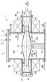
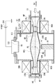
- FIG. 1 is a cross-sectional view schematically showing a film forming apparatus according to an embodiment of a plasma processing apparatus of the present invention.
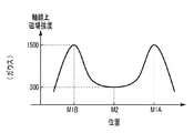
- the graph which shows an example of distribution of the magnetic field intensity on the axis line of a mirror magnetic field.
- the top view which shows the structure of the division ring for electric potential adjustment.
- Sectional drawing which shows the outline of the sputtering device which concerns on other embodiment of the plasma processing apparatus of this invention.
- FIG. 1 shows a film forming apparatus 1 using plasma generation by electron cyclotron resonance (ECR).
- ECR electron cyclotron resonance
- the processing chamber 10 is made of a conductive material such as aluminum alloy or stainless steel, and is connected to a reference potential.
- a top plate 11 is provided above the processing chamber 10, and a supply device 12 that supplies N 2 gas and a supply device 13 that supplies material gas G are provided.
- a stage 50 that holds the wafer W is provided at the bottom of the processing chamber 10.
- the processing chamber 10 is provided with an exhaust port for exhausting the atmosphere in the processing chamber 10, and an exhaust device such as a vacuum pump (not shown) installed outside the processing chamber 10 at the exhaust port. Is connected. The inside of the processing chamber 10 is depressurized by this exhaust device.
- an exhaust device such as a vacuum pump (not shown) installed outside the processing chamber 10 at the exhaust port. Is connected. The inside of the processing chamber 10 is depressurized by this exhaust device.
- a cylindrical member 18A for defining the plasma generation chamber 17A is installed on one side wall of the processing chamber 10 so as to communicate with the processing chamber 10, and the other side wall of the processing chamber 10 faces the plasma generation chamber 17A.
- a cylindrical member 18B for defining the opposed end chamber 17B is installed so as to communicate with the processing chamber 10.
- the central axes of the plasma generation chamber 17A and the opposed end chamber 17B coincide with the axis AX extending in the horizontal direction.
- the outer end of the cylindrical member 18B on the left side of the drawing is sealed with a plate 19.
- a waveguide 15 is connected to the outer end of the cylindrical member 18A on the right side of the drawing, and a microwave formed of a dielectric material such as aluminum oxide is provided between the cylindrical member 18A and the waveguide 15.
- An incident window 16 for MW is provided.
- Current coils 30A and 30B for forming a mirror magnetic field are provided on the outer peripheral sides of the cylindrical members 18A and 18B.
- Limiter members 20A and 20B made of a plate having a circular opening and for defining a region where the plasma PL exists in the processing chamber 10 are installed at the ends of the cylindrical members 18A and 18B on the processing chamber 10 side. ing.
- the limiter members 20A and 20B are arranged in contrast with respect to an intermediate position M2 between the cylindrical member 18A and the cylindrical member 18B.
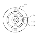
- a potential adjusting split ring 40 having an axis AX as a central axis is provided in the facing end chamber 17B. As shown in FIG. 5, the potential adjusting split ring 40 includes a disk-shaped electrode 41 and ring-shaped electrodes 42 and 43 disposed concentrically on the outside thereof.
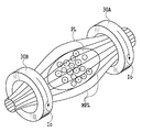
- the current I 0 is passed through the two current coils 30A and 30B in the same direction to form the mirror magnetic field MF.
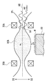
- a microwave MW is supplied through the waveguide 15 to generate plasma.
- a 2.45 GHz microwave undergoes cyclotron resonance with electrons at a magnetic field intensity of 875 gauss, and a plasma PL is generated in the vicinity of the resonance point RP.
- Various conditions are set so that the resonance point RP is arranged in the plasma generation chamber 17A.
- the plasma PL generated near the resonance point RP is constrained by the magnetic field lines ML of the mirror magnetic field MF, and can move freely in the direction of the magnetic field lines MFL.
- the magnetic field intensity on the axis AX becomes maximum at the axial center positions M1A and M1B of the two current coils 30A and 30B, and at an intermediate position M2 between the position M1A and the position M1B on the axis AX.
- the electrons constituting the plasma PL that moves along the magnetic field lines MFL bounce between the two maximum magnetic field parts (M1A, M1B) by the so-called magnetic mirror effect, so that the two maximum magnetic field parts (M1A, M1B). Trapped in between.
- the plasma PL is accelerated from a region where the magnetic field strength of the mirror magnetic field MF is high toward a region where the magnetic field strength of the mirror magnetic field MF is low, but decelerates as the magnetic field strength increases and eventually reaches the maximum magnetic field portion. When it approaches (M1A, M1B), it bounces back. For this reason, the plasma PL is confined in a predetermined confinement region PCR.
- neutral radicals activated from the confinement region PCR selectively reach the wafer W to be processed in the directions D1 and D2 across the magnetic field lines MFL passing through the confinement region PCR. As described above, the wafer W is arranged to face the confinement region PCR.
- the wafer W is disposed below the position M2.
- the distance L between the surface of the wafer W shown in FIG. 2 and the extension (maximum outer periphery position) of the confinement region PCR is activated from the confinement region PCR in a state where charged particles in the plasma PL are confined in the confinement region PCR. Only sex radicals are set to reach the wafer W to be processed without losing activity. This makes it possible to maximize irradiation of neutral active species to the wafer W while greatly reducing ion irradiation from the plasma to the wafer W.
- the role of the limiter members 20A and 20B will be described. If the position of the extension of the confinement region PCR is uncertain, charged particles may enter the wafer W. Since the charged particles are constrained by the lines of magnetic force, the extension of the moving trajectory of the moving plasma is defined by the position of the edge of the opening of the limiter members 20A and 20B. That is, by installing the limiter members 20A and 20B, the extension of the confinement region PCR can be controlled more precisely.
- the material for forming the limiter members 20A and 20B is not particularly limited, but the plasma generated in the plasma generation chamber 17A collides with the limiter members 20A and 20B, and the material for forming the limiter members 20A and 20B is sputtered.
- the limiter members 20A and 20B may be formed of a material containing the forming material of the wafer W, for example, a material containing silicon or the like.
- the role of the potential adjusting split ring 40 will be described.
- a potential gradient is formed in the radial direction centering on the axis AX (direction orthogonal to the axis AX), and the plasma PL confined in the confinement region PCR may easily diffuse in the radial direction.
- the electrode 41 positioned at the center of the potential adjusting split ring 40 is connected to a negative potential
- the electrode 42 is connected to a reference potential
- the electrode 43 disposed on the outermost periphery is connected to a positive potential.
- the film forming apparatus of this embodiment is an apparatus that performs an ALD (Atomic Layer Deposition) process using mirror magnetic field confined plasma.
- ALD Atomic Layer Deposition
- AlN aluminum nitride
- a current of 360 A was passed through the current coils 30A and 30B to generate a magnetic field of 1500 gauss at the maximum magnetic field part (M1A, M1B) and 300 gauss at the mirror magnetic field central part (M2).
- TMA trimethylaluminum
- Al (CH) 3 hereinafter referred to as TMA
- TMA trimethylaluminum
- the pressure in the processing chamber 10 was 1 Torr.
- N 2 gas was flowed at 500 sccm for 1 minute at a pressure of 1 Torr in the processing chamber 10 to remove TMA components remaining without being adsorbed in the processing chamber 10.
- N 2 flowing at 500 sccm the pressure was set to 3 mTorr, a 2.45 GHz microwave MW was introduced into the processing chamber 10, and nitrogen plasma was excited by electron cyclotron resonance for 90 seconds.
- the microwave power was 600W.
- N2 + ions, N + ions, and electrons are confined in the mirror magnetic field and hardly reach the wafer W.
- neutral and active N atom radicals generated in the nitrogen plasma reach the wafer W and react with the adsorbed TMA.
- the CH group was volatilized by CN gas, HN gas, etc., and an aluminum nitride AlN thin film was formed on the surface.
- An aluminum nitride thin film of about 20 nm could be formed by repeating 200 cycles from introduction of TMA to N 2 plasma treatment.
- the present invention it is possible to reduce ion bombardment damage as compared with ordinary plasma treatment, and to form a high-quality aluminum nitride thin film with high breakdown voltage and low leakage current.
- the present invention is not limited to the aluminum nitride shown in this embodiment, and various nitride films can be formed using an organometallic gas usually used in ALD.
- the plasma excitation gas is not N 2 , but may be NH 3 , for example, or a rare gas may be mixed.
- the plasma excitation gas containing oxygen and San ⁇ , O 2 gas, or by a plasma O 2 gas and a rare gas it is possible to form an oxide film.
- FIG. 6 shows a sputtering apparatus according to another embodiment of the plasma processing apparatus of the present invention.
- This sputtering apparatus applies mirror magnetic field confined plasma to a sputtering process.
- a top plate 111 of the processing chamber 10 is provided with a target TG as a magnetron sputtering source held on the lower surface of the backing plate 122.
- a DC power source 200 is connected to the target TG via a backing plate 122.
- a supply device 113 for introducing Ar gas or N 2 gas into the processing chamber 10 is provided on the side wall of the processing chamber 10.
- a magnetron sputtering source is mounted on the processing chamber 10.
- a target TG made of metal hafnium (Hf) is bonded to the backing plate 122.
- a permanent magnet (not shown) was installed in the backing plate 122, and a horizontal magnetic field parallel to the surface of the 500 gauss target TG was formed on the surface of the target TG.
- N 2 gas was introduced into the processing chamber 10, the pressure was set to 5 mTorr, DC power of 300 W was applied to the target TG for 3 seconds, and an HfN thin film having a thickness of about 1 nm was formed on the wafer W by reactive sputtering.
- ions from magnetron plasma are irradiated to the film formation surface, and damage is induced in the film.
- 600 W of 2.45 GHz microwave MW was input to the mirror magnetic field part to excite nitrogen plasma.
- the Hf thin film was nitrided.
- the ion impact damage to the film formation surface is sufficiently smaller than that during sputtering film formation. Therefore, in this nitriding process, damaged parts such as dangling bonds generated during sputtering film formation are nitrided to reduce damage. Is possible.
- a high-quality HfN thin film with high withstand voltage and low leakage current can be formed 20 times with one cycle from Hf deposition to nitridation.
- the sputter film formation and the mirror magnetic field plasma process are alternately performed.
- the sputter film formation and the mirror magnetic field plasma process can be performed simultaneously as compared with a simple reactive sputter process. It was found that damage in the film can be reduced.
- the confinement region PCR has the maximum diameter at the position M2 and has been described as an example in which the diameter decreases toward the current coils 30A and 30B.
- the present invention is not limited to this.
- a magnetic field for correcting the shape of the confinement region PCR can be formed, and the shape of the confinement region PCR can be changed according to the shape and size of the substrate to be processed.
- the wafer W is described as an example of the substrate to be processed, but the present invention can be applied to various substrates such as a glass substrate for a large screen display.
- the potential adjusting split ring 40 is taken as an example of the potential adjusting member.
- the present invention is not limited to this, and any means that can adjust the plasma potential gradient in the confinement region PCR can be used. is there.
- the current coil is used to form the mirror magnetic field, but a permanent magnet may be used instead.
- the stage 50 is stationary, but it is also possible to perform processing while moving the stage 50 relative to the confinement region PCR.
- the opposed end chamber 17B can be a plasma generation chamber.
- a waveguide is newly connected to the opposed end chamber 17B, and an incident window is provided between the opposed end chamber 17B and the new waveguide, and microwaves are introduced through the incident window.
- the potential adjusting split ring 40 is removed.
Landscapes
- Chemical & Material Sciences (AREA)
- Engineering & Computer Science (AREA)
- Organic Chemistry (AREA)
- Chemical Kinetics & Catalysis (AREA)
- Materials Engineering (AREA)
- Mechanical Engineering (AREA)
- Metallurgy (AREA)
- Plasma & Fusion (AREA)
- Physics & Mathematics (AREA)
- General Chemical & Material Sciences (AREA)
- Analytical Chemistry (AREA)
- Electromagnetism (AREA)
- Plasma Technology (AREA)
- Particle Accelerators (AREA)
- Physical Vapour Deposition (AREA)
- Chemical Vapour Deposition (AREA)
- Formation Of Insulating Films (AREA)
Abstract
プラズマで発生したイオンの、衝突による基板のダメージや処理チャンバ内壁のスパッタによる基板の汚染を大幅に抑制しつつ、高品質な薄膜の形成を可能にする。ミラー磁場(MF)とマイクロ波(MW)とによる電子サイクロトロン共鳴によりプラズマを生成するとともに、ミラー磁場(MF)により所定の閉じ込め領域(PCR)に当該プラズマ(PL)を閉じ込め、閉じ込め領域(PCR)から活性化した中性のラジカルが処理すべきウエハ(W)に選択的に到達するように、閉じ込め領域(PCR)を通過する磁力線を横切る方向(D1,D2)においてウエハ(W)を閉じ込め領域(PCR)に対向させて配置する。
Description
本発明は、プラズマ処理装置とプラズマ処理方法とに関する。
半導体製造等におけるプラズマによる薄膜形成プロセスは、プラズマにより反応性に富む様々な活性種を容易に発生させることが出来るため、それら活性種を利用し、基板温度を上げることなく、高品質な薄膜の形成が可能である(例えば、特許文献1参照)。
ところで、プラズマで発生したイオンは、プラズマ電位で加速されてウエハ等の基板に衝突し、ダメージを与える可能性がある。また、処理チャンバの内壁へイオンが照射され、チャンバの内壁材料がスパッタされると、処理すべき基板が汚染される可能性もある。プラズマによる基板へのダメージを低減させるために、プラズマから基板を遠ざけると、活性種が失活してしまい、高品質な薄膜の形成が困難となる。
本発明の目的は、プラズマで発生したイオンの、衝突による基板のダメージや処理チャンバ内壁のスパッタによる基板の汚染を大幅に抑制しつつ、高品質な薄膜の形成を可能にするプラズマ処理装置および方法を提供することにある。
本発明のプラズマ発生装置は、ミラー磁場を形成するミラー磁場形成機構と、マイクロ波を供給するマイクロ波供給機構と、を有し、前記ミラー磁場と前記マイクロ波とによる電子サイクロトロン共鳴によりプラズマを生成するとともに、前記ミラー磁場により所定の閉じ込め領域に当該プラズマを閉じ込めるプラズマ処理装置であって、
前記閉じ込め領域から活性化した中性のラジカルが処理すべき基体に選択的に到達するように、前記閉じ込め領域を通過する磁力線を横切る方向において前記基体を前記閉じ込め領域に対向させて配置する保持機構を有する、ことを特徴とする。
前記閉じ込め領域から活性化した中性のラジカルが処理すべき基体に選択的に到達するように、前記閉じ込め領域を通過する磁力線を横切る方向において前記基体を前記閉じ込め領域に対向させて配置する保持機構を有する、ことを特徴とする。
本発明のプラズマ処理方法は、ミラー磁場とマイクロ波とによる電子サイクロトロン共鳴によりプラズマを生成するとともに、前記ミラー磁場により所定の閉じ込め領域に当該プラズマを閉じ込め、
前記閉じ込め領域から活性化した中性のラジカルが処理すべき基体に選択的に到達するように、前記閉じ込め領域を通過する磁力線を横切る方向において前記基体を前記閉じ込め領域に対向させて配置する、ことを特徴とする。
前記閉じ込め領域から活性化した中性のラジカルが処理すべき基体に選択的に到達するように、前記閉じ込め領域を通過する磁力線を横切る方向において前記基体を前記閉じ込め領域に対向させて配置する、ことを特徴とする。
本発明によれば、プラズマの閉じ込め領域から活性化した中性のラジカルが処理すべき基体に選択的に到達するように、閉じ込め領域を通過する磁力線を横切る方向において基体を前記閉じ込め領域に対向させて配置することにより、プラズマからのイオン照射は可能な限り低減できるとともに、基体への活性種(中性のラジカル)の照射を最大化させることが可能となる。
以下に添付図面を参照しながら、本発明の実施形態について詳細に説明する。なお、本明細書及び図面において、実質的に同一の機能構成を有する構成要素については、同一の符号を付することにより重複説明を省略する。
第1実施形態
図1は、電子サイクロトロン共鳴(ECR)によるプラズマ生成を用いた成膜装置1を示している。後述するように、ミラー磁場閉じ込めプラズマを利用したALD(Atomic Layer Deposition)プロセスを行う装置である。処理チャンバ10は、アルミニウム合金、ステンレス等の導電性材料で形成され、基準電位に接続されている。処理チャンバ10の上部には、天板11が設けられ、N2ガスを供給する供給装置12および材料ガスGを供給する供給装置13が設けられている。処理チャンバ10の底部には、ウエハWを保持するステージ50が設けられている。また、処理チャンバ10には、図示しないが、処理チャンバ10内の雰囲気を排気するための排気口が設けられ、この排気口に処理チャンバ10の外部に設置された図示しない真空ポンプなどの排気装置が接続される。この排気装置により、処理チャンバ10内は減圧される。
図1は、電子サイクロトロン共鳴(ECR)によるプラズマ生成を用いた成膜装置1を示している。後述するように、ミラー磁場閉じ込めプラズマを利用したALD(Atomic Layer Deposition)プロセスを行う装置である。処理チャンバ10は、アルミニウム合金、ステンレス等の導電性材料で形成され、基準電位に接続されている。処理チャンバ10の上部には、天板11が設けられ、N2ガスを供給する供給装置12および材料ガスGを供給する供給装置13が設けられている。処理チャンバ10の底部には、ウエハWを保持するステージ50が設けられている。また、処理チャンバ10には、図示しないが、処理チャンバ10内の雰囲気を排気するための排気口が設けられ、この排気口に処理チャンバ10の外部に設置された図示しない真空ポンプなどの排気装置が接続される。この排気装置により、処理チャンバ10内は減圧される。
処理チャンバ10の一側壁には、プラズマ生成室17Aを画定するための筒状部材18Aが処理チャンバ10と連通するように設置され、処理チャンバ10の他側壁には、プラズマ生成室17Aに対向する対向端部室17Bを画定するための筒状部材18Bが処理チャンバ10と連通するように設置されている。プラズマ生成室17Aおよび対向端部室17Bの中心軸線は、水平方向に延びる軸線AXと一致している。図面左側の筒状部材18Bの外側端部はプレート19により密閉されている。図面右側の筒状部材18Aの外側端部には、導波管15が接続され、筒状部材18Aと導波管15との間には、酸化アルミニウム等の誘電体材料で形成されたマイクロ波MWのための入射窓16が設けられている。筒状部材18Aおよび18Bの外周側には、ミラー磁場を形成するための電流コイル30A,30Bが設けられている。筒状部材18Aおよび18Bの処理チャンバ10側の端部には、円形の開口をもつプレートからなる、処理チャンバ10内でのプラズマPLの存在領域を画定するためのリミッター部材20A,20Bが設置されている。リミッター部材20Aと20Bとは、筒状部材18Aと筒状部材18Bとの間の中間位置M2に関して対照に配置されている。対向端部室17B内には、軸線AXを中心軸にもつ、電位調整用分割リング40が設けられている。電位調整用分割リング40は、図5に示すように、円盤状の電極41、この外側に同心に配置されたリング状の電極42および43からなる。
ここで、本発明の基本コンセプトについて図1~図4を参照して説明する。本発明では、図3に示すように、2つの電流コイル30A,30Bに同じ向きに電流I0を流してミラー磁場MFを形成する。これに加えて、導波管15を通じて図2に示すように、プラズマを生成するためにマイクロ波MWを供給する。ここで、例えば、2.45GHzのマイクロ波は、磁場強度875ガウスで電子とサイクロトロン共鳴し、この共鳴点RP付近でプラズマPLが生成される。共鳴点RPがプラズマ生成室17A内に配置されるように、各種条件が設定さている。共鳴点RP付近で生成されたプラズマPLは、ミラー磁場MFの磁力線MLに拘束され、磁力線MFLの方向には自由に運動できる。図4に示すように、軸線AX上の磁場強度は、2つの電流コイル30A,30Bの軸線方向の中央位置M1A,M1Bで最大となり、軸線AX上の位置M1Aと位置M1Bとの中間位置M2で最小となる。磁力線MFLに沿って運動するプラズマPLを構成する電子は、いわゆる磁気ミラー効果により2つの最大磁場部(M1A,M1B)の間でバウンス運動をすることで、2つの最大磁場部(M1A,M1B)の間に閉じ込められる。具体的には、プラズマPLは、ミラー磁場MFの磁場強度の高い領域からミラー磁場MFの磁場強度の低い領域に向かって加速されるが、磁場強度が高くなるにつれて減速し、やがて、最大磁場部(M1A,M1B)に近づくと跳ね返される。このため、プラズマPLは、所定の閉じ込め領域PCRに閉じ込められる。本発明では、図2に示すように、閉じ込め領域PCRを通過する磁力線MFLを横切る方向D1,D2において、閉じ込め領域PCRから活性化した中性のラジカルが処理すべきウエハWに選択的に到達するように、ウエハWを閉じ込め領域PCRに対向させて配置する。好適には、ウエハWは位置M2の下方に配置される。図2に示すウエハWの表面と閉じ込め領域PCRの外延(最大外周位置)との距離Lが、プラズマPL中の荷電粒子が閉じ込め領域PCRに閉じ込められた状態で、閉じ込め領域PCRから活性化した中性のラジカルのみが活性を失うことなく処理すべきウエハWに到達するように設定される。これにより、プラズマからのウエハWへのイオン照射を大幅に減らしつつ、ウエハWへの中性の活性種の照射を最大化することが可能となる。
次に、リミッター部材20A,20Bの役割について説明する。上記した閉じ込め領域PCRの外延の位置が不確定であると、ウエハWに荷電粒子が入射する可能性がある。荷電粒子は磁力線に拘束されることから、移動するプラズマの移動軌跡の外延は、リミッター部材20A,20Bの開口の縁部の位置で画定される。すなわち、リミッター部材20A,20Bを設置することで、閉じ込め領域PCRの外延をより精密にコントロールすることができる。リミッター部材20A,20Bの形成材料は、特に限定されないが、プラズマ生成室17Aで生成されたプラズマがリミッター部材20A,20Bに衝突し、リミッター部材20A,20Bの形成材料がスパッタされ、このスパッタされた材料がウエハWに付着する可能性もある。このため、リミッター部材20A,20Bを処理すべき基体であるウエハWの形成材料を含む材料、または成膜する薄膜に含まれる材料、例えば、シリコン等を含む材料で形成することも可能である。また、リミッター部材20A,20Bの表面を例えば、シリコン等を含む材料でコーティングしてもよい。同様に、筒状部材18A,18Bの内壁面18fにもプラズマが衝突して筒状部材18A,18Bの形成材料がスパッタされ、このスパッタされた材料がウエハWに付着する可能性もある。このため、筒状部材18A,18Bの形成材料またはコーティング材料をウエハWの形成材料を含む材料、例えば、シリコン等を含む材料で形成してもよい。
次に、電位調整用分割リング40の役割について説明する。ミラー磁場でプラズマを閉じ込めると、軸線AXを中心とする径方向(軸線AXに直交する方向)に電位勾配が形成され、閉じ込め領域PCRに閉じ込められたプラズマPLが径方向に拡散しやすくなることが知られている。このため、例えば、電位調整用分割リング40の中心部に位置する電極41をマイナスの電位に、電極42を基準電位に、最外周に配置された電極43をプラスの電位に接続する。これにより、閉じ込め領域PCRに閉じ込められたプラズマPLに生じる径方向の電位勾配と逆向きの電位勾配を与え、閉じ込め領域PCRに閉じ込められたプラズマPLの電位を平坦化する。これにより、プラズマPLが径方向に拡散することを抑制できて、ウエハWの荷電粒子によるダメージの発生をより一層抑制できる。
本実施形態の成膜装置は、ミラー磁場閉じ込めプラズマを利用したALD(Atomic Layer Deposition)プロセスを行う装置である。ALDにより窒化アルミ(AlN)を成膜する手順の一例について説明する。シリコンからなるウエハWを処理チャンバ10に搬送し、ステージ50は300℃に加熱した。電流コイル30A,30Bには360Aの電流を流し、最大磁場部(M1A,M1B)で1500ガウス、ミラー磁場中央部(M2)で300ガウスの磁場を発生させた。
次に、処理チャンバ10内に材料ガスGであるトリメチルアルミ[Al(CH)3、以下TMA]を流量1sccmで1秒間導入した。処理チャンバ10内の圧力は1Torrとした。これにより、ウエハW表面や処理チャンバ10の内壁面にTMAを吸着させた。次に、N2ガスを処理チャンバ10内の圧力を1Torrとして500sccm、1分間流し、処理チャンバ10内に吸着せずに残留しているTMA成分を除去した。
次に、N2を500sccm流したまま、圧力を3mTorrとし、2.45GHzのマイクロ波MWを処理チャンバ10内に導入し、電子サイクロトロン共鳴により、窒素プラズマを90秒間励起した。マイクロ波パワーは600Wとした。この間、N2+イオンやN+イオン、及び電子はミラー磁場に閉じ込められ、ウエハWにはほとんど到達しない。一方、窒素プラズマ中で発生した中性で活性なN原子ラジカルはウエハW上に到達し、吸着したTMAと反応する。CH基がCNガスやHNガス等で揮発するとともに、表面に窒化アルミAlN薄膜が形成された。TMAの導入からN2プラズマ処理までを1サイクルとし、200サイクル繰り返すことで、20nm程度の窒化アルミ薄膜を形成できた。
本発明により、通常のプラズマ処理に比べ、イオン衝撃ダメージを低減させることができ、高耐圧で、リーク電流の少ない高品質な窒化アルミ薄膜が形成可能となった。
なお、本発明は、本実施例で示した窒化アルミに限らず、ALDで通常用いられる有機金属ガスを用い、様々な窒化膜を形成することが可能である。また、窒化膜の場合、プラズマ励起ガスはN2では無く、例えばNH3でも良くまた希ガスを混ぜても良い。または酸素と酸窒を含むガスでプラズマ励起をすれば酸窒化膜となるし、O2ガス、またはO2ガスと希ガスでプラズマにすることで、酸化膜を形成することも可能である。
第2実施形態
図6に本発明のプラズマ処理装置の他の実施形態に係るスパッタ装置を示す。なお、図6において、図1に示す装置と同様の構成部分には同一の符号を付している。このスパッタ装置は、ミラー磁場閉じ込めプラズマをスパッタプロセスに適用したものである。処理チャンバ10の天板111には、バッキングプレート122の下面に保持されたマグネトロンスパッタ源としてのターゲットTGが設けられている。ターゲットTGは、バッキングプレート122を介してDC電源200が接続されている。また、処理チャンバ10の側壁には、Arガス又はN2ガスを処理チャンバ10内に導入するための供給装置113が設けられている。
図6に本発明のプラズマ処理装置の他の実施形態に係るスパッタ装置を示す。なお、図6において、図1に示す装置と同様の構成部分には同一の符号を付している。このスパッタ装置は、ミラー磁場閉じ込めプラズマをスパッタプロセスに適用したものである。処理チャンバ10の天板111には、バッキングプレート122の下面に保持されたマグネトロンスパッタ源としてのターゲットTGが設けられている。ターゲットTGは、バッキングプレート122を介してDC電源200が接続されている。また、処理チャンバ10の側壁には、Arガス又はN2ガスを処理チャンバ10内に導入するための供給装置113が設けられている。
処理チャンバ10の上部に、マグネトロンスパッタ源が搭載されている。バッキングプレート122に金属ハフニウム(Hf)製のターゲットTGが接着されている。バッキングプレート122内には図示しない永久磁石を設置し、ターゲットTG表面において、500ガウスのターゲットTGの表面に平行な水平磁界を形成した。処理チャンバ10内にN2ガスを導入し、圧力を5mTorrとし、ターゲットTGにDC電力300Wを3秒投入し、ウエハW上へ膜厚1nm程度のHfN薄膜を反応性スパッタにより形成した。
スパッタ成膜時には、成膜表面にマグネトロンプラズマからのイオンが照射され、膜中にダメージが誘起される。次に、600Wの2.45GHzのマイクロ波MWをミラー磁場部に投入し、窒素プラズマを励起した。これにより、Hf薄膜を窒化した。この窒化プロセスでは成膜表面へのイオン衝撃ダメージはスパッタ成膜時に比べて充分少ないので、この窒化プロセスで、スパッタ成膜時に発生したダングリングボンド等のダメージ部分を窒化し、ダメージを低減することが可能である。Hf成膜から窒化を1サイクルとして、20回繰り返し、高耐圧で、リーク電流の少ない高品質なHfN薄膜が形成可能となった。
なお、本実施例ではスパッタ成膜とミラー磁場プラズマプロセスを交互に行ったが、スループットを上げるために、スパッタ成膜とミラー磁場プラズマプロセスを同時に行っても、単純な反応性スパッタプロセスに比べれば、膜中のダメージは低減できることがわかった。
上記実施形態では、閉じ込め領域PCRは、位置M2において最大直径をもち、電流コイル30A、30Bに向けて直径が減少していく場合を例に挙げて説明したが、これに限定されるわけではない。例えば、閉じ込め領域PCRの形状を修正するための磁場を形成し、処理すべき基体の形状や大きさに応じて閉じ込め領域PCRの形状を変更することも可能である。
上記実施形態では、処理すべき基体としてウエハWを例に挙げて説明したが、例えば、大画面ディスプレイ用のガラス基板など、各種の基体に本発明を適用可能である。
上記実施形態では、電位調整用部材として電位調整用分割リング40を例に挙げたが、これに限定されるわけではなく、閉じ込め領域PCRのプラズマの電位勾配を調整できる手段であれば採用可能である。
上記実施形態では、ミラー磁場を形成するために、電流コイルを用いたが、これに代えて、永久磁石を採用することも可能である。
上記実施形態では、ステージ50は静止しているが、閉じ込め領域PCRに対してステージ50を移動させながら処理を行うことも可能である。
上記実施形態では、プラズマ生成室を一箇所に設けて、このプラズマ生成室にマイクロ波を導入する場合について説明したが、本発明はこれに限定されない。たとえば、プラズマ生成室17Aに加えて、対向端部室17Bをプラズマ生成室とすることも可能である。この場合には、対向端部室17Bに新たに導波管を接続するとともに、対向端部室17Bと新たな導波管との間に入射窓を設け、この入射窓を通じてマイクロ波を導入する。なお、電位調整用分割リング40は、除去する。
以上、添付図面を参照しながら本発明の実施形態について詳細に説明したが、本発明はかかる例に限定されない。本発明の属する技術の分野における通常の知識を有する者であれば、特許請求の範囲に記載された技術的思想の範疇内において、各種の変更例または修正例に想到し得ることは明らかであり、これらについても、当然に本発明の技術的範囲に属するものと了解される。
1 成膜装置
10 処理チャンバ
15 導波管
16 入射窓
17A プラズマ生成室
17B 対向端部室
18A,18B 筒状部材
20 リミッター部材
30A,30B 電流コイル
40 電位調整用分割リング
41,42,43 電極
50 ステージ
200 DC電源
RP 共鳴点
PCR 閉じ込め領域
W ウエハ(基体)
10 処理チャンバ
15 導波管
16 入射窓
17A プラズマ生成室
17B 対向端部室
18A,18B 筒状部材
20 リミッター部材
30A,30B 電流コイル
40 電位調整用分割リング
41,42,43 電極
50 ステージ
200 DC電源
RP 共鳴点
PCR 閉じ込め領域
W ウエハ(基体)
Claims (5)
- ミラー磁場を形成するミラー磁場形成機構と、マイクロ波を供給するマイクロ波供給機構と、を有し、前記ミラー磁場と前記マイクロ波とによる電子サイクロトロン共鳴によりプラズマを生成するとともに、前記ミラー磁場により所定の閉じ込め領域に当該プラズマを閉じ込めるプラズマ処理装置であって、
前記閉じ込め領域から活性化した中性のラジカルが処理すべき基体に選択的に到達するように、前記閉じ込め領域を通過する磁力線を横切る方向において前記基体を前記閉じ込め領域に対向させて配置する保持機構を有する、ことを特徴とするプラズマ処理装置。 - 共鳴点が前記閉じ込め領域の所定の軸線方向における一端部に形成され、
前記閉じ込め領域の前記磁力線を横切る方向における外延を画定するリミッター部材をさらに有し、
前記リミッター部材は、前記閉じ込め領域内の磁場強度の最小点と前記共鳴点との間の位置に配置されている、ことを特徴とする請求項1に記載のプラズマ処理装置。 - 前記閉じ込め領域における前記磁力線を横切る方向の電位勾配を平坦化するための電位調整用部材をさらに備える、ことを特徴とする請求項1又は2に記載のプラズマ処理装置。
- 前記プラズマ生成空間を画定する壁面を有し、
前記壁面の少なくとも一部の形成材料が、前記基体の形成材料を含む、ことを特徴とする請求項1ないし3のいずれかに記載のプラズマ処理装置。 - ミラー磁場とマイクロ波とによる電子サイクロトロン共鳴によりプラズマを生成するとともに、前記ミラー磁場により所定の閉じ込め領域に当該プラズマを閉じ込め、
前記閉じ込め領域から活性化した中性のラジカルが処理すべき基体に選択的に到達するように、前記閉じ込め領域を通過する磁力線を横切る方向において前記基体を前記閉じ込め領域に対向させて配置する、ことを特徴とするプラズマ処理方法。
Priority Applications (2)
| Application Number | Priority Date | Filing Date | Title |
|---|---|---|---|
| JP2015516943A JP5909807B2 (ja) | 2014-03-28 | 2014-03-28 | プラズマ処理装置およびプラズマ処理方法 |
| PCT/JP2014/001821 WO2015145486A1 (ja) | 2014-03-28 | 2014-03-28 | プラズマ処理装置およびプラズマ処理方法 |
Applications Claiming Priority (1)
| Application Number | Priority Date | Filing Date | Title |
|---|---|---|---|
| PCT/JP2014/001821 WO2015145486A1 (ja) | 2014-03-28 | 2014-03-28 | プラズマ処理装置およびプラズマ処理方法 |
Publications (1)
| Publication Number | Publication Date |
|---|---|
| WO2015145486A1 true WO2015145486A1 (ja) | 2015-10-01 |
Family
ID=54194093
Family Applications (1)
| Application Number | Title | Priority Date | Filing Date |
|---|---|---|---|
| PCT/JP2014/001821 Ceased WO2015145486A1 (ja) | 2014-03-28 | 2014-03-28 | プラズマ処理装置およびプラズマ処理方法 |
Country Status (2)
| Country | Link |
|---|---|
| JP (1) | JP5909807B2 (ja) |
| WO (1) | WO2015145486A1 (ja) |
Cited By (4)
| Publication number | Priority date | Publication date | Assignee | Title |
|---|---|---|---|---|
| FR3042797A1 (fr) * | 2015-10-27 | 2017-04-28 | Commissariat Energie Atomique | Dispositif pour la fabrication d'une couche en carbone amorphe par plasma a la resonance cyclotron electronique |
| JP2020045520A (ja) * | 2018-09-19 | 2020-03-26 | トヨタ自動車株式会社 | プラズマcvd装置 |
| EP3710614A1 (fr) * | 2017-11-17 | 2020-09-23 | Centre National de la Recherche Scientifique | Réacteur de dépôt de couches et procédé de dépôt associé |
| WO2021090794A1 (ja) * | 2019-11-06 | 2021-05-14 | 株式会社クリエイティブコーティングス | 成膜方法及び成膜装置 |
Families Citing this family (1)
| Publication number | Priority date | Publication date | Assignee | Title |
|---|---|---|---|---|
| CN106304603A (zh) * | 2016-09-27 | 2017-01-04 | 中国科学院合肥物质科学研究院 | 一种中性束注入器离子源场反向位形等离子体射频驱动器 |
Citations (6)
| Publication number | Priority date | Publication date | Assignee | Title |
|---|---|---|---|---|
| JPS62170475A (ja) * | 1986-01-24 | 1987-07-27 | Hitachi Ltd | プラズマ処理装置 |
| JPH01238020A (ja) * | 1988-03-18 | 1989-09-22 | Hitachi Ltd | プラズマ処理装置、及びその処理システム |
| JPH0227718A (ja) * | 1988-07-15 | 1990-01-30 | Mitsubishi Electric Corp | プラズマ処理方法およびそれに用いるプラズマ処理装置 |
| JPH03132027A (ja) * | 1989-10-18 | 1991-06-05 | Sumitomo Metal Ind Ltd | プラズマ装置及びその操業方法 |
| JPH05198533A (ja) * | 1992-01-20 | 1993-08-06 | Sony Corp | ドライエッチング方法 |
| JPH0774112A (ja) * | 1993-09-27 | 1995-03-17 | Hitachi Ltd | プラズマ処理方法、及びその装置 |
Family Cites Families (3)
| Publication number | Priority date | Publication date | Assignee | Title |
|---|---|---|---|---|
| JPH0770510B2 (ja) * | 1984-06-12 | 1995-07-31 | 富士通株式会社 | プラズマ処理装置 |
| JPS62291031A (ja) * | 1986-06-11 | 1987-12-17 | Hitachi Ltd | プラズマ処理装置 |
| JP2876318B2 (ja) * | 1989-01-20 | 1999-03-31 | 三洋電機株式会社 | 薄膜形成方法 |
-
2014
- 2014-03-28 WO PCT/JP2014/001821 patent/WO2015145486A1/ja not_active Ceased
- 2014-03-28 JP JP2015516943A patent/JP5909807B2/ja active Active
Patent Citations (6)
| Publication number | Priority date | Publication date | Assignee | Title |
|---|---|---|---|---|
| JPS62170475A (ja) * | 1986-01-24 | 1987-07-27 | Hitachi Ltd | プラズマ処理装置 |
| JPH01238020A (ja) * | 1988-03-18 | 1989-09-22 | Hitachi Ltd | プラズマ処理装置、及びその処理システム |
| JPH0227718A (ja) * | 1988-07-15 | 1990-01-30 | Mitsubishi Electric Corp | プラズマ処理方法およびそれに用いるプラズマ処理装置 |
| JPH03132027A (ja) * | 1989-10-18 | 1991-06-05 | Sumitomo Metal Ind Ltd | プラズマ装置及びその操業方法 |
| JPH05198533A (ja) * | 1992-01-20 | 1993-08-06 | Sony Corp | ドライエッチング方法 |
| JPH0774112A (ja) * | 1993-09-27 | 1995-03-17 | Hitachi Ltd | プラズマ処理方法、及びその装置 |
Non-Patent Citations (1)
| Title |
|---|
| MASAAKI INUTAKE: "Comparison of density and magnetic field fluctuation radial direction distribution by microwave reflectometer and probe measurement", HEISEI 7 NEN TO 8 NENDO KAGAKU KENKYUHI HOJOKIN (KIBAN KENKYU (B)(2)) KENKYU SEIKA HOKOKUSHO, March 1997 (1997-03-01), pages 1 - 73 * |
Cited By (8)
| Publication number | Priority date | Publication date | Assignee | Title |
|---|---|---|---|---|
| FR3042797A1 (fr) * | 2015-10-27 | 2017-04-28 | Commissariat Energie Atomique | Dispositif pour la fabrication d'une couche en carbone amorphe par plasma a la resonance cyclotron electronique |
| WO2017072434A1 (fr) * | 2015-10-27 | 2017-05-04 | Commissariat A L'energie Atomique Et Aux Energies Alternatives | Dispositif pour la fabrication d'une couche en carbone amorphe par plasma a la resonance cyclotron electronique |
| US11075061B2 (en) | 2015-10-27 | 2021-07-27 | Commissariat A L'energie Atomique Et Aux Energies Alternatives | Device for producing an amorphous carbon layer by electron cyclotron resonance plasma |
| EP3710614A1 (fr) * | 2017-11-17 | 2020-09-23 | Centre National de la Recherche Scientifique | Réacteur de dépôt de couches et procédé de dépôt associé |
| JP2020045520A (ja) * | 2018-09-19 | 2020-03-26 | トヨタ自動車株式会社 | プラズマcvd装置 |
| WO2021090794A1 (ja) * | 2019-11-06 | 2021-05-14 | 株式会社クリエイティブコーティングス | 成膜方法及び成膜装置 |
| JPWO2021090794A1 (ja) * | 2019-11-06 | 2021-05-14 | ||
| JP7112793B2 (ja) | 2019-11-06 | 2022-08-04 | 株式会社クリエイティブコーティングス | 成膜方法及び成膜装置 |
Also Published As
| Publication number | Publication date |
|---|---|
| JPWO2015145486A1 (ja) | 2017-04-13 |
| JP5909807B2 (ja) | 2016-04-27 |
Similar Documents
| Publication | Publication Date | Title |
|---|---|---|
| CN106663609B (zh) | 用以实现高密度高sp3含量层的高功率脉冲磁控溅镀工艺 | |
| TWI499682B (zh) | 電漿處理腔室以及沉積薄膜的方法 | |
| KR101331420B1 (ko) | 기판 처리 장치 및 반도체 장치의 제조 방법 | |
| JP5909807B2 (ja) | プラズマ処理装置およびプラズマ処理方法 | |
| JP7236477B2 (ja) | Pvd装置 | |
| JP2020514554A (ja) | プラズマリアクタ及びプラズマリアクタでのダイヤモンドライクカーボンの堆積又は処理 | |
| US10483118B2 (en) | Etching method | |
| JP6880233B2 (ja) | 回転式サセプタ向けのプラズマ源 | |
| US8911602B2 (en) | Dual hexagonal shaped plasma source | |
| TWI713414B (zh) | 基板處理裝置、半導體裝置之製造方法及記錄媒體 | |
| CN120591743A (zh) | 控制脉冲直流pvd形成的材料层中应力变化的方法及设备 | |
| JP2004292934A (ja) | イオン窒化装置およびこれを用いた成膜装置 | |
| JP2024050576A (ja) | 改良されたプラズマ制御のためのem源 | |
| US12288670B2 (en) | Pulsed DC power for deposition of film | |
| TW201725603A (zh) | 電漿處理裝置 | |
| JP6905699B2 (ja) | プラズマ処理装置、プラズマ処理方法および半導体製造方法 | |
| KR102617710B1 (ko) | 기판 처리장치 | |
| KR20190119274A (ko) | 스퍼터 건 및 이를 포함하는 스퍼터링 증착 장치 | |
| WO2025101413A1 (en) | Apparatus and method of damage mitigation and step coverage enhancement | |
| RU2395134C2 (ru) | Устройство для плазмохимической обработки материалов | |
| WO2012070195A1 (ja) | スパッタリング方法 | |
| JPH05222538A (ja) | マイクロ波プラズマ処理装置 |
Legal Events
| Date | Code | Title | Description |
|---|---|---|---|
| ENP | Entry into the national phase |
Ref document number: 2015516943 Country of ref document: JP Kind code of ref document: A |
|
| 121 | Ep: the epo has been informed by wipo that ep was designated in this application |
Ref document number: 14887676 Country of ref document: EP Kind code of ref document: A1 |
|
| NENP | Non-entry into the national phase | ||
| 122 | Ep: pct application non-entry in european phase |
Ref document number: 14887676 Country of ref document: EP Kind code of ref document: A1 |