WO2015129717A1 - Fet並列回路セルおよび疑似高電圧fetモジュール - Google Patents
Fet並列回路セルおよび疑似高電圧fetモジュール Download PDFInfo
- Publication number
- WO2015129717A1 WO2015129717A1 PCT/JP2015/055324 JP2015055324W WO2015129717A1 WO 2015129717 A1 WO2015129717 A1 WO 2015129717A1 JP 2015055324 W JP2015055324 W JP 2015055324W WO 2015129717 A1 WO2015129717 A1 WO 2015129717A1
- Authority
- WO
- WIPO (PCT)
- Prior art keywords
- circuit
- sic
- misfet
- fet
- converter
- Prior art date
- Legal status (The legal status is an assumption and is not a legal conclusion. Google has not performed a legal analysis and makes no representation as to the accuracy of the status listed.)
- Ceased
Links
Images





Classifications
-
- H—ELECTRICITY
- H02—GENERATION; CONVERSION OR DISTRIBUTION OF ELECTRIC POWER
- H02M—APPARATUS FOR CONVERSION BETWEEN AC AND AC, BETWEEN AC AND DC, OR BETWEEN DC AND DC, AND FOR USE WITH MAINS OR SIMILAR POWER SUPPLY SYSTEMS; CONVERSION OF DC OR AC INPUT POWER INTO SURGE OUTPUT POWER; CONTROL OR REGULATION THEREOF
- H02M1/00—Details of apparatus for conversion
- H02M1/08—Circuits specially adapted for the generation of control voltages for semiconductor devices incorporated in static converters
-
- H—ELECTRICITY
- H03—ELECTRONIC CIRCUITRY
- H03K—PULSE TECHNIQUE
- H03K17/00—Electronic switching or gating, i.e. not by contact-making and –breaking
- H03K17/10—Modifications for increasing the maximum permissible switched voltage
- H03K17/102—Modifications for increasing the maximum permissible switched voltage in field-effect transistor switches
-
- H—ELECTRICITY
- H03—ELECTRONIC CIRCUITRY
- H03K—PULSE TECHNIQUE
- H03K17/00—Electronic switching or gating, i.e. not by contact-making and –breaking
- H03K17/12—Modifications for increasing the maximum permissible switched current
- H03K17/122—Modifications for increasing the maximum permissible switched current in field-effect transistor switches
-
- H—ELECTRICITY
- H03—ELECTRONIC CIRCUITRY
- H03K—PULSE TECHNIQUE
- H03K2217/00—Indexing scheme related to electronic switching or gating, i.e. not by contact-making or -breaking covered by H03K17/00
- H03K2217/0009—AC switches, i.e. delivering AC power to a load
-
- H—ELECTRICITY
- H10—SEMICONDUCTOR DEVICES; ELECTRIC SOLID-STATE DEVICES NOT OTHERWISE PROVIDED FOR
- H10D—INORGANIC ELECTRIC SEMICONDUCTOR DEVICES
- H10D30/00—Field-effect transistors [FET]
- H10D30/60—Insulated-gate field-effect transistors [IGFET]
- H10D30/64—Double-diffused metal-oxide semiconductor [DMOS] FETs
- H10D30/66—Vertical DMOS [VDMOS] FETs
-
- H—ELECTRICITY
- H10—SEMICONDUCTOR DEVICES; ELECTRIC SOLID-STATE DEVICES NOT OTHERWISE PROVIDED FOR
- H10D—INORGANIC ELECTRIC SEMICONDUCTOR DEVICES
- H10D30/00—Field-effect transistors [FET]
- H10D30/60—Insulated-gate field-effect transistors [IGFET]
- H10D30/64—Double-diffused metal-oxide semiconductor [DMOS] FETs
- H10D30/66—Vertical DMOS [VDMOS] FETs
- H10D30/668—Vertical DMOS [VDMOS] FETs having trench gate electrodes, e.g. UMOS transistors
-
- H—ELECTRICITY
- H10—SEMICONDUCTOR DEVICES; ELECTRIC SOLID-STATE DEVICES NOT OTHERWISE PROVIDED FOR
- H10D—INORGANIC ELECTRIC SEMICONDUCTOR DEVICES
- H10D62/00—Semiconductor bodies, or regions thereof, of devices having potential barriers
- H10D62/80—Semiconductor bodies, or regions thereof, of devices having potential barriers characterised by the materials
- H10D62/83—Semiconductor bodies, or regions thereof, of devices having potential barriers characterised by the materials being Group IV materials, e.g. B-doped Si or undoped Ge
- H10D62/832—Semiconductor bodies, or regions thereof, of devices having potential barriers characterised by the materials being Group IV materials, e.g. B-doped Si or undoped Ge being Group IV materials comprising two or more elements, e.g. SiGe
- H10D62/8325—Silicon carbide
-
- Y—GENERAL TAGGING OF NEW TECHNOLOGICAL DEVELOPMENTS; GENERAL TAGGING OF CROSS-SECTIONAL TECHNOLOGIES SPANNING OVER SEVERAL SECTIONS OF THE IPC; TECHNICAL SUBJECTS COVERED BY FORMER USPC CROSS-REFERENCE ART COLLECTIONS [XRACs] AND DIGESTS
- Y02—TECHNOLOGIES OR APPLICATIONS FOR MITIGATION OR ADAPTATION AGAINST CLIMATE CHANGE
- Y02B—CLIMATE CHANGE MITIGATION TECHNOLOGIES RELATED TO BUILDINGS, e.g. HOUSING, HOUSE APPLIANCES OR RELATED END-USER APPLICATIONS
- Y02B70/00—Technologies for an efficient end-user side electric power management and consumption
- Y02B70/10—Technologies improving the efficiency by using switched-mode power supplies [SMPS], i.e. efficient power electronics conversion e.g. power factor correction or reduction of losses in power supplies or efficient standby modes
Definitions
- the present invention relates to an FET parallel circuit cell and a pseudo high voltage FET module, and more particularly to an FET parallel circuit cell and a pseudo high voltage FET module applicable to a high voltage pulse switching power supply.
- SiC silicon carbide
- SiC has a very large dielectric breakdown electric field compared to Si. Therefore, even if the drift layer film thickness for giving a withstand voltage is formed relatively thin and the carrier concentration is formed relatively high, it does not break.
- Si-MISFET Metal-Insulator-Semiconductor-Field-Effect-Transistor
- a semiconductor switch element is used for a high voltage pulse generation power source that performs high repetition operation, but in order to flow a large current while ensuring a withstand voltage, a circuit connected in series and in parallel is used (for example, refer nonpatent literature 1.).
- a conventional pulse power supply using a Si-MISFET of 600V or higher as a switching element is suitable for high-speed response and high repetition frequency, but has high on-resistance and cannot flow a large current.
- an insulated gate bipolar transistor IGBT: Insulated Gate Bipolar Transistor
- IGBT Insulated Gate Bipolar Transistor
- Si-MISFET has a high on-resistance, so it does not perform any special timing adjustment beyond circuit pattern adjustment.
- a conventional control method among the switch elements connected in series when the timing is shifted, When the partial pressure balance is lost, a high voltage is applied locally, and there is a risk that the switch element is destroyed.
- An object of the present invention is to provide a SiC-MISFET parallel circuit cell and a pseudo high voltage FET module in which a plurality of stages of the FET parallel circuit cells are connected in series and capable of switching a large current at a frequency in the MHz range.
- a plurality of SiC-MISFETs connected in parallel, a plurality of gate drive circuits respectively connected to the gates of the plurality of SiC-MISFETs,
- An FET parallel circuit cell including an OE converter that supplies a gate drive signal to a gate drive circuit, and a plurality of the gate drive circuits and an isolated DC / DC converter that supplies power to the OE converter is provided.
- a pseudo high voltage FET module includes a pulse delay circuit that can be controlled on / off substantially simultaneously.
- a plurality of SiC-MISFET AC load circuits connected in parallel, a plurality of gate drive circuits respectively connected to the gates of the plurality of SiC-MISFET AC load circuits
- an MIS relay circuit cell comprising an OE converter that supplies a gate drive signal to a gate drive circuit, and a plurality of the gate drive circuits and an isolated DC / DC converter that supplies power to the OE converter.
- a switching circuit in which a plurality of MIS type relay circuit cells are connected in series and a plurality of the MIS type relay circuit cells constituting the switching circuit are connected to each other, and a plurality of the MIS types are connected.
- a pseudo high voltage FET module comprising a pulse delay circuit capable of controlling on / off of substantially simultaneous relay circuit cells.
- the present invention it is possible to provide a SiC-MISFET parallel circuit cell and a pseudo high voltage FET module in which a plurality of stages of the FET parallel circuit cells are serialized and capable of switching a large current at an MHz class frequency.
- the typical circuit block diagram of the FET parallel circuit cell which concerns on basic technology.
- the typical circuit block block diagram of the pseudo high voltage FET module which concerns on a basic technique.
- the typical circuit block diagram of the FET parallel circuit cell which concerns on 1st Embodiment.
- the typical circuit block block diagram of the pseudo high voltage FET module which concerns on 1st Embodiment.
- the typical circuit block diagram of the FET parallel circuit cell which concerns on 2nd Embodiment.
- the typical block block diagram of the FET parallel circuit cell which concerns on 3rd Embodiment to which the transformer insulation type DC / DC converter is applied.
- the typical block block diagram of the FET parallel circuit cell which concerns on 3rd Embodiment to which a wireless electric power feeding type DC / DC converter is applied.
- FIG. 4 is a schematic cross-sectional structure diagram of a SiC DIMISFET, which is an example of a semiconductor device applicable to the pseudo high voltage FET module according to the embodiment. It is an example of the semiconductor device applicable to the pseudo high voltage FET module which concerns on embodiment, Comprising: The typical cross-section figure of SiC TMISFET.
- the FET parallel circuit cell 10A includes a plurality of Si-MISFETs Q M1 , Q M2 , Q M3 ,..., Q M6 and a plurality of Si-MISFETs Q M1 , Q M2 connected in parallel. , Q M3 ,..., Q M6 , a plurality of gate drive circuits 12 1 A, 12 2 A, 12 3 A,..., 12 6 A and a plurality of gate drive circuits 12 1 A, 12 2, respectively.
- OE converter 14A supplies a gate drive signal to a, a plurality of gate drive circuits 12 1 a, 12 2 a, 12 3 a, ..., 12 6 a and OE converter And an isolated DC / DC converter 16A that supplies power to 14A.
- An ON / OFF signal is supplied to the OE converter 14A via the optical fiber cable 18A, while a DC voltage of, for example, + 24V is supplied to the insulated DC / DC converter 16A via the gate drive voltage supply line 20A. Is supplied.
- Si-MISFETQ M1, Q M2, Q M3, ..., the drain of Q M6 are commonly connected to the positive power terminal P (+), Si-MISFETQ M1, Q M2, Q M3, ..., the source of Q M6 is Are connected in common to the negative power terminal N ( ⁇ ).
- the pseudo high voltage FET module 1A includes a switching circuit 4A in which a plurality of FET parallel circuit cells 10A are connected in series, and a plurality of FET parallel circuits constituting the switching circuit 4A.
- cell 10 1 a, 10 2 a, 10 3 a, ..., 10 8 respectively a fiber optic cable 18 1 a, 18 2 a, 18 3 a, ..., 18 8 via the a connected EO converter 22 1 A, 22 2 A, 22 3 A,..., 22 8 A.
- the optical fiber cables 18 1 A, 18 2 A, 18 3 A,..., 18 8 A can be bundled as an optical fiber cable bundle 180A.
- the switching circuit 4A connected in series in a plurality of stages is connected to the global drain terminal D (+) on the drain side of the FET parallel circuit cell 10 1 A, and the global source terminal S ( ⁇ ) on the source side of the FET parallel circuit cell 10 8 A. Connected to.
- the electrical input sides of the EO converters 22 1 A, 22 2 A, 22 3 A,..., 22 8 A are connected to the global gate terminal G through the buffer circuit 21A.
- a multi-series circuit of Si-MISFETs Q M1 , Q M2 , Q M3 ,..., Q M6 is configured. That is, 6 parallel Si-MISFETQ M1, Q M2, Q M3, ..., 1 FET parallel circuit cell 10 includes a Q M6 A, 10 2 A, 10 3 A, ..., a 10 8 A connected to the 8 series, the pseudo A high voltage FET module 1A is realized.
- the pseudo-high-voltage FET module 1A according to the basic technique, Si-MISFETQ M1, Q M2 , Q M3, ..., as Q M6, rated switching voltage 700 V, is applied to Si-MISFET rated switching current 100A, Switching performance of a rated switching voltage of 5.6 kV and a rated switching current of 600 A can be realized.
- the FET parallel circuit cell 10 includes a plurality of SiC-MISFETs Q S1 , Q S2 , Q S3 ,..., Q S6 and a plurality of SiC-MISFET Qs connected in parallel.
- the OE converter 14 supplies a gate drive signal to 6, a plurality of gate drive circuits 12 1, 12 2, 12 3, ..., 12 6 and insulated supplies power to OE converter 14 And a DC / DC converter 16.
- the OE converter 14 is supplied with an ON / OFF signal via an optical fiber cable 18, while the insulated DC / DC converter 16 is supplied with a DC voltage of, for example, + 24V via a gate drive voltage supply line 20. Is supplied. SiC-MISFETQ S1, Q S2, Q S3, ..., the drain of Q S6 are commonly connected to the positive power terminal P (+), SiC-MISFETQ S1, Q S2, Q S3, ..., the source of Q S6 is Are connected in common to the negative power terminal N ( ⁇ ).
- the OE converter 14 is a photoelectric conversion element, and for example, a photo coupler, a fiber coupler, or the like is applicable.
- applicable SiC-MISFETs Q S1 , Q S2 , Q S3 ,..., Q S6 have, for example, a rated drain-source voltage of 1200 V and a rated drain pulse current of 80 A on a general specification.
- SiC-MISFET has a large avalanche breakdown margin with respect to the rated drain-source voltage.
- a 1200-V SiC-MISFET operates without avalanche breakdown up to about 1700 V with respect to a pulsed voltage.
- a 3300V SiC-MISFET operates without avalanche breakdown up to about 4000V for a pulsed voltage.
- the reason why the avalanche breakdown voltage is set high in the SiC-MISFET is as follows.
- a gate insulating film (132: see FIG. 12 and FIG. 13) formed of SiO 2 obtained by oxidizing SiC, a part of carbon (C) atoms remains at the SiC / SiO 2 interface, and the interface state. Reduce density. For this reason, it is difficult to increase the thickness of the gate insulating film (SiO 2 ).
- the pseudo high voltage FET module 1 includes a switching circuit 4 in which a plurality of FET parallel circuit cells 10 are connected in series, and a plurality of FETs constituting the switching circuit 4.
- each optical fiber cable 18 1, 18 2, 18 3, ..., 18 a plurality of EO converter 22 connected 8 via a 1, 22 2, 22 3, ..., 22 8, a plurality of EO converter 22 1, 22 2, 22 3, ..., are connected to 22 8, more FET parallel circuit cells 10 1 constituting the switching circuit 4, 10 2, 10 3, ..., 10 8 substantially simultaneously oN / oFF controllable plurality of pulse delay circuit 24 1, 24 2, 24 3, ..., and a 24 8.
- the optical fiber cables 18 1 , 18 2 , 18 3 ,..., 18 8 can be bundled as an optical fiber cable bundle 180.
- the pulse delay circuits 24 1 , 24 2 , 24 3 ,..., 24 8 can be configured by, for example, FPGA (Field Programmable Gate Array) circuits.
- the switching circuit 4 in which a plurality of FET parallel circuit cells 10 1 , 10 2 , 10 3 ,..., 10 8 are connected in series is connected to the global drain terminal D (+) on the drain side of the FET parallel circuit cell 10 1.
- the FET parallel circuit cell 10 8 is connected to the global source terminal S ( ⁇ ) on the source side.
- the input sides of the pulse delay circuits 24 1 , 24 2 , 24 3 ,..., 24 8 are connected to the global gate terminal G through the buffer circuit 21.
- the rise characteristics of m ⁇ n SiC-MISFETs arranged in m rows and n columns are measured to extract from the SiC-MISFET having the fastest rise time to the m-th fastest SiC-MISFET.
- FIG. 3 as shown in- Figure 4, SiC-MISFETQ S1, Q S2, Q S3, ..., a plurality of FET parallel circuit cells 10 1 by Q S6, 10 2, 10 3, ... 10 8 are connected in series to realize the pseudo high voltage FET module 1.
- SiC-MISFET is smaller the normalized on-resistance than 1/10 as compared with the Si-MISFET, each FET parallel circuit cells 10 1, 10 2, 10 3, ..., to substantially simultaneously turned on / off 10 8 Therefore, it is necessary to take special care and countermeasures. This is because if the FET parallel circuit cells 10 1 , 10 2 , 10 3 ,..., 10 8 have different switching timings, the partial pressure balance is lost and an excessive voltage is generated in a specific FET parallel circuit cell. .
- each FET parallel circuit cell 10 1 , 10 2 , 10 3 ,..., 10 8 is within plus or minus several ns, for example plus or minus 1 ns. Can be turned on / off within. Therefore, the FET parallel circuit cells 10 1 , 10 2 , 10 3 ,..., 10 8 can be turned on / off substantially simultaneously.
- the pseudo high voltage FET module 1 having a rated switching voltage of 9.6 kV and a rated switching current of 480 A can be realized.
- SiC can maintain an off state even at 200 ° C. or higher as compared with Si, the frequency can be increased repeatedly with the same heat dissipation system as in the prior art.
- the FET parallel circuit cell of the switching circuit in which a plurality of FET parallel circuit cells are serially connected can be controlled on / off substantially simultaneously, and the partial pressure balance of the FET parallel circuit cell can be controlled. It is possible to provide a pseudo high voltage FET module that can be well maintained and can switch a large current at a frequency in the MHz range.
- an FET parallel circuit cell 10 As shown in FIG. 5, an FET parallel circuit cell 10 according to the second exemplary embodiment is connected in parallel with SiC-MISFETs Q S1 , Q S2 , Q S3 ,..., Q S6 and absorbs a surge voltage. 26.
- the surge absorbing circuit 26 may include a constant voltage element, an avalanche diode (ABD: Avalanche Breakdown Diode), or the like.
- ABS Avalanche Breakdown Diode
- SiC-MISFETQ S1, Q S2, Q S3, ..., Q S6 and the surge absorption circuit more FET parallel circuit cells 10 1 with a 26, 10 2, 10 3 ,..., 10 8 can be connected in series to realize the pseudo high voltage FET module 1.
- a SiC-MISFET having a rated drain-source voltage of 1200 V and a rated drain pulse current of 80 A is applied as the SiC-MISFETs Q S1 , Q S2 , Q S3 ,..., Q S6
- the rated switching voltage is 9.6 kV and the rated switching current is 480 A
- the pseudo high voltage FET module 1 can be realized.
- SiC-MISFET has a large margin for the rated drain-source voltage.
- a SiC-MISFET with a withstand voltage of 1200 V operates without avalanche breakdown up to about 1700 V with respect to a pulse voltage.
- a 3300V SiC-MISFET operates without avalanche breakdown up to about 4000V for a pulsed voltage.
- the 2 FET also each in the exemplary pseudo-high-voltage FET module according to the parallel circuit cells 10 1, 10 2, 10 3, ..., the pulse delay circuit 24 every 10 8 1, 24 2, 24 3, ..., 24 8 by installing, by adjusting the on-delay time and oFF-delay time, the FET parallel circuit cells 10 1, 10 2, 10 3, ..., and the circuit is substantially almost simultaneously turned on / off configuration 10 8 can do.
- FET parallel circuit cells 10 1, 10 2, 10 3, ..., 10 8 for example, by installing a surge absorption circuit 26 due ABD (avalanche breakdown diode), Even if the parallel FET circuit cells 10 1 , 10 2 , 10 3 ,..., 10 8 are not suddenly completely turned on / off at the same time, they are turned on / off within ⁇ 10 ns, for example, within ⁇ 20 ns. Thus, the pseudo high voltage FET module 1 capable of normal operation can be realized.
- ABD avalanche breakdown diode
- the surge absorbing circuit 26 In the surge absorbing circuit 26, four ABDs having a breakdown voltage of about 350V are connected in series, and it is possible to avoid applying an excessive voltage exceeding 1400V to the SiC-MISFET.
- an FET parallel circuit cell capable of absorbing a voltage surge higher than an avalanche breakdown voltage by ABD.
- the voltage value per unit FET parallel circuit cell can be defined by the avalanche breakdown voltage of the ABD when ABDs are connected in parallel.
- the avalanche breakdown voltage of the ABD is designed to be higher than the rated drain-source voltage of the SiC-MISFET and lower than the avalanche breakdown voltage of the SiC-MISFET.
- the FET parallel circuit cell of the switching circuit in which a plurality of FET parallel circuit cells are serially connected can be controlled on / off substantially at the same time. It is possible to provide a pseudo high voltage FET module that can maintain a good pressure balance and can switch a large current at a frequency in the MHz range.
- FIG. 1 A schematic block configuration of the FET parallel circuit cell 34A according to the third embodiment to which the transformer insulation type DC / DC converter 28A is applied is expressed as shown in FIG.
- the FET parallel circuit cell 34A includes a transformer insulated DC / DC converter 28A, a SiC-MISFET drive circuit 30A connected to the transformer insulated DC / DC converter 28A, and a 6 connected to the SiC-MISFET drive circuit 30A. And a parallel SiC-MISFET circuit 32A.
- the transformer-isolated DC / DC converter 28A supplies a DC voltage V DD to the SiC-MISFET drive circuit 30A, and the SiC-MISFET drive circuit 30A sends a gate drive signal FD to the 6-parallel SiC-MISFET circuit 32A. Supply.
- the SiC-MISFET drive circuit 30A corresponds to the plurality of gate drive circuits 12 1 , 12 2 , 12 3 ,..., 12 6 shown in FIGS. Further, the 6-parallel SiC-MISFET circuit 32A corresponds to the SiC-MISFETs Q S1 , Q S2 , Q S3 ,..., Q S6 shown in FIGS.
- the insulation breakdown voltage V BM is several tens of kV at the maximum.
- FIG. 1 A schematic block configuration of the FET parallel circuit cell 34 according to the third embodiment to which the wireless power feeding type isolated DC / DC converter 28 is applied is expressed as shown in FIG.
- the FET parallel circuit cell 34 includes a wireless power feeding type isolated DC / DC converter 28 and a SiC- connected to the insulated DC / DC converter 28.
- a MISFET drive circuit 30 and a 6 parallel SiC-MISFET circuit 32 connected to the SiC-MISFET drive circuit 30 are provided.
- the isolated DC / DC converter 28 supplies the DC voltage V DD to the SiC-MISFET drive circuit 30, and the SiC-MISFET drive circuit 30 supplies the gate drive signal FD to the 6-parallel SiC-MISFET circuit 32. Supply.
- the SiC-MISFET drive circuit 30 corresponds to the plurality of gate drive circuits 12 1 , 12 2 , 12 3 ,..., 12 6 shown in FIGS. Further, the 6-parallel SiC-MISFET circuit 32 corresponds to the SiC-MISFETs Q S1 , Q S2 , Q S3 ,..., Q S6 shown in FIGS.
- the wireless power feeding type isolated DC / DC converter 28 can wirelessly feed power from an oscillation circuit 38, a primary coil L1 connected to the oscillation circuit 38, and the primary coil L1.
- a secondary coil L2 and a rectifier circuit 40 connected to the secondary coil L2 are provided.
- the primary side coil L1 and the secondary side coil L2 are spaced apart by a creeping distance L S.
- the creepage distance L S between the primary coil L1 and the secondary coil L2 is set according to the value of the dielectric breakdown electric field.
- a housing 36 that includes the oscillation circuit 38 and the primary coil L1 and can control the withstand voltage V BS of the isolated DC / DC converter 28 may be provided.
- the container 36 may be formed of resin or ceramics.
- the withstand voltage value can be controlled by the thickness of the resin or ceramic. For example, when polyethylene resin is used, the dielectric breakdown electric field is about 50 kV / mm.
- the value of the insulation withstand voltage V BS is several hundred kV or more at the maximum.
- a dielectric breakdown electric field of 1 MV / 8 mm and about 120 kV / mm or more by using a resin box as the container 36.
- the resin for example, Teflon (registered trademark), polyethylene, or the like is applicable.
- a pseudo high voltage FET module can be realized by connecting a plurality of FET parallel circuit cells in series as in the first and second embodiments.
- a pseudo high voltage FET module having a rated switching voltage of several hundred kV or more by mounting an ultra-high withstand voltage insulated DC / DC converter using a wireless power feeding circuit.
- An FET module can be realized.
- the FET parallel circuit cell of the switching circuit in which a plurality of FET parallel circuit cells are serially connected can be controlled on / off substantially at the same time. It is possible to provide a pseudo high voltage FET module for an ultra-high withstand voltage that can maintain a good current and can switch a large current at a frequency in the MHz range.
- the ABD when the ABD is connected to the FET parallel circuit cell, it is possible to provide an ultra-high withstand voltage FET parallel circuit cell capable of absorbing a voltage surge higher than the avalanche breakdown voltage.
- the FET parallel circuit cell 34 is connected to a wireless power feeding type insulated DC / DC converter 28 and an insulated DC / DC converter 28.
- the SiC-MISFET drive circuit 30 and a 6 parallel SiC-MISFET circuit 32 connected to the SiC-MISFET drive circuit 30 are provided.
- the SiC-MISFET drive circuit 30 corresponds to the plurality of gate drive circuits 12 1 , 12 2 , 12 3 ,..., 12 6 shown in FIGS. Further, the 6-parallel SiC-MISFET circuit 32 corresponds to the SiC-MISFETs Q S1 , Q S2 , Q S3 ,..., Q S6 shown in FIGS.
- the isolated DC / DC converter 28 supplies the DC voltage V DD to the SiC-MISFET drive circuit 30, and the SiC-MISFET drive circuit 30 supplies the gate drive signal FD to the 6-parallel SiC-MISFET circuit 32. Supply.
- the wireless power feeding type isolated DC / DC converter 28 can wirelessly feed power from the oscillation circuit 38, the primary coil L1 connected to the oscillation circuit 38, and the primary coil L1.
- a secondary coil L2 and a rectifier circuit 40 connected to the secondary coil L2 are provided.
- the FET parallel circuit cell 34 includes a storage circuit 42 connected between the output of the rectifier circuit 40 and the input of the SiC-MISFET drive circuit 30 as shown in FIG. Prepare.
- a lithium ion battery, a super capacitor, an electric double tank capacitor (EDLC: Electric Double-Layer Capacitor), or the like can be applied to the power storage circuit 42.
- the first anode is connected to the output of the rectifier circuit 40 and the input to the SiC-MISFET drive circuit 30 is the second as shown in FIG.
- a first butt diode DT1 connected to one cathode, a second anode connected to the output of the rectifier circuit 40 via the storage circuit 42, and a second cathode connected to the input of the SiC-MISFET drive circuit 30.
- a butt diode DT2 may be provided.
- the primary side coil L1 and the secondary side coil L2 are spaced apart by a creeping distance L S.
- Other configurations are the same as those of the FET parallel circuit cell 34 according to the third embodiment.
- each FET parallel circuit cell 34 can be turned off simultaneously even when the DC + 24V power supply is lost. Even when the DC + 24V power supply is lost, the SiC-MISFET in the circuit can be prevented from being destroyed by the abnormal voltage, so that a highly reliable pseudo high voltage FET module can be realized.
- the insulation withstand voltage is achieved by mounting an ultra-high withstand voltage isolated DC / DC converter using a wireless power feeding circuit. It is possible to realize a pseudo-high-voltage FET module having a maximum number 100kV or more of the rated switching voltage as V BS.
- the FET parallel circuit cell of the switching circuit in which a plurality of FET parallel circuit cells are serialized can be controlled on / off substantially simultaneously. It is possible to provide a pseudo high voltage FET module for an ultra-high withstand voltage capable of maintaining a good cell partial pressure balance and switching a large current at a frequency in the MHz range.
- the SiC-MISFET constituting the FET parallel circuit cell according to the first to third embodiments may be a bipolar type capable of switching an AC load.
- the MIS relay circuit cell 44 includes a plurality of SiC-MISFET AC load circuits Q A1 , Q A2 , Q A3 ,.
- a plurality of gate drive circuits 12 1 , 12 2 , 12 3 ,..., 12 6 respectively connected to the gates of the plurality of SiC-MISFET AC load circuits Q A1 , Q A2 , Q A3 ,.
- the gate drive circuit 12 1, 12 2, 12 3, ..., 12 and the OE converter 14 supplies a gate drive signal to 6, a plurality of gate drive circuits 12 1, 12 2, 12 3, ..., 12 6 and OE conversion And an insulated DC / DC converter 16 for supplying power to the device 14.
- the OE converter 14 is supplied with an ON / OFF signal via an optical fiber cable 18, while the insulated DC / DC converter 16 is supplied with a DC voltage of, for example, + 24V via a gate drive voltage supply line 20. Is supplied.
- One drain of each of the SiC-MISFET AC load circuits Q A1 , Q A2 , Q A3 ,..., Q A6 is commonly connected to the positive side AC terminal TA, and the SiC-MISFET AC load circuits Q A1 , Q A2 , Q A3 , ..., the other drain of Q A6 is commonly connected to the negative AC terminal TB.
- FIG. 1 a circuit configuration example of the SiC-MISFET AC load circuits Q A1 , Q A2 , Q A3 ,..., Q A6 of the MIS type relay circuit cell 44 according to the fourth embodiment is as shown in FIG.
- Another circuit configuration example is expressed as shown in FIG.
- a bidirectional switch capable of switching an AC load can be realized by connecting two SiC-MOSFETs in series with a common source.
- the SiC-MISFET AC load circuit Q A is connected in series with the first SiC-MISFET Q SA and the first SiC-MISFET Q SA , and the first SiC-MISFET Q SA is connected to the first SiC-MISFET Q SA .
- a first SiC-MISFET Q SB in which a first source and a second source are connected in common, and a first gate and a second gate of the first SiC-MISFET Q SA are connected in common, and a first SiC-MISFET Q SA It comprises a first diode D1 which are connected in antiparallel between the main electrodes, and a second diode D2 which are reverse-connected in parallel between the main electrodes of the second SiC-MISFET Q SB.
- the SiC-MISFET AC load circuit Q A can control the AC current between the first drain of the first SiC-MISFET Q SA and the second drain of the second SiC-MISFET Q SB .
- the AC current is not parallel diodes D1 and D2, but mainly SiC having a low on-resistance. -Conduct the MOSFET Q SA and Q SB . That is, the SiC-MISFET AC load circuit Q A can perform switching control of the AC current between the AC terminals TA and TB.
- the SiC-MISFET AC load circuit of the MIS type relay circuit cell 44 is connected in series to the first SiC-MISFET Q1 and the first SiC-MISFET Q1, as shown in FIG. 10 (b).
- a first reverse blocking switch 50 1 comprising a first diode D1, and a second reverse blocking type comprising a second SiC-MISFET Q2 and a second diode D2 connected in series to the second SiC-MISFET Q2. it may be provided with a switch 50 2.
- the SiC-MISFET AC load circuit Q A shown in FIG. 10B is capable of switching control of the AC current between the AC terminals TA and TB.
- the performance of the SiC-MISFETs Q SA , Q SB , Q 1 , Q 2 applicable to the SiC-MISFET AC load circuits Q A1 , Q A2 , Q A3 ,..., Q A6 for example, rated drain-source voltage 1200V, rated drain pulse current 80A.
- the insulation type DC / DC converter 16 As the insulation type DC / DC converter 16, a transformer insulation type DC / DC converter or a wireless power feeding type insulation type DC / DC converter can be applied.
- the insulation breakdown voltage V BM is several tens of kV at the maximum.
- the value of the breakdown voltage V BS is the maximum number of 100kV or higher.
- the wireless power feeding type isolated DC / DC converter 28 has an oscillation circuit 38, a primary coil L ⁇ b> 1 connected to the oscillation circuit 38, and a wireless power feeding 2 from the primary coil L ⁇ b> 1.
- a secondary coil L2 and a rectifier circuit 40 connected to the secondary coil L2 are provided.
- the primary side coil L1 and the secondary side coil L2 are spaced apart by a creeping distance L S.
- the wireless power supply type isolated DC / DC converter 28 includes an oscillation circuit 38 and a primary side coil L1 as in FIG. 7, and controls the insulation withstand voltage V BS of the isolated DC / DC converter 28.
- a possible container 36 may be provided.
- the container 36 may be formed of resin or ceramics.
- the withstand voltage value can be controlled by the thickness of the resin or ceramic. For example, when polyethylene resin is used, the dielectric breakdown electric field is about 50 kV / mm.
- a dielectric breakdown electric field of 1 MV / 8 mm and about 120 kV / mm or more by using a resin box as the container 36.
- the resin for example, Teflon (registered trademark), polyethylene, or the like is applicable.
- MIS-type relay circuit cell 44 similarly to FIG. 8, the gate drive circuit 12 1 outputs a plurality of rectifier circuits 40, 12 2, 12 3, ..., 12 6 input You may provide the electrical storage circuit 42 connected between.
- a lithium ion battery, a super capacitor, an electric double tank capacitor (EDLC), or the like can be applied to the power storage circuit 42.
- the first anode is connected to the output of the rectifier circuit 40 and the first cathode is connected to the input of the SiC-MISFET drive circuit 30 as in FIG.
- the connected first butt diode DT1, and the second butt diode DT2 whose second anode is connected to the output of the rectifier circuit 40 via the storage circuit 42 and whose second cathode is connected to the input of the SiC-MISFET drive circuit 30. And may be provided.
- the pseudo high voltage FET module 2 includes a switching circuit 8 in which a plurality of MIS type relay circuit cells 44 are connected in series, and a plurality of switching circuits 8.
- MIS-type relay circuit cells 44 1, 44 2, 44 3, ..., 44 8 each optical fiber cable 18 1, 18 2, 18 3, ..., a plurality of EO converter 22 which is connected through a 18 8 1, 22 2, 22 3, ..., 22 8, a plurality of EO converter 22 1, 22 2, 22 3, ..., are connected to 22 8, more MIS type relay circuit cells 44 1 constituting the switching circuit 4, 44 2, 44 3, ..., at the same time oN / oFF controllable plurality of pulse delay circuit 44 8 24 1, 24 2, 24 3, ..., and a 24 8.
- the optical fiber cables 18 1 , 18 2 , 18 3 ,..., 18 8 can be bundled as an optical fiber cable bundle 180.
- the pulse delay circuits 24 1 , 24 2 , 24 3 ,..., 24 8 can be configured by, for example, FPGA circuits.
- the input sides of the pulse delay circuits 24 1 , 24 2 , 24 3 ,..., 24 8 are connected to the global gate terminal G through the buffer circuit 21.
- FIG. 9 as shown in-FIG. 11, SiC-MISFET AC load circuit Q A1, Q A2, Q A3 , ..., a plurality of MIS-type by Q A6 relay circuit cells 44 1, 44 2, 44 3, ..., 44 8 are connected in series, thereby realizing the pseudo-high-voltage FET module 2.
- the MIS-type relay circuit cells 44 1, 44 2, 44 3, ..., 44 the pulse delay circuit 24 1 for each 8, 24 2, 24 3, ... , by installing 24 8, by adjusting the on-delay time and oFF-delay time, the MIS-type relay circuit cells 44 1, 44 2, 44 3, ..., 44 8 within plus or minus the number ns, for example, plus It can be turned on / off within minus 1 ns. Therefore, the MIS-type relay circuit cells 44 1, 44 2, 44 3, ..., it is possible to substantially turn on / off simultaneously 44 8.
- a pseudo high voltage FET module having a rated switching voltage of 9.6 kV and a rated switching current of 480 A 2 can be realized.
- the MIS type relay circuit cell of the switching circuit in which a plurality of FET parallel circuit cells are serially connected can be controlled on / off substantially at the same time. It is possible to provide a pseudo high voltage FET module (pseudo high voltage MIS type relay module) having a high speed switching performance capable of satisfactorily maintaining the partial pressure balance of the relay circuit cell.
- the ABD when the ABD is connected to the FET parallel circuit cell, it is possible to provide a MIS type relay circuit cell that can absorb a voltage surge higher than the avalanche breakdown voltage.
- FIG. 12 shows an example of a semiconductor device 100 applicable to the pseudo high voltage FET modules 1 and 2 according to the first to fourth embodiments, and a schematic cross-sectional structure of a SiC DI (Double Implanted) MISFET. It is expressed as follows.
- the SiC DIMISFET applicable to the pseudo high voltage FET modules 1 and 2 according to the first to fourth embodiments is epitaxially grown on an n + SiC substrate 124 and an n + SiC substrate 124 as shown in FIG. N ⁇ drift layer 126, p body region 128 formed on the surface side of n ⁇ drift layer 126, n + source region 130 formed on the surface of p body region 128, and n between p body region 128 - a gate insulating layer 132 disposed on the surface of the drift layer 126, a gate electrode 138 disposed on the gate insulating layer 132, electrically connected to the source electrode to the n + source region 130 and the p-body region 128 134 and a drain electrode 136 electrically connected to the surface of the n + SiC substrate 124 opposite to the n ⁇ drift layer 126.
- a p body region 128 and an n + source region 130 formed on the surface of the p body region 128 are formed by double ion implantation (DI), and the source pad electrode SP is n +.
- DI double ion implantation
- the gate pad electrode GP (not shown) is connected to the gate electrode 138 disposed on the gate insulating layer 132.
- the source pad electrode SP / source electrode 134 and the gate pad electrode GP (not shown) are disposed on a passivation interlayer insulating film 144 that covers the surface of the semiconductor device 100 as shown in FIG.
- ⁇ SiC TMISFET ⁇ 13 is an example of the semiconductor device 100 applicable to the pseudo high voltage FET modules 1 and 2 according to the first to fourth embodiments, and a schematic cross-sectional structure of the SiC TMISFET is expressed as shown in FIG. .
- the SiC TMISFET applicable to the pseudo high voltage FET modules 1 and 2 according to the first to fourth embodiments is epitaxially grown on an n + SiC substrate 124 and an n + SiC substrate 124 as shown in FIG. N ⁇ drift layer 126N, p body region 128 formed on the surface side of n ⁇ drift layer 126N, n + source region 130 formed on the surface of p body region 128, and p body region 128.
- a trench gate electrode 138TG formed through the gate insulating layer 132 and the interlayer insulating films 144U and 144B is formed in the trench formed through the p body region 128 to the semiconductor substrate 126N.
- the source pad electrode SP is connected to the source electrode 134 connected to the source region 130 and the p body region 128.
- the gate pad electrode GP (not shown) is connected to the gate electrode 138 disposed on the gate layer 132.
- the source pad electrode SP / source electrode 134 and the gate pad electrode GP (not shown) are disposed on a passivation interlayer insulating film 144U that covers the surface of the semiconductor device 100 as shown in FIG.
- the SiC-TMISFET does not have a junction resistance extending from the p body region 128 in the drain current path, it is possible to provide a FET having a lower on-resistance than SIC DMISFET, and more than 100 A per element can be provided. It is also possible to allow a drain pulse current.
- a GaN-based FET or the like can be applied to the semiconductor device 100 applicable to the pseudo high-voltage FET modules 1 and 2 according to the first to fourth embodiments instead of the SiC-based MISFET.
- the SiC device has a high breakdown electric field (for example, about 3 MV / cm, about 3 times that of Si), the drift layer is made thinner and the carrier concentration is set higher than that of Si. Can withstand pressure. Due to the difference in the breakdown electric field, the peak electric field strength of the SiC-MISFET can be set higher than the peak electric field strength of the Si-MISFET.
- n - thin thickness of the drift layer 126 ⁇ 126N required n - thin thickness of the drift layer 126 ⁇ 126N, by both the benefits of carrier concentration and thickness, n - reducing the resistance of the drift layer 126 ⁇ 126N, resistance R on The chip area can be reduced (smaller chip). Further, since the MISFET structure which is a unipolar device can be used, a breakdown voltage comparable to that of a Si IGBT can be realized, so that a high breakdown voltage and high-speed switching can be realized, and a reduction in switching loss can be expected.
- a SiC-MISFET parallel circuit cell and a pseudo high voltage FET module capable of switching a large current at a frequency in the MHz class, in which a plurality of FET parallel circuit cells are serialized, are provided. be able to.
- the gate-source voltage at the gate-off time may be pulled to the negative voltage side for the purpose of speeding up the FET operation or avoiding malfunction.
- the FET parallel circuit cell and pseudo high voltage FET module of the present invention can be applied to a wide range of application fields such as a pulse power generator having a high voltage high speed switch using a power SiC-MISFET and a high repetition voltage high voltage pulse power generator. .
Landscapes
- Engineering & Computer Science (AREA)
- Power Engineering (AREA)
- Power Conversion In General (AREA)
- Electronic Switches (AREA)
- Dc-Dc Converters (AREA)
- Inverter Devices (AREA)
Abstract
FET並列回路セル(101~108)は、並列接続された複数のSiC-MISFETと、複数のSiC-MISFETのゲートにそれぞれ接続された複数のゲートドライブ回路と、ゲートドライブ回路にゲート駆動信号を供給するOE変換器と、ゲートドライブ回路とOE変換器に電源を供給する絶縁型DC/DC変換器とを備え、疑似高電圧FETモジュール(1)は、複数のFET並列回路セル(101~108)を直列接続したスイッチング回路(4)と、複数のFET並列回路セルに光ファイバーケーブル(181~188)を介して接続されるEO変換器(221~228)と、EO変換器に接続され、複数のFET並列回路セルを実質的に同時にオン/オフ制御可能なパルスディレー回路(241~248)とを備える。SiC-MISFET並列回路セルおよび大電流をMHz級の周波数でスイッチング可能な疑似高電圧FETモジュールを提供する。
Description
本発明は、FET並列回路セルおよび疑似高電圧FETモジュールに関し、特に、高電圧パルススイッチング電源に適用可能なFET並列回路セルおよび疑似高電圧FETモジュールに関する。
現在多くの研究機関において、シリコンカーバイド(SiC:Silicon Carbide)デバイスの研究開発が行われている。SiCパワーデバイスの特徴として、従来のSiパワーデバイスよりも優れた低オン抵抗、高速スイッチングおよび高温動作などを挙げることができる(例えば、特許文献1および特許文献2、3参照。)。
SiCは、絶縁破壊電界がSiと比較して非常に大きい。したがって、耐圧を持たせるためのドリフト層膜厚を相対的に薄く形成し、また、キャリア濃度を相対的に濃く形成しても破壊しない。
そのため、従来のシリコン金属絶縁物半導体電界効果トランジスタ(Si-MISFET:Metal Insulator Semiconductor Field Effect Transistor)と比較して、SiC-MISFETでは、非常に小さいオン抵抗を実現できる。
一方、高繰り返し運転を行う高電圧パルス発生電源には半導体スイッチ素子が使われるが、耐圧を確保しつつ、大電流を流すためには、直列、並列接続させた回路を構成して使用する(例えば、非特許文献1参照。)。
八井 浄、江 偉華著、"電気学会大学講座 パルス電磁エネルギー工学"、第3章、3.6 高繰返し高電圧パルスパワー発生装置、pp.52-57、2002年3月15日(電気学会)
従来の600V以上のSi-MISFETをスイッチ素子として使用するパルス電源は高速応答、繰り返し周波数の高周波化に適しているが、オン抵抗が高く大電流が流せない。一方、絶縁ゲートバイポーラトランジスタ(IGBT:Insulated Gate Bipolar Transistor)は立ち上がり時間は速いためパルス電源に用いることができるが、立ち下がり時間が遅いため繰り返し周波数は高くできない。
したがって、オン抵抗が小さく耐圧の高いMISFETの導入ができれば高周波・大電流スイッチができるようになり、加速器、半導体リソグラフィ用EUV(Extreme Ultraviolet)光源などの高出力化が可能になったり、直列・並列接続させる素子数を低減できると考えられる。
しかし、オン抵抗の低いSiC-MISFETを導入しようとした場合、1素子当たり数10Aから数100A以上の大電流が瞬間的に流れるようになるため、特に直列接続されたスイッチ素子群間のタイミングを合わせることが課題となる。
Si-MISFETではオン抵抗が高いため回路パターンの調整以上の特段のタイミング合わせは行っていないが、このような従来の制御方法では、タイミングがずれた場合に直列接続されたスイッチ素子群の中で分圧のバランスが崩れることで局所的に高電圧が印加され、スイッチ素子が破壊する危険があった。
本発明の目的は、SiC-MISFET並列回路セルおよびこのFET並列回路セルを複数段直列化した、大電流をMHz級の周波数でスイッチング可能な疑似高電圧FETモジュールを提供することにある。
上記目的を達成するための本発明の一態様によれば、並列接続された複数のSiC-MISFETと、複数の前記SiC-MISFETのゲートにそれぞれ接続された複数のゲートドライブ回路と、複数の前記ゲートドライブ回路にゲート駆動信号を供給するOE変換器と、複数の前記ゲートドライブ回路と前記OE変換器に電源を供給する絶縁型DC/DC変換器とを備えるFET並列回路セルが提供される。
本発明の他の態様によれば、上記のFET並列回路セルを複数段直列接続したスイッチング回路と、前記スイッチング回路を構成する複数のFET並列回路セルにそれぞれ接続され、複数のFET並列回路セルを実質的に同時にオン/オフ制御可能なパルスディレー回路とを備える疑似高電圧FETモジュールが提供される。
本発明の他の態様によれば、並列接続された複数のSiC-MISFET AC負荷回路と、複数の前記SiC-MISFET AC負荷回路のゲートにそれぞれ接続された複数のゲートドライブ回路と、複数の前記ゲートドライブ回路にゲート駆動信号を供給するOE変換器と、複数の前記ゲートドライブ回路と前記OE変換器に電源を供給する絶縁型DC/DC変換器とを備えるMIS型リレー回路セルが提供される。
本発明の他の態様によれば、上記のMIS型リレー回路セルを複数段直列接続したスイッチング回路と、前記スイッチング回路を構成する複数の前記MIS型リレー回路セルにそれぞれ接続され、複数の前記MIS型リレー回路セルを実質的に同時にオン/オフ制御可能なパルスディレー回路とを備える疑似高電圧FETモジュールが提供される。
本発明によれば、SiC―MISFET並列回路セルおよびこのFET並列回路セルを複数段直列化した、大電流をMHz級の周波数でスイッチング可能な疑似高電圧FETモジュールを提供することができる。
次に、図面を参照して、実施の形態を説明する。以下の図面の記載において、同一または類似の部分には同一または類似の符号を付している。但し、図面は模式的なものであり、厚みと平面寸法との関係、各層の厚みの比率等は現実のものとは異なることに留意すべきである。したがって、具体的な厚みや寸法は以下の説明を参酌して判断すべきものである。また、図面相互間においても互いの寸法の関係や比率が異なる部分が含まれていることはもちろんである。
また、以下に示す実施の形態は、この発明の技術的思想を具体化するための装置や方法を例示するものであって、この発明の実施の形態は、構成部品の材質、形状、構造、配置等を下記のものに特定するものでない。この発明の実施の形態は、特許請求の範囲において、種々の変更を加えることができる。
[基本技術]
基本技術に係るFET並列回路セル10Aは、図1に示すように、並列接続された複数のSi-MISFETQM1、QM2、QM3、…、QM6と、複数のSi-MISFETQM1、QM2、QM3、…、QM6のゲートにそれぞれ接続された複数のゲートドライブ回路121A、122A、123A、…、126Aと、複数のゲートドライブ回路121A、122A、123A、…、126Aにゲート駆動信号を供給するOE変換器14Aと、複数のゲートドライブ回路121A、122A、123A、…、126AとOE変換器14Aに電源を供給する絶縁型DC/DC変換器16Aとを備える。OE変換器14Aには、光ファイバーケーブル18Aを介してON/OFF信号が供給され、一方、絶縁型DC/DC変換器16Aには、ゲートドライブ電圧供給線20Aを介して、例えば、+24VのDC電圧が供給される。Si-MISFETQM1、QM2、QM3、…、QM6のドレインは、正側電力端子P(+)に共通接続され、Si-MISFETQM1、QM2、QM3、…、QM6のソースは、負側電力端子N(-)に共通接続されている。
基本技術に係るFET並列回路セル10Aは、図1に示すように、並列接続された複数のSi-MISFETQM1、QM2、QM3、…、QM6と、複数のSi-MISFETQM1、QM2、QM3、…、QM6のゲートにそれぞれ接続された複数のゲートドライブ回路121A、122A、123A、…、126Aと、複数のゲートドライブ回路121A、122A、123A、…、126Aにゲート駆動信号を供給するOE変換器14Aと、複数のゲートドライブ回路121A、122A、123A、…、126AとOE変換器14Aに電源を供給する絶縁型DC/DC変換器16Aとを備える。OE変換器14Aには、光ファイバーケーブル18Aを介してON/OFF信号が供給され、一方、絶縁型DC/DC変換器16Aには、ゲートドライブ電圧供給線20Aを介して、例えば、+24VのDC電圧が供給される。Si-MISFETQM1、QM2、QM3、…、QM6のドレインは、正側電力端子P(+)に共通接続され、Si-MISFETQM1、QM2、QM3、…、QM6のソースは、負側電力端子N(-)に共通接続されている。
また、基本技術に係る疑似高電圧FETモジュール1Aは、図2に示すように、上記のFET並列回路セル10Aを複数段直列接続したスイッチング回路4Aと、スイッチング回路4Aを構成する複数のFET並列回路セル101A、102A、103A、…、108Aにそれぞれ光ファイバーケーブル181A、182A、183A、…、188Aを介して接続されたEO変換器221A、222A、223A、…、228Aとを備える。光ファイバーケーブル181A、182A、183A、…、188Aは、光ファイバーケーブル束180Aとしてバンドル化可能である。
複数段直列接続したスイッチング回路4Aは、FET並列回路セル101Aのドレイン側においてグローバルドレイン端子D(+)に接続され、FET並列回路セル108Aのソース側においてグローバルソース端子S(-)に接続される。また、EO変換器221A、222A、223A、…、228Aの電気的入力側は、バッファ回路21Aを介して、グローバルゲート端子Gに接続される。
基本技術に係る疑似高電圧FETモジュール1Aにおいては、図1・図2に示すように、Si-MISFETQM1、QM2、QM3、…、QM6の多直列回路が構成されている。すなわち、
6並列のSi-MISFETQM1、QM2、QM3、…、QM6を備えるFET並列回路セル101A、102A、103A、…、108Aを8直列に接続して、疑似高電圧FETモジュール1Aを実現する。
6並列のSi-MISFETQM1、QM2、QM3、…、QM6を備えるFET並列回路セル101A、102A、103A、…、108Aを8直列に接続して、疑似高電圧FETモジュール1Aを実現する。
ここで、基本技術に係る疑似高電圧FETモジュール1Aにおいて、Si-MISFETQM1、QM2、QM3、…、QM6として、定格スイッチング電圧700V、定格スイッチング電流100AのSi-MISFETを適用した場合、定格スイッチング電圧5.6kV、定格スイッチング電流600Aのスイッチング性能を実現可能である。
[第1の実施の形態]
(FET並列回路セル)
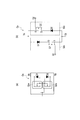
第1の実施の形態に係るFET並列回路セル10は、図3に示すように、並列接続された複数のSiC-MISFETQS1、QS2、QS3、…、QS6と、複数のSiC-MISFETQS1、QS2、QS3、…、QS6のゲートにそれぞれ接続された複数のゲートドライブ回路121、122、123、…、126と、複数のゲートドライブ回路121、122、123、…、126にゲート駆動信号を供給するOE変換器14と、複数のゲートドライブ回路121、122、123、…、126とOE変換器14に電源を供給する絶縁型DC/DC変換器16とを備える。OE変換器14には、光ファイバーケーブル18を介してON/OFF信号が供給され、一方、絶縁型DC/DC変換器16には、ゲートドライブ電圧供給線20を介して、例えば、+24VのDC電圧が供給される。SiC-MISFETQS1、QS2、QS3、…、QS6のドレインは、正側電力端子P(+)に共通接続され、SiC-MISFETQS1、QS2、QS3、…、QS6のソースは、負側電力端子N(-)に共通接続されている。
(FET並列回路セル)
第1の実施の形態に係るFET並列回路セル10は、図3に示すように、並列接続された複数のSiC-MISFETQS1、QS2、QS3、…、QS6と、複数のSiC-MISFETQS1、QS2、QS3、…、QS6のゲートにそれぞれ接続された複数のゲートドライブ回路121、122、123、…、126と、複数のゲートドライブ回路121、122、123、…、126にゲート駆動信号を供給するOE変換器14と、複数のゲートドライブ回路121、122、123、…、126とOE変換器14に電源を供給する絶縁型DC/DC変換器16とを備える。OE変換器14には、光ファイバーケーブル18を介してON/OFF信号が供給され、一方、絶縁型DC/DC変換器16には、ゲートドライブ電圧供給線20を介して、例えば、+24VのDC電圧が供給される。SiC-MISFETQS1、QS2、QS3、…、QS6のドレインは、正側電力端子P(+)に共通接続され、SiC-MISFETQS1、QS2、QS3、…、QS6のソースは、負側電力端子N(-)に共通接続されている。
OE変換器14は、光電変換素子であり、例えば、フォトカプラ、ファイバーカプラなどを適用可能である。
ここで、適用可能なSiC-MISFETQS1、QS2、QS3、…、QS6の性能としては、例えば、一般の仕様書上での定格ドレイン・ソース間電圧1200V、定格ドレインパルス電流80Aである。また、ドレイン・ソース間オン抵抗RDS(on)は、例えば、ゲート・ソース間電圧VGS=18V、ドレイン電流ID=10Aにおいて、約80mΩである。
SiC-MISFETは定格ドレイン・ソース間電圧に対するアバランシェ降伏のマージンが大きい。例えば、1200VのSiC-MISFETでは、パルス状の電圧については、1700V程度までアバランシェ降伏が起きることなく動作する。
同様に、例えば、3300VのSiC-MISFETでは、パルス状の電圧については、4000V程度までアバランシェ降伏が起きることなく動作する。
SiC-MISFETにおいて、アバランシェ降伏電圧が高く設定されている理由は以下の通りである。SiCを酸化したSiO2で形成されるゲート絶縁膜(132:図12・図13参照)を形成する過程で、炭素(C)原子の一部がSiC/SiO2界面に残留して界面準位密度を低下させる。このため、ゲート絶縁膜(SiO2)の厚膜化が難しい。一方、継続・断続的に例えば1200V耐圧デバイスに対して1700Vが掛かることはゲート絶縁膜の信頼性上避けなければならないが、異常動作時に瞬間的に掛かることに対してはゲート絶縁膜の耐量が得られる。したがって、ゲート絶縁膜に継続・断続的に掛かる電界強度を抑制することを目的としてドリフト層(126・126N:図12・図13参照)の膜厚・キャリア濃度を設計したため、SiC-MISFETは定格ドレイン・ソース間電圧に対するマージンが大きく設定されている。
(疑似高電圧FETモジュール)
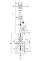
第1の実施の形態に係る疑似高電圧FETモジュール1は、図4に示すように、上記のFET並列回路セル10を複数段直列接続したスイッチング回路4と、スイッチング回路4を構成する複数のFET並列回路セル101、102、103、…、108にそれぞれ光ファイバーケーブル181、182、183、…、188を介して接続される複数のEO変換器221、222、223、…、228と、複数のEO変換器221、222、223、…、228にそれぞれ接続され、スイッチング回路4を構成する複数のFET並列回路セル101、102、103、…、108を実質的に同時にオン/オフ制御可能な複数のパルスディレー回路241、242、243、…、248とを備える。光ファイバーケーブル181、182、183、…、188は、光ファイバーケーブル束180としてバンドル化可能である。パルスディレー回路241、242、243、…、248は、例えば、FPGA(Field Programmable Gate Array)回路などで構成可能である。
第1の実施の形態に係る疑似高電圧FETモジュール1は、図4に示すように、上記のFET並列回路セル10を複数段直列接続したスイッチング回路4と、スイッチング回路4を構成する複数のFET並列回路セル101、102、103、…、108にそれぞれ光ファイバーケーブル181、182、183、…、188を介して接続される複数のEO変換器221、222、223、…、228と、複数のEO変換器221、222、223、…、228にそれぞれ接続され、スイッチング回路4を構成する複数のFET並列回路セル101、102、103、…、108を実質的に同時にオン/オフ制御可能な複数のパルスディレー回路241、242、243、…、248とを備える。光ファイバーケーブル181、182、183、…、188は、光ファイバーケーブル束180としてバンドル化可能である。パルスディレー回路241、242、243、…、248は、例えば、FPGA(Field Programmable Gate Array)回路などで構成可能である。
複数のFET並列回路セル101、102、103、…、108を複数段直列接続したスイッチング回路4は、FET並列回路セル101のドレイン側においてグローバルドレイン端子D(+)に接続され、FET並列回路セル108のソース側においてグローバルソース端子S(-)に接続される。また、パルスディレー回路241、242、243、…、248の入力側は、バッファ回路21を介して、グローバルゲート端子Gに接続される。
ここで、より一般化して、m行n列に配置するm×n個のSiC-MISFETの立ち上がり特性を測定して、立ち上がり時間が最も速いSiC-MISFETからm番目に速いSiC-MISFETまでを抽出し、最も速いSiC-MISFETからm番目に速いSiC-MISFETまでをそれぞれ異なるm個のFET並列回路セルに配置することが望ましい。スイッチング回路4を構成する複数のFET並列回路セル101、102、103、…、10mの立ち上がり時間を実質的に略均一化するためである。
第1の実施の形態においては、図3・図4に示すように、SiC-MISFETQS1、QS2、QS3、…、QS6による複数のFET並列回路セル101、102、103、…、108を直列接続して、疑似高電圧FETモジュール1を実現している。
SiC-MISFETは、Si-MISFETに比べて規格化オン抵抗が1/10以下と小さく、各FET並列回路セル101、102、103、…、108を実質的に同時にオン/オフさせるためには特別の注意、対策を行う必要がある。もしもFET並列回路セル101、102、103、…、108のスイッチングのタイミングが異なる場合には、分圧のバランスが崩れ、特定のFET並列回路セルに過大電圧が発生するからである。
第1の実施の形態においては、図4に示すように、各FET並列回路セル101、102、103、…、108毎にパルスディレー回路241、242、243、…、248を設置して、オンディレー時間とオフディレー時間を調整することによって、各FET並列回路セル101、102、103、…、108をプラスマイナス数ns以内、例えば、プラスマイナス1ns以内でオン/オフさせることができる。このため、各FET並列回路セル101、102、103、…、108を実質的に同時にオン/オフさせることができる。
ここで、第1の実施の形態において、SiC-MISFETQM1、QM2、QM3、…、QM6として、定格ドレイン・ソース間電圧1200V、定格ドレインパルス電流80AのSiC-MISFETを適用した場合、定格スイッチング電圧9.6kV、定格スイッチング電流480Aの疑似高電圧FETモジュール1を実現可能である。さらにSiCはSiと比較して200℃以上でもオフ状態が保持できるため、従来と同じ放熱システムのまま繰り返し周波数を高くすることができる。
第1の実施の形態によれば、このFET並列回路セルを複数段直列化したスイッチング回路のFET並列回路セルを実質的に同時にオン/オフ制御可能であり、FET並列回路セルの分圧バランスを良好に保持可能で、大電流をMHz級の周波数でスイッチング可能な疑似高電圧FETモジュールを提供することができる。
[第2の実施の形態]
(FET並列回路セル)
第2の実施の形態に係るFET並列回路セル10は、図5に示すように、SiC-MISFETQS1、QS2、QS3、…、QS6と並列接続され、サージ電圧を吸収するサージ吸収回路26を備える。ここで、サージ吸収回路26は、定電圧素子、アバランシェダイオード(ABD:Avalanche Breakdown Diode)などを備えていても良い。その他の構成は、第1の実施の形態に係るFET並列回路セル10と同様である。
(FET並列回路セル)
第2の実施の形態に係るFET並列回路セル10は、図5に示すように、SiC-MISFETQS1、QS2、QS3、…、QS6と並列接続され、サージ電圧を吸収するサージ吸収回路26を備える。ここで、サージ吸収回路26は、定電圧素子、アバランシェダイオード(ABD:Avalanche Breakdown Diode)などを備えていても良い。その他の構成は、第1の実施の形態に係るFET並列回路セル10と同様である。
(疑似高電圧FETモジュール)
第2の実施の形態においても、図4と同様に、SiC-MISFETQS1、QS2、QS3、…、QS6およびサージ吸収回路26を備える複数のFET並列回路セル101、102、103、…、108を直列接続して、疑似高電圧FETモジュール1を実現可能である。SiC-MISFETQS1、QS2、QS3、…、QS6として、定格ドレイン・ソース間電圧1200V、定格ドレインパルス電流80AのSiC-MISFETを適用した場合、定格スイッチング電圧9.6kV、定格スイッチング電流480Aの疑似高電圧FETモジュール1を実現可能である。
第2の実施の形態においても、図4と同様に、SiC-MISFETQS1、QS2、QS3、…、QS6およびサージ吸収回路26を備える複数のFET並列回路セル101、102、103、…、108を直列接続して、疑似高電圧FETモジュール1を実現可能である。SiC-MISFETQS1、QS2、QS3、…、QS6として、定格ドレイン・ソース間電圧1200V、定格ドレインパルス電流80AのSiC-MISFETを適用した場合、定格スイッチング電圧9.6kV、定格スイッチング電流480Aの疑似高電圧FETモジュール1を実現可能である。
SiC-MISFETは定格ドレイン・ソース間電圧に対するマージンが大きい。例えば、1200V耐圧のSiC-MISFETでは、パルス状の電圧については、1700V程度までアバランシェ降伏が起きることなく動作する。
同様に、例えば、3300VのSiC-MISFETでは、パルス状の電圧については、4000V程度までアバランシェ降伏が起きることなく動作する。
SiC-MISFETにおいて、アバランシェ降伏電圧が高く設定されている理由は前述の通りである。
第2の実施の形態に係る疑似高電圧FETモジュールにおいても各FET並列回路セル101、102、103、…、108毎にパルスディレー回路241、242、243、…、248を設置して、オンディレー時間とオフディレー時間を調整することによって、各FET並列回路セル101、102、103、…、108を実質的に略同時にオン/オフさせる回路構成とすることができる。また、第2の実施の形態においては、FET並列回路セル101、102、103、…、108に、例えば、ABD(avalanche breakdown diode)などによるサージ吸収回路26を設置することで、各並列FET回路セル101、102、103、…、108が突発的に完全に同時にオン/オフしなくても、プラスマイナス数10ns以内、例えば、プラスマイナス20ns以内でオン/オフさせることで、正常動作可能な疑似高電圧FETモジュール1を実現可能である。
サージ吸収回路26には、降伏電圧350V程度のABDを4個直列接続して、SiC-MISFETに1400Vを超える過大電圧が印加されることを回避可能である。
同様に、降伏電圧370V程度のABDを10個直列接続して、SiC-MISFETに3700Vを超える過大電圧が印加されることを回避可能である。
第2の実施の形態によれば、ABDによってアバランシェ降伏電圧以上の電圧サージを吸収可能なFET並列回路セルを提供することができる。
SiC―MISFETを使ったFET並列回路セルを構築する際、ABDを並列接続すると単位FET並列回路セル当たりが受け持てる電圧値がABDのアバランシェ降伏電圧によって規定される。このため、ABDのアバランシェ降伏電圧をSiC-MISFETの定格ドレイン・ソース間電圧以上で、かつSiC-MISFETのアバランシェ降伏電圧以下になるように設計すると良い。このように設計することで、単位FET並列回路セル当たりが受け持てる電圧値を増加させ、擬似高電圧FETモジュールに必要な電圧を確保するために直列接続するFET並列回路セルの数を低減させることができる。結果として、疑似高電圧FETモジュールの小型化、低コスト化が可能になる。
また、第2の実施の形態によれば、このFET並列回路セルを複数段直列化したスイッチング回路のFET並列回路セルを実質的に略同時にオン/オフ制御可能であり、FET並列回路セルの分圧バランスを良好に保持可能で、大電流をMHz級の周波数でスイッチング可能な疑似高電圧FETモジュールを提供することができる。
[第3の実施の形態]
(FET並列回路セル)
絶縁型DC/DC変換器16には、トランス絶縁型DC/DC変換器、或いはワイヤレス給電型の絶縁型DC/DC変換器を適用可能である。
(FET並列回路セル)
絶縁型DC/DC変換器16には、トランス絶縁型DC/DC変換器、或いはワイヤレス給電型の絶縁型DC/DC変換器を適用可能である。
トランス絶縁型DC/DC変換器28Aを適用した第3の実施の形態に係るFET並列回路セル34Aの模式的ブロック構成は、図6に示すように表される。
FET並列回路セル34Aは、トランス絶縁型DC/DC変換器28Aと、トランス絶縁型DC/DC変換器28Aに接続されたSiC-MISFET駆動回路30Aと、SiC-MISFET駆動回路30Aに接続された6並列SiC-MISFET回路32Aとを備える。トランス絶縁型DC/DC変換器28Aは、SiC-MISFET駆動回路30Aに対して直流電圧VDDを供給し、SiC-MISFET駆動回路30Aは、6並列SiC-MISFET回路32Aに対してゲート駆動信号FDを供給する。
SiC-MISFET駆動回路30Aは、図1・図3・図5に示された複数のゲートドライブ回路121、122、123、…、126に対応している。また、6並列SiC-MISFET回路32Aは、図1・図3・図5に示され、並列接続されたSiC-MISFETQS1、QS2、QS3、…、QS6に対応している。トランス絶縁型DC/DC変換器では、最大で数10kVの絶縁耐圧VBMとなる。
ワイヤレス給電型の絶縁型DC/DC変換器28を適用した第3の実施の形態に係るFET並列回路セル34の模式的ブロック構成は、図7に示すように表される。
第3の実施の形態に係るFET並列回路セル34は、図7に示すように、ワイヤレス給電型の絶縁型DC/DC変換器28と、絶縁型DC/DC変換器28に接続されたSiC-MISFET駆動回路30と、SiC-MISFET駆動回路30に接続された6並列SiC-MISFET回路32とを備える。絶縁型DC/DC変換器28は、SiC-MISFET駆動回路30に対して直流電圧VDDを供給し、SiC-MISFET駆動回路30は、6並列SiC-MISFET回路32に対してゲート駆動信号FDを供給する。
SiC-MISFET駆動回路30は、図1・図3・図5に示された複数のゲートドライブ回路121、122、123、…、126に対応している。また、6並列SiC-MISFET回路32は、図1・図3・図5に示され、並列接続されたSiC-MISFETQS1、QS2、QS3、…、QS6に対応している。
ワイヤレス給電型の絶縁型DC/DC変換器28は、図7に示すように、発振回路38と、発振回路38に接続された1次側コイルL1と、1次側コイルL1からワイヤレス給電可能な2次側コイルL2と、2次側コイルL2に接続された整流回路40とを備える。
ここで、1次側コイルL1と2次側コイルL2は、沿面距離LSだけ離隔して配置される。絶縁破壊電界の値に応じて、1次側コイルL1と2次側コイルL2間の沿面距離LSが設定される。
また、発振回路38と1次側コイルL1を内蔵し、絶縁型DC/DC変換器28の絶縁耐圧VBSを制御可能な収納器36を備えていても良い。収納器36は、樹脂もしくはセラミックスで形成されていても良い。樹脂もしくはセラミックスの厚さで絶縁耐圧値を制御することができる。例えば、ポリエチレン樹脂を使用する場合には、絶縁破壊電界は、約50kV/mmである。
ワイヤレス給電型の絶縁型DC/DC変換器28において、絶縁耐圧VBSの値は、最大数100kV以上である。
収納器36として樹脂ボックスを使用し、絶縁破壊電界1MV/8mm、約120kV/mm以上を得ることも可能である。樹脂としては、例えば、テフロン(登録商標)、ポリエチレンなどを適用可能である。
(疑似高電圧FETモジュール)
第3の実施の形態においても、第1~第2の実施の形態と同様に、複数のFET並列回路セルを直列接続して、疑似高電圧FETモジュールを実現可能である。
第3の実施の形態においても、第1~第2の実施の形態と同様に、複数のFET並列回路セルを直列接続して、疑似高電圧FETモジュールを実現可能である。
第3の実施の形態に係る疑似高電圧FETモジュールにおいては、ワイヤレス給電回路を用いて超高耐圧の絶縁型DC/DC変換器を実装することで数100kV以上の定格スイッチング電圧を有する疑似高電圧FETモジュールを実現可能である。
第3の実施の形態によれば、このFET並列回路セルを複数段直列化したスイッチング回路のFET並列回路セルを実質的に略同時にオン/オフ制御可能であり、FET並列回路セルの分圧バランスを良好に保持し、大電流をMHz級の周波数でスイッチング可能な超高耐圧用の疑似高電圧FETモジュールを提供することができる。
また、第3の実施の形態において、ABDがFET並列回路セルに接続されている場合、アバランシェ降伏電圧以上の電圧サージを吸収可能な超高耐圧のFET並列回路セルを提供することができる。
(変形例)
(FET並列回路セル)
ワイヤレス給電型の絶縁型DC/DC変換器28を適用した第3の実施の形態の変形例に係るFET並列回路セル34の模式的ブロック構成は、図8に示すように表される。
(FET並列回路セル)
ワイヤレス給電型の絶縁型DC/DC変換器28を適用した第3の実施の形態の変形例に係るFET並列回路セル34の模式的ブロック構成は、図8に示すように表される。
第3の実施の形態の変形例に係るFET並列回路セル34は、図8に示すように、ワイヤレス給電型の絶縁型DC/DC変換器28と、絶縁型DC/DC変換器28に接続されたSiC-MISFET駆動回路30と、SiC-MISFET駆動回路30に接続された6並列SiC-MISFET回路32とを備える。
SiC-MISFET駆動回路30は、図1・図3・図5に示された複数のゲートドライブ回路121、122、123、…、126に対応している。また、6並列SiC-MISFET回路32は、図1・図3・図5に示され、並列接続されたSiC-MISFETQS1、QS2、QS3、…、QS6に対応している。
絶縁型DC/DC変換器28は、SiC-MISFET駆動回路30に対して直流電圧VDDを供給し、SiC-MISFET駆動回路30は、6並列SiC-MISFET回路32に対してゲート駆動信号FDを供給する。
ワイヤレス給電型の絶縁型DC/DC変換器28は、図8に示すように、発振回路38と、発振回路38に接続された1次側コイルL1と、1次側コイルL1からワイヤレス給電可能な2次側コイルL2と、2次側コイルL2に接続された整流回路40とを備える。
さらに、第3の実施の形態の変形例に係るFET並列回路セル34は、図8に示すように、整流回路40の出力とSiC-MISFET駆動回路30の入力間に接続された蓄電回路42を備える。ここで、蓄電回路42には、リチウムイオン電池、スーパーキャパシタ、もしくは電気二重槽キャパシタ(EDLC:Electric Double-Layer Capacitor)などを適用可能である。
さらに、第3の実施の形態の変形例に係るFET並列回路セル34は、図8に示すように、整流回路40の出力に第1アノードが接続され、SiC-MISFET駆動回路30の入力に第1カソードが接続された第1突合せダイオードDT1と、蓄電回路42を介して第2アノードが整流回路40の出力に接続され、SiC-MISFET駆動回路30の入力に第2カソードが接続された第2突合せダイオードDT2とを備えていても良い。
ここで、1次側コイルL1と2次側コイルL2は、沿面距離LSだけ離隔して配置される。その他の構成は、第3の実施の形態に係るFET並列回路セル34と同様である。
(疑似高電圧FETモジュール)
第3の実施の形態の変形例に係るFET並列回路セル34は、蓄電回路42を設けることで、DC+24V電源喪失時においても各FET並列回路セルが同時にオフできるようになる。DC+24V電源喪失時においても回路内のSiC-MISFETが異常電圧によって破壊されることを回避可能であるため、信頼性の高い疑似高電圧FETモジュールを実現可能である。
第3の実施の形態の変形例に係るFET並列回路セル34は、蓄電回路42を設けることで、DC+24V電源喪失時においても各FET並列回路セルが同時にオフできるようになる。DC+24V電源喪失時においても回路内のSiC-MISFETが異常電圧によって破壊されることを回避可能であるため、信頼性の高い疑似高電圧FETモジュールを実現可能である。
第3の実施の形態の変形例に係るFET並列回路セルを適用した疑似高電圧FETモジュールにおいては、ワイヤレス給電回路を用いて超高耐圧の絶縁型DC/DC変換器を実装することで絶縁耐圧VBSとして最大数100kV以上の定格スイッチング電圧を有する疑似高電圧FETモジュールを実現可能である。
また、第3の実施の形態の変形例によれば、このFET並列回路セルを複数段直列化したスイッチング回路のFET並列回路セルを実質的に略同時にオン/オフ制御可能であり、FET並列回路セルの分圧バランスを良好に保持し、大電流をMHz級の周波数でスイッチング可能な超高耐圧用の疑似高電圧FETモジュールを提供することができる。
また、第3の実施の形態の変形例において、ABDがFET並列回路セルに接続されている場合、アバランシェ降伏電圧以上の電圧サージを吸収可能な超高耐圧のFET並列回路セルを提供することができる。
[第4の実施の形態]
(MIS型リレー回路セル)
第1~第3の実施の形態に係るFET並列回路セルを構成するSiC-MISFETは、AC負荷をスイッチング可能なバイポーラ型であっても良い。
(MIS型リレー回路セル)
第1~第3の実施の形態に係るFET並列回路セルを構成するSiC-MISFETは、AC負荷をスイッチング可能なバイポーラ型であっても良い。
第4の実施の形態に係るMIS型リレー回路セル44は、図9に示すように、並列接続された複数のSiC-MISFET AC負荷回路QA1、QA2、QA3、…、QA6と、複数のSiC-MISFET AC負荷回路QA1、QA2、QA3、…、QA6のゲートにそれぞれ接続された複数のゲートドライブ回路121、122、123、…、126と、複数のゲートドライブ回路121、122、123、…、126にゲート駆動信号を供給するOE変換器14と、複数のゲートドライブ回路121、122、123、…、126とOE変換器14に電源を供給する絶縁型DC/DC変換器16とを備える。
OE変換器14には、光ファイバーケーブル18を介してON/OFF信号が供給され、一方、絶縁型DC/DC変換器16には、ゲートドライブ電圧供給線20を介して、例えば、+24VのDC電圧が供給される。
SiC-MISFET AC負荷回路QA1、QA2、QA3、…、QA6の一方のドレインは、正側AC端子TAに共通接続され、SiC-MISFET AC負荷回路QA1、QA2、QA3、…、QA6の他方のドレインは、負側AC端子TBに共通接続されている。
また、第4の実施の形態に係るMIS型リレー回路セル44のSiC-MISFET AC負荷回路QA1、QA2、QA3、…、QA6の回路構成例は、図10(a)に示すように表され、別の回路構成例は、図10(b)に示すように表される。
例えば、図10(a)に示すように、2個のSiC-MOSFETをソース共通で直列化接続することで、AC負荷をスイッチング可能な双方向スイッチを実現可能である。
SiC-MISFET AC負荷回路QAは、図10(a)に示すように、第1のSiC-MISFETQSAと、第1のSiC-MISFETQSAと直列に接続され、第1のSiC-MISFETQSAの第1ソースと第2ソースが共通に接続され、第1のSiC-MISFETQSAの第1ゲートと第2ゲートが共通に接続された第2のSiC-MISFETQSBと、第1のSiC-MISFETQSAの主電極間に逆並列接続された第1ダイオードD1と、第2のSiC-MISFETQSBの主電極間に逆並列接続された第2ダイオードD2とを備える。SiC-MISFET AC負荷回路QAは、第1のSiC-MISFETQSAの第1ドレインと第2のSiC-MISFETQSBの第2ドレイン間のAC電流を制御可能である。2個のSiC-MOSFETQSA・QSBのゲートを共通化し、2個のSiC-MOSFETQSA・QSBを同時にオンさせる場合、AC電流は並列ダイオードD1・D2ではなく主に低オン抵抗を有するSiC-MOSFETQSA・QSBを導通する。すなわち、SiC-MISFET AC負荷回路QAは、AC端子TA・TB間のAC電流をスイッチング制御可能である。
第4の実施の形態に係るMIS型リレー回路セル44のSiC-MISFET AC負荷回路は、図10(b)に示すように、第1のSiC-MISFETQ1と第1のSiC-MISFETQ1に直列接続された第1のダイオードD1からなる第1の逆阻止型スイッチ501と、第2のSiC-MISFETQ2と第2のSiC-MISFETQ2に直列接続された第2のダイオードD2からなる第2の逆阻止型スイッチ502とを備えていても良い。この構成にすると、第1のSiC-MISFETQ1と第1のダイオードD1、および第2のSiC-MISFETQ2と第2のダイオードD2の間の電流経路の寄生インダクタンスを低減することができ、よりサージやノイズの少ない回路を形成することができる。図10(b)に示すSiC-MISFET AC負荷回路QAは、AC端子TA・TB間のAC電流をスイッチング制御可能である。
ここで、SiC-MISFET AC負荷回路QA1、QA2、QA3、…、QA6に適用可能なSiC-MISFETQSA、QSB、Q1、Q2の性能としては、例えば、定格ドレイン・ソース間電圧1200V、定格ドレインパルス電流80Aである。また、ドレイン・ソース間オン抵抗RDS(on)は、例えば、VGS=18V、ID=10Aにおいて、約80mΩである。
絶縁型DC/DC変換器16には、トランス絶縁型DC/DC変換器、或いはワイヤレス給電型の絶縁型DC/DC変換器を適用可能である。トランス絶縁型DC/DC変換器では、最大で数10kVの絶縁耐圧VBMとなる。ワイヤレス給電型の絶縁型DC/DC変換器において、絶縁耐圧VBSの値は、最大数100kV以上である。
ワイヤレス給電型の絶縁型DC/DC変換器28は、図7と同様に、発振回路38と、発振回路38に接続された1次側コイルL1と、1次側コイルL1からワイヤレス給電可能な2次側コイルL2と、2次側コイルL2に接続された整流回路40とを備える。ここで、1次側コイルL1と2次側コイルL2は、沿面距離LSだけ離隔して配置される。
また、ワイヤレス給電型の絶縁型DC/DC変換器28は、図7と同様に、発振回路38と1次側コイルL1を内蔵し、絶縁型DC/DC変換器28の絶縁耐圧VBSを制御可能な収納器36を備えていても良い。収納器36は、樹脂もしくはセラミックスで形成されていても良い。樹脂もしくはセラミックスの厚さで絶縁耐圧値を制御することができる。例えば、ポリエチレン樹脂を使用する場合には、絶縁破壊電界は、約50kV/mmである。
収納器36として樹脂ボックスを使用し、絶縁破壊電界1MV/8mm、約120kV/mm以上を得ることも可能である。樹脂としては、例えば、テフロン(登録商標)、ポリエチレンなどを適用可能である。
さらに、第4の実施の形態に係るMIS型リレー回路セル44は、図8と同様に、整流回路40の出力と複数のゲートドライブ回路121、122、123、…、126の入力間に接続された蓄電回路42を備えていても良い。ここで、蓄電回路42には、リチウムイオン電池、スーパーキャパシタ、もしくは電気二重槽キャパシタ(EDLC)などを適用可能である。
さらに、第4の実施の形態に係るMIS型リレー回路セル44は、図8と同様に、整流回路40の出力に第1アノードが接続され、SiC-MISFET駆動回路30の入力に第1カソードが接続された第1突合せダイオードDT1と、蓄電回路42を介して第2アノードが整流回路40の出力に接続され、SiC-MISFET駆動回路30の入力に第2カソードが接続された第2突合せダイオードDT2とを備えていても良い。
(疑似高電圧FETモジュール:疑似高電圧MIS型リレーモジュール)
第4の実施の形態に係る疑似高電圧FETモジュール2は、図11に示すように、上記のMIS型リレー回路セル44を複数段直列接続したスイッチング回路8と、スイッチング回路8を構成する複数のMIS型リレー回路セル441、442、443、…、448にそれぞれ光ファイバーケーブル181、182、183、…、188を介して接続される複数のEO変換器221、222、223、…、228と、複数のEO変換器221、222、223、…、228にそれぞれ接続され、スイッチング回路4を構成する複数のMIS型リレー回路セル441、442、443、…、448を同時にオン/オフ制御可能な複数のパルスディレー回路241、242、243、…、248とを備える。光ファイバーケーブル181、182、183、…、188は、光ファイバーケーブル束180としてバンドル化可能である。パルスディレー回路241、242、243、…、248は、例えば、FPGA回路などで構成可能である。
第4の実施の形態に係る疑似高電圧FETモジュール2は、図11に示すように、上記のMIS型リレー回路セル44を複数段直列接続したスイッチング回路8と、スイッチング回路8を構成する複数のMIS型リレー回路セル441、442、443、…、448にそれぞれ光ファイバーケーブル181、182、183、…、188を介して接続される複数のEO変換器221、222、223、…、228と、複数のEO変換器221、222、223、…、228にそれぞれ接続され、スイッチング回路4を構成する複数のMIS型リレー回路セル441、442、443、…、448を同時にオン/オフ制御可能な複数のパルスディレー回路241、242、243、…、248とを備える。光ファイバーケーブル181、182、183、…、188は、光ファイバーケーブル束180としてバンドル化可能である。パルスディレー回路241、242、243、…、248は、例えば、FPGA回路などで構成可能である。
複数のMIS型リレー回路セル441、442、443、…、448を複数段直列接続したスイッチング回路4は、MIS型リレー回路セル441の一方のドレイン側においてグローバルAC端子T1に接続され、MIS型リレー回路セル448の他方のドレイン側においてグローバルAC端子T2に接続される。また、パルスディレー回路241、242、243、…、248の入力側は、バッファ回路21を介して、グローバルゲート端子Gに接続される。
第4の実施の形態においては、図9~図11に示すように、SiC-MISFET AC負荷回路QA1、QA2、QA3、…、QA6による複数のMIS型リレー回路セル441、442、443、…、448を直列接続して、疑似高電圧FETモジュール2を実現している。
第4の実施の形態においては、図11に示すように、各MIS型リレー回路セル441、442、443、…、448毎にパルスディレー回路241、242、243、…、248を設置して、オンディレー時間とオフディレー時間を調整することによって、各MIS型リレー回路セル441、442、443、…、448をプラスマイナス数ns以内、例えば、プラスマイナス1ns以内でオン/オフさせることができる。このため、各MIS型リレー回路セル441、442、443、…、448を略同時にオン/オフさせることができる。
ここで、第4の実施の形態において、定格ドレイン・ソース間電圧1200V、定格ドレインパルス電流80AのSiC-MISFETを適用した場合、定格スイッチング電圧9.6kV、定格スイッチング電流480Aの疑似高電圧FETモジュール2を実現可能である。
また、第4の実施の形態の変形例によれば、このFET並列回路セルを複数段直列化したスイッチング回路のMIS型リレー回路セルを実質的に略同時にオン/オフ制御可能であり、MIS型リレー回路セルの分圧バランスを良好に保持可能な高速スイッチング性能の疑似高電圧FETモジュール(疑似高電圧MIS型リレーモジュール)を提供することができる。
また、第4の実施の形態において、ABDがFET並列回路セルに接続されている場合、アバランシェ降伏電圧以上の電圧サージを吸収可能なMIS型リレー回路セルを提供することができる。
(半導体デバイスの構成例)
―SiC DIMISFET―
第1~第4の実施の形態に係る疑似高電圧FETモジュール1・2に適用可能な半導体デバイス100の例であって、SiC DI(Double Implanted)MISFETの模式的断面構造は、図12に示すように表される。
―SiC DIMISFET―
第1~第4の実施の形態に係る疑似高電圧FETモジュール1・2に適用可能な半導体デバイス100の例であって、SiC DI(Double Implanted)MISFETの模式的断面構造は、図12に示すように表される。
第1~第4の実施の形態に係る疑似高電圧FETモジュール1・2に適用可能なSiC DIMISFETは、図12に示すように、n+SiC基板124と、n+SiC基板124上にエピタキシャル成長されたn-ドリフト層126と、n-ドリフト層126の表面側に形成されたpボディ領域128と、pボディ領域128の表面に形成されたn+ソース領域130と、pボディ領域128間のn-ドリフト層126の表面上に配置されたゲート絶縁層132と、ゲート絶縁層132上に配置されたゲート電極138と、n+ソース領域130およびpボディ領域128に電気的に接続されたソース電極134と、n+SiC基板124の、n-ドリフト層126と反対側の表面に電気的に接続されたドレイン電極136とを備える。
図12では、半導体デバイス100は、pボディ領域128と、pボディ領域128の表面に形成されたn+ソース領域130が、ダブルイオン注入(DI)で形成され、ソースパッド電極SPは、n+ソース領域130およびpボディ領域128に接続されたソース電極134に接続される。ゲートパッド電極GP(図示省略)は、ゲート絶縁層132上に配置されたゲート電極138に接続される。また、ソースパッド電極SP・ソース電極134およびゲートパッド電極GP(図示省略)は、図12に示すように、半導体デバイス100の表面を覆うパッシベーション用の層間絶縁膜144上に配置される。
―SiC TMISFET―
第1~第4の実施の形態に係る疑似高電圧FETモジュール1・2に適用可能な半導体デバイス100の例であって、SiC TMISFETの模式的断面構造は、図13に示すように表される。
第1~第4の実施の形態に係る疑似高電圧FETモジュール1・2に適用可能な半導体デバイス100の例であって、SiC TMISFETの模式的断面構造は、図13に示すように表される。
第1~第4の実施の形態に係る疑似高電圧FETモジュール1・2に適用可能なSiC TMISFETは、図13に示すように、n+SiC基板124と、n+SiC基板124上にエピタキシャル成長されたn-ドリフト層126Nと、n-ドリフト層126Nの表面側に形成されたpボディ領域128と、pボディ領域128の表面に形成されたn+ソース領域130と、pボディ領域128を貫通し、n-ドリフト層126Nまで形成されたトレンチの内にゲート絶縁層132および層間絶縁膜144U・144Bを介して形成されたトレンチゲート電極138TGと、ソース領域130およびpボディ領域128に接続されたソース電極134と、n+SiC基板124の、n-ドリフト層126Nと反対側の表面に電気的に接続されたドレイン電極136とを備える。
図13では、半導体デバイス100は、pボディ領域128を貫通し、半導体基板126Nまで形成されたトレンチ内にゲート絶縁層132および層間絶縁膜144U・144Bを介して形成されたトレンチゲート電極138TGが形成され、ソースパッド電極SPは、ソース領域130およびpボディ領域128に接続されたソース電極134に接続される。ゲートパッド電極GP(図示省略)は、ゲート層132上に配置されたゲート電極138に接続される。また、ソースパッド電極SP・ソース電極134およびゲートパッド電極GP(図示省略)は、図13に示すように、半導体デバイス100の表面を覆うパッシベーション用の層間絶縁膜144U上に配置される。
SiC-TMISFETはドレイン電流経路にpボディ領域128から伸張するジャンクション抵抗が存在しないため、SIC DMISFETと比較してさらに低オン抵抗のFETを提供することが可能であり、1素子当たりに100A以上のドレインパルス電流を許容することも可能になる。
また、第1~第4の実施の形態に係る疑似高電圧FETモジュール1・2に適用可能な半導体デバイス100には、SiC系MISFETの代わりに、GaN系FETなどを適用することもできる。
SiCデバイスは、高絶縁破壊電界(例えば、約3MV/cmであり、Siの約3倍)であることから、Siに比べてドリフト層の膜厚を薄くし、かつキャリア濃度を高く設定しても耐圧が確保できる。絶縁破壊電界の違いから、SiC-MISFETのピーク電界強度は、Si-MISFETのピーク電界強度よりも高く設定可能である。
SiC-MISFETにおいては、必要なn-ドリフト層126・126Nの膜厚が薄く、キャリア濃度と膜厚の双方のメリットによって、n-ドリフト層126・126Nの抵抗値を低減し、オン抵抗Ronを低くすることができ、チップ面積を縮小化(小チップ化)可能である。さらにユニポーラデバイスであるMISFET構造のままで、Si IGBTに比肩し得る耐圧を実現可能であることから、高耐圧でかつ高速スイッチングできるとされ、スイッチング損失の低減が期待できる。
以上説明したように、本発明によれば、SiC―MISFET並列回路セルおよびこのFET並列回路セルを複数段直列化した、大電流をMHz級の周波数でスイッチング可能な疑似高電圧FETモジュールを提供することができる。
[その他の実施の形態]
上記のように、第1~第4の実施の形態によって記載したが、この開示の一部をなす論述および図面は例示的なものであり、この発明を限定するものであると理解すべきではない。この開示から当業者には様々な代替実施の形態、実施例および運用技術が明らかとなろう。
上記のように、第1~第4の実施の形態によって記載したが、この開示の一部をなす論述および図面は例示的なものであり、この発明を限定するものであると理解すべきではない。この開示から当業者には様々な代替実施の形態、実施例および運用技術が明らかとなろう。
また、FETの高速化動作、もしくは誤動作回避を目的として、ゲートオフ時のゲート・ソース間電圧を負電圧側に引いても良い。
このように、本発明はここでは記載していない様々な実施の形態などを含む。
本発明のFET並列回路セルおよび疑似高電圧FETモジュールは、パワーSiC-MISFETを用いた高電圧高速スイッチを有するパルスパワー発生装置、高繰り返し高電圧パルスパワー発生装置など幅広い応用分野に適用可能である。
1、1A、2…疑似高電圧FETモジュール
4、8…スイッチング回路
10、101、102、103、…、108、34、34A…FET並列回路セル
12、121、122、123、…、126…ゲートドライブ回路
14…OE変換器
16、28、28A…絶縁型DC/DC変換器
18、181、182、183、…、188…光ファイバーケーブル
20…ゲートドライブ電圧供給線
21…バッファ回路
22、221、222、223、…、226…EO変換器
241、242、243、…、246…パルスディレー回路
26…サージ吸収回路
30、30A…SiC-MISFET駆動回路
32、32A…6並列SiC-MISFET回路
36…樹脂ボックス
38…発振回路
40…整流回路
44、441、442、443、…、446…MIS型リレー回路セル
501、502…逆阻止型スイッチ
100、QSA、QSB、Q1、Q2…半導体デバイス(SiC-MISFET)
124…n+SiC基板
126、126N…n-ドリフト層
128…pボディ領域
130…ソース領域
132…ゲート絶縁膜
134…ソース電極
136…ドレイン電極
138、138TG…ゲート電極
144、144U、144B…層間絶縁膜
180、180A…光ファイバーケーブル束
QS1、QS2、QS3、…、QS6…SiC-MISFET
QM1、QM2、QM3、…、QM6…Si-MISFET
QA1、QA2、QA3、…、QA6…SiC-MISFET AC負荷回路
G…グローバルゲート端子
D(+)…グローバルドレイン端子
S(-)…グローバルソース端子
DT1、DT2…突合せダイオード
D1、D2…ダイオード
P(+)…正側電力端子
N(-)…負側電力端子
TA、TB・・・AC端子
T1、T2・・・グローバルAC端子
L1…1次側コイル
L2…2次側コイル
LS…沿面距離
4、8…スイッチング回路
10、101、102、103、…、108、34、34A…FET並列回路セル
12、121、122、123、…、126…ゲートドライブ回路
14…OE変換器
16、28、28A…絶縁型DC/DC変換器
18、181、182、183、…、188…光ファイバーケーブル
20…ゲートドライブ電圧供給線
21…バッファ回路
22、221、222、223、…、226…EO変換器
241、242、243、…、246…パルスディレー回路
26…サージ吸収回路
30、30A…SiC-MISFET駆動回路
32、32A…6並列SiC-MISFET回路
36…樹脂ボックス
38…発振回路
40…整流回路
44、441、442、443、…、446…MIS型リレー回路セル
501、502…逆阻止型スイッチ
100、QSA、QSB、Q1、Q2…半導体デバイス(SiC-MISFET)
124…n+SiC基板
126、126N…n-ドリフト層
128…pボディ領域
130…ソース領域
132…ゲート絶縁膜
134…ソース電極
136…ドレイン電極
138、138TG…ゲート電極
144、144U、144B…層間絶縁膜
180、180A…光ファイバーケーブル束
QS1、QS2、QS3、…、QS6…SiC-MISFET
QM1、QM2、QM3、…、QM6…Si-MISFET
QA1、QA2、QA3、…、QA6…SiC-MISFET AC負荷回路
G…グローバルゲート端子
D(+)…グローバルドレイン端子
S(-)…グローバルソース端子
DT1、DT2…突合せダイオード
D1、D2…ダイオード
P(+)…正側電力端子
N(-)…負側電力端子
TA、TB・・・AC端子
T1、T2・・・グローバルAC端子
L1…1次側コイル
L2…2次側コイル
LS…沿面距離
Claims (17)
- 並列接続された複数のSiC-MISFETと、
複数の前記SiC-MISFETのゲートにそれぞれ接続された複数のゲートドライブ回路と、
複数の前記ゲートドライブ回路にゲート駆動信号を供給するOE変換器と、
複数の前記ゲートドライブ回路と前記OE変換器に電源を供給する絶縁型DC/DC変換器と
を備えることを特徴とするFET並列回路セル。 - 前記SiC-MISFETと並列接続され、サージ電圧を吸収するサージ吸収回路を備えることを特徴とする請求項1に記載のFET並列回路セル。
- 前記絶縁型DC/DC変換器は、
発振回路と、
前記発振回路に接続された1次側コイルと、
前記1次側コイルと沿面距離離隔して配置され、前記1次側コイルからワイヤレス給電可能な2次側コイルと、
前記2次側コイルに接続された整流回路と
を備える
ることを特徴とする請求項1または2に記載のFET並列回路セル。 - 前記整流回路の出力と前記ゲートドライブ回路の入力間に接続された蓄電回路と、
前記整流回路の出力に第1アノードが接続され、前記ゲートドライブ回路の入力に第1カソードが接続された第1突合せダイオードと、
前記蓄電回路を介して第2アノードが前記整流回路の出力に接続され、前記ゲートドライブ回路の入力に第2カソードが接続された第2突合せダイオードと
を備えることを特徴とする請求項3に記載のFET並列回路セル。 - 前記蓄電回路は、リチウムイオン電池、スーパーキャパシタ、もしくは電気二重槽キャパシタのいずれかを備えることを特徴とする請求項4に記載のFET並列回路セル。
- 前記発振回路と前記1次側コイルを内蔵し、前記絶縁型DC/DC変換器の絶縁耐圧を制御可能な収納器を備えることを特徴とする請求項3~5のいずれか1項に記載のFET並列回路セル。
- 前記収納器は、樹脂もしくはセラミックスで形成されていることを特徴とする請求項6に記載のFET並列回路セル。
- 請求項1~7のいずれか1項に記載のFET並列回路セルを複数段直列接続したスイッチング回路と、
前記スイッチング回路を構成する複数の前記FET並列回路セルにそれぞれに光ファイバーケーブルを介して接続される複数のEO変換器と、
複数の前記EO変換器にそれぞれ接続され、前記スイッチング回路を構成する複数の前記FET並列回路セルを実質的に同時にオン/オフ制御可能な複数のパルスディレー回路と
を備えることを特徴とする疑似高電圧FETモジュール。 - m行n列に配置するm×n個のSiC-MISFETの立ち上がり特性を測定して、立ち上がり時間が最も速いSiC-MISFETからm番目に速いSiC-MISFETまでを抽出し、最も速いSiC-MISFETからm番目に速いSiC-MISFETまでをそれぞれ異なるm個のFET並列回路セルに配置することを特徴とする請求項8に記載の疑似高電圧FETモジュール。
- 並列接続された複数のSiC-MISFET AC負荷回路と、
複数の前記SiC-MISFET AC負荷回路のゲートにそれぞれ接続された複数のゲートドライブ回路と、
複数の前記ゲートドライブ回路にゲート駆動信号を供給するOE変換器と、
複数の前記ゲートドライブ回路と前記OE変換器に電源を供給する絶縁型DC/DC変換器と
を備えることを特徴とするMIS型リレー回路セル。 - 前記SiC-MISFET AC負荷回路は、
第1のSiC-MISFETと、
前記第1のSiC-MISFETと直列に接続され、前記第1のSiC-MISFETの第1ソースと第2ソースが接続され、前記第1のSiC-MISFETの第1ゲートと第2ゲートが共通に接続された第2のSiC-MISFETと、
前記第1のSiC-MISFETの主電極間に逆並列接続された第1ダイオードと、
前記第2のSiC-MISFETの主電極間に逆並列接続された第2ダイオードと
を備え、
前記第1のSiC-MISFETの第1ドレインと前記第2のSiC-MISFETの第2ドレイン間のAC電流を制御可能であることを特徴とする請求項10に記載のMIS型リレー回路セル。 - 前記絶縁型DC/DC変換器は、
発振回路と、
前記発振回路に接続された1次側コイルと、
前記1次側コイルと沿面距離離隔して配置され、前記1次側コイルからワイヤレス給電可能な2次側コイルと、
前記2次側コイルに接続された整流回路と
を備える
ることを特徴とする請求項10または11に記載のMIS型リレー回路セル。 - 前記整流回路の出力と前記ゲートドライブ回路の入力間に接続された蓄電回路と、
前記整流回路の出力に第1アノードが接続され、前記ゲートドライブ回路の入力に第1カソードが接続された第1突合せダイオードと、
前記蓄電回路を介して第2アノードが前記整流回路の出力に接続され、前記ゲートドライブ回路の入力に第2カソードが接続された第2突合せダイオードと
を備えることを特徴とする請求項12に記載のMIS型リレー回路セル。 - 前記蓄電回路は、リチウムイオン電池、スーパーキャパシタ、もしくは電気二重槽キャパシタのいずれかを備えることを特徴とする請求項13に記載のMIS型リレー回路セル。
- 前記発振回路と前記1次側コイルを内蔵し、前記絶縁型DC/DC変換器の絶縁耐圧を制御可能な収納器を備えることを特徴とする請求項12~14のいずれか1項に記載のMIS型リレー回路セル。
- 前記収納器は、樹脂もしくはセラミックスで形成されていることを特徴とする請求項15に記載のMIS型リレー回路セル。
- 請求項10~16のいずれか1項に記載のMIS型リレー回路セルを複数段直列接続したスイッチング回路と、
前記スイッチング回路を構成する複数の前記MIS型リレー回路セルにそれぞれに光ファイバーケーブルを介して接続される複数のEO変換器と、
複数の前記EO変換器にそれぞれ接続され、前記スイッチング回路を構成する複数の前記MIS型リレー回路セルを実質的に同時にオン/オフ制御可能な複数のパルスディレー回路と
を備えることを特徴とする疑似高電圧FETモジュール。
Applications Claiming Priority (2)
| Application Number | Priority Date | Filing Date | Title |
|---|---|---|---|
| JP2014038129A JP6461476B2 (ja) | 2014-02-28 | 2014-02-28 | Fet並列回路セルおよび疑似高電圧fetモジュール |
| JP2014-038129 | 2014-02-28 |
Publications (1)
| Publication Number | Publication Date |
|---|---|
| WO2015129717A1 true WO2015129717A1 (ja) | 2015-09-03 |
Family
ID=54009034
Family Applications (1)
| Application Number | Title | Priority Date | Filing Date |
|---|---|---|---|
| PCT/JP2015/055324 Ceased WO2015129717A1 (ja) | 2014-02-28 | 2015-02-25 | Fet並列回路セルおよび疑似高電圧fetモジュール |
Country Status (2)
| Country | Link |
|---|---|
| JP (1) | JP6461476B2 (ja) |
| WO (1) | WO2015129717A1 (ja) |
Cited By (2)
| Publication number | Priority date | Publication date | Assignee | Title |
|---|---|---|---|---|
| JP2017175602A (ja) * | 2016-01-29 | 2017-09-28 | トヨタ モーター エンジニアリング アンド マニュファクチャリング ノース アメリカ,インコーポレイティド | 電流/電力平衡化のための方法および装置 |
| EP3613132A1 (en) * | 2017-04-28 | 2020-02-26 | ABB Schweiz AG | Power module based on normally-on semiconductor switches |
Families Citing this family (6)
| Publication number | Priority date | Publication date | Assignee | Title |
|---|---|---|---|---|
| JP6605491B2 (ja) * | 2014-11-05 | 2019-11-13 | ローム株式会社 | 双方向acスイッチ |
| JP6418113B2 (ja) * | 2015-09-09 | 2018-11-07 | 株式会社デンソー | 駆動回路制御装置 |
| US10944392B2 (en) * | 2015-11-17 | 2021-03-09 | Autonetworks Technologies, Ltd. | Switch circuit and power supply system |
| KR102745458B1 (ko) * | 2017-09-07 | 2024-12-20 | 비식 테크놀로지스 엘티디. | 고전압 고속 스위칭 장치 |
| WO2024105880A1 (ja) * | 2022-11-18 | 2024-05-23 | 東芝三菱電機産業システム株式会社 | 駆動装置、電力変換器及び駆動方法 |
| CN120090440B (zh) * | 2024-09-30 | 2025-11-21 | 西安交通大学 | 一种适用于超高电压的全光纤隔离SiC MOSFET栅极驱动器及应用 |
Citations (4)
| Publication number | Priority date | Publication date | Assignee | Title |
|---|---|---|---|---|
| JP2000040951A (ja) * | 1998-05-18 | 2000-02-08 | Toshiba Corp | 半導体素子、その駆動方法及び駆動装置 |
| JP2006042563A (ja) * | 2004-07-30 | 2006-02-09 | Tokyo Electric Power Co Inc:The | 電力スイッチング回路、電力変換装置、開放故障検出方法及びモジュール型半導体スイッチング素子の駆動方法 |
| JP2008244972A (ja) * | 2007-03-28 | 2008-10-09 | Advantest Corp | 半導体リレー |
| JP2009135626A (ja) * | 2007-11-29 | 2009-06-18 | Mitsubishi Electric Corp | 並列駆動装置 |
Family Cites Families (1)
| Publication number | Priority date | Publication date | Assignee | Title |
|---|---|---|---|---|
| JPS6216547U (ja) * | 1985-03-29 | 1987-01-31 |
-
2014
- 2014-02-28 JP JP2014038129A patent/JP6461476B2/ja active Active
-
2015
- 2015-02-25 WO PCT/JP2015/055324 patent/WO2015129717A1/ja not_active Ceased
Patent Citations (4)
| Publication number | Priority date | Publication date | Assignee | Title |
|---|---|---|---|---|
| JP2000040951A (ja) * | 1998-05-18 | 2000-02-08 | Toshiba Corp | 半導体素子、その駆動方法及び駆動装置 |
| JP2006042563A (ja) * | 2004-07-30 | 2006-02-09 | Tokyo Electric Power Co Inc:The | 電力スイッチング回路、電力変換装置、開放故障検出方法及びモジュール型半導体スイッチング素子の駆動方法 |
| JP2008244972A (ja) * | 2007-03-28 | 2008-10-09 | Advantest Corp | 半導体リレー |
| JP2009135626A (ja) * | 2007-11-29 | 2009-06-18 | Mitsubishi Electric Corp | 並列駆動装置 |
Cited By (2)
| Publication number | Priority date | Publication date | Assignee | Title |
|---|---|---|---|---|
| JP2017175602A (ja) * | 2016-01-29 | 2017-09-28 | トヨタ モーター エンジニアリング アンド マニュファクチャリング ノース アメリカ,インコーポレイティド | 電流/電力平衡化のための方法および装置 |
| EP3613132A1 (en) * | 2017-04-28 | 2020-02-26 | ABB Schweiz AG | Power module based on normally-on semiconductor switches |
Also Published As
| Publication number | Publication date |
|---|---|
| JP6461476B2 (ja) | 2019-01-30 |
| JP2015162845A (ja) | 2015-09-07 |
Similar Documents
| Publication | Publication Date | Title |
|---|---|---|
| JP6461476B2 (ja) | Fet並列回路セルおよび疑似高電圧fetモジュール | |
| US9130570B2 (en) | Four quadrant bidirectional switch | |
| Sabri et al. | New generation 6.5 kV SiC power MOSFET | |
| Wang et al. | Overview of silicon carbide technology: Device, converter, system, and application | |
| US9911731B2 (en) | Operational gallium nitride devices | |
| US8742628B2 (en) | Solid state circuit breaker | |
| US20150108958A1 (en) | Hybrid three-level t-type converter for power applications | |
| US9214459B2 (en) | Semiconductor device | |
| TW201143017A (en) | Electronic devices and components for high efficiency power circuits | |
| KR20170035959A (ko) | 변압기를 갖는 dc-dc 컨버터 및 dc-dc 컨버터를 갖는 dc 네트워크 및 dc 네트워크를 동작시키는 방법 | |
| JPWO2016067835A1 (ja) | パワーモジュールおよびパワー回路 | |
| US10804393B1 (en) | Monolithically-integrated AC switch having JBSFETs therein with commonly-connected drain and cathode electrodes | |
| Ishigaki et al. | A new optically-isolated power converter for 12 V gate drive power supplies applied to high voltage and high speed switching devices | |
| KR20150064603A (ko) | 반도체 소자 및 그 제조방법 | |
| Fursin et al. | 7.5 kV 4H-SiC GTO's for power conversion | |
| Tominaga et al. | Investigation on the effect of total loss reduction of HV power module by using SiC-MOSFET embedding SBD | |
| US11750109B2 (en) | Power conversion device | |
| CN108173431B (zh) | 基于同步导通技术的高压直流取能变换器 | |
| Li et al. | Design and optimization of high performance gate driver for medium-voltage SiC power modules | |
| JP2020099039A (ja) | 双方向スイッチ | |
| Hsia et al. | First Demonstration of a Fully-Vertical GaN Power finFET with Direct Optical Triggering | |
| US10651845B2 (en) | Inverter branch driver | |
| JP2006166655A (ja) | 半導体装置 | |
| KR102114717B1 (ko) | SiC 인버터 장치 | |
| Shi et al. | Investigation on the device geometry-dependent reverse recovery characteristic of AlGaN/GaN lateral field-effect rectifier (L-FER) |
Legal Events
| Date | Code | Title | Description |
|---|---|---|---|
| 121 | Ep: the epo has been informed by wipo that ep was designated in this application |
Ref document number: 15754468 Country of ref document: EP Kind code of ref document: A1 |
|
| NENP | Non-entry into the national phase |
Ref country code: DE |
|
| 122 | Ep: pct application non-entry in european phase |
Ref document number: 15754468 Country of ref document: EP Kind code of ref document: A1 |