WO2015129546A1 - 電磁波シールドフィルム、フレキシブルプリント基板、電子部品搭載基板、及び電子部品の被覆方法 - Google Patents
電磁波シールドフィルム、フレキシブルプリント基板、電子部品搭載基板、及び電子部品の被覆方法 Download PDFInfo
- Publication number
- WO2015129546A1 WO2015129546A1 PCT/JP2015/054654 JP2015054654W WO2015129546A1 WO 2015129546 A1 WO2015129546 A1 WO 2015129546A1 JP 2015054654 W JP2015054654 W JP 2015054654W WO 2015129546 A1 WO2015129546 A1 WO 2015129546A1
- Authority
- WO
- WIPO (PCT)
- Prior art keywords
- electromagnetic wave
- layer
- wave shielding
- shielding film
- film
- Prior art date
- Legal status (The legal status is an assumption and is not a legal conclusion. Google has not performed a legal analysis and makes no representation as to the accuracy of the status listed.)
- Ceased
Links
Images







Classifications
-
- B—PERFORMING OPERATIONS; TRANSPORTING
- B32—LAYERED PRODUCTS
- B32B—LAYERED PRODUCTS, i.e. PRODUCTS BUILT-UP OF STRATA OF FLAT OR NON-FLAT, e.g. CELLULAR OR HONEYCOMB, FORM
- B32B7/00—Layered products characterised by the relation between layers; Layered products characterised by the relative orientation of features between layers, or by the relative values of a measurable parameter between layers, i.e. products comprising layers having different physical, chemical or physicochemical properties; Layered products characterised by the interconnection of layers
- B32B7/02—Physical, chemical or physicochemical properties
-
- B—PERFORMING OPERATIONS; TRANSPORTING
- B32—LAYERED PRODUCTS
- B32B—LAYERED PRODUCTS, i.e. PRODUCTS BUILT-UP OF STRATA OF FLAT OR NON-FLAT, e.g. CELLULAR OR HONEYCOMB, FORM
- B32B27/00—Layered products comprising a layer of synthetic resin
- B32B27/06—Layered products comprising a layer of synthetic resin as the main or only constituent of a layer, which is next to another layer of the same or of a different material
-
- B—PERFORMING OPERATIONS; TRANSPORTING
- B32—LAYERED PRODUCTS
- B32B—LAYERED PRODUCTS, i.e. PRODUCTS BUILT-UP OF STRATA OF FLAT OR NON-FLAT, e.g. CELLULAR OR HONEYCOMB, FORM
- B32B27/00—Layered products comprising a layer of synthetic resin
- B32B27/06—Layered products comprising a layer of synthetic resin as the main or only constituent of a layer, which is next to another layer of the same or of a different material
- B32B27/08—Layered products comprising a layer of synthetic resin as the main or only constituent of a layer, which is next to another layer of the same or of a different material of synthetic resin
-
- B—PERFORMING OPERATIONS; TRANSPORTING
- B32—LAYERED PRODUCTS
- B32B—LAYERED PRODUCTS, i.e. PRODUCTS BUILT-UP OF STRATA OF FLAT OR NON-FLAT, e.g. CELLULAR OR HONEYCOMB, FORM
- B32B27/00—Layered products comprising a layer of synthetic resin
- B32B27/36—Layered products comprising a layer of synthetic resin comprising polyesters
-
- B—PERFORMING OPERATIONS; TRANSPORTING
- B32—LAYERED PRODUCTS
- B32B—LAYERED PRODUCTS, i.e. PRODUCTS BUILT-UP OF STRATA OF FLAT OR NON-FLAT, e.g. CELLULAR OR HONEYCOMB, FORM
- B32B7/00—Layered products characterised by the relation between layers; Layered products characterised by the relative orientation of features between layers, or by the relative values of a measurable parameter between layers, i.e. products comprising layers having different physical, chemical or physicochemical properties; Layered products characterised by the interconnection of layers
-
- B—PERFORMING OPERATIONS; TRANSPORTING
- B32—LAYERED PRODUCTS
- B32B—LAYERED PRODUCTS, i.e. PRODUCTS BUILT-UP OF STRATA OF FLAT OR NON-FLAT, e.g. CELLULAR OR HONEYCOMB, FORM
- B32B7/00—Layered products characterised by the relation between layers; Layered products characterised by the relative orientation of features between layers, or by the relative values of a measurable parameter between layers, i.e. products comprising layers having different physical, chemical or physicochemical properties; Layered products characterised by the interconnection of layers
- B32B7/04—Interconnection of layers
- B32B7/12—Interconnection of layers using interposed adhesives or interposed materials with bonding properties
-
- H—ELECTRICITY
- H05—ELECTRIC TECHNIQUES NOT OTHERWISE PROVIDED FOR
- H05K—PRINTED CIRCUITS; CASINGS OR CONSTRUCTIONAL DETAILS OF ELECTRIC APPARATUS; MANUFACTURE OF ASSEMBLAGES OF ELECTRICAL COMPONENTS
- H05K9/00—Screening of apparatus or components against electric or magnetic fields
- H05K9/0073—Shielding materials
- H05K9/0081—Electromagnetic shielding materials, e.g. EMI, RFI shielding
- H05K9/0083—Electromagnetic shielding materials, e.g. EMI, RFI shielding comprising electro-conductive non-fibrous particles embedded in an electrically insulating supporting structure, e.g. powder, flakes, whiskers
-
- B—PERFORMING OPERATIONS; TRANSPORTING
- B32—LAYERED PRODUCTS
- B32B—LAYERED PRODUCTS, i.e. PRODUCTS BUILT-UP OF STRATA OF FLAT OR NON-FLAT, e.g. CELLULAR OR HONEYCOMB, FORM
- B32B2307/00—Properties of the layers or laminate
- B32B2307/20—Properties of the layers or laminate having particular electrical or magnetic properties, e.g. piezoelectric
-
- B—PERFORMING OPERATIONS; TRANSPORTING
- B32—LAYERED PRODUCTS
- B32B—LAYERED PRODUCTS, i.e. PRODUCTS BUILT-UP OF STRATA OF FLAT OR NON-FLAT, e.g. CELLULAR OR HONEYCOMB, FORM
- B32B2307/00—Properties of the layers or laminate
- B32B2307/20—Properties of the layers or laminate having particular electrical or magnetic properties, e.g. piezoelectric
- B32B2307/212—Electromagnetic interference shielding
-
- B—PERFORMING OPERATIONS; TRANSPORTING
- B32—LAYERED PRODUCTS
- B32B—LAYERED PRODUCTS, i.e. PRODUCTS BUILT-UP OF STRATA OF FLAT OR NON-FLAT, e.g. CELLULAR OR HONEYCOMB, FORM
- B32B2307/00—Properties of the layers or laminate
- B32B2307/70—Other properties
- B32B2307/732—Dimensional properties
- B32B2307/734—Dimensional stability
-
- B—PERFORMING OPERATIONS; TRANSPORTING
- B32—LAYERED PRODUCTS
- B32B—LAYERED PRODUCTS, i.e. PRODUCTS BUILT-UP OF STRATA OF FLAT OR NON-FLAT, e.g. CELLULAR OR HONEYCOMB, FORM
- B32B2457/00—Electrical equipment
-
- B—PERFORMING OPERATIONS; TRANSPORTING
- B32—LAYERED PRODUCTS
- B32B—LAYERED PRODUCTS, i.e. PRODUCTS BUILT-UP OF STRATA OF FLAT OR NON-FLAT, e.g. CELLULAR OR HONEYCOMB, FORM
- B32B2457/00—Electrical equipment
- B32B2457/08—PCBs, i.e. printed circuit boards
-
- B—PERFORMING OPERATIONS; TRANSPORTING
- B32—LAYERED PRODUCTS
- B32B—LAYERED PRODUCTS, i.e. PRODUCTS BUILT-UP OF STRATA OF FLAT OR NON-FLAT, e.g. CELLULAR OR HONEYCOMB, FORM
- B32B2571/00—Protective equipment
-
- H—ELECTRICITY
- H05—ELECTRIC TECHNIQUES NOT OTHERWISE PROVIDED FOR
- H05K—PRINTED CIRCUITS; CASINGS OR CONSTRUCTIONAL DETAILS OF ELECTRIC APPARATUS; MANUFACTURE OF ASSEMBLAGES OF ELECTRICAL COMPONENTS
- H05K1/00—Printed circuits
- H05K1/02—Details
- H05K1/0213—Electrical arrangements not otherwise provided for
- H05K1/0216—Reduction of cross-talk, noise or electromagnetic interference
-
- H—ELECTRICITY
- H05—ELECTRIC TECHNIQUES NOT OTHERWISE PROVIDED FOR
- H05K—PRINTED CIRCUITS; CASINGS OR CONSTRUCTIONAL DETAILS OF ELECTRIC APPARATUS; MANUFACTURE OF ASSEMBLAGES OF ELECTRICAL COMPONENTS
- H05K1/00—Printed circuits
- H05K1/18—Printed circuits structurally associated with non-printed electric components
- H05K1/189—Printed circuits structurally associated with non-printed electric components characterised by the use of flexible or folded printed circuits
-
- H—ELECTRICITY
- H05—ELECTRIC TECHNIQUES NOT OTHERWISE PROVIDED FOR
- H05K—PRINTED CIRCUITS; CASINGS OR CONSTRUCTIONAL DETAILS OF ELECTRIC APPARATUS; MANUFACTURE OF ASSEMBLAGES OF ELECTRICAL COMPONENTS
- H05K2201/00—Indexing scheme relating to printed circuits covered by H05K1/00
- H05K2201/07—Electric details
- H05K2201/0707—Shielding
- H05K2201/0715—Shielding provided by an outer layer of PCB
Definitions
- the present invention relates to an electromagnetic wave shielding film (hereinafter also referred to as an electromagnetic wave shielding film), a flexible printed circuit board, an electronic component mounting substrate, and an electronic component coating method. More specifically, the present invention relates to an electromagnetic wave shielding film in which no crack is generated even when Z-folding is performed, and a flexible printed board using the electromagnetic wave shielding film.
- This application is filed in Japanese Patent Application No. 2014-33732 filed in Japan on February 25, 2014, Japanese Patent Application No. 2014-108082 filed in Japan on May 26, 2014, and in Japan on September 10, 2014. Claim priority based on Japanese Patent Application No. 2014-184019 filed and Japanese Patent Application No. 2014-187193 filed in Japan on September 16, 2014, the contents of which are incorporated herein by reference.
- the mounted electronic device has an electromagnetic wave shielding film attached to the surface in order to reduce the influence of noise caused by electromagnetic waves.
- an electromagnetic wave shielding film a film having a base material layer made of an insulating material and a metal layer laminated on one or both surfaces of the base material layer as described in Patent Documents 1 to 4. Have been used.
- JP 2006-156946 A Japanese Patent Application Laid-Open No. 07-297592 Japanese Patent Laid-Open No. 06-224589 Japanese Patent Laid-Open No. 06-152182
- the present invention can cope with the weight reduction and thinning of electronic parts such as flexible printed circuit boards, has excellent resistance to goby folds, and has excellent shape followability and adhesion even when affixed to the surface of uneven electronic parts. It is an object to provide an electromagnetic wave shielding film and a flexible printed circuit board.
- the object of the present invention is to reduce the weight and thickness, and to use an electromagnetic wave shielding film capable of effectively blocking electromagnetic waves in a high frequency band as in the GHz order, and the electromagnetic wave shielding film.
- An object of the present invention is to provide an electronic component mounting substrate in which an electronic component mounted on a substrate is covered with an electromagnetic wave shielding layer.
- the object of the present invention is to increase the degree of freedom in designing the substrate, reduce the weight and reduce the thickness, and for an electronic component having a substrate with unevenness, an electromagnetic shielding film having good shape followability, Another object of the present invention is to provide a method for coating an electronic component using the electromagnetic wave shielding film.
- Another object of the present invention is to increase the degree of freedom in designing the substrate and reduce the thickness, and between the electronic component having conductivity on the surface and the electromagnetic wave shielding layer with respect to the electronic component having the substrate with unevenness.
- An object of the present invention is to provide a method of coating without conducting current.
- the present inventors have conducted intensive studies to solve the above problems. As a result, at least a base material layer and an electromagnetic wave shielding layer are laminated in order, and the electromagnetic wave shielding layer is an electromagnetic wave shielding film formed from a composition having conductivity between both ends when Z-folding is performed. Found that the problem can be solved. As a result of further studies based on these findings, the present invention has been completed.
- the present invention includes the following aspects.
- the base material layer includes a laminate in which at least two layers are laminated.
- the base material layer is a laminate in which a first layer, a second layer, and a third layer are sequentially laminated, and any one of [1] to [5] The electromagnetic wave shielding film of item.
- the thickness T (A) of the first layer, the thickness T (C) of the second layer, and the thickness T (B) of the third layer satisfy the following formula (1):
- a substrate on which an electronic component is mounted comprising the electromagnetic wave shielding film according to any one of [1] to [8] as an uneven covering member on the substrate, wherein the unevenness has a step of 1 mm or more.
- a substrate comprising: [10] A flexible printed board comprising the electromagnetic wave shielding film according to any one of [1] to [8] as an electromagnetic wave shielding member.
- the film for electromagnetic wave shielding according to [11] wherein the conductive polymer is polyaniline.
- An electronic component mounting substrate having an electromagnetic wave shielding layer, The electronic component mounting substrate, wherein the electromagnetic wave shielding layer contains a conductive polymer and metal powder.
- An electromagnetic wave shielding film used for covering unevenness on a substrate, An insulating layer and an electromagnetic wave shielding layer laminated on one surface side of the insulating layer; The film for electromagnetic wave shielding, wherein the film has a thickness of 8 ⁇ m or more and 50 ⁇ m or less.
- the conductive polymer is at least one of polyethylene dioxythiophene / polystyrene sulfonate [PEDOT / PSS] and polyaniline.
- the electromagnetic wave shielding film of the present invention can cope with the reduction in weight and thickness of electronic components, has excellent resistance to goby folding, and has excellent shape followability and adhesion even when applied to the surface of an electronic component having irregularities. . Moreover, since the electromagnetic wave shielding film of the present invention is used as an electromagnetic wave shielding layer on the surface of the flexible printed board of the present invention, it can cope with the reduction in weight and thickness of electronic parts, has excellent goby folding resistance, and has unevenness. Excellent adhesion between the surface of the flexible printed circuit board and the electromagnetic shielding layer.
- the electromagnetic wave shielding film comprises a base material layer and an electromagnetic wave shielding layer containing a conductive polymer and metal powder as main materials, thereby reducing the weight of the electromagnetic wave shielding layer.
- -It can be thinned and can effectively block electromagnetic waves in a high frequency band as in the GHz order.
- the thickness of the electromagnetic wave shielding film is set to 8 ⁇ m or more and 50 ⁇ m or less, so that the degree of freedom in designing the substrate covered with the electromagnetic wave shielding film can be increased, and the weight and thickness can be reduced.
- substrate covered with the film for electromagnetic wave shielding by setting the puncture intensity
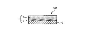
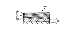
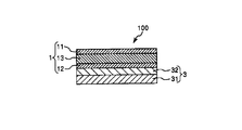
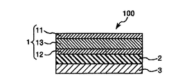
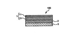
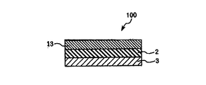
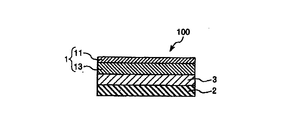
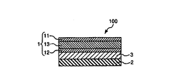
- FIG. 1 is a longitudinal cross-sectional view which shows 1st Embodiment of the electromagnetic wave shield film of this invention. It is a longitudinal cross-sectional view which shows 2nd Embodiment of the electromagnetic wave shield film of this invention. It is a longitudinal cross-sectional view which shows 3rd Embodiment of the electromagnetic wave shield film of this invention. It is a longitudinal cross-sectional view which shows 4th Embodiment of the electromagnetic wave shield film of this invention. It is a longitudinal cross-sectional view which shows 5th Embodiment of the electromagnetic wave shield film of this invention. It is a longitudinal cross-sectional view which shows 6th Embodiment of the electromagnetic wave shield film of this invention.
- FIG. 1 ist Embodiment of the electromagnetic wave shield film of this invention. It is a longitudinal cross-sectional view which shows 2nd Embodiment of the electromagnetic wave shield film of this invention. It is a longitudinal cross-sectional view which shows 3rd Embodiment of the electromagnetic wave shield film of this invention. It is a
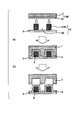
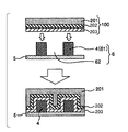
- FIG. 7 is a longitudinal sectional view for explaining a method of coating an electronic component using the electromagnetic wave shielding film shown in FIGS. It is a longitudinal cross-sectional view which shows 7th Embodiment of the film for electromagnetic wave shields of this invention. It is a longitudinal cross-sectional view for demonstrating the coating method of an electronic component using the film for electromagnetic wave shields shown in FIG. It is a longitudinal cross-sectional view which shows 8th Embodiment of the film for electromagnetic wave shields of this invention. It is a longitudinal cross-sectional view which shows 9th Embodiment of the film for electromagnetic wave shields of this invention. It is a longitudinal cross-sectional view which shows 10th Embodiment of the film for electromagnetic wave shields of this invention.
- the electromagnetic wave shielding film of this embodiment is formed by sequentially laminating at least a base material layer and an electromagnetic wave shielding layer, and the electromagnetic wave shielding layer is formed from a composition having conductivity between both ends when Z-folding is performed. It is characterized by that.
- the base material layer functions as a protective film for the electromagnetic wave shielding layer, and as shown in FIG. 7, when the electromagnetic wave shielding layer 3 is attached to the surface of an uneven electronic component,
- the blocking layer 3 has a good shape followability and a function of maintaining adhesion.
- the base material layer is peeled off from the electromagnetic wave shielding layer after the electromagnetic wave shielding layer is attached to the surface of the electronic component having irregularities.
- the electromagnetic wave shielding layer is in close contact with the surface of the electronic component having unevenness, and functions as an excellent electromagnetic wave shielding layer for the electronic component.
- the electromagnetic wave shielding film of the present invention includes: First Embodiment, 2. Second embodiment, 3. Third embodiment, 4. 4. Fourth embodiment 5. a fifth embodiment; 6. Sixth embodiment, and Other embodiments are included.
- First to sixth embodiments and other embodiments will be described in detail.
- An electronic component coating method will also be described.
- FIG. 1 is a longitudinal sectional view showing a first embodiment of an electromagnetic wave shielding film of the present invention.
- the upper side in FIG. 1 may be referred to as “upper” and the lower side may be referred to as “lower” (hereinafter the same applies to FIGS. 2 to 17).
- the base material layer 1 is composed of three layers of a first layer 11, a second layer 13, and a third layer 12, and these three layers are laminated in this order.
- the electromagnetic wave shielding layer 3 is in contact with and laminated on the lower surface of the third layer 12.
- an insulating layer 2 may be laminated on the lower surface of the electromagnetic wave shielding layer 3 as necessary.
- the base material layer 1 will be described.
- the base material layer 1 is formed on the electromagnetic wave shielding layer 3 when the electromagnetic wave shielding film 3 is pressed and coated on the unevenness 6 on the substrate 5. It has a good shape followability and a function to maintain adhesion.
- the base material layer 1 is peeled off from the electromagnetic wave shielding layer after the electromagnetic wave shielding layer is attached to the surface of the unevenness 6 on the substrate 5.
- the storage elastic modulus at 150 ° C. of the base material layer 1 is preferably 2.0E + 05 Pa or more and 5.0E + 08 Pa or less, more preferably 1.0E + 06 Pa or more and 3.0E + 08 Pa or less, and 3.0E + 06 Pa or more and 9.0E + 07 Pa or less. More preferably.
- the base material layer is configured by appropriately setting the average linear expansion coefficient of each of the first layer 11, the second layer 13, and the third layer 12 constituting the base material layer 1.
- the storage elastic modulus at 1 at 150 ° C. can be easily set within the above range.
- the electromagnetic wave shielding film 100 When the electromagnetic wave shielding film 100 is coated by pressing the electromagnetic wave shielding layer 3 into the unevenness 6 on the substrate 5 by setting the storage elastic modulus at 150 ° C. of the base material layer 1 in the above range, the electromagnetic wave shielding layer 3 is good. Shape followability and adhesion can be maintained. Thereby, the electromagnetic wave shielding (blocking) property is improved.
- the step of the unevenness 6 provided on the substrate 5 is 0.5 mm or more, and is further about 1.0 mm to 3.0 mm. Even if the separation distance of the convex portion 61 is 200 ⁇ m or less, and even as short as about 100 ⁇ m to 150 ⁇ m, the electromagnetic wave shielding layer 3 can maintain good shape followability and adhesiveness corresponding to the shape of the unevenness 6. Can be pushed in reliably.
- the storage elastic modulus at 25 ° C. of the base material layer 1 is preferably 1.0E + 07 Pa or more and 1.0E + 10 or less Pa, and more preferably 5.0E + 08 Pa or more and 5.0E + 09 Pa or less. If it is the said range, the base material layer 1 will be solid before heating the electromagnetic wave shielding film 100, and can be made into semi-solid at the time of heating. Accordingly, the electromagnetic wave shielding film 100 can be attached without causing wrinkles, the workability when cutting to a specified size can be improved, and the electromagnetic wave shielding layer 3 is provided with the concave portion 62 having the concave and convex portions 6. It can be pushed in securely.
- the base material layer 1 having the above storage elastic modulus range includes at least the first layer 11 and the third layer 12 made of a thermoplastic resin, and the electromagnetic wave shielding film 100 is heated in the pasting step. Even after being done, it is preferable that the storage elastic modulus at 25 ° C. maintain the above range. By carrying out like this, the base material layer 1 can be easily peeled from the electromagnetic wave shielding layer 3 in the peeling step.
- the base material layer 1 can reduce the width of the change in the storage elastic modulus of the base material layer 1 due to the temperature change at the time of heating, and the temperature change even when the temperature condition at the time of heating is changed. Since the width of the change in the storage elastic modulus of the base material layer 1 due to the above can be kept as small as necessary, the electromagnetic wave shielding layer 3 can be reliably pushed into the recess 62.
- the storage elastic modulus at 25 ° C., 120 ° C. and 150 ° C. of the base material layer 1 is, for example, stored at 25 to 200 ° C. using a dynamic viscoelasticity measuring device (“DMS6100” manufactured by Seiko Instruments Inc.).
- the elastic modulus can be determined by measuring the elastic modulus at 25 ° C., 120 ° C., and 150 ° C. by measuring the elastic modulus at a temperature rising rate of 5 ° C./min and a frequency of 1 Hz in a tensile mode with a constant load of 49 mN.
- the thickness T (A) of the first layer 11, the thickness T (C) of the second layer 13, and the thickness T (B) of the third layer 12 are expressed by the following relational expression.
- 0.05 ⁇ T (C) / (T (A) + T (B)) ⁇ 10 (1) More preferably, the following relational expression is satisfied: 0.14 ⁇ T (C) / (T (A) + T (B)) ⁇ 4 (2) More preferably, the following relational expression is satisfied.
- the total thickness T (F) of the base material layer 1 is not particularly limited, but is preferably 20 ⁇ m or more and 300 ⁇ m or less, more preferably 40 ⁇ m or more and 220 ⁇ m or less, and further preferably 70 ⁇ m or more and 160 ⁇ m or less. .
- the total thickness T (F) of the base material layer 1 is thinner than 20 ⁇ m, the first layer 11 may be broken and the releasability of the base material layer 1 may be lowered, and is thicker than 300 ⁇ m. In such a case, the shape followability of the base material layer 1 may be lowered, and the shape followability of the electromagnetic wave blocking layer 3 may be lowered.
- the first layer 11 constituting the base material layer 1 is formed by applying the electromagnetic wave shielding layer 3 to the unevenness 6 on the substrate 5 of the electronic component in the step of attaching the electromagnetic wave shielding film of FIG. It is a layer that makes it easy to release the pressing portion such as the vacuum pressure laminator and the base material layer 1 after being pushed in from above using a vacuum pressure laminator or the like. Moreover, it is for propagating the pressing force from a pressing part to the 2nd layer 13 side.
- the constituent material of the first layer 11 is not particularly limited, and examples thereof include resins such as syndiotactic polystyrene, polymethylpentene, boribylene terephthalate, polypropylene, cyclic olefin polymer, and silicone. Among these, syndiotactic polystyrene is preferable. Since syndiotactic polystyrene has crystallinity, it has excellent releasability between the first layer 11 and a pressing part such as a vacuum pressure laminator, and is also excellent in heat resistance and shape followability. .
- resins such as syndiotactic polystyrene, polymethylpentene, boribylene terephthalate, polypropylene, cyclic olefin polymer, and silicone. Among these, syndiotactic polystyrene is preferable. Since syndiotactic polystyrene has crystallinity, it has
- syndiotactic polystyrene When syndiotactic polystyrene is used for the first layer 11, the content is not particularly limited, but is preferably 60% by mass or more, more preferably 70% by mass or more and 100% by mass or less, and 80 More preferably, it is at least 100% by mass. If the content of syndiotactic polystyrene is less than 60% by mass, the releasability of the first layer 11 may be lowered.
- the first layer 11 may contain styrene elastomer, polyethylene, polypropylene or the like.
- the thickness T (A) of the first layer 11 is not particularly limited, but is preferably 5 ⁇ m or more and 100 ⁇ m or less, more preferably 10 ⁇ m or more and 70 ⁇ m or less, and further preferably 20 ⁇ m or more and 50 ⁇ m or less. If the thickness of the first layer 11 is less than 5 ⁇ m, the first layer 11 may be broken and the releasability may be deteriorated. If the thickness is greater than 100 ⁇ m, the shape following property of the base material layer 1 is deteriorated and the electromagnetic wave blocking layer. There is a risk that the shape followability of No. 3 is lowered. T (A) is preferably in a range that satisfies the above relational expression (1).
- the average linear expansion coefficient at 25 to 150 ° C. of the first layer 11 is preferably 40 ppm / ° C. or more and 1000 ppm / ° C. or less, and more preferably 80 ppm / ° C. or more and 700 ppm / ° C. or less.
- the first layer 11 has excellent stretchability when the electromagnetic wave shielding film 100 is heated.
- the shape followability with respect to the unevenness 6 of the blocking layer 3 can be improved more reliably.
- the surface tension of the first layer 11 is preferably 20 mN / m or more and 40 mN / m or less, and more preferably 25 mN / m or more and 35 mN / m or less.
- the first layer 11 has excellent performance of releasability, and therefore, after pressing using a vacuum pressure laminator or the like, The first layer 11 can be easily peeled from the part.
- the third layer 12 constituting the base material layer 1 is a base material layer when the base material layer 1 is peeled from the electromagnetic wave shielding layer 3 after the electromagnetic wave shielding film is attached to an electronic component. 1 and the electromagnetic wave shielding layer 3 are provided with a peelable function. Moreover, according to the uneven
- the material similar to the constituent material of said 1st layer 11 can be used.
- syndiotactic polystyrene is preferred. Since syndiotactic polystyrene has crystallinity, it has excellent releasability between the third layer 12 and the electromagnetic wave shielding layer 3, and is also excellent in heat resistance and shape followability.
- the third layer 12 may be the same as the resin constituting the first layer 11 or may be different.
- the thickness T (B) of the third layer 12 is not particularly limited, but is preferably 5 ⁇ m to 100 ⁇ m, more preferably 10 ⁇ m to 70 ⁇ m, and still more preferably 20 ⁇ m to 50 ⁇ m.
- the thickness of the third layer 12 may be the same as or different from the thickness of the first layer 11, but is preferably in a range that satisfies the above-described relational expression (1).
- the average linear expansion coefficient at 25 to 150 ° C. of the third layer 12 is preferably 40 ppm / ° C. or more and 1000 ppm / ° C. or less, and more preferably 80 ppm / ° C. or more and 700 ppm / ° C. or less.
- the third layer 12 has excellent stretchability when the electromagnetic wave shielding film 100 is heated.
- the shape followability of the layer 12 and the shape followability of the electromagnetic wave shielding layer 3 with respect to the irregularities 6 can be improved more reliably.
- the surface tension of the third layer 12 is preferably 20 mN / m or more and 40 mN / m or less, and more preferably 25 mN / m or more and 35 mN / m or less.
- the third layer 12 has excellent releasability, so that the base material layer 1 after indentation using a vacuum pressure laminator or the like. And the electromagnetic wave shielding layer 3 can be reliably peeled off.
- the second layer 13 constituting the base material layer 1 has a function as a cushion for pushing the electromagnetic wave shielding layer 3 into the unevenness 6 from above the base material layer 1 through the third layer 12, and the electromagnetic wave shielding layer 3. Has a function of uniformly pushing into the irregularities 6.
- the electromagnetic wave blocking layer 3 can be pushed into the unevenness 6 with an excellent hermeticity without generating a void between the electromagnetic wave blocking layer 3 and the unevenness 6.
- Examples of the constituent material of the second layer 13 include ⁇ -olefin polymers such as polyethylene and polypropylene, ⁇ -olefin copolymers containing ethylene, propylene, butene, pentene, hexene, methylpentene, and the like, polyethers Examples thereof include engineering plastics resins such as sulfone and polyphenylene sulfide, and these may be used alone or in combination.
- an ⁇ -olefin copolymer a copolymer of an ⁇ -olefin such as ethylene and a (meth) acrylic acid ester, a copolymer of ethylene and vinyl acetate, ethylene and ( More preferred are copolymers with (meth) acrylic acid (EMMA) and partially ionized cross-linked products thereof.
- the ⁇ -olefin copolymer is excellent in shape followability, and more flexible than the constituent material of the third layer 12, so that it surely provides a cushion function for pushing into the irregularities 6. Can do.
- the thickness T (C) of the second layer 13 is preferably in a range that satisfies the above relational expression.
- T (C) is preferably 10 ⁇ m or more and 100 ⁇ m or less, more preferably 20 ⁇ m or more and 80 ⁇ m or less, and further preferably 30 ⁇ m or more and 60 ⁇ m or less. If the thickness of the second layer 13 is less than 10 ⁇ m, the shape followability of the second layer 13 is insufficient, and the followability to the irregularities 6 may be insufficient in the thermocompression bonding process.
- the average linear expansion coefficient at 25 to 150 ° C. of the second layer 13 is preferably 400 ppm / ° C. or more, and more preferably 800 ppm / ° C. or more.
- the electromagnetic wave shielding film 100 can be stretched more excellently than the third layer 12 when heated. Thereby, the shape followability of the second layer 13 and the electromagnetic wave shielding layer 3 with respect to the irregularities 6 can be improved more reliably.
- the electromagnetic wave shielding layer 3 is formed from a composition having conductivity between both ends when Z-folding is performed. As a result, the surface of the electronic component 4 having unevenness is closely adhered to the surface, and no cracks are generated even when Z-folded. Thus, an excellent function as an electromagnetic wave shielding layer of the electronic component 4 is exhibited.
- the electromagnetic wave shielding layer 3 used in the electromagnetic wave shielding film of the present invention contains a conductive composition and a binder. Thereby, it can be set as the composition which has electroconductivity between the both ends, when Z-folding is performed.
- the electromagnetic wave blocking layer 3 is not particularly limited except that it contains a conductive composition and a binder, and may block electromagnetic waves in any form.
- the electromagnetic wave blocking layer 3 may be a reflective layer that blocks and shields electromagnetic waves by reflecting the electromagnetic waves incident on the electromagnetic wave blocking layers 3, or absorbs the electromagnetic waves incident on the electromagnetic wave blocking layer 3 to absorb the electromagnetic waves. It may be an absorbing layer that blocks and shields.
- the reflective layer and the absorption layer may be laminated, or a layer made of a mixture of the substance constituting the reflection layer and the substance constituting the absorption layer.
- the electromagnetic wave shielding layer 3 is a reflective layer
- the conductive adhesive layer is preferably used as a reflective layer because it exhibits excellent electromagnetic shielding properties even when its film thickness (thickness) is set to be relatively thin.
- the conductive adhesive layer contains a metal powder that is a conductive composition and a binder.
- the metal powder include gold, silver, copper, silver-coated copper, and nickel. Among these, it is preferable to use silver because it has excellent electromagnetic shielding properties.
- the binder is preferably composed mainly of an amorphous thermoplastic resin.
- Amorphous thermoplastic resins include amorphous polyester resins; vinyl resins such as vinyl chloride-vinyl acetate copolymers, polyvinyl acetate, and polyvinyl chloride; acrylic resins such as polymethyl methacrylate; GPPS, etc. And polystyrene resins; polycarbonate resins such as bisphenol A type polycarbonate; Of these amorphous thermoplastic resins, amorphous polyester resins and vinyl resins are preferred from the viewpoint of adhesion between layers, adhesion with the base material layer and electronic components, heat resistance, shape followability, Amorphous polyester resins are particularly preferable from the viewpoint of excellent balance.
- the amorphous polyester resin is not particularly limited as long as it is substantially amorphous, and includes various polyesters composed of a dicarboxylic acid component and a diol component.
- dicarboxylic acid component examples include terephthalic acid, isophthalic acid, phthalic acid, 5-t-butylisophthalic acid, 4,4′-biphenyldicarboxylic acid, trans-3,3′-stilbene dicarboxylic acid, and trans-4,4.
- diol component examples include ethylene glycol, diethylene glycol, 1,2-propanediol, 1,3-propanediol, 1,3-butanediol, 1,4-butanediol, 1,5-pentanediol, 2,2 -Dimethyl-1,3-propanediol, 1,6-hexanediol, 2-ethyl-2-methyl-1,3-propanediol, 2,2-diethyl-1,3-propanediol, 1,8-octane Aliphatic acids such as diol, 2-ethyl-2-butyl-1,3-propanediol, 2-ethyl-2,4-dimethyl-1,3-hexanediol, 1,10-decanediol, polyethylene glycol, polypropylene glycol Diol; 1,2-cyclohexanedimethanol, 1,3-cyclohexanedim
- amorphous polyester resins include oxycarboxylic acids such as p-oxybenzoic acid and p-oxyethoxybenzoic acid; monocarboxylic acids such as benzoic acid and benzoylbenzoic acid; and polyvalent acids such as trimellitic acid. It may contain structural units such as a carboxylic acid; a monohydric alcohol such as polyalkylene glycol monomethyl ether; a polyhydric alcohol such as glycerin, pentaerythritol, and trimethylolpropane.
- the binder is preferably blended in an amount of 15% by mass to 55% by mass, and more preferably in an amount of 20% by mass to 50% by mass.
- the blending amount of the binder is less than 15% by mass, the flexibility and the adhesion to the electronic device component may be lowered.
- it exceeds 55% by mass the electromagnetic shielding property may be deteriorated. .
- the conductive adhesive layer may further contain a flame retardant, a leveling agent, a viscosity modifier and the like in addition to the metal powder and the binder resin.
- the thickness T (E1) of the reflective layer is not particularly limited, but is preferably 5 ⁇ m to 100 ⁇ m, more preferably 8 ⁇ m to 50 ⁇ m, and even more preferably 10 ⁇ m to 30 ⁇ m. . If the thickness of the reflective layer is less than 5 ⁇ m, the material for the reflective layer may have insufficient gobbling resistance and may break at the end of the mounted component. If it is thicker than 100 ⁇ m, Depending on the constituent material, etc., shape followability may be insufficient.
- the thickness T (E1) is within this range, it is possible to exhibit excellent electromagnetic wave shielding properties, so that the thickness T (E1) of the reflective layer can be reduced, and the electromagnetic wave blocking layer 3 can be coated. It is possible to reduce the weight of the substrate 5 on which the electronic component 4 is mounted.
- the absorbing layer constituting the electromagnetic wave shielding layer 3 is, for example, a conductive absorbing layer composed mainly of a conductive absorbing material containing metal powder or a conductive polymer material and a binder as a conductive composition, and a conductive composition. Consists of a dielectric material comprising a carbon material or a dielectric material containing a conductive polymer material and a binder as a main material, and a magnetic material containing a soft magnetic metal and a binder as a main material as a conductive composition. These may be used alone or in combination or in combination.
- the conductive absorption layer absorbs electromagnetic waves by converting electromagnetic energy into thermal energy by the current flowing inside the material when an electric field is applied, and the dielectric absorption layer converts electromagnetic waves into thermal energy by dielectric loss.
- the magnetic absorption layer absorbs electromagnetic waves by converting the energy of radio waves into heat and consuming them due to magnetic losses such as overcurrent loss, hysteresis loss, and magnetic resonance.
- the absorption layer constituting the electromagnetic wave shielding layer 3 can be any of a conductive absorption layer, a dielectric absorption layer, and a magnetic absorption layer.
- the conductive absorption layer, the dielectric absorption layer, and the magnetic absorption layer are preferably used as the absorption layer because they exhibit particularly excellent electromagnetic shielding properties even when the film thickness (thickness) is set to be relatively thin.
- the film thickness can be set relatively easily and the weight can be reduced.
- Examples of the conductive composition used for the conductive absorbing material include conductive polymers, metal oxides such as ATO, and conductive ceramics.
- Examples of the conductive polymer include polyacetylene, polypyrrole, PEDOT (poly-ethylenedioxythiophene), PEDOT / PSS, polythiophene, polyaniline, poly (p-phenylene), polyfluorene, polycarbazole, polysilane, and derivatives thereof. These can be used alone or in combination of two or more.
- Examples of the conductive composition used for the dielectric absorbing material include carbon-based materials and conductive polymers.
- Examples of carbon-based materials include carbon nanotubes such as single-walled carbon nanotubes and multi-walled carbon nanotubes, carbon nanofibers, CN nanotubes, CN nanofibers, BcN nanotubes, BcN nanofibers, graphene, carbon microcoils, carbon nanocoils, Examples thereof include carbons such as carbon nanohorns and carbon nanoballs, and one or more of these can be used in combination.
- Examples of the conductive polymer include the conductive polymers described above.
- Examples of the conductive composition used for the magnetic absorbing material include iron, silicon steel, magnetic stainless steel (FeCrA1Si alloy), sendust (FeSiAl alloy), permalloy (FeNi alloy), silicon copper (FeCuSi alloy), FeSi alloy, and FeSiB. Examples thereof include soft magnetic metals such as (CuNb) alloys.
- the binder used for the conductive absorbing material, dielectric absorbing material, and magnetic absorbing material is preferably based on the above amorphous thermoplastic resin, and the amorphous thermoplastic resin is an amorphous polyester resin. More preferably.
- the blending amount of the binder is the same as the blending amount of the binder used in the reflective layer.
- the thickness T (E2) of the absorbing layer is not particularly limited, but is preferably 1 ⁇ m or more and 100 ⁇ m or less, more preferably 2 ⁇ m or more and 80 ⁇ m or less, and further preferably 3 ⁇ m or more and 50 ⁇ m or less. If the thickness T (E2) of the absorbent layer is thinner than 1 ⁇ m, there is a risk of breaking at the end of the board-mounted component depending on the constituent material of the absorbent layer, and if thicker than 100 ⁇ m, the construction of the absorbent layer Depending on the material and the like, there is a risk that the shape followability is insufficient. By setting the thickness T (E2) in such a range, excellent electromagnetic shielding properties can be exhibited. Therefore, it is possible to reduce the thickness T (E2) of the absorption layer, and to cover with the electromagnetic wave blocking layer 3. It is possible to reduce the weight of the substrate 5 on which the electronic component 4 is mounted.
- the storage elastic modulus at 150 ° C. of the electromagnetic wave shielding layer 3 is preferably 1.0E + 05 Pa or more and 1.0E + 09 Pa or less, and more preferably 5.0E + 05 Pa or more and 5.0E + 08 Pa or less.
- the electromagnetic wave shielding layer 3 may be either a reflection layer or an absorption layer. However, when the electromagnetic wave shielding layer 3 has substantially the same electromagnetic wave shielding properties, it is preferably an absorption layer. In the absorption layer, the electromagnetic wave incident on the absorption layer is absorbed and blocked by converting it into thermal energy, and the electromagnetic wave disappears due to this absorption. It is possible to surely prevent such a disadvantage that an adverse effect such as a malfunction is exerted on other members not covered.
- an insulating layer can be laminated on the upper surface and lower surface of the base material layer 1 or the lower surface of the electromagnetic wave shielding layer 3 as necessary.
- FIG. 1 shows an example in which the insulating layer 2 is laminated on the lower surface of the electromagnetic wave shielding layer 3 and is in contact with the unevenness 6 of the substrate 5.
- the insulating layer 2 is insulated from other members such as electronic components located on the opposite side of the substrate 5. It is important that the insulating layer 2 is not torn at the corners of the electronic component and that no cracks are generated even when Z-folding is performed.
- the insulating layer 2 may be either a thermosetting insulating resin or a thermoplastic insulating resin, but is preferably a thermoplastic insulating resin. Since the thermoplastic insulating resin becomes a film excellent in flexibility, the insulating layer 2 can be surely followed in accordance with the shape of the irregularities 6 in the attaching step in the example of FIG. Further, since the thermoplastic insulating resin can be peeled off again from the substrate to be bonded when heated to its softening point temperature, it is particularly useful when repairing the substrate.
- thermoplastic insulating resins examples include thermoplastic polyester resins, ⁇ -olefin resins, vinyl acetate resins, polyvinyl acetal resins, ethylene vinyl acetate resins, vinyl chloride resins, acrylic resins, polyamide resins, and cellulose. System resin, and the like. Among these, it is preferable to use a thermoplastic polyester resin or an ⁇ -olefin resin because it is excellent in adhesion to the substrate, flexibility, and chemical resistance.
- the insulating layer 2 has a phenolic resin, a silicone resin, a urea resin, an acrylic resin, a polyester resin, a polyamide resin, and a polyimide resin as long as the performance such as heat resistance and bending resistance is not impaired. Etc. can be contained.
- the thermoplastic insulating resin has a silane coupling agent, an antioxidant, a pigment, a dye, a tackifier resin, a plasticizer, an ultraviolet absorber, an antifoaming agent, as long as the adhesiveness and solder reflow resistance are not deteriorated. Leveling regulators, fillers, flame retardants and the like may be added.
- the thickness T (D) of the insulating layer 2 is not particularly limited, but is preferably 3 ⁇ m or more and 50 ⁇ m or less, more preferably 4 ⁇ m or more and 30 ⁇ m or less, and further preferably 5 ⁇ m or more and 20 ⁇ m or less.
- the thickness of the insulating layer 2 is less than 3 ⁇ m, the goblet resistance is insufficient, cracks are generated in the bent portion after thermocompression bonding to the irregularities 6, the film strength is reduced, and the electromagnetic wave shielding layer 3 is insulated. It is difficult to play a role as a support, and when the thickness is greater than 50 ⁇ m, shape followability may be insufficient. That is, by setting the thickness T (D) of the insulating layer 2 within the above range, the flexibility of the insulating layer 2 can be made excellent. Correspondingly, it can follow more reliably.
- the average linear expansion coefficient at 25 to 150 ° C. of the insulating layer 2 is preferably 50 ppm / ° C. or more and 1000 ppm / ° C. or less, more preferably 100 ppm / ° C. or more and 700 ppm / ° C. or less.
- the insulating layer 2 has excellent stretchability when the electromagnetic wave shielding film 100 is heated. Therefore, the insulating layer 2 and the electromagnetic wave blocking layer 3 The shape followability to the unevenness 6 can be improved more reliably.
- the insulating layer 2 is not limited to a single layer as shown in FIG. It may be a laminate of two or more layers in which different ones of the above-described insulating films are laminated.
- the electromagnetic wave shielding film 100 of the present invention may or may not be provided with an insulating layer as necessary. In the following second to sixth embodiments, no insulating layer is provided.
- the electromagnetic wave shielding film 100 having the above-described configuration is such that the step of the unevenness 6 is 0.5 mm or more in the shape followability when the unevenness 6 is thermocompression bonded to the unevenness 6 at a temperature of 150 ° C., a pressure of 2 MPa, and a time of 5 minutes. Preferably, it is 0.8 mm or more, more preferably 1.0 mm or more.
- the electromagnetic wave shielding film 100 of the present invention has excellent shape followability and adhesion to the unevenness 6 even when the unevenness 6 has a large step.
- a printed wiring board in which a groove having a height difference of 0.2 mm, an interval of 0.2 mm and a required height is formed in a grid pattern on a printed wiring board (motherboard) having a length of 100 mm ⁇ width of 100 mm ⁇ height of 2 mm. create.
- An electromagnetic wave shielding film is pressure-bonded to the printed wiring board under conditions of 150 ° C., 2 MPa, 5 minutes using a vacuum pressurizing laminator, and is attached to the printed wiring board.
- the base material layer After sticking, the base material layer is peeled off from the electromagnetic wave shielding film, and it is determined whether or not there is a gap between the electromagnetic wave shielding layer attached to the printed wiring board and the groove on the printed wiring board. The presence of voids is observed with a microscope or microscope.
- the base material layer 1 is composed of two layers, a second layer 13 and a third layer 12. Since it is the same as that of the electromagnetic wave shielding film 100 of 1st Embodiment shown in FIG. 1 except not including the 1st layer 11, it demonstrates centering on difference with 1st Embodiment.
- the pressing portion such as a vacuum pressurizing laminator used when the electromagnetic wave shielding layer 3 is pushed into the unevenness 6 has a releasability from the second layer 13 so that the first part is provided.
- the formation of the layer 11 can be omitted.
- the degree of releasability of the contact surface where the second layer 13 and the pressing portion such as a vacuum pressure laminator come into contact can be expressed by the surface tension of the contact surface.
- the surface tension of the contact surface is preferably 20 mN / m or more and 40 mN / m or less, and more preferably 25 mN / m or more and 35 mN / m or less.
- the electromagnetic shielding film 100 of 2nd Embodiment can be used similarly to the electromagnetic shielding film 100 of 1st Embodiment, and the effect similar to the electromagnetic shielding film 100 of 1st Embodiment is acquired.
- the base material layer 1 is composed of two layers, a first layer 11 and a second layer 13. Since it is the same as that of the electromagnetic wave shielding film 100 of 1st Embodiment shown in FIG. 1 except not including the 3rd layer 12, it demonstrates centering on difference with 1st Embodiment.
- the base material layer 1 when the base material layer 1 is peeled from the electromagnetic wave shielding layer 3, the base material layer 1 is separated from the electromagnetic wave shielding layer 3 at the interface between the second layer 13 and the electromagnetic wave shielding layer 3. It is peeled off. In such peeling, the formation of the third layer 12 can be omitted because the electromagnetic wave shielding layer 3 has releasability from the second layer 13. The degree of releasability of the contact surface where the electromagnetic wave shielding layer 3 and the second layer 13 are in contact can be expressed by the surface tension of the contact surface.
- the surface tension of the contact surface is preferably 20 mN / m or more and 40 mN / m or less, and more preferably 25 mN / m or more and 35 mN / m or less.
- the contact surface has a surface tension in such a range, the second layer 13 can be reliably peeled from the electromagnetic wave shielding layer 3 after the electromagnetic wave shielding film 100 is pushed in by a pressing portion such as a vacuum pressure laminator.
- the electromagnetic shielding film 100 of 3rd Embodiment can be used similarly to the electromagnetic shielding film 100 of 1st Embodiment, and the effect similar to the electromagnetic shielding film 100 of 1st Embodiment is acquired.
- the base material layer 1 is composed of any one layer selected from the first layer 11, the second layer 13, or the third layer 12. .
- the base material layer 1 is composed of any one layer selected from the first layer 11, the second layer 13, or the third layer 12. .
- the base material layer 1 is composed of any one layer selected from the first layer 11, the second layer 13, or the third layer 12. .
- the base material layer 1 is composed of any one layer selected from the first layer 11, the second layer 13, or the third layer 12.
- the base material layer 1 is composed of any one layer selected from the first layer 11, the second layer 13, or the third layer 12.
- any one of the first layer 11, the second layer 13, or the third layer 12 constituting the base material layer 1 is peeled off from the electromagnetic wave shielding layer 3.
- the other two layers can be omitted.
- the electromagnetic wave shielding film 100 of 4th Embodiment is uneven
- FIG. The other two layers can be omitted by providing the pressing part such as a vacuum pressurizing laminator used when the electromagnetic wave shielding layer 3 is pushed in.
- the degree of releasability of the electromagnetic wave shielding layer 3 and the contact surface in contact with any one of the first layer 11, the second layer 13, or the third layer 12 constituting the base material layer 1 is It can be expressed by the surface tension of the contact surface.
- the surface tension of the contact surface is preferably 20 mN / m or more and 40 mN / m or less, and more preferably 25 mN / m or more and 35 mN / m or less.
- the pressing portion can be reliably peeled off from the base material layer 1, and after pressing using a vacuum pressurization type laminator or the like, the electromagnetic wave shielding layer 3 to the base material layer 1 can be peeled off reliably.
- the electromagnetic wave shielding film 100 of the fourth embodiment can be used in the same manner as the electromagnetic wave shielding film 100 of the first embodiment, and the same effect as the electromagnetic wave shielding film 100 of the first embodiment can be obtained.
- the electromagnetic wave shielding film 100 of the fifth embodiment shown in FIG. 5 is composed of the absorption layer 31 and the reflective layer 32, whereas the electromagnetic wave shielding layer 3 of the first embodiment shown in FIG. It is comprised with the laminated body which consists of layers. The rest is the same as that of the electromagnetic wave shielding film 100 of the first embodiment, and therefore the description will focus on the differences from the first embodiment shown in FIG.
- an absorption layer 31 and a reflective layer 32 are laminated in this order on the lower surface of the third layer 12 of the base material layer 1, and the reflective layer 32 is in close contact with the unevenness 6.
- the electromagnetic wave shielding layer 3 is comprised by the laminated body which consists of the absorption layer 31 and the reflection layer 32, and can improve the electromagnetic wave shielding property by the electromagnetic wave shielding layer 3 more.
- the storage elastic modulus at 150 ° C. of the absorbing layer 31 and the reflective layer 32 is preferably 1.0E + 05 Pa or more and 1.0E + 09 Pa or less, and more preferably 5.0E + 05 Pa or more and 5.0E + 08 Pa or less.
- the reflection layer 32 of the electromagnetic wave shielding layer 3 corresponds to the shape of the unevenness 6 according to the pressing force from the base material layer 1. It can make it adhere more reliably.
- the electromagnetic shielding film 100 of 5th Embodiment can be used similarly to the electromagnetic shielding film 100 of 1st Embodiment, and the effect similar to the electromagnetic shielding film 100 of 1st Embodiment is acquired.
- the electromagnetic wave shielding film 100 of the sixth embodiment shown in FIG. 6 is the electromagnetic wave shielding film of the fifth embodiment except that the absorption layer 31 and the reflective layer 32 constituting the electromagnetic wave shielding layer 3 of the fifth embodiment are laminated in reverse. Since it is the same as 100, the difference from the fifth embodiment will be mainly described.
- the electromagnetic wave shielding layer 3 of the sixth embodiment the reflective layer 32 and the absorbing layer 31 are laminated in this order on the lower surface of the third layer 12 of the base material layer 1, and the absorbing layer 31 is in close contact with the irregularities 6.
- the electromagnetic wave shielding layer 3 is comprised by the laminated body which consists of the absorption layer 31 and the reflection layer 32, and can improve the electromagnetic wave shielding property by the electromagnetic wave shielding layer 3 more.
- the storage elastic modulus at 150 ° C. of the absorption layer 31 and the reflection layer 32 of the electromagnetic wave shielding layer 3 is the same as in the case of the fifth embodiment.
- the absorption layer 31 of the electromagnetic wave blocking layer 3 corresponds to the shape of the unevenness 6 according to the pressing force from the base material layer 1. It can make it adhere more reliably.
- the electromagnetic shielding film 100 of 6th Embodiment can be used similarly to the electromagnetic shielding film 100 of 1st Embodiment, and the effect similar to the electromagnetic shielding film 100 of 1st Embodiment is acquired.
- the fifth embodiment and the sixth embodiment are similar, when the two are compared, the fifth embodiment in which the reflective layer 32 is in direct contact with the unevenness 6 of the electronic component is preferable in terms of electromagnetic wave shielding.
- the electromagnetic wave shielding layer 3 is composed of two layers of the reflection layer 32 and the absorption layer 31.
- a multilayer structure having various reflection layers and various absorption layers can also be used.
- each of the first layer, the second layer, and the third layer constituting the base material layer 1 is further 2
- An embodiment in which the layer is a laminate of two or more layers, an embodiment in which the electromagnetic wave shielding layer is a laminate of three or more layers, an embodiment in which the insulating layer is a laminate of two or more layers, or any other functional layer is laminated.
- Embodiments of the present invention include a laminate of a wide variety of layers.
- FIGS. 7 is a longitudinal sectional view for explaining a method of coating an electronic component using the electromagnetic wave shielding film 100 of the present invention shown in FIGS. A method for coating an electronic component including the flexible printed circuit board of the present invention using the electromagnetic wave shielding film 100 of the first to sixth embodiments of the present invention will be described.
- the electronic component coating method includes at least two steps of a pasting step and a peeling step.
- the affixing step is a step of affixing the electromagnetic wave shielding film 100 to the unevenness 6 provided on the substrate 5 of the electronic component as shown in FIG.
- the method for attaching is not particularly limited, and examples thereof include vacuum / pressure forming.
- a peeling process is a process of peeling the base material layer 1 from the electromagnetic wave shielding layer 3 after a sticking process, as shown in FIG.7 (b).
- the vacuum / pressure forming in the attaching step is a method in which the electromagnetic wave shielding film 100 is coated on the unevenness 6 on the substrate 5 with, for example, a vacuum pressure laminator.
- a vacuum pressure laminator First, the surface of the substrate 5 where the irregularities 6 are formed and the surface of the electromagnetic wave shielding layer 3 are set facing each other in a vacuum atmosphere, and the electromagnetic wave shielding film 100 and the entire electronic component are heated and brought close to each other.
- the pressure is uniformly applied from above the base material layer 1 using a vacuum pressurizing laminator. By pressurization, the base material layer 1 and the electromagnetic wave shielding layer 3 are deformed following the shape corresponding to the shape of the unevenness 6, and the electromagnetic wave shielding layer 3 is covered in a state of being pushed into the space of the unevenness 6.
- the base material layer 1 since the storage elastic modulus in 150 degreeC of the base material layer 1 exists in the range of 2.0E + 05Pa or more and 5.0E + 08Pa or less, the base material layer 1 may exhibit the shape followability excellent with respect to the unevenness
- the heating temperature may be a temperature at which the electromagnetic wave shielding layer 3 is pushed into and stuck to the unevenness 6, and is preferably 100 ° C. or higher and 200 ° C. or lower, more preferably 120 ° C. or higher and 180 ° C. or lower.
- the pressure uniformly applied from above the base material layer 1 using a vacuum pressurizing laminator may be a pressure at which the electromagnetic wave blocking layer 3 is pushed into and stuck to the projections 6 and is 0.5 MPa or more and 5.0 MPa or less. Is preferable, and it is more preferable that it is 1.0 MPa or more and 30 MPa or less.
- the application time is preferably 1 minute or more and 30 minutes or less, and more preferably 5 minutes or more and 15 minutes or less.
- the electromagnetic wave shielding layer 3 can be reliably covered with the unevenness 6 in a pressed state. Moreover, the unevenness
- the peeling process is a process of peeling the base material layer 1 from the electromagnetic wave shielding layer 3 after the sticking process, as shown in FIG.
- manual peeling is preferable when the electromagnetic wave shielding film 100 is in a high temperature state.
- the end of the base material layer 1 is first gripped, the base material layer 1 is peeled off from the gripped end, and then from this end to the center.
- the base material layer 1 can be peeled from the electromagnetic wave shielding layer 3 by sequentially peeling the base material layer 1 to the other end.
- the temperature at the time of peeling is preferably 180 ° C. or less, more preferably 150 ° C. or less, and further preferably 100 ° C. or less.
- the base layer 1 After pasting the electromagnetic wave shielding film 100 of the present invention on the unevenness 6 of the electronic component by the pasting step and the subsequent peeling step, the base layer 1 is peeled off from the electromagnetic wave blocking layer 3 so that the electromagnetic wave blocking layer 3 is free from gaps.
- the coated irregularities 6 can be obtained.
- an electromagnetic wave shielding film can be provided as a covering member for a substrate on which an electronic component is mounted, particularly a substrate on which an electronic component having a step of 1 mm or more is mounted. Moreover, an electromagnetic wave shielding film can be provided as an electromagnetic wave shielding member with respect to a flexible printed circuit board.
- the electromagnetic wave shielding film of the present embodiment comprises a base material layer and an electromagnetic wave shielding layer laminated on the base material layer and containing a conductive polymer and metal powder as main materials. To do.
- the electromagnetic wave shielding layer can be reduced in weight and thickness, and can effectively block electromagnetic waves in a high frequency band as in the GHz order.
- FIG. 8 is a longitudinal sectional view showing the first embodiment of the electromagnetic wave shielding film of the present invention.
- the upper side in FIG. 8 is referred to as “upper” and the lower side is referred to as “lower”.
- the electromagnetic wave shielding film 100 includes a base material layer 1, an insulating layer 2, and an electromagnetic wave blocking layer 3, and the insulating layer 2 and the electromagnetic wave blocking layer 3 are The insulating layer 2 contacts the base material layer 1 from the lower surface (one surface) side of the base material layer 1 and is laminated in this order.
- the base material layer 1 includes a first layer 11, a second layer 13, and a third layer 12, which are arranged in this order from the upper surface (the other surface) side of the base material layer 1. Are stacked.
- the electronic component 4 is mounted (placed) on the substrate 5, and the unevenness 6 including the convex portions 61 and the concave portions 62 is formed on the substrate 5 by mounting the electronic component 4.
- the case where 6 is covered with the electromagnetic wave shielding film 100 will be described.
- Examples of the electronic component 4 mounted on the substrate 5 include an LCD driver IC mounted on a flexible circuit board (FPC), an IC + capacitor around the touch panel, or an electronic circuit board (motherboard).
- the base material layer 1 covers the unevenness 6 by pressing the insulating layer 2 and the electromagnetic wave shielding layer 3 into the unevenness 6 on the substrate 5 using the electromagnetic wave shielding film 100 in the attaching step, the insulating layer 2 and the electromagnetic wave shielding layer 3 are pressed (embedded), and the insulating layer 2 and the electromagnetic wave shielding layer 3 function as a base material for improving the shape followability to the unevenness 6. Further, in the peeling step, the insulating layer 2 and the electromagnetic wave shielding layer 3 are pressed into the unevenness 6 and peeled from these.
- the storage elastic modulus at 150 ° C. of the base material layer 1 is preferably 2.0E + 05 to 2.0E + 08 Pa, more preferably 1.0E + 06 to 1.0E + 08 Pa, and 3.0E + 06 to 6.0E + 07 Pa. More preferably.
- the step in the unevenness 6 provided on the substrate 5 is 500 ⁇ m to 3.0 mm, preferably 1.0 to 3.0 mm. Even if the separation distance (pitch) between the protrusions 61 in the unevenness 6 is 100 ⁇ m to 200 ⁇ m, preferably 100 ⁇ m to 150 ⁇ m, the insulating layer 2 and the electromagnetic wave blocking layer 3 are uneven. 6 can be pushed in reliably in a state corresponding to the shape of 6.
- the base material layer 1 preferably has a storage elastic modulus at 25 ° C. of 1.0E + 07 to 1.0E + 10 Pa, more preferably 5.0E + 08 to 5.0E + 09 Pa.
- room temperature room temperature
- the base material layer 1 is not liquid but solid before heating the electromagnetic shielding film 100.
- the electromagnetic wave shielding film 100 When the electromagnetic wave shielding film 100 is heated, it may be semi-solid (gel). Therefore, when the base material layer 1 (electromagnetic wave shielding film 100) is attached to the substrate 5, the base material layer 1 can be attached to the substrate 5 without causing wrinkles or the like, and cut to a specified size.
- the insulating layer 2 and the electromagnetic wave shielding layer 3 are surely pushed into the concave portion 62 of the concave and convex portion 6 with the base material layer 1 when pushed into the concave and convex portion 6 provided on the substrate 5.
- the base material layer 1 having such storage elastic modulus characteristics is such that at least the first layer 11 and the third layer 12 are made of a thermoplastic resin, and even after the heating of the electromagnetic wave shielding film 100 in the attaching step, The storage elastic modulus at 25 ° C. is preferably maintained within the above range. Thereby, the base material layer 1 can be easily peeled from the insulating layer 2 in the peeling step.
- the storage elastic modulus at 120 ° C. of the base material layer 1 is A [Pa] and the storage elastic modulus at 150 ° C. of the base material layer 1 is B [Pa], 0.02 ⁇ A / B ⁇ 1. It is preferable to satisfy the relationship of 00, and it is more preferable to satisfy the relationship of 0.02 ⁇ A / B ⁇ 0.50. It can be said that the base material layer 1 satisfying such a relationship has a small range of change in the storage elastic modulus of the base material layer 1 due to the temperature change during the heating. Therefore, even if the temperature condition at the time of heating is changed, the range of change in the storage elastic modulus of the base material layer 1 due to this temperature change can be kept to the minimum necessary. The base layer 1 can be pushed more reliably into the concave portion 62 of the concave and convex portion 6 of the layer 3.
- the storage elastic modulus at the time of heating of the base material layer 1 functioning as a base material for improving the shape followability to the unevenness 6 of the insulating layer 2 and the electromagnetic wave shielding layer 3 within the above range.
- the unevenness 6 on the substrate 5 is covered using the electromagnetic wave shielding film 100, the insulating layer 2 and the electromagnetic wave shielding layer 3 can be reliably pushed in a state corresponding to the shape of the unevenness 6.
- the electromagnetic wave shielding (blocking) property to the substrate 5 provided with the unevenness 6 by the electromagnetic wave shielding layer 3 is provided. Will be improved.
- the storage elastic modulus in 25 degreeC, 120 degreeC, and 150 degreeC of each layer can be calculated
- the base material layer 1 includes a first layer 11, a second layer 13, and a third layer 12, which are from the upper surface (the other surface) side of the base material layer 1. These layers are laminated in this order, and as described above, the types and thicknesses of these layers 11 to 13 can be pressed so that the insulating layer 2 and the electromagnetic wave shielding layer 3 can be pressed in accordance with the shape of the irregularities 6. Etc. are appropriately combined.
- the first layer 11 is a pressing force possessed by a vacuum pressure laminator or the like when the insulating layer 2 and the electromagnetic wave shielding layer 3 are pushed into the unevenness 6 on the substrate 5 using, for example, a vacuum pressure laminator or the like in the pasting step. This is to provide a function of releasability with the part. Moreover, it is for propagating the pressing force from a pressing part to the 2nd layer 13 side.
- the constituent material of the first layer (first release layer) 11 is not particularly limited, and examples thereof include the same materials as those described in the first embodiment. Among these, it is preferable to use syndiotactic polystyrene. Thus, since polystyrene can be provided with crystallinity by using what has a syndiotactic structure as polystyrene, the mold release from the apparatus of the 1st layer 11 originates in this. Properties, heat resistance and shape followability can be improved.
- the content thereof is not particularly limited, but is preferably 60% by weight or more, more preferably 70% by weight or more and 95% by weight or less. Further, it is preferably 80% by weight or more and 90% by weight or less.
- content of syndiotactic polystyrene is less than the said lower limit, there exists a possibility that the releasability of the 1st layer 11 may fall.
- content of syndiotactic polystyrene exceeds the said upper limit, there exists a possibility that the shape followability of the 1st layer 11 may become insufficient.
- the first layer 11 may be composed of only syndiotactic polystyrene.
- the first layer 11 may further contain a styrene elastomer, polyethylene, polypropylene, or the like in addition to the syndiotactic polystyrene.
- the thickness T (A) of the first layer 11 is not particularly limited, but is preferably 5 ⁇ m or more and 100 ⁇ m or less, more preferably 10 ⁇ m or more and 70 ⁇ m or less, and further preferably 20 ⁇ m or more and 50 ⁇ m or less. is there.
- the thickness of the 1st layer 11 is less than the said lower limit, the 1st layer 11 may fracture
- the thickness of the 1st layer 11 exceeds the said upper limit, the shape followability of the base material layer 1 may fall, and there exists a possibility that the shape followability of the electromagnetic wave shielding layer 3 and the insulating layer 2 may fall.
- the average linear expansion coefficient of the first layer 11 at 25 to 150 ° C. is preferably 50 to 1000 [ppm / ° C.], and more preferably 100 to 700 [ppm / ° C.].
- the first layer 11 has excellent stretchability when the electromagnetic wave shielding film 100 is heated.
- the shape followability with respect to the unevenness 6 of the layer 3 and the insulating layer 2 can be improved more reliably.
- the average coefficient of linear expansion of each layer is, for example, a storage elastic modulus of 49 mN up to 25 to 200 ° C. using a thermomechanical analyzer (manufactured by Seiko Instruments Inc., “TMASS6100”).
- the average linear expansion coefficient at 25 ° C. to 150 ° C. can be obtained by measuring at a heating rate of 5 ° C./min in a constant load tension mode.
- the surface tension of the first layer 11 is preferably 20 to 40 [mN / m], and more preferably 25 to 35 [mN / m].
- the first layer 11 having a surface tension within such a range can be said to have excellent releasability, and the first layer 11 is peeled from the pressing portion after being pressed using a vacuum pressure laminator or the like. Can be made.
- the third layer 12 is formed by pressing the insulating layer 2 and the electromagnetic wave shielding layer 3 against the unevenness 6 on the substrate 5 using a vacuum pressure laminator or the like in the attaching step, and then in the peeling step.
- the base layer 1 is provided with a peelable function.
- substrate 5 it has the function of the tracking property which the 3rd layer 12 follows, and also has the function to propagate the pressing force from a press part on the insulating layer 2 side. is there.
- the constituent material of the third layer (second release layer) 12 is not particularly limited, and examples thereof include the same materials as those described in the first embodiment. Among these, it is preferable to use syndiotactic polystyrene. Thus, since polystyrene can be provided with crystallinity by using what has a syndiotactic structure as polystyrene, it originates in this, and with the insulating layer 2 of the 3rd layer 12 The mold releasability, as well as the heat resistance and shape followability can be improved.
- the content of the syndiotactic polystyrene in the third layer 12 is not particularly limited and may be composed only of syndiotactic polystyrene, but is preferably 60% by weight or more, and 70% by weight or more. 95% by weight or less, more preferably 80% by weight or more and 90% by weight or less.
- content of syndiotactic polystyrene is less than the said lower limit, there exists a possibility that the mold release property of the 3rd layer 12 may fall.
- content of a syndiotactic polystyrene exceeds the said upper limit, there exists a possibility that the shape followability of the 3rd layer 12 may become insufficient.
- the third layer 12 may further contain a styrene elastomer, polyethylene, polypropylene, or the like in addition to the syndiotactic polystyrene. Further, the resin constituting the third layer 12 and the first layer 11 may be the same or different.
- the thickness T (B) of the third layer 12 is not particularly limited, but is preferably 5 ⁇ m or more and 100 ⁇ m or less, more preferably 10 ⁇ m or more and 70 ⁇ m or less, and further preferably 20 ⁇ m or more and 50 ⁇ m or less. is there.
- the thickness of the third layer 12 is less than the lower limit, the heat resistance is insufficient, the heat resistance of the base material layer is insufficient in the thermocompression bonding process, deformation occurs, and the electromagnetic wave shielding layer and the insulating layer are deformed. There is a fear.
- the thickness of the 3rd layer 12 exceeds the said upper limit, the total thickness of the whole film for electromagnetic wave shielding becomes thick, there exists a possibility that workability
- the thicknesses of the third layer 12 and the first layer 11 may be the same or different.
- the average linear expansion coefficient of the third layer 12 at 25 to 150 ° C. is preferably 50 to 1000 [ppm / ° C.], and more preferably 100 to 700 [ppm / ° C.].
- the third layer 12 has excellent stretchability when the electromagnetic wave shielding film 100 is heated.
- the shape followability of the layer 12 and the electromagnetic wave shielding layer 3 and the insulating layer 2 with respect to the irregularities 6 can be improved more reliably.
- the surface tension of the third layer 12 is preferably 20 to 40 [mN / m], and more preferably 25 to 35 [mN / m].
- the third layer 12 having a surface tension within such a range can be said to have excellent releasability, and the base material layer 1 is peeled from the insulating layer 2 after being pushed in using a vacuum pressure laminator or the like. In doing so, the base material layer 1 can be reliably peeled off at the interface between the third layer 12 and the insulating layer 2.
- the second layer 13 is a third layer when the insulating layer 2 and the electromagnetic wave shielding layer 3 are pressed into the unevenness 6 on the substrate 5 using the base material layer 1 as a pressing base material in the attaching step.
- 12 has a cushioning function for pushing (embedding) 12 into the irregularities 6.
- the second layer 13 has a function of causing the pushing force to uniformly act on the third layer 12 and further on the insulating layer 2 and the electromagnetic wave shielding layer 3 via the third layer 12.
- the insulating layer 2 and the electromagnetic wave shielding layer 3 can be pushed into the irregularities 6 with excellent sealing properties without generating voids between the electromagnetic wave shielding layer 3 and the irregularities 6.
- Examples of the constituent material of the second layer (cushion layer) 13 include the same materials as those described in the first embodiment, and these may be used alone or in combination. Among these, it is preferable to use an ⁇ -olefin copolymer. Specifically, a copolymer of ⁇ -olefin such as ethylene and (meth) acrylic acid ester, a copolymer of ethylene and vinyl acetate, a copolymer of ethylene and (meth) acrylic acid (EMMA), And a partial ion cross-linked product thereof.
- ⁇ -olefin copolymer such as ethylene and (meth) acrylic acid ester, a copolymer of ethylene and vinyl acetate, a copolymer of ethylene and (meth) acrylic acid (EMMA), And a partial ion cross-linked product thereof.
- the second layer 13 made of the constituent material has the The cushion function for pushing (embedding) the third layer 12 into the unevenness 6 can be surely provided.
- the thickness T (C) of the second layer 13 is not particularly limited, but is preferably 10 ⁇ m or more and 100 ⁇ m or less, more preferably 20 ⁇ m or more and 80 ⁇ m or less, and further preferably 30 ⁇ m or more and 60 ⁇ m or less. is there.
- the thickness of the second layer 13 is less than the lower limit value, the shape followability of the second layer 13 is insufficient, and the followability to the unevenness 6 may be insufficient in the thermocompression bonding step.
- the thickness of the second layer 13 exceeds the upper limit value, the resin from the second layer 13 is increased in the thermocompression bonding process, and adheres to the hot platen of the crimping apparatus, thereby reducing workability. There is a risk of doing.
- the average linear expansion coefficient of the second layer 13 at 25 to 150 ° C. is preferably 500 or more [ppm / ° C.], more preferably 1000 or more [ppm / ° C.].
- the second layer 13 can be expanded and contracted more excellently than the third layer 12 when the electromagnetic wave shielding film 100 is heated. It can be made easy to have a property. Therefore, the shape followability of the second layer 13 and the electromagnetic wave shielding layer 3 and the insulating layer 2 with respect to the irregularities 6 can be improved more reliably.
- the storage modulus at 150 ° C. of the base material layer 1 can be easily within the range of 2.0E + 05 to 2.0E + 08 Pa by appropriately setting the average linear expansion coefficient of each layer 11 to 13 within the above-mentioned range. Can be set to
- the thickness T (A) of the first layer 11, the thickness T (B) of the third layer 12, and the thickness T (C) of the second layer 13 satisfy the following relational expression, for example.
- 0.05 ⁇ T (C) / (T (A) + T (B)) ⁇ 10
- the following relational expression is satisfied: 0.14 ⁇ T (C) / (T (A) + T (B)) ⁇ 4
- the following relational expression is satisfied: 0.3 ⁇ T (C) / (T (A) + T (B)) ⁇ 1.5.
- the shape follows. More improved.
- the total thickness T (F) of the base material layer 1 is not particularly limited, but is preferably 20 ⁇ m or more and 300 ⁇ m or less, more preferably 40 ⁇ m or more and 220 ⁇ m or less, and further preferably 70 ⁇ m or more and 160 ⁇ m or less. It is.
- the 1st layer 11 may fracture
- the whole thickness of the base material layer 1 exceeds the said upper limit, there exists a possibility that the shape followability of the base material layer 1 may fall and the shape followability of the electromagnetic wave shielding layer 3 and the insulating layer 2 may fall.
- the insulating layer 2 is provided in contact with the base material layer 1 (third layer 12), and is laminated in the order of the insulating layer 2 and the electromagnetic wave shielding layer 3 from the base material layer 1 side.
- the electromagnetic wave shielding layer 3 comes into contact with the substrate 5 and the electronic component 4 by covering the unevenness 6 on the substrate 5 with the electromagnetic wave shielding film 100 including the insulating layer 2 and the electromagnetic wave shielding layer 3 laminated in this manner.
- the electromagnetic wave shielding layer 3 and the insulating layer 2 are coated in this order from the substrate 5 side.
- the insulating layer 2 covers the substrate 5 and the electronic component 4 via the electromagnetic wave shielding layer 3, whereby the substrate 5, the electronic component 4 and the electromagnetic wave shielding layer 3 are covered with the insulating layer. 2 to insulate from other members (such as electronic components) located on the opposite side of the substrate 5.
- the insulating layer 2 examples include a thermosetting insulating resin or a thermoplastic insulating resin (insulating film). Among these, it is preferable to use an insulating resin having thermoplasticity. Since the insulating resin having thermoplasticity is a film having excellent flexibility, the insulating layer 2 and the electromagnetic waves are formed on the unevenness 6 on the substrate 5 by using the base material layer 1 as a pressing base material in the attaching step. When the blocking layer 3 is pushed in, the insulating layer 2 can be made to reliably follow the shape of the irregularities 6. In addition, an insulating resin having thermoplasticity is particularly useful when repairing a substrate because it can be re-peeled from the substrate to be bonded when heated to its softening point temperature.
- thermoplastic polyester examples include thermoplastic polyester, ⁇ -olefin, vinyl acetate, polyvinyl acetal, ethylene vinyl acetate, vinyl chloride, acrylic, polyamide, and cellulose.
- thermoplastic polyesters and ⁇ -olefins because they have excellent adhesion to the substrate, flexibility and chemical resistance.
- the insulating resin having thermoplasticity is a phenolic resin, a silicone resin, a urea resin, an acrylic resin, a polyester resin, a polyamide resin, as long as the performance such as heat resistance and flex resistance is not impaired.
- a polyimide resin or the like can be contained.
- a silane coupling agent, an antioxidant, a pigment, a dye as long as the adhesiveness and solder reflow resistance are not deteriorated. You may add tackifying resin, a plasticizer, a ultraviolet absorber, an antifoamer, a leveling regulator, a filler, a flame retardant, etc.
- the thickness T (D) of the insulating layer 2 is not particularly limited, but is preferably 3 ⁇ m or more and 50 ⁇ m or less, more preferably 4 ⁇ m or more and 30 ⁇ m or less, and further preferably 5 ⁇ m or more and 20 ⁇ m or less.
- the thickness of the insulating layer 2 is less than the lower limit value, the resistance to goby folds is insufficient, cracks are generated at the bent portions after thermocompression bonding to the projections and depressions 6, the film strength decreases, and the conductive adhesive layer It is difficult to play a role as an insulating support. If the upper limit is exceeded, shape followability may be insufficient.
- the insulating layer 2 can be made more flexible, and the base material layer 1 can be used as a base for pushing in the attaching step.
- the insulating layer 2 and the electromagnetic wave shielding layer 3 are pushed into the unevenness 6 on the substrate 5 by using as a material, the insulating layer 2 can be made to follow more reliably corresponding to the shape of the unevenness 6.
- the average linear expansion coefficient at 25 to 150 ° C. of the insulating layer 2 is preferably 50 to 1000 [ppm / ° C.], more preferably 100 to 700 [ppm / ° C.].
- the insulating layer 2 has excellent stretchability when the electromagnetic wave shielding film 100 is heated.
- the shape following property with respect to the unevenness 6 of the electromagnetic wave shielding layer 3 can be improved more reliably.
- the insulating layer 2 may be a laminated body of two or more layers in which different ones of the above-described insulating films are laminated in addition to the one constituted by one layer. .
- Electromagnetic wave blocking layer 3 Next, the electromagnetic wave blocking layer (blocking layer) 3 will be described.
- the electromagnetic wave shielding layer 3 includes an electronic component 4 provided on the substrate 5, and other electronic components located on the opposite side of the substrate 5 (electronic component 4) via the electromagnetic wave shielding layer 3. It has a function of shielding (shielding) electromagnetic waves generated from one side.
- a reflection layer that blocks (shields) the electromagnetic wave incident on the electromagnetic wave blocking layer and absorbs the electromagnetic wave incident on the electromagnetic wave blocking layer.
- Absorbing layers that are blocked (shielded) by the above are known.
- the absorption layer absorbs electromagnetic waves incident on the absorption layer and converts them into thermal energy.
- the electromagnetic wave is extinguished by this absorption. Therefore, from the standpoint that it is possible to reliably prevent the reflected electromagnetic wave, such as the reflective layer, from adversely affecting the other members that are not covered with the electromagnetic wave blocking layer.
- the layer is preferably composed of an absorbent layer.
- the present inventor paid attention to an electromagnetic wave blocking layer containing a conductive polymer known as an electromagnetic wave blocking layer for blocking electromagnetic waves as a main material, and as a result of earnestly examining such an electromagnetic wave blocking layer, It has been found that by using the metal powder in combination, the electromagnetic wave shielding layer exerts a function as an absorbing layer without the electromagnetic wave shielding layer exerting a function as a reflective layer. That is, the electromagnetic wave shielding layer contains a conductive polymer and metal powder, so that the function as an absorption layer can be exhibited accurately, and electromagnetic waves can be absorbed by absorption of electromagnetic waves up to electromagnetic waves in the high frequency band as in the GHz order. The inventors have found that it can be effectively blocked, and have completed the present invention.
- the conductive polymer of the present invention is not particularly limited, and examples thereof include the same as those mentioned in the first embodiment, and one or more of these can be used in combination. .
- polyaniline is preferable. According to these, even if the electromagnetic wave blocking layer 3 is reduced in weight and thickness, it is possible to more reliably block electromagnetic waves in the high frequency band as in the GHz order.
- the average value (average particle diameter) of the particle diameter is preferably 0.5 ⁇ m or more and 10 ⁇ m or less, and is 1.0 ⁇ m or more and 5.0 ⁇ m or less. Is more preferable.
- the content of the conductive polymer in the electromagnetic wave shielding layer 3 is preferably 5 wt% or more and 50 wt% or less, and more preferably 8 wt% or more and 40 wt% or less. Within the above range, the electromagnetic wave shielding property and the film property are maintained, which is preferable.
- the metal powder of this invention is not specifically limited, For example, it is gold, silver, silver coat copper, copper, nickel, etc. Among these, silver and silver coat copper are preferable from an electroconductive point.
- the shape of the metal powder is not particularly limited, and examples thereof include a spherical shape, a needle shape, a dendritic shape, a scale shape, and a flake shape. Among these, the use of a scaly shape is preferable because the particles easily come into contact with each other and the conductivity is improved.
- the scale-like shape may be a flat shape, and the planar shape is not particularly limited.
- a scaly metal powder formed by crushing or crushing particles of various shapes is preferably used in terms of cost and productivity.
- the scale-like metal powder preferably has an average thickness of 0.01 ⁇ m to 1 ⁇ m and an average particle size of 1 ⁇ m to 20 ⁇ m. Within the above range, the dispersibility and the orientation are good and the electromagnetic wave shielding property is maintained, which is preferable. In addition, the average particle diameter and average thickness of metal powder can be measured by a laser diffraction scattering method.
- the content of the metal powder in the electromagnetic wave shielding layer 3 is preferably 40 wt% or more and 80 wt% or less, and more preferably 45 wt% or more and 75 wt% or less. Within the above range, the electromagnetic wave shielding property is maintained, which is preferable.
- the electromagnetic wave shielding layer 3 may use a resin other than the conductive polymer and metal powder described above. That is, by forming a film of a conductive polymer, it may be formed into a film without containing components other than metal powder, but may be formed into a film using a binder resin.
- binder resin An epoxy resin, a phenol resin, a polyester resin, a polyurethane resin, an acrylic resin, a melamine resin, a polyimide resin, a polyamideimide resin etc. can be used. It is preferable to use a polyester resin that can achieve both heat resistance and flexibility of the electromagnetic wave shielding layer 3.
- polyester resin A commercially available polyester resin can be used as the polyester resin.
- a thermoplastic saturated copolyester resin is used. Among them, those having an average molecular weight in the range of 2000 to 40000 can be preferably used.
- the thickness T of the electromagnetic wave shielding layer 3 is not particularly limited, but is preferably 1 ⁇ m or more and 100 ⁇ m or less, more preferably 2 ⁇ m or more and 80 ⁇ m or less, and further preferably 3 ⁇ m or more and 50 ⁇ m or less.
- the thickness of the electromagnetic wave shielding layer 3 is less than the lower limit value, depending on the constituent material of the electromagnetic wave shielding layer 3, there is a possibility of breaking at the end portion of the board mounted component.
- the thickness of the electromagnetic wave shielding layer 3 exceeds the upper limit, the shape following property may be insufficient depending on the constituent material of the electromagnetic wave shielding layer 3 or the like.
- the excellent electromagnetic wave shielding property can be exhibited even when the thickness T is within such a range, it is possible to reduce the thickness T of the electromagnetic wave shielding layer 3, and thus the insulating layer 2 and the electromagnetic wave on the substrate 5.
- the weight reduction of the electronic component mounting board on which the electronic component 4 covered with the blocking layer 3 is mounted can be realized.
- the electromagnetic wave shielding layer 3 as described above has an electromagnetic wave shielding property (absorbability) of 5 dB or more for shielding (shielding) an electromagnetic wave at a frequency of 0.2 to 10 GHz, measured using a microstrip line method (MSL method). Preferably, it is 6 dB or more, more preferably 7 dB or more.
- MSL method the electromagnetic wave shielding property for blocking electromagnetic waves is measured as a value representing the absorbability (absorbing ability) blocking mainly by absorbing electromagnetic waves from the characteristics of the measurement method described below.
- the electromagnetic wave shielding layer 3 having the electromagnetic wave shielding property (absorbing property) within the above range exhibits excellent electromagnetic wave shielding property by shielding (shielding) by absorbing the electromagnetic wave incident on the electromagnetic wave shielding layer 3. It can be said that the electromagnetic wave blocking layer (absorbing layer) 3 is capable of blocking even high frequency electromagnetic waves as in the GHz order.
- the measurement using the MSL method is, for example, measuring the reflection component S11 and the transmission component S21 using a microstrip line having an impedance of 50 ⁇ and a network analyzer in accordance with IEC standard 62333-2.
- the electromagnetic wave shielding property (absorbability) can be obtained by using the following formula (1) and the following formula (2).
- Loss rate (P (loss) / P (in)) 1 ⁇ (S112 + S212) / 1 (1)
- Electromagnetic shielding property (transmission attenuation factor) ⁇ 10 ⁇ log [10 ⁇ (S21 / 10) / ⁇ 1-10 ⁇ (S11 / 10) ⁇ ] (2)
- the electromagnetic wave shielding layer 3 has an electromagnetic wave shielding property (absorbency + reflectivity) for shielding (shielding) electromagnetic waves at a frequency of 0.2 to 1 GHz measured using the KEC method developed at the Kansai Electronics Industry Promotion Center. It is preferably 25 dB or more, more preferably 35 dB or more, and even more preferably 40 dB or more.
- the electromagnetic wave shielding property for blocking electromagnetic waves is based on the characteristics of the measuring method described below, and absorbs (absorbs) the light by absorbing the electromagnetic wave and reflects by blocking the electromagnetic wave. It is measured as a value obtained by adding the property (reflectivity).
- the electromagnetic wave shielding property (absorbing property) measured using the MSL method is within the above range
- the electromagnetic wave shielding property (absorbing property + reflecting property) measured using the KEC method is within the above range.
- the electromagnetic wave shielding layer 3 exhibits excellent electromagnetic shielding properties by absorbing and reflecting the electromagnetic wave incident on the electromagnetic wave shielding layer 3 and blocking (shielding) it. Even electromagnetic waves can be reliably blocked.
- the KEC method is a method for evaluating the shielding effect of electromagnetic waves generated in the near field separately for electric and magnetic fields, and measurement using this method is based on electromagnetic waves transmitted from a transmission antenna (transmission jig). Can be received by a receiving antenna (receiving jig) through an electromagnetic wave shielding layer 3 (measurement sample) in the form of a sheet.
- an electromagnetic wave shielding layer is formed in the receiving antenna.
- the electromagnetic wave that has passed through (transmitted) 3 is measured. That is, how much the transmitted electromagnetic wave (signal) is attenuated on the receiving antenna side by the electromagnetic wave shielding layer 3 is measured. Therefore, the electromagnetic wave shielding property for shielding (shielding) the electromagnetic wave is a reflection property for reflecting the electromagnetic wave. It is obtained in a state where both the absorption of electromagnetic waves and the absorption are combined.
- the electromagnetic wave shielding layer 3 preferably has a storage elastic modulus at 150 ° C. of 1.0E + 05 to 1.0E + 09 Pa, more preferably 5.0E + 05 to 5.0E + 08 Pa.
- the storage elastic modulus within such a range, in the pasting step, after heating the electromagnetic wave shielding film 100, the insulating layer 2 and the electromagnetic wave are formed on the unevenness 6 on the substrate 5 by pressing force from the base material layer 1.
- the electromagnetic wave blocking layer 3 can be deformed corresponding to the shape of the unevenness 6 according to the pressing force from the base material layer 1 when covering the unevenness 6. That is, the shape followability of the electromagnetic wave shielding layer 3 with respect to the unevenness 6 can be improved.
- the electromagnetic wave shielding film 100 has shape conformability when thermocompression bonding is performed on the unevenness 6 formed by mounting the electronic component 4 on the substrate 5 at a temperature of 150 ° C., a pressure of 2 MPa, and a time of 5 minutes.
- the thickness is preferably 500 ⁇ m or more, more preferably 800 ⁇ m or more, and still more preferably 1000 ⁇ m or more. That is, the electromagnetic wave shielding film 100 can preferably cover the unevenness 6 having a height of 500 ⁇ m or more, which is the difference in height between the upper surface of the convex portion 61 and the upper surface of the concave portion 62, and can cover a thickness of 800 ⁇ m or more.
- the electromagnetic wave shielding film 100 that can be covered even with the unevenness 6 having a high height (a large level difference) has excellent shape followability, and the insulating layer 2 and the electromagnetic wave shielding layer 3 It is possible to cover the unevenness 6 with an excellent filling rate.
- the said shape followability can be calculated
- the electronic component covering method includes an attaching step of attaching the electromagnetic wave shielding film to the unevenness on the substrate so that the electromagnetic wave shielding layer or the insulating layer and the electronic component adhere to each other. And a peeling step of peeling the base material layer.
- FIG. 9 is a longitudinal sectional view for explaining a method for coating an electronic component using the electromagnetic wave shielding film shown in FIG.
- the affixing step is a step of affixing the electromagnetic wave shielding film 100 to the unevenness 6 provided on the substrate 5, for example, as shown in FIG.
- the method for attaching is not particularly limited, and examples thereof include vacuum / pressure forming.
- Vacuum / pressure forming is, for example, a method of covering the irregularities 6 on the substrate 5 with the electromagnetic wave shielding film 100 using a vacuum pressurizing laminator.
- the substrate 5 is placed in a closed space that can be in a vacuum atmosphere.
- the substrate 5 and the electromagnetic wave shielding film 100 are set in an overlapped state so that the surface on which the unevenness 6 is formed and the surface on the insulating layer 2 side of the electromagnetic wave shielding film 100 face each other, and thereafter
- the closed space is placed in a vacuum atmosphere and then pressurized so that the electromagnetic wave shielding film 100 and the substrate 5 approach each other uniformly from the electromagnetic wave shielding film 100 side.
- the base material layer 1 is a thing as the above-mentioned structure, the base material layer 1 exhibits the shape followability excellent with respect to the unevenness
- the base layer 1 is deformed in accordance with the shape of the irregularities 6 by uniformly pressing from the electromagnetic wave shielding film 100 side while making the closed space under a vacuum atmosphere.
- the insulating layer 2 and the electromagnetic wave shielding layer 3 located closer to the substrate 5 than the base material layer 1 are deformed corresponding to the shape of the irregularities 6. Accordingly, the unevenness 6 is covered with the insulating layer 2 and the electromagnetic wave shielding layer 3 in a state where the insulating layer 2 and the electromagnetic wave shielding layer 3 are pushed in corresponding to the shape of the unevenness 6.
- the temperature for pasting is not particularly limited, but is preferably 100 ° C. or higher and 200 ° C. or lower, more preferably 120 ° C. or higher and 180 ° C. or lower.
- the pressure to stick is not particularly limited, but is preferably 0.5 MPa or more and 5.0 MPa or less, more preferably 1.0 MPa or more and 3.0 MPa or less.
- time to stick is not specifically limited, It is preferable that it is 1 minute or more and 30 minutes or less, More preferably, it is 5 minutes or more and 15 minutes or less.
- the insulating layer 2 and the electromagnetic wave shielding layer 3 are pushed into the concave and convex portions 6 on the substrate 5, and the concave and convex portions 6 are formed by the insulating layer 2 and the electromagnetic wave shielding layer 3. It can be reliably coated.
- the said peeling process is a process of peeling the base material layer 1 from the film 100 for electromagnetic wave shields after the said sticking process, for example, as shown in FIG.9 (b).
- the shape of the electromagnetic wave shielding film 100 to be applied corresponds,
- the unevenness 6 can be covered with the insulating layer 2 and the electromagnetic wave shielding layer 3. Therefore, the unevenness 6 to be covered can be selectively covered with the insulating layer 2 and the electromagnetic wave shielding layer 3 by appropriately setting the shape of the electromagnetic wave shielding film 100 corresponding to the shape of the unevenness 6 to be covered. . That is, the electromagnetic wave can be selectively shielded from the unevenness 6 by the insulating layer 2 and the electromagnetic wave shielding layer 3.
- the method for peeling the base material layer 1 is not particularly limited. However, when the electromagnetic wave shielding film 100 after the vacuum pressure forming (the pasting step) is in a high temperature state, the base material layer 1 is stretched and resin Since the remainder etc. generate
- the base material layer 1 is gripped, the base material layer 1 is peeled off from the insulating layer 2 from the gripped end portion, and then the central portion is cut from the end portion. Furthermore, the base material layer 1 is peeled from the insulating layer 2 by sequentially peeling the base material layer 1 to the other end.
- the peeling temperature is preferably 180 ° C. or lower, more preferably 150 ° C. or lower, and further preferably 100 ° C. or lower.
- the base material layer 1 (first layer 11, second layer 13, third layer 12) is formed from the upper surface side.
- the layer configuration of 100 is not limited to this case, and may be, for example, the electromagnetic wave shielding film 100 having the layer configuration as shown in the eighth to eleventh embodiments as described below.
- FIG. 10 is a longitudinal sectional view showing an eighth embodiment of the electromagnetic wave shielding film of the present invention.
- the upper side in FIG. 10 is referred to as “upper” and the lower side is referred to as “lower”.
- the electromagnetic wave shielding film 100 shown in FIG. 10 is the same as the electromagnetic wave shielding film 100 shown in FIG. 8 except that the formation of the first layer 11 included in the base material layer 1 is omitted.
- the electromagnetic wave shielding film 100 includes the base material layer 1 including the second layer 13 and the third layer 12, the insulating layer 2, and the electromagnetic wave shielding layer 3 laminated in this order.
- the laminated body is made.
- the pressing portion of the vacuum pressurizing laminator or the like used when the insulating layer 2 and the electromagnetic wave shielding layer 3 are pressed into the unevenness 6 on the substrate 5 in the attaching step is the second layer. 13, so that the formation of the first layer 11 is omitted.
- the degree of releasability of the contact surface in contact with the second layer 13 of the pressing portion can be expressed by the surface tension of the contact surface, and the surface tension of the contact surface is 20 to 40 mN / m. And more preferably 25 to 35 mN / m.
- the contact surface has a surface tension within such a range, the pressing portion can be reliably peeled off from the second layer 13 after pressing using a vacuum pressurizing laminator or the like.
- the electromagnetic wave shielding film 100 of this embodiment having such a configuration can also be used in the same manner as the electromagnetic wave shielding film 100 of the seventh embodiment, and is similar to the electromagnetic wave shielding film 100 of the seventh embodiment. The effect is obtained.
- FIG. 11 is a longitudinal sectional view showing a third embodiment of the electromagnetic wave shielding film of the present invention.
- the upper side in FIG. 11 is referred to as “upper” and the lower side is referred to as “lower”.
- the electromagnetic wave shielding film 100 shown in FIG. 11 is the same as the electromagnetic wave shielding film 100 shown in FIG. 8 except that the formation of the third layer 12 included in the base material layer 1 is omitted.
- the electromagnetic wave shielding film 100 includes the base material layer 1 including the first layer 11 and the second layer 13, the insulating layer 2, and the electromagnetic wave shielding layer 3 laminated in this order.
- the laminated body is made.
- the base material layer 1 when the base material layer 1 is peeled from the insulating layer 2 in the peeling step, the base material layer 1 is separated from the insulating layer 2 at the interface between the second layer 13 and the insulating layer 2. It is peeled off. In such peeling, the insulating layer 2 has releasability from the second layer 13, whereby the formation of the third layer 12 is omitted.
- the degree of releasability of the contact surface in contact with the second layer 13 of the insulating layer 2 can be expressed by the surface tension of the contact surface, and the surface tension of the contact surface is 20 to 40 mN / m. And more preferably 25 to 35 mN / m.
- the contact surface has a surface tension within such a range, the second layer 13 can be reliably peeled off from the insulating layer 2 after being pressed using a vacuum pressure laminator or the like.
- Examples of the insulating layer 2 having surface tension include thermoplastic polyester and ⁇ -olefin.
- the electromagnetic wave shielding film 100 of this embodiment having such a configuration can also be used in the same manner as the electromagnetic wave shielding film 100 of the seventh embodiment, and is similar to the electromagnetic wave shielding film 100 of the seventh embodiment. The effect is obtained.
- FIG. 12 is a longitudinal sectional view showing a tenth embodiment of the electromagnetic wave shielding film of the present invention.
- the upper side in FIG. 12 is referred to as “upper” and the lower side is referred to as “lower”.
- the electromagnetic wave shielding film 100 shown in FIG. 12 is the same as the electromagnetic wave shielding film 100 shown in FIG. 8 except that the formation of the first layer 11 and the third layer 12 included in the base material layer 1 is omitted. It is the same.
- the electromagnetic wave shielding film 100 forms a laminate in which the base material layer 1 composed of the second layer 13, the insulating layer 2, and the electromagnetic wave shielding layer 3 are laminated in this order. Yes.
- the pressing portion of the vacuum pressurizing laminator or the like used when the insulating layer 2 and the electromagnetic wave shielding layer 3 are pressed into the unevenness 6 on the substrate 5 in the attaching step is the second layer. 13, so that the formation of the first layer 11 is omitted.
- the peeling process when the base material layer 1 is peeled from the insulating layer 2, the base material layer 1 is peeled from the insulating layer 2 at the interface between the second layer 13 and the insulating layer 2. In such peeling, the insulating layer 2 has releasability from the second layer 13, whereby the formation of the third layer 12 is omitted.
- the same resin as that described in the first embodiment can be used as the resin constituting the second layer 13 of the base material layer 1.
- the electromagnetic wave shielding film 100 of this embodiment having such a configuration can also be used in the same manner as the electromagnetic wave shielding film 100 of the seventh embodiment, and is similar to the electromagnetic wave shielding film 100 of the seventh embodiment. The effect is obtained.
- FIG. 13 is a longitudinal sectional view showing an eleventh embodiment of the electromagnetic wave shielding film of the present invention.
- the upper side in FIG. 13 is referred to as “upper” and the lower side is referred to as “lower”.
- the formation of the third layer 12 included in the base material layer 1 is omitted, and the stacking order of the insulating layer 2 and the electromagnetic wave shielding layer 3 is reversed. This is the same as the electromagnetic wave shielding film 100 shown in FIG. 13
- the electromagnetic wave shielding film 100 includes the base material layer 1 including the first layer 11 and the second layer 13, the electromagnetic wave shielding layer 3, and the insulating layer 2 laminated in this order.
- the laminated body is made.
- the electromagnetic wave shielding film 100 having such a configuration, when the base material layer 1 is peeled from the electromagnetic wave shielding layer 3 in the peeling step, the base material layer 1 is shielded from electromagnetic waves at the interface between the second layer 13 and the electromagnetic wave shielding layer 3. Peel from layer 3. In such peeling, the electromagnetic wave shielding layer 3 has releasability from the second layer 13, and thus the formation of the third layer 12 is omitted.
- the degree of releasability of the contact surface in contact with the second layer 13 of the electromagnetic wave shielding layer 3 can be expressed by the surface tension of the contact surface, and the surface tension of the contact surface is 20 to 40 mN / m is preferable, and 25 to 35 mN / m is more preferable.
- the contact surface has a surface tension within such a range, the second layer 13 can be reliably peeled from the electromagnetic wave shielding layer 3 after being pressed using a vacuum pressurizing laminator or the like.
- an electromagnetic wave shielding layer 3 having surface tension for example, a carbon allotrope or a conductive polymer dispersed in a thermosetting resin such as polyurethane can be used.
- the electromagnetic wave shielding film 100 of this embodiment having such a configuration can also be used in the same manner as the electromagnetic wave shielding film 100 of the seventh embodiment, and is similar to the electromagnetic wave shielding film 100 of the seventh embodiment. The effect is obtained.
- FIG. 14 is a longitudinal sectional view showing a twelfth embodiment of the electromagnetic wave shielding film of the present invention.
- the upper side in FIG. 14 is referred to as “upper” and the lower side is referred to as “lower”.
- the electromagnetic wave shielding film 100 shown in FIG. 14 is the same as the electromagnetic wave shielding film 100 shown in FIG. 8 except that the stacking order of the insulating layer 2 and the electromagnetic wave shielding layer 3 is reversed.
- the electromagnetic wave shielding film 100 includes the base material layer 1 including the first layer 11, the second layer 13, and the third layer 12, the electromagnetic wave shielding layer 3, and the insulating layer 2.
- the laminated body is laminated in this order.
- the insulating layer 2 comes into contact with the substrate 5 and the electronic component 4,
- the insulating layer 2 and the electromagnetic wave shielding layer 3 are coated in this order from the substrate 5 side.
- the insulating layer 2 covers the substrate 5 and the electronic component 4 in contact with them, whereby the substrate 5 and the electronic component 4 are covered via the insulating layer 2. It insulates from the electromagnetic wave shielding layer 3 and other members (electronic parts etc.) located on the opposite side.
- the adjacent electronic components 4 can be reliably insulated by the insulating layer 2. it can.
- the electromagnetic wave shielding film 100 of this embodiment having such a configuration can also be used in the same manner as the electromagnetic wave shielding film 100 of the seventh embodiment, and is similar to the electromagnetic wave shielding film 100 of the seventh embodiment. The effect is obtained.
- the insulating layer 2 demonstrated the case where one layer was laminated
- an electromagnetic wave shielding layer One layer may be laminated as a separate layer on each of the upper surface and the lower surface of 3, or the formation thereof may be omitted.
- unevenness is formed on the substrate by mounting the electronic component on the substrate, and the case where the unevenness is covered with the electromagnetic shielding film has been described.
- the coating is not limited to such unevenness, and for example, it may be applied to a flat region provided in a housing or the like.
- FIG. 15 is a longitudinal sectional view showing a thirteenth embodiment of the electromagnetic wave shielding film of the present invention.
- the upper side in FIG. 15 is referred to as “upper” and the lower side is referred to as “lower”.
- the electromagnetic wave shielding film 100 shown in FIG. 15 is the same as the electromagnetic wave shielding film 100 shown in FIG. 13 except that the formation of the first layer 11 and the third layer 12 included in the base material layer 1 is omitted. It is the same.
- the electromagnetic wave shielding film 100 forms a laminated body in which the base material layer 1 composed of the second layer 13, the electromagnetic wave shielding layer 3, and the insulating layer 2 are laminated in this order. Yes.
- the pressing portion of the vacuum pressure laminator or the like used when the electromagnetic wave blocking layer 3 and the insulating layer 2 are pressed into the unevenness 6 on the substrate 5 in the attaching step is the second layer. 13, so that the formation of the first layer 11 is omitted.
- the peeling step when peeling the base material layer 1 from the electromagnetic wave shielding layer 3, the base material layer 1 is peeled from the electromagnetic wave shielding layer 3 at the interface between the second layer 13 and the electromagnetic wave shielding layer 3.
- the insulating layer 2 has releasability from the second layer 13, whereby the formation of the third layer 12 is omitted.
- the same resin as that described in the first embodiment can be used as the resin constituting the second layer 13 of the base material layer 1.
- the electromagnetic wave shielding film 100 of this embodiment having such a configuration can also be used in the same manner as the electromagnetic wave shielding film 100 of the seventh embodiment, and is similar to the electromagnetic wave shielding film 100 of the seventh embodiment. The effect is obtained.
- the step of peeling the base material layer 1 from the electromagnetic wave shielding film 100 after the sticking step is included.
- the protective layer may be used without peeling off.
- the electromagnetic shielding film and the electronic component mounting substrate of the present invention have been described above, but the present invention is not limited to these.
- the arbitrary configurations of the seventh to thirteenth embodiments can be combined.
- the arbitrary layers which can exhibit the same function may be added to the film for electromagnetic wave shields of this invention, and the electronic component mounting substrate of this invention.
- the electromagnetic wave shielding film of the present embodiment is an electromagnetic wave shielding film used for covering irregularities on a substrate, and is characterized in that the electromagnetic wave shielding film has a thickness of 8 ⁇ m or more and 50 ⁇ m or less.
- the electromagnetic wave shielding film When such an electromagnetic wave shielding film is used to coat uneven surfaces on a substrate, the electromagnetic wave shielding film is pressed so that the electromagnetic wave shielding film and the substrate come close to each other at room temperature in the coating step. It can be pushed in while following the shape of the unevenness. As a result, the substrate provided with the unevenness can be reliably covered with the electromagnetic wave shielding layer, so that the electromagnetic wave shielding property of the substrate provided with the unevenness due to the electromagnetic wave shielding layer is improved.
- FIG. 16 is a longitudinal cross-sectional view which shows 14th Embodiment of the film for electromagnetic wave shields of this invention.
- the upper side in FIG. 16 is referred to as “upper” and the lower side is referred to as “lower”.
- the electromagnetic wave shielding film 100 includes a protective layer 201, an electromagnetic wave blocking layer 202, and an insulating layer 203.
- the electromagnetic wave blocking layer 202 and the insulating layer 203 are formed of a protective layer. From the lower surface side of 201, the electromagnetic wave shielding layer 202 contacts the protective layer 201 and is laminated in this order.
- the thickness of the electromagnetic wave shielding film 100 is 8 ⁇ m or more and 50 ⁇ m or less. By being 8 ⁇ m or more, a good film mechanical strength effect is exhibited. By being 50 ⁇ m or less, there is a good molding followability effect. That is, it is possible to achieve both of the above effects when the film thickness is 8 ⁇ m or more and 50 ⁇ m or less.
- the thicknesses of the protective layer 201, the electromagnetic wave shielding layer 202, and the insulating layer 203 described later may be set as appropriate.
- the electronic component 4 is mounted (placed) on the substrate 5, and the unevenness 6 including the convex portions 61 and the concave portions 62 is formed on the substrate 5 by mounting the electronic component 4.
- the case where 6 is covered with the electromagnetic wave shielding film 100 will be described.
- Examples of the electronic component 4 mounted on the substrate 5 include an LCD driver IC mounted on a flexible circuit board (FPC), an IC + capacitor around the touch panel, or an electronic circuit board (motherboard).
- the protective layer 201 protects the electromagnetic wave shielding layer 202 when the electromagnetic wave shielding film is used, and protects the electromagnetic wave shielding layer 202 from deterioration due to oxygen in the air and damage of the electromagnetic wave shielding layer 202 due to physical contact. It is.
- the protective layer 201 preferably has a storage elastic modulus at 25 ° C. of 2.0E + 02 Pa to 5.0E + 09 Pa, more preferably 2.0E + 03 Pa to 3.0E + 09 Pa.
- room temperature room temperature
- the protective layer 201 is attached to the substrate 5 when the protective layer 201 (electromagnetic wave shielding film 100) is attached to the substrate 5.
- 5 can be affixed without causing wrinkles or the like, and the workability when cutting to a specified size is improved, and can be sufficiently pushed into the unevenness 6 provided on the substrate 5.
- the storage elastic modulus at the time of heating of the protective layer 201 functioning as a base material for improving the shape followability to the unevenness 6 of the insulating layer 203 and the electromagnetic wave shielding layer 202 within the above range, Since the substrate 5 provided with the unevenness 6 can be reliably covered with the electromagnetic wave blocking layer 202, the electromagnetic wave shielding (blocking) property to the substrate 5 provided with the unevenness 6 by the electromagnetic wave blocking layer 202 is improved. It becomes.
- the storage elastic modulus in 25 degreeC of each layer can be calculated
- the constituent material of the protective layer 201 is not particularly limited.
- resin materials such as polyethylene terephthalate, syndiotactic polystyrene, polymethylpentene, polybutylene terephthalate, polypropylene, polyethylene, acrylic polymer, cyclic olefin polymer, silicone, and Examples include thermoplastic elastomers such as styrenic elastomers and rubbers such as styrene butadiene rubber.
- the protective layer 201 may be made of only polyethylene terephthalate or styrene butadiene rubber.
- the protective layer 201 may further contain a thermoplastic elastomer, a thermoplastic resin, or the like in addition to the polyethylene terephthalate or the styrene butadiene rubber.
- the total thickness T (F) of the protective layer 201 is not particularly limited, but is preferably 1 ⁇ m or more and 30 ⁇ m or less, and more preferably 3 ⁇ m or more and 20 ⁇ m or less.
- the entire thickness of the protective layer 201 is less than the lower limit, there is a risk that deterioration resistance and physical contact resistance cannot be obtained.
- the shape followability of the protective layer 201 may be reduced, and the shape followability of the electromagnetic wave shielding layer 202 and the insulating layer 203 may be reduced.
- the protective layer 201 may be a single layer or a multilayer structure.
- the position of the protective layer 201 is not particularly limited, but the protective layer 201 is preferably laminated on the opposite side of the insulating layer 203 with the electromagnetic wave shielding layer 202 interposed therebetween.
- Electromagnetic wave blocking layer 202 Next, the electromagnetic wave blocking layer (blocking layer) 202 will be described.
- the electromagnetic wave shielding layer 202 includes at least the electronic component 4 provided on the substrate 5 and other electronic components located on the opposite side of the substrate 5 (electronic component 4) via the electromagnetic wave shielding layer 202. It has a function of shielding (shielding) electromagnetic waves generated from one side.
- a reflection layer that blocks (shields) the electromagnetic wave incident on the electromagnetic wave blocking layer and absorbs the electromagnetic wave incident on the electromagnetic wave blocking layer.
- Absorbing layers that are shielded (shielded) by the above are known.
- the absorption layer absorbs electromagnetic waves incident on the absorption layer and converts them into thermal energy.
- the electromagnetic wave is extinguished by this absorption. Therefore, from the standpoint that it is possible to reliably prevent the reflected electromagnetic wave, such as the reflective layer, from adversely affecting the other members that are not covered with the electromagnetic wave blocking layer.
- the layer is preferably composed of an absorbent layer.
- the electromagnetic wave shielding layer 202 preferably contains a conductive polymer. Thereby, flexibility and electromagnetic wave shielding effect can be obtained at the same time.
- the conductive polymer of the present invention is not particularly limited, and examples thereof include the same as those mentioned in the first embodiment, and one or more of these can be used in combination. .
- polyaniline is preferable. According to these, even if the electromagnetic wave blocking layer 202 is reduced in weight and thickness, it is possible to more reliably block electromagnetic waves in the high frequency band as in the GHz order.
- the average value (average particle diameter) of the particle diameter is preferably 0.5 ⁇ m or more and 10 ⁇ m or less, and is 1.0 ⁇ m or more and 5.0 ⁇ m or less. Is more preferable.
- the content of the conductive polymer in the electromagnetic wave shielding layer 202 is preferably 5 wt% or more and 50 wt% or less, and more preferably 8 wt% or more and 40 wt% or less. Within the above range, the electromagnetic wave shielding property and the film property are maintained, which is preferable.
- the electromagnetic wave shielding layer 202 preferably contains metal powder. Thereby, a high electromagnetic wave shielding effect can be obtained.
- the metal powder of this invention is not specifically limited, For example, it is gold, silver, silver coat copper, copper, nickel, etc. Among these, silver and silver coat copper are preferable from an electroconductive point.
- the shape of the metal powder is not particularly limited, and examples thereof include a spherical shape, a needle shape, a dendritic shape, a scale shape, and a flake shape. Among these, the use of a scaly shape is preferable because the particles easily come into contact with each other and the conductivity is improved.
- the scale-like shape may be a flat shape, and the planar shape is not particularly limited.
- a scaly metal powder formed by crushing or crushing particles of various shapes is preferably used in terms of cost and productivity.
- the scale-like metal powder preferably has an average thickness of 0.01 ⁇ m to 1 ⁇ m and an average particle size of 1 ⁇ m to 20 ⁇ m. Within the above range, the dispersibility and the orientation are good and the electromagnetic wave shielding property is maintained, which is preferable. In addition, the average particle diameter and average thickness of metal powder can be measured by a laser diffraction scattering method.
- the content of the metal powder in the electromagnetic wave shielding layer 202 is preferably 40 wt% or more and 80 wt% or less, and more preferably 45 wt% or more and 75 wt% or less. Within the above range, the electromagnetic wave shielding property is maintained, which is preferable.
- the electromagnetic wave shielding layer 202 may use a resin other than the above-described conductive polymer and metal powder. That is, by forming a film of a conductive polymer, it may be formed into a film without containing components other than metal powder, but may be formed into a film using a binder resin.
- binder resin An epoxy resin, a phenol resin, a polyester resin, a polyurethane resin, an acrylic resin, a melamine resin, a polyimide resin, a polyamideimide resin etc. can be used. It is preferable to use a polyester resin that can achieve both heat resistance and flexibility of the electromagnetic wave shielding layer 202.
- polyester resin A commercially available polyester resin can be used as the polyester resin.
- a thermoplastic saturated copolyester resin is used. Among them, those having an average molecular weight in the range of 2000 to 40000 can be preferably used.
- the thickness T of the electromagnetic wave shielding layer 202 is not particularly limited, but is preferably 2 ⁇ m or more and 40 ⁇ m or less, and more preferably 3 ⁇ m or more and 25 ⁇ m or less.
- the thickness of the electromagnetic wave shielding layer 202 is less than the lower limit, depending on the constituent material of the electromagnetic wave shielding layer 202, there is a possibility of breaking at the end of the board mounted component.
- the thickness of the electromagnetic wave shielding layer 202 exceeds the upper limit, the shape following property may be insufficient depending on the constituent material of the electromagnetic wave shielding layer 202 or the like.
- the excellent electromagnetic wave shielding property can be exhibited even with the thickness T within such a range, it is possible to reduce the thickness T of the electromagnetic wave shielding layer 202, and thus the insulating layer 203 and the electromagnetic wave on the substrate 5.
- the weight reduction of the electronic component mounting board on which the electronic component 4 covered with the blocking layer 202 is mounted can be realized.
- the electromagnetic wave shielding layer 202 as described above has an electromagnetic wave shielding property (absorbability) of 5 dB or more for shielding (shielding) an electromagnetic wave at a frequency of 0.2 to 10 GHz measured using a microstrip line method (MSL method). Preferably, it is 6 dB or more, more preferably 7 dB or more.
- MSL method is the method described above in the seventh embodiment. Therefore, the electromagnetic wave shielding layer 202 having the electromagnetic wave shielding property (absorbability) within the above range exhibits excellent electromagnetic wave shielding properties by shielding (shielding) by absorbing the electromagnetic wave incident on the electromagnetic wave shielding layer 202. It can be said that the electromagnetic wave blocking layer (absorbing layer) 203 is capable of blocking high frequency band electromagnetic waves as in the GHz order.
- the electromagnetic wave shielding layer 202 has an electromagnetic wave shielding property (absorbing property + reflective property) for shielding (shielding) electromagnetic waves at a frequency of 0.2 to 1 GHz measured using the KEC method developed at the Kansai Electronics Industry Promotion Center. It is preferably 25 dB or more, more preferably 35 dB or more, and even more preferably 40 dB or more.
- the KEC method is the method described above in the seventh embodiment. Therefore, the electromagnetic wave shielding property (absorbing property) measured using the MSL method is within the above range, and the electromagnetic wave shielding property (absorbing property + reflecting property) measured using the KEC method is within the above range.
- the electromagnetic wave blocking layer 202 exhibits excellent electromagnetic wave shielding properties by blocking (shielding) by absorbing and reflecting the electromagnetic wave incident on the electromagnetic wave blocking layer 202. Even electromagnetic waves can be reliably blocked.
- the electromagnetic wave shielding layer 202 preferably has a storage elastic modulus at 25 ° C. of 1.0E + 05 to 1.0E + 09 Pa, and more preferably 5.0E + 05 to 5.0E + 08 Pa.
- the storage elastic modulus within such a range, in the attaching step, after heating the electromagnetic wave shielding film 100, the insulating layer 203 and the electromagnetic wave shielding are formed on the irregularities 6 on the substrate 5 by pressing force from the protective layer 201.
- the electromagnetic wave shielding layer 202 can be deformed corresponding to the shape of the unevenness 6 according to the pressing force from the protective layer 201 when the unevenness 6 is covered. That is, the shape followability of the electromagnetic wave shielding layer 202 with respect to the unevenness 6 can be improved.
- the insulating layer 203 is provided in contact with the electromagnetic wave shielding layer 202, and the electromagnetic wave shielding layer 202 and the insulating layer 203 are laminated in this order from the protective layer 201 side.
- the electromagnetic wave shielding film 100 laminated in this manner is used to cover the irregularities 6 on the substrate 5 so that the insulating layer 203 comes into contact with the substrate 5 and the electronic component 4, and the insulating layer 203,
- the electromagnetic wave shielding layer 202 is coated in this order.
- the insulating layer 203 examples include a thermosetting insulating resin or a thermoplastic insulating resin (insulating film). Among these, it is preferable to use an insulating resin having thermoplasticity. Since the insulating resin having thermoplasticity is a film having excellent flexibility, when the insulating layer 203 and the electromagnetic wave shielding layer 202 are pressed into the unevenness 6 on the substrate 5 in the attaching step, the insulating layer 203 is Corresponding to the shape of the irregularities 6 can be surely followed.
- thermoplastic polyester examples include thermoplastic polyester, ⁇ -olefin, vinyl acetate, polyvinyl acetal, ethylene vinyl acetate, vinyl chloride, acrylic, polyamide, and cellulose.
- acrylic resins or styrene elastomers are particularly preferable. That is, in consideration of thinning the electromagnetic wave shielding film 100, when the insulating layer 203 is thinned, the electromagnetic wave shielding layer 202 and the adhesion to the substrate become a problem. However, when an acrylic resin or a styrene-based elastomer is used as the insulating layer 203, the insulating layer 203 can be thinned and the electromagnetic wave shielding film 100 can be thinned because of sufficient adhesion. .
- the insulating resin having thermoplasticity is a phenolic resin, a silicone resin, a urea resin, an acrylic resin, a polyester resin, a polyamide resin, as long as the performance such as heat resistance and flex resistance is not impaired.
- a polyimide resin or the like can be contained.
- a silane coupling agent, an antioxidant, a pigment, a dye as long as the adhesiveness and solder reflow resistance are not deteriorated. You may add tackifying resin, a plasticizer, a ultraviolet absorber, an antifoamer, a leveling regulator, a filler, a flame retardant, etc.
- the thickness T (D) of the insulating layer 203 is not particularly limited, but is preferably 3 ⁇ m or more and 30 ⁇ m or less, and more preferably 5 ⁇ m or more and 25 ⁇ m or less.
- the thickness of the insulating layer 203 is less than the lower limit value, the resistance to goby folds is insufficient, cracks occur at the bent portions after thermocompression bonding to the irregularities 6, the film strength is reduced, and the conductive adhesive layer It is difficult to play a role as an insulating support. If the upper limit is exceeded, shape followability may be insufficient.
- the insulating layer 203 can be made more flexible, and the insulating layer 203 is shaped into the shape of the unevenness 6 in the pasting step. It can be made to follow more reliably corresponding to.
- the average linear expansion coefficient of the insulating layer 203 at 25 to 150 ° C. is preferably 50 to 1000 [ppm / ° C.], and more preferably 100 to 700 [ppm / ° C.].
- the insulating layer 203 has excellent stretchability when the electromagnetic wave shielding film 100 is heated.
- the shape followability of the electromagnetic wave shielding layer 202 with respect to the irregularities 6 can be improved more reliably.
- the insulating layer 203 may be a laminated body of two or more layers in which different ones of the above-described insulating films are laminated in addition to the one constituted by one layer. .
- the method for coating an electronic component according to this embodiment is a pasting step in which the electromagnetic wave shielding film is stuck to the unevenness on the substrate so that the electromagnetic wave shielding layer or the insulating layer and the electronic component are bonded.
- FIG. 17 is a longitudinal sectional view for explaining a method of coating an electronic component using the electromagnetic wave shielding film shown in FIG.
- the affixing step is a step of affixing the electromagnetic wave shielding film 100 to the unevenness 6 provided on the substrate 5, for example, as shown in FIG.
- the method for attaching is not particularly limited, and examples thereof include a press.
- it is a method of covering the unevenness 6 on the substrate 5 with the electromagnetic wave shielding film 100 using a press machine.
- the surface of the substrate 5 where the unevenness 6 is formed and the electromagnetic shielding film 100 The substrate 5 and the electromagnetic wave shielding film 100 are set so as to overlap each other so that the surface on the insulating layer 203 side faces, and then these are uniformly shielded from the electromagnetic wave shielding film 100 side at room temperature.
- the film 100 and the substrate 5 are brought close to each other and then pressed.
- the temperature for pasting is not particularly limited, but is preferably 0 ° C. or higher and 150 ° C. or lower, more preferably 10 ° C. or higher and 50 ° C. or lower.
- the pressure to be applied is not particularly limited, but is preferably 0.01 MPa or more and 1 MPa or less, more preferably 0.05 MPa or more and 0.15 MPa or less.
- the sticking time is not particularly limited, but is preferably 5 seconds or more and 60 seconds or less, more preferably 10 seconds or more and 30 seconds or less.
- the irregularities 6 are formed by the insulating layer 203 and the electromagnetic wave shielding layer 202. It can be reliably coated.
- the shape of the electromagnetic wave shielding film 100 to be applied corresponds,
- the unevenness 6 can be covered with the insulating layer 203 and the electromagnetic wave shielding layer 202. Therefore, the unevenness 6 to be covered can be selectively covered with the insulating layer 203 and the electromagnetic wave shielding layer 202 by appropriately setting the shape of the electromagnetic wave shielding film 100 corresponding to the shape of the unevenness 6 to be covered. . That is, the selective electromagnetic wave shielding of the unevenness 6 by the insulating layer 203 and the electromagnetic wave shielding layer 202 becomes possible.
- the electromagnetic wave shielding film 100 is formed by laminating a protective layer 201, an electromagnetic wave shielding layer 202, and an insulating layer 203 in this order from the upper surface side.
- the layer configuration of the electromagnetic wave shielding film 100 is not limited to this case.
- the arbitrary layers which can exhibit the same function may be added to the film for electromagnetic wave shields of this invention, and the electronic component mounting substrate of this invention.
- the electromagnetic wave shielding film of the present embodiment includes an insulating layer and an electromagnetic wave shielding layer, and the piercing strength of the insulating layer measured by JIS Z 1707 is 0.9 N or more and 10.0 N or less. .
- the electromagnetic wave shielding film When such an electromagnetic wave shielding film is applied to the uneven coating on the substrate, the electromagnetic wave shielding film can be applied without breaking the insulating layer of the electromagnetic wave shielding film. As a result, it is possible to shield the substrate from electromagnetic waves while preventing current conduction between the electronic component and the conductive electromagnetic wave shielding layer.
- FIG. 16 is a longitudinal cross-sectional view which shows 15th Embodiment of the film for electromagnetic wave shielding of this embodiment.
- the upper side in FIG. 16 is referred to as “upper” and the lower side is referred to as “lower”.
- the electromagnetic wave shielding film 100 includes a protective layer 201, an electromagnetic wave shielding layer 202, and an insulating layer 203.
- the electromagnetic wave shielding layer 202 and the insulating layer 203 are made of a base material. From the lower surface side of the layer 201, the electromagnetic wave shielding layer 202 contacts the base material layer 201 and is laminated in this order.
- the electronic component 4 is mounted (placed) on the substrate 5, and the unevenness 6 including the convex portions 61 and the concave portions 62 is formed on the substrate 5 by mounting the electronic component 4.
- the case where 6 is covered with the electromagnetic wave shielding film 100 will be described.
- Examples of the electronic component 4 mounted on the substrate 5 include an LCD driver IC mounted on a flexible circuit board (FPC), an IC + capacitor around the touch panel, or an electronic circuit board (motherboard).
- the protective layer 201 protects the electromagnetic wave shielding layer 202 when the electromagnetic wave shielding film is used, and protects the electromagnetic wave shielding layer 202 from deterioration due to oxygen in the air and damage of the electromagnetic wave shielding layer 202 due to physical contact. It is.
- the protective layer 201 preferably has a storage elastic modulus at 25 ° C. of 2.0E + 02 Pa to 5.0E + 09 Pa, more preferably 2.0E + 03 Pa to 3.0E + 09 Pa.
- room temperature room temperature
- the protective layer 201 is attached to the substrate 5 when the protective layer 201 (electromagnetic wave shielding film 100) is attached to the substrate 5.
- 5 can be affixed without causing wrinkles or the like, and the workability when cutting to a specified size is improved, and can be sufficiently pushed into the unevenness 6 provided on the substrate 5.
- the storage elastic modulus in 25 degreeC, 120 degreeC, and 150 degreeC of each layer is the storage elastic modulus of each layer which should be measured, for example using a dynamic viscoelasticity measuring apparatus (the Seiko Instruments company make, "DMS6100"). Is measured at a heating rate of 5 ° C./min and a frequency of 1 Hz in a tensile mode with a constant load of 49 mN from 25 to 200 ° C., and the storage elastic modulus at 25 ° C., 120 ° C. and 150 ° C. is obtained by reading each. be able to.
- a dynamic viscoelasticity measuring apparatus the Seiko Instruments company make, "DMS6100"
- the constituent material of the protective layer 201 is not particularly limited, and for example, resin materials such as polyethylene terephthalate, styrene elastomer, polyethylene, syndiotactic polystyrene, polymethylpentene, polybutylene terephthalate, polypropylene, cyclic olefin polymer, and silicone. Is mentioned. Among these, it is preferable to use polyethylene terephthalate. By selecting polyethylene terephthalate as the resin, the protective layer 201 can be a thin film with excellent durability.
- the protective layer 201 may be composed only of polyethylene terephthalate.
- the protective layer 201 may further contain polycarbonate or the like in addition to the polyethylene terephthalate.
- the total thickness T (F) of the protective layer 201 is not particularly limited, but is preferably 1 ⁇ m or more and 20 ⁇ m or less, more preferably 3 ⁇ m or more and 15 ⁇ m or less, and further preferably 5 ⁇ m or more and 10 ⁇ m or less. is there.
- the total thickness of the protective layer 201 is less than the lower limit, the durability of the protective layer 201 may be reduced.
- the total thickness of the protective layer 201 exceeds the said upper limit, the shape followability of the protective layer 201 may fall and it may become impossible to cover a board
- the protective layer 201 may be a single layer or a multilayer structure.
- the position of the protective layer 201 is not particularly limited, but the protective layer 201 is preferably laminated on the opposite side of the insulating layer 203 with the electromagnetic wave shielding layer 202 interposed therebetween.
- Electromagnetic wave blocking layer 202 Next, the electromagnetic wave blocking layer (blocking layer) 202 will be described.
- the electromagnetic wave shielding layer 202 includes at least the electronic component 4 provided on the substrate 5 and other electronic components located on the opposite side of the substrate 5 (electronic component 4) via the electromagnetic wave shielding layer 202. It has a function of shielding (shielding) electromagnetic waves generated from one side.
- a reflection layer that blocks (shields) the electromagnetic wave incident on the electromagnetic wave blocking layer and absorbs the electromagnetic wave incident on the electromagnetic wave blocking layer.
- Absorbing layers that are blocked (shielded) by the above are known.
- the absorption layer absorbs electromagnetic waves incident on the absorption layer and converts them into thermal energy.
- the electromagnetic wave is extinguished by this absorption. Therefore, from the standpoint that it is possible to reliably prevent the reflected electromagnetic wave, such as the reflective layer, from adversely affecting the other members that are not covered with the electromagnetic wave blocking layer.
- the layer is preferably composed of an absorbent layer.
- the electromagnetic wave shielding layer 202 preferably contains a conductive polymer. Thereby, flexibility and electromagnetic wave shielding effect can be obtained at the same time.
- the conductive polymer of the present invention is not particularly limited, and examples thereof include the same as those mentioned in the first embodiment, and one or more of these can be used in combination. .
- polyaniline is preferable. According to these, even if the electromagnetic wave blocking layer 202 is reduced in weight and thickness, it is possible to more reliably block electromagnetic waves in the high frequency band as in the GHz order.
- the average value (average particle diameter) of the particle diameter is preferably 0.5 ⁇ m or more and 10 ⁇ m or less, and is 1.0 ⁇ m or more and 5.0 ⁇ m or less. Is more preferable.
- the content of the conductive polymer in the electromagnetic wave shielding layer 202 is preferably 5 wt% or more and 50 wt% or less, and more preferably 8 wt% or more and 40 wt% or less. Within the above range, the electromagnetic wave shielding property and the film property are maintained, which is preferable.
- the electromagnetic wave shielding layer 202 preferably contains metal powder. Thereby, a high electromagnetic wave shielding effect can be obtained.
- the metal powder of this invention is not specifically limited, For example, it is gold, silver, silver coat copper, copper, nickel, etc. Among these, silver and silver coat copper are preferable from an electroconductive point.
- the shape of the metal powder is not particularly limited, and examples thereof include a spherical shape, a needle shape, a dendritic shape, a scale shape, and a flake shape. Among these, the use of a scaly shape is preferable because the particles easily come into contact with each other and the conductivity is improved.
- the scale-like shape may be a flat shape, and the planar shape is not particularly limited.
- a scaly metal powder formed by crushing or crushing particles of various shapes is preferably used in terms of cost and productivity.
- the scale-like metal powder preferably has an average thickness of 0.01 ⁇ m to 1 ⁇ m and an average particle size of 1 ⁇ m to 20 ⁇ m. Within the above range, the dispersibility and the orientation are good and the electromagnetic wave shielding property is maintained, which is preferable. In addition, the average particle diameter and average thickness of metal powder can be measured by a laser diffraction scattering method.
- the content of the metal powder in the electromagnetic wave shielding layer 202 is preferably 40 wt% or more and 80 wt% or less, and more preferably 45 wt% or more and 75 wt% or less. Within the above range, the electromagnetic wave shielding property is maintained, which is preferable.
- the electromagnetic wave shielding layer 202 may use a resin other than the above-described conductive polymer and metal powder. That is, by forming a film of a conductive polymer, it may be formed into a film without containing components other than metal powder, but may be formed into a film using a binder resin.
- binder resin An epoxy resin, a phenol resin, a polyester resin, a polyurethane resin, an acrylic resin, a melamine resin, a polyimide resin, a polyamideimide resin etc. can be used. It is preferable to use a polyester resin that can achieve both heat resistance and flexibility of the electromagnetic wave shielding layer 202.
- polyester resin A commercially available polyester resin can be used as the polyester resin.
- a thermoplastic saturated copolyester resin is used. Among them, those having an average molecular weight in the range of 2000 to 40000 can be preferably used.
- the thickness T of the electromagnetic wave shielding layer 202 is not particularly limited, but is preferably 1 ⁇ m or more and 100 ⁇ m or less, more preferably 2 ⁇ m or more and 90 ⁇ m or less, and further preferably 3 ⁇ m or more and 80 ⁇ m or less.
- the thickness of the electromagnetic wave shielding layer 202 is less than the lower limit, depending on the constituent material of the electromagnetic wave shielding layer 202, there is a possibility of breaking at the end of the board mounted component.
- the thickness of the electromagnetic wave shielding layer 202 exceeds the upper limit, the shape following property may be insufficient depending on the constituent material of the electromagnetic wave shielding layer 202 or the like.
- the excellent electromagnetic wave shielding property can be exhibited even with the thickness T within such a range, it is possible to reduce the thickness T of the electromagnetic wave shielding layer 202, and thus the insulating layer 203 and the electromagnetic wave on the substrate 5.
- the weight reduction of the electronic component mounting board on which the electronic component 4 covered with the blocking layer 202 is mounted can be realized.
- the electromagnetic wave shielding layer 202 as described above has an electromagnetic wave shielding property (absorbability) of 5 dB or more for shielding (shielding) an electromagnetic wave at a frequency of 0.2 to 10 GHz measured using a microstrip line method (MSL method). Preferably, it is 6 dB or more, more preferably 7 dB or more.
- MSL method is the method described above in the seventh embodiment. Therefore, the electromagnetic wave shielding layer 202 having the electromagnetic wave shielding property (absorbability) within the above range exhibits excellent electromagnetic wave shielding properties by shielding (shielding) by absorbing the electromagnetic wave incident on the electromagnetic wave shielding layer 202. It can be said that the electromagnetic wave blocking layer (absorbing layer) 202 does, and can reliably block electromagnetic waves in a high frequency band as in the GHz order.
- the electromagnetic wave shielding layer 202 has an electromagnetic wave shielding property (absorbing property + reflective property) for shielding (shielding) electromagnetic waves at a frequency of 0.2 to 1 GHz measured using the KEC method developed at the Kansai Electronics Industry Promotion Center. It is preferably 25 dB or more, more preferably 35 dB or more, and even more preferably 40 dB or more.
- the KEC method is the method described above in the seventh embodiment. Therefore, the electromagnetic wave shielding property (absorbing property) measured using the MSL method is within the above range, and the electromagnetic wave shielding property (absorbing property + reflecting property) measured using the KEC method is within the above range.
- the electromagnetic wave blocking layer 202 exhibits excellent electromagnetic wave shielding properties by blocking (shielding) by absorbing and reflecting the electromagnetic wave incident on the electromagnetic wave blocking layer 202. Even electromagnetic waves can be reliably blocked.
- the electromagnetic wave shielding layer 202 preferably has a storage elastic modulus at 150 ° C. of 1.0E + 05 to 1.0E + 09 Pa, more preferably 5.0E + 05 to 5.0E + 08 Pa.
- the storage elastic modulus within such a range, in the pasting step, after heating the electromagnetic wave shielding film 100, the insulating layer 203 and the electromagnetic wave are formed on the unevenness 6 on the substrate 5 by the pressing force from the base material layer 201.
- the electromagnetic wave blocking layer 2 can be deformed in accordance with the shape of the unevenness 6 according to the pressing force from the base material layer 201 when the unevenness 6 is covered. That is, the shape followability of the electromagnetic wave shielding layer 202 with respect to the unevenness 6 can be improved.
- the insulating layer 203 is provided in contact with the electromagnetic wave shielding layer 202, and the electromagnetic wave shielding layer 202 and the insulating layer 203 are laminated in this order from the protective layer 201 side.
- the electromagnetic wave shielding film 100 laminated in this manner is used to cover the irregularities 6 on the substrate 5 so that the insulating layer 203 comes into contact with the substrate 5 and the electronic component 4, and the insulating layer 203,
- the electromagnetic wave shielding layer 202 is coated in this order.
- the insulating layer 203 examples include a thermosetting insulating resin or a thermoplastic insulating resin (insulating film). Among these, it is preferable to use an insulating resin having thermoplasticity. Since the insulating resin having thermoplasticity is a film having excellent flexibility, in the sticking step, the insulating layer 203 and the electromagnetic wave shielding are provided against the unevenness 6 on the substrate 5 using the protective layer 201 as a base material for pressing. When the layer 202 is pushed in, the insulating layer 203 can surely follow the shape of the irregularities 6. In addition, an insulating resin having thermoplasticity is particularly useful when repairing a substrate because it can be re-peeled from the substrate to be bonded when heated to its softening point temperature.
- thermoplastic polyester examples include thermoplastic polyester, ⁇ -olefin, vinyl acetate, polyvinyl acetal, ethylene vinyl acetate, vinyl chloride, acrylic, polyamide, and cellulose.
- thermoplastic polyesters and ⁇ -olefins because they have excellent adhesion to the substrate, flexibility and chemical resistance.
- the insulating resin having thermoplasticity is a phenolic resin, a silicone resin, a urea resin, an acrylic resin, a polyester resin, a polyamide resin, as long as the performance such as heat resistance and flex resistance is not impaired.
- a polyimide resin or the like can be contained.
- a silane coupling agent, an antioxidant, a pigment, a dye as long as the adhesiveness and solder reflow resistance are not deteriorated. You may add tackifying resin, a plasticizer, a ultraviolet absorber, an antifoamer, a leveling regulator, a filler, a flame retardant, etc.
- the insulating layer 203 has a puncture strength measured by JIS Z 1707 of 0.9 N or more and 10.0 N or less.
- the resin or additive of the insulating layer may be appropriately selected.
- the resin or additive of the insulating layer may be appropriately selected.
- the thickness T (D) of the insulating layer 203 is not particularly limited, but is preferably 3 ⁇ m or more and 50 ⁇ m or less, more preferably 4 ⁇ m or more and 40 ⁇ m or less, and further preferably 5 ⁇ m or more and 30 ⁇ m or less.
- the thickness of the insulating layer 203 is less than the lower limit value, the resistance to goby folds is insufficient, cracks occur at the bent portions after thermocompression bonding to the irregularities 6, the film strength is reduced, and the conductive adhesive layer It is difficult to play a role as an insulating support. If the upper limit is exceeded, shape followability may be insufficient.
- the insulating layer 203 can be made more flexible, and the insulating layer 203 is shaped into the shape of the unevenness 6 in the pasting step. It is possible to coat more reliably corresponding to the above.
- the average linear expansion coefficient of the insulating layer 203 at 25 to 150 ° C. is preferably 50 to 1000 [ppm / ° C.], and more preferably 100 to 700 [ppm / ° C.].
- the insulating layer 203 has excellent stretchability when the electromagnetic wave shielding film 100 is heated.
- the shape followability of the electromagnetic wave shielding layer 202 with respect to the irregularities 6 can be improved more reliably.
- the insulating layer 203 may be a laminated body of two or more layers in which different ones of the above-described insulating films are laminated in addition to the one constituted by one layer. .
- the electromagnetic wave shielding film 100 has an adhesion strength with the polyimide film of 1 N / 25 mm or more and 100 N / 25 mm or less. Thereby, sufficient adhesive force with a flexible circuit board can be obtained.
- the type and amount of the resin or additive of the insulating layer 203 located in the outermost layer may be appropriately set.
- the covering method of the electronic component of this embodiment is a sticking process of sticking the electromagnetic wave shielding film on the unevenness on the substrate so that the electromagnetic wave shielding layer or the insulating layer and the electronic component are bonded.
- FIG. 17 is a longitudinal sectional view for explaining a method of coating an electronic component using the electromagnetic wave shielding film shown in FIG.
- the affixing step is a step of affixing the electromagnetic wave shielding film 100 to the unevenness 6 provided on the substrate 5, for example, as shown in FIG.
- the method for attaching is not particularly limited, and examples thereof include a press.
- it is a method of covering the unevenness 6 on the substrate 5 with the electromagnetic wave shielding film 100 using a press machine.
- the surface of the substrate 5 where the unevenness 6 is formed and the electromagnetic shielding film 100 The substrate 5 and the electromagnetic wave shielding film 100 are set so as to overlap each other so that the surface on the insulating layer 203 side faces, and then these are uniformly shielded from the electromagnetic wave shielding film 100 side at room temperature.
- the film 100 and the substrate 5 are brought close to each other and then pressed.
- the temperature for pasting is not particularly limited, but is preferably 0 ° C. or higher and 150 ° C. or lower, more preferably 10 ° C. or higher and 50 ° C. or lower.
- the pressure to be applied is not particularly limited, but is preferably 0.01 MPa or more and 1 MPa or less, more preferably 0.05 MPa or more and 0.15 MPa or less.
- the sticking time is not particularly limited, but is preferably 5 seconds or more and 60 seconds or less, more preferably 10 seconds or more and 30 seconds or less.
- the irregularities 6 are formed by the insulating layer 203 and the electromagnetic wave shielding layer 202. Can be coated.
- the shape of the electromagnetic wave shielding film 100 to be applied corresponds,
- the unevenness 6 can be covered with the insulating layer 203 and the electromagnetic wave shielding layer 202. Therefore, the unevenness 6 to be covered can be selectively covered with the insulating layer 203 and the electromagnetic wave shielding layer 202 by appropriately setting the shape of the electromagnetic wave shielding film 100 corresponding to the shape of the unevenness 6 to be covered. . That is, the selective electromagnetic wave shielding of the unevenness 6 by the insulating layer 203 and the electromagnetic wave shielding layer 202 becomes possible.
- the electromagnetic wave shielding film 100 is formed by laminating a protective layer 201, an electromagnetic wave shielding layer 202, and an insulating layer 203 in this order from the upper surface side.
- a protective layer 201 for example, a configuration without the protective layer 201 may be used.
- the arbitrary layers which can exhibit the same function may be added to the film for electromagnetic wave shields of this invention, and the electronic component mounting substrate of this invention.
- the linear expansion coefficients of the first layer, the second layer, and the third layer according to the present invention, the elastic modulus at 150 ° C. of the base material layer 1 according to the present invention, and the Z-fold of the electromagnetic wave shielding film of the present invention The following test methods evaluated the electroconductivity, the electromagnetic wave shielding property by the microstrip line method, and the electromagnetic wave shielding property by the KEC method.
- the average linear expansion coefficient was measured using a thermal stress strain measuring device (EXSTAR TMA / SS6000, manufactured by SII Nano Technology). The composite was cut and set in an apparatus using a metal chuck, the load was 5 g, and measurement was performed in a tensile mode. Under a nitrogen atmosphere, the temperature was increased from 25 ° C. to 250 ° C. at a rate of 5 ° C. per minute and held for 10 minutes, and then decreased from 250 ° C. to 0 ° C. at a rate of 5 ° C. per minute. From the elongation obtained by the measurement, average linear expansion coefficients at 20 to 30 ° C. and 195 to 205 ° C. when the temperature was lowered were obtained, and are listed in Table 1 as average linear expansion coefficients at intermediate values in the respective ranges.
- the elastic modulus at 150 ° C. was determined by using a dynamic viscoelasticity measuring device (“DMS6100” manufactured by Seiko Instruments Inc.), and measuring the elastic modulus of the layer to be measured from 25 to 200 ° C. with a constant load of 49 mN. The mode is measured at a heating rate of 5 ° C./min and a frequency of 1 Hz, and the storage elastic modulus at 150 ° C. is read.
- DMS6100 dynamic viscoelasticity measuring device
- Electromagnetic wave shielding by microstrip line method an electromagnetic shielding property for blocking electromagnetic waves at a frequency of 1 GHz and a frequency of 3 GHz was measured.
- the electromagnetic wave shielding property by the microstrip line method is measured as a value representing the degree to which electromagnetic waves are blocked by absorption.
- the electromagnetic wave shielding property at a frequency of 1 GHz is preferably 3 dB or more, more preferably 5 dB or more, and further preferably 7 dB or more.
- the electromagnetic wave shielding property at a frequency of 3 GHz is preferably 5 dB or more, more preferably 10 dB or more, and further preferably 20 dB or more.
- the electromagnetic shielding properties for blocking electromagnetic waves at a frequency of 1 GHz were measured using the KEC method developed at the Kansai Electronics Industry Promotion Center.
- the electromagnetic wave shielding property according to the KEC method is measured as a value representing the degree of shielding of electromagnetic waves by absorption and reflection.
- the electromagnetic wave shielding property (absorbency + reflectivity) at a frequency of 1 GHz is preferably 10 dB or more, and more preferably 15 dB or more. ⁇ : 15 dB or more ⁇ : less than 15 dB
- Example 1 Syndiotactic polystyrene (trade name: Zalec S107, manufactured by Idemitsu Kosan Co., Ltd.) as the first layer, syndiotactic polystyrene (trade name: Zalec S107, manufactured by Idemitsu Kosan Co., Ltd.), and the second layer as the third layer As an ethylene-methyl acrylate copolymer (manufactured by Sumitomo Chemical Co., Ltd., trade name: ACRIFT WD106), co-extrusion using a feed block and a multi-manifold die was performed, and three layers having the thicknesses shown in Table 1 were sequentially formed. A base material layer formed by lamination was manufactured.
- the electromagnetic wave shielding layer uses polyaniline (manufactured by Regulus Co., Ltd.) as the conductive composition, uses an amorphous polyester resin (manufactured by Toyobo Co., Ltd., trade name: Byron 63SS) as the binder A, and the content of the binder A is 20% by mass. It mixed so that it might become.
- An electromagnetic wave shielding film of the present invention was produced by coating the base material layer with an electromagnetic wave shielding layer. The electromagnetic wave shielding film was evaluated for the conductivity after Z-folding, the electromagnetic wave shielding property by the microstrip line method, and the electromagnetic wave shielding property by the KEC method. The evaluation results are shown in Table 1.
- Example 2 An electromagnetic wave shielding film was produced and evaluated in the same manner as in Example 1 except that the content of the binder A in the electromagnetic wave shielding layer 3 was 30% by mass, 40% by mass, and 50% by mass, respectively. The evaluation results are shown in Table 1.
- Example 6 An electromagnetic wave shielding film was produced and evaluated in the same manner as in Example 1 except that the content of binder A used in Example 1 was 0. The evaluation results are shown in Table 1.
- the varnish was applied to a polyethylene terephthalate film (manufactured by Panac Co., Ltd., thickness 125 ⁇ m) with a comma coater and dried at 60 ° C. to obtain a film for evaluating electromagnetic shielding properties.
- the electromagnetic wave shielding layer was 20 ⁇ m.
- an ethylene-methyl acrylate copolymer (manufactured by Sumitomo Chemical Co., Ltd., trade name: ACRIFT WD106) was prepared.
- a polyolefin emulsion (manufactured by Unitika Ltd., trade name: Arrow Base TC-4010) was prepared as a resin constituting the insulating layer.
- the varnish prepared above was prepared as a resin constituting the electromagnetic wave shielding layer.
- the syndiotactic polystyrene as a first layer, the syndiotactic polystyrene as a third layer, and the ethylene-methyl acrylate copolymer as a second layer are co-polymerized using a feed block and a multi-manifold die.
- a film was formed by extrusion.
- the base material layer was coated with the conductive varnish as an electromagnetic wave shielding layer and the polyolefin emulsion as an insulating layer in this order to produce an electromagnetic wave shielding film.
- the total thickness of the electromagnetic wave shielding film of Example 5 is 160 ⁇ m, the thickness of the first layer is 30 ⁇ m, the thickness of the third layer is 30 ⁇ m, the thickness of the second layer is 60 ⁇ m, and the thickness of the insulating layer is The thickness of the electromagnetic wave shielding layer was 20 ⁇ m.
- Example 6 Saturated copolymer polyester resin (manufactured by Toyobo Co., Ltd.) 50 parts by mass, polyaniline (manufactured by Regulus Co., Ltd. PANT) 10 parts by mass, scaly silver powder (manufactured by Fukuda Metal Foil Co., Ltd., Ag-XF average particle size 5 0.5 ⁇ m) Except for preparing 40 parts by mass and preparing the varnish, an electromagnetic wave shielding evaluation film was produced in the same manner as in Example 5, an electromagnetic shielding film was produced, and the electromagnetic shielding property was measured.
- Example 7 Saturated copolymer polyester resin (manufactured by Toyobo Co., Ltd.) 25 parts by mass, polyaniline (manufactured by Regulus Co., Ltd., PANT) 5 parts by mass, scaly silver powder (manufactured by Fukuda Metal Foil Co., Ltd., Ag-XF average particle size 5) 0.5 ⁇ m) Except for preparing 70 parts by mass and preparing the varnish, an electromagnetic wave shielding evaluation film was produced, an electromagnetic shielding film was produced, and the electromagnetic shielding property was measured in the same manner as in Example 5.
- Example 8 Saturated copolymer polyester resin (manufactured by Toyobo Co., Ltd.) 40 parts by mass, polyaniline (manufactured by Regulus Co., Ltd., PANT) 10 parts by mass, scaly silver powder (manufactured by Fukuda Metal Foil Co., Ltd., Ag-XF average particle size 5) 0.5 ⁇ m) Except for preparing 50 parts by mass and preparing a varnish, an electromagnetic wave shielding evaluation film was produced in the same manner as in Example 5, an electromagnetic wave shielding film was produced, and the electromagnetic shielding properties were measured.
- Example 9 Saturated copolymer polyester resin (manufactured by Toyobo Co., Ltd.) 10 parts by mass, polyaniline (manufactured by Regulus Co., Ltd., PANT) 10 parts by mass, scaly silver powder (manufactured by Fukuda Metal Foil Co., Ltd., Ag-XF average particle size 5 0.5 ⁇ m) Except for preparing 80 parts by mass and preparing the varnish, an electromagnetic wave shielding evaluation film was produced in the same manner as in Example 5, an electromagnetic shielding film was produced, and the electromagnetic shielding property was measured.
- Example 10 Saturated copolymer polyester resin (manufactured by Toyobo Co., Ltd.) 10 parts by mass, polyaniline (manufactured by Regulus Co., Ltd., PANT) 10 parts by mass, scaly silver powder (manufactured by Fukuda Metal Foil Co., Ltd., Ag-XF average particle size 5 0.5 ⁇ m) Except for preparing 80 parts by mass and preparing the varnish, an electromagnetic wave shielding evaluation film was produced in the same manner as in Example 5, an electromagnetic shielding film was produced, and the electromagnetic shielding property was measured.
- Example 11 Saturated copolymer polyester resin (manufactured by Toyobo Co., Ltd.) 20 parts by mass, polyaniline (manufactured by Regulus Co., Ltd., PANT) 5 parts by mass, PEDOT / PSS (manufactured by Chukyo Yushi Co., Ltd. S-941), 5 parts by mass, scaly silver powder
- a film for evaluating electromagnetic wave shielding properties was produced in the same manner as in Example 5 except that 70 parts by mass (Ag-XF average particle size 5.5 ⁇ m, manufactured by Fukuda Metal Foil Industry Co., Ltd.) was prepared, and varnish was prepared. A shielding film was produced, and the electromagnetic shielding properties were measured.
- Example 12 Saturated copolymer polyester resin (manufactured by Toyobo Co., Ltd.) 20 parts by mass, polyaniline (manufactured by Regulus Co., Ltd., PANT) 10 parts by mass, agglomerated silver powder (manufactured by Mitsui Kinzoku Co., Ltd., ST-M average particle size 1.1 ⁇ m) Except for preparing 70 parts by mass and preparing the varnish, a film for evaluating electromagnetic shielding properties was produced in the same manner as in Example 5, an electromagnetic shielding film was produced, and the electromagnetic shielding properties were measured.
- Example 13 Saturated copolymer polyester resin (manufactured by Toyobo Co., Ltd.) 20 parts by mass, polyaniline (manufactured by Regulus Co., Ltd. PANT) 10 parts by mass, silver-coated copper powder (manufactured by Fukuda Metal Foil Co., Ltd., FCC-2000 10% coat)
- the film for evaluating electromagnetic wave shielding properties was produced in the same manner as in Example 5 except that the varnish was prepared except that the average particle diameter was 10 ⁇ m and the varnish was prepared, and an electromagnetic wave shielding film was produced, and the electromagnetic wave shielding properties were measured.
- Examples 14 to 34 and Comparative Examples 10 to 13 below are as follows.
- NeoFix5S2 Surface acrylic resin PET film made by Niei Kaiko Co., Ltd. 630RF Styrene butadiene rubber resin made by Fuji Chemical T4100 Toyobo Co., Ltd.
- Example 14 ⁇ Manufacture of electromagnetic shielding film>
- a styrene elastomer manufactured by Toagosei Co., Ltd., product number PPET1501SG30
- the varnish prepared above was prepared as a resin constituting the electromagnetic wave shielding layer.
- the varnish was coated on a polyethylene terephthalate film (manufactured by Teijin DuPont, A-314, thickness 38 ⁇ m) with a comma coater and laminated with the insulating layer.
- a polyethylene terephthalate film manufactured by Teijin DuPont, A-314, thickness 38 ⁇ m was peeled off to produce an electromagnetic wave shielding film.
- the total thickness of the electromagnetic wave shielding film of Example 14 was 49 ⁇ m, the thickness of the electromagnetic wave shielding layer was 24 ⁇ m, and the thickness of the insulating layer was 25 ⁇ m.
- Examples 15 to 19, 24 to 27, 34, Comparative Examples 10, 11, and 13 An electromagnetic wave shielding film was produced in the same manner as in Example 14 using the raw materials shown in Tables 3 to 5.
- Example 20 ⁇ Manufacture of electromagnetic shielding film>
- a styrene butadiene rubber resin (630RF manufactured by Fuji Chemical Co., Ltd.) was prepared as a resin constituting the protective layer.
- a styrene elastomer (manufactured by Toa Chemicals, product number PPET1501SG30) was prepared as a resin constituting the insulating layer.
- the varnish prepared above was prepared as a resin constituting the electromagnetic wave shielding layer.
- the varnish was coated on a polyethylene terephthalate film (manufactured by Teijin DuPont, A-314, thickness 38 ⁇ m) with a comma coater and laminated with the insulating layer.
- a polyethylene terephthalate film manufactured by Teijin DuPont, A-314, thickness 38 ⁇ m was peeled off, and the protective layer was laminated on the peeled surface side to produce an electromagnetic wave shielding film.
- the total thickness of the electromagnetic wave shielding film of Example 20 was 26 ⁇ m, the protective layer thickness was 15 ⁇ m, the electromagnetic wave shielding layer thickness was 6 ⁇ m, and the insulating layer thickness was 5 ⁇ m.
- Example 21 to 23, 28 to 33, Comparative Example 12 An electromagnetic wave shielding film was produced in the same manner as in Example 20 using the raw materials shown in Tables 3 to 5.
- ⁇ Adhesive strength> A sample obtained by bonding an electromagnetic wave shielding film to a polyimide film (manufactured by Kaneka Co., Ltd., product number Apical) for 20 seconds at 25 ° C. and 0.1 MPa is peeled off at a width of 25 mm and a peeling angle of 180 ° in accordance with JIS Z0237. The adhesion with the polyimide film was measured.
- Electromagnetic wave shielding> Using the microstrip line method, the electromagnetic wave shielding properties for blocking electromagnetic waves at a frequency of 1 GHz were measured for the electromagnetic wave shielding films produced in the examples and comparative examples. Furthermore, the electromagnetic shielding property which interrupts
- Example 35 ⁇ Preparation of varnish> Saturated copolymer polyester resin (manufactured by Toyobo Co., Ltd.) 20 parts by mass, polyaniline (manufactured by Regulus Co., Ltd., PANT) 10 parts by mass, scaly silver powder (manufactured by Fukuda Metal Foil Co., Ltd., Ag-XF301 average particle size 5) 0.5 ⁇ m) 70 parts by mass was dispersed in 20 parts of toluene, and uniformed by applying ultrasonic waves to prepare a varnish.
- Saturated copolymer polyester resin manufactured by Toyobo Co., Ltd.
- polyaniline manufactured by Regulus Co., Ltd., PANT
- scaly silver powder manufactured by Fukuda Metal Foil Co., Ltd., Ag-XF301 average particle size 5
- 0.5 ⁇ m 70 parts by mass was dispersed in 20 parts of toluene, and uniformed by applying ultrasonic waves to
- the varnish was coated on a polyethylene terephthalate film (manufactured by Teijin DuPont, A-314, thickness 38 ⁇ m) with a comma coater and laminated with the insulating layer.
- a polyethylene terephthalate film manufactured by Teijin DuPont, A-314, thickness 38 ⁇ m was peeled off, and the substrate layer was laminated on the peeled surface side to produce an electromagnetic wave shielding film.
- the total thickness of the electromagnetic wave shielding film of Example 35 was 49 ⁇ m, the thickness of the base material layer was 9 ⁇ m, the thickness of the electromagnetic wave shielding layer was 20 ⁇ m, and the thickness of the insulating layer was 20 ⁇ m.
- Example 36 An electromagnetic wave shielding film was produced in the same manner as in Example 35 except that a PET double-sided tape (manufactured by Nichiei Kako Co., Ltd., product number NeoFix 10 surface acrylic resin) was used as the resin constituting the insulating layer.
- a PET double-sided tape manufactured by Nichiei Kako Co., Ltd., product number NeoFix 10 surface acrylic resin
- Example 37 An electromagnetic wave shielding film was produced in the same manner as in Example 35 except that a PET double-sided tape (manufactured by Nichiei Kako Co., Ltd., product number NeoFix5S2 surface acrylic resin) was used as the resin constituting the insulating layer.
- a PET double-sided tape manufactured by Nichiei Kako Co., Ltd., product number NeoFix5S2 surface acrylic resin
- Example 38 An electromagnetic wave shielding film is produced in the same manner as in Example 35, except that a styrene elastomer (product number PPET-1501SG30 manufactured by Toagosei Co., Ltd.) is applied as a resin constituting the insulating layer with a thickness of 25 ⁇ m. did.
- a styrene elastomer product number PPET-1501SG30 manufactured by Toagosei Co., Ltd.
- Example 14 An electromagnetic wave shielding film was produced in the same manner as in Example 35 except that an acrylic resin (manufactured by Nichiei Kako Co., Ltd., product number MHM-GAW) was used as the resin constituting the insulating layer.
- an acrylic resin manufactured by Nichiei Kako Co., Ltd., product number MHM-GAW
- Adhesion with polyimide film >> A sample obtained by bonding an electromagnetic wave shielding film to a polyimide film (manufactured by Kaneka Co., Ltd., product number Apical) for 20 seconds at 25 ° C. and 0.1 MPa is peeled off at a width of 25 mm and a peeling angle of 180 ° in accordance with JIS Z0237. The adhesion with the polyimide film was measured.
- the presence or absence of breakage was determined by checking the presence or absence of current between the metal part of the printed wiring board and the electromagnetic wave shielding layer using a tester. That is, it was determined that the current flowed was broken, and the current flowed was not broken.
- Puncture strength >> (Preparation of piercing strength measurement film)
- the resin film constituting the insulating layer was used as it was to obtain a piercing strength measurement film.
- the film itself used for the insulating layer was pierced with a needle having a tip diameter of 1 mm at a piercing speed of 50 mm / min, and the strength when the needle penetrated the film was measured. The puncture strength was used.
- the electromagnetic wave shielding film of the present invention is extremely useful industrially because it can cope with the reduction in weight and thickness of electronic components.
- Electromagnetic wave shielding film 1 Base material layer 11 1st layer 12 3rd layer 13 2nd layer 2 Insulating layer 3 Electromagnetic wave shielding layer 31 Absorbing layer 32 Reflecting layer 4 Electronic component 5 Substrate 6 Concavity and convexity 61 Convex part 62 Concave part 201 Protection Layer 202 Electromagnetic wave shielding layer 203 Insulating layer
Landscapes
- Physics & Mathematics (AREA)
- Electromagnetism (AREA)
- Engineering & Computer Science (AREA)
- Microelectronics & Electronic Packaging (AREA)
- Shielding Devices Or Components To Electric Or Magnetic Fields (AREA)
- Laminated Bodies (AREA)
Abstract
本発明により、フレキシブルプリント基板等の電子部品の軽量化・薄型化に対応でき、耐ハゼ折り性に優れ、且つ凹凸を有する電子部品の表面に貼付しても優れた形状追従性と密着性を有する電磁波シールドフィルム、及びフレキシブルプリント基板などが提供される。また本発明により、GHzオーダーのように高周波帯域の電磁波まで効果的に遮断することができる電磁波シールド用フィルム、および、かかる電磁波シールド用フィルムを用いて、基板上に搭載された電子部品が電磁波遮断層で被覆された電子部品搭載基板などが提供される。
Description
本発明は、電磁波シールドフィルム(以下、電磁波シールド用フィルムともいう)、フレキシブルプリント基板、電子部品搭載基板、及び電子部品の被覆方法に関する。より詳細に、本発明は、Z折りを行ってもクラックが発生しない電磁波シールドフィルム、及びこの電磁波シールドフィルムを用いたフレキシブルプリント基板にも関する。
本願は、2014年2月25日に日本に出願された特願2014-33732号、2014年5月26日に日本に出願された特願2014-108082号、2014年9月10日に日本に出願された特願2014-184019号、及び2014年9月16日に日本に出願された特願2014-187193号に基づき優先権を主張し、その内容をここに援用する。
本願は、2014年2月25日に日本に出願された特願2014-33732号、2014年5月26日に日本に出願された特願2014-108082号、2014年9月10日に日本に出願された特願2014-184019号、及び2014年9月16日に日本に出願された特願2014-187193号に基づき優先権を主張し、その内容をここに援用する。
従来から、携帯電話、医療機器のように電磁波の影響を受けやすい電子部品や、半導体素子等の発熱性電子部品、さらにはコンデンサー、コイル等の各種電子部品、またはこれらの電子部品を回路基板に実装された電子機器は、電磁波によるノイズの影響を軽減するためその表面に電磁波シールドフィルムが貼付されている。このような電磁波シールドフィルムとしては、特許文献1~4に記載されている様な、絶縁性材料からなる基材層と基材層の一方または双方の面に積層した金属層とを有するものが使用されてきた。
しかしながら、こうした金属層を有する電磁波シールドフィルムを、上記の電子部品の表面に貼付した場合、近年要望が高まりつつある軽量化・薄型化に対応できないという問題があった。
すなわち、特許文献1に記載のように、電磁波シールド用フィルムを、金属層を有する構成とした場合、近年要望が高まりつつある軽量化・薄型化に対応できないという問題があった。
また、特に柔軟性が要求されるフレキシブルプリント基板の表面に従来の金属層を有する電磁波シールドフィルムを貼付すると、充分な柔軟性や屈曲性が得られないことがあり、小型携帯機器等の限られたスペース部分での配線に適用すると、耐ハゼ折り性が劣るために電磁波シールドフィルムの一部にクラックが発生する事があるという問題があった。さらに、凹凸を有する電子部品の表面に電磁波シールドフィルムを貼付すると、電磁波シールドフィルムが表面の凹凸に対して充分な形状追従性や密着性が得られないという問題があった。
また、上述の通り、電磁波シールド用フィルムを貼付する電子機器が多様化し、これに応じて、遮断すべきノイズである電磁波の周波数も多様化しており、電磁波シールド用フィルムは、GHzオーダーのように高周波帯域のものまで効果的に遮断し得ることが求められている。
すなわち、特許文献1に記載のように、電磁波シールド用フィルムを、金属層を有する構成とした場合、近年要望が高まりつつある軽量化・薄型化に対応できないという問題があった。
また、特に柔軟性が要求されるフレキシブルプリント基板の表面に従来の金属層を有する電磁波シールドフィルムを貼付すると、充分な柔軟性や屈曲性が得られないことがあり、小型携帯機器等の限られたスペース部分での配線に適用すると、耐ハゼ折り性が劣るために電磁波シールドフィルムの一部にクラックが発生する事があるという問題があった。さらに、凹凸を有する電子部品の表面に電磁波シールドフィルムを貼付すると、電磁波シールドフィルムが表面の凹凸に対して充分な形状追従性や密着性が得られないという問題があった。
また、上述の通り、電磁波シールド用フィルムを貼付する電子機器が多様化し、これに応じて、遮断すべきノイズである電磁波の周波数も多様化しており、電磁波シールド用フィルムは、GHzオーダーのように高周波帯域のものまで効果的に遮断し得ることが求められている。
本発明は、フレキシブルプリント基板等の電子部品の軽量化・薄型化に対応でき、耐ハゼ折り性に優れ、且つ凹凸を有する電子部品の表面に貼付しても優れた形状追従性と密着性を有する電磁波シールドフィルム、及びフレキシブルプリント基板を提供することを課題とする。
また本発明の目的は、軽量化・薄型化を図るとともに、GHzオーダーのように高周波帯域の電磁波まで効果的に遮断することができる電磁波シールド用フィルム、および、かかる電磁波シールド用フィルムを用いて、基板上に搭載された電子部品が電磁波遮断層で被覆された電子部品搭載基板を提供することにある。
また本発明の目的は、軽量化・薄型化を図るとともに、GHzオーダーのように高周波帯域の電磁波まで効果的に遮断することができる電磁波シールド用フィルム、および、かかる電磁波シールド用フィルムを用いて、基板上に搭載された電子部品が電磁波遮断層で被覆された電子部品搭載基板を提供することにある。
さらに、従来技術では上記問題に加え、凹凸を備える基板を有する電子部品に対して、電磁波シールド用フィルムで被覆しようとすると、この電磁波シールド用フィルムの凹凸に対する形状追従性が優れないという問題から、凹凸を備える基板を有する電子部品に対しては、アルミやSUSのような金属カンシールドと呼ばれるシールド方法が取られてきた。しかし、この金属カンシールドは基板上の各部品個別に対しては実施できず、種類別に配置された部品集合体に対して施され、その影響で基板上の各部品の配置には制約があり、基板の設計自由度は、機能面からは必ずしも最良というわけではない。
したがって、本発明の目的は、基板の設計自由度を高め、かつ軽量化・薄型化を図るとともに、凹凸を備える基板を有する電子部品に対して、良好な形状追従性を有する電磁波シールド用フィルム、および、かかる電磁波シールド用フィルムを用いた電子部品の被覆方法を提供することにある。
また本発明の目的は、基板の設計自由度を高め、かつ薄型化を図るとともに、凹凸を備える基板を有する電子部品に対して、表面に導電性を有する電子部品と電磁波遮蔽層との間で電流を導通させることなく被覆する方法を提供することにある。
本発明者等は、上記課題を解決すべく鋭意検討を行った。その結果、少なくとも基材層と、電磁波遮断層とを順に積層し、電磁波遮断層は、Z折りを行ったときにその両端間で導電性を有する組成物から形成される電磁波シールドフィルムが、上記の問題を解決することができることを見出した。本発明は、これらの知見に基づき、さらに検討を重ねた結果、完成するに至ったものである。
すなわち、本発明は以下の態様を包含するものである。
[1] 電磁波シールドフィルムであって、少なくとも基材層と、電磁波遮断層とを順に積層し、電磁波遮断層は、Z折りを行ったときにその両端間で導電性を有する組成物から形成されることを特徴とする電磁波シールドフィルム。
[2] 電磁波遮断層は、導電性組成物及びバインダーを含有し、バインダーが非晶質熱可塑性樹脂を主成分とすることを特徴とする[1]に記載の電磁波シールドフィルム。
[3] バインダーが15質量%以上55質量%以下の配合量であることを特徴とする[1]または[2]に記載の電磁波シールドフィルム。
[4] 非晶質熱可塑性樹脂が非晶質ポリエステル系樹脂であることを特徴とする[1]ないし[3]のいずれか1項に記載の電磁波シールドフィルム。
[5] 基材層は、少なくとも2つの層が積層された積層体を備えることを特徴とする[1]ないし[4]のいずれか1項に記載の電磁波シールドフィルム。
[6] 基材層は、第1の層と、第2の層と、第3の層とが順に積層された積層体であることを特徴とする[1]ないし[5]のいずれか1項に記載の電磁波シールドフィルム。
[7] 第1の層の厚さT(A)と第2の層の厚さT(C)と第3の層の厚さT(B)が下記式(1)を満たすことを特徴とする[1]ないし[6]のいずれか1項に記載の電磁波シールドフィルム.
0.05<T(C)/(T(A)+T(B))<10 (1)
[8] さらに、絶縁層を基材層の表面あるいは電磁波遮断層の表面に積層することを特徴とする[1]ないし[7]のいずれか1項に記載の電磁波シールドフィルム。
[9] 電子部品を搭載する基板であって、[1]ないし[8]のいずれか1項に記載の電磁波シールドフィルムを基板上の凹凸の被覆部材として備え、凹凸は、1mm以上の段差を有することを特徴とする基板。
[10] [1]ないし[8]のいずれか1項に記載の電磁波シールドフィルムを電磁波遮蔽部材として備えることを特徴とするフレキシブルプリント基板。
[11]基材層と、該基材層に積層された、電磁波遮断層とを含んで構成され、
前記電磁波遮断層は、導電性高分子と、金属粉を含有することを特徴する電磁波シールド用フィルム。
[12]前記導電性高分子は、ポリアニリンである[11]に記載の電磁波シールド用フィルム。
[13]前記金属粉は、銀粉もしくは銀コート銅粉である、[11]または[12]に記載の電磁波シールド用フィルム。
[14]前記電磁波遮断層は、周波数0.2~10GHzの電磁波における、マイクロストリップライン法を用いて測定した際の電磁波シールド効果が5dB以上である[11]ないし[13]のいずれか1項に記載の電磁波シールド用フィルム。
[15]前記電磁波遮断層は、周波数0.2~1GHzの電磁波における、KEC法を用いて測定した際の電磁波シールド効果が25dB以上である[11]ないし[14]のいずれか1項に記載の電磁波シールド用フィルム。
[16]前記電磁波遮断層の厚さは、1μm以上、100μm以下である[11]ないし[15]のいずれか1項に記載の電磁波シールド用フィルム。
[17]前記電磁波遮断層の前記基材層側の面、または前記基材層と反対側の面に積層された絶縁層を備える[11]ないし[16]のいずれか1項に記載の電磁波シールド用フィルム。
[18]当該電磁波シールド用フィルムは、基板上の凹凸を被覆するために用いられる[11]ないし[17]のいずれか1項に記載の電磁波シールド用フィルム。
[19]基板と、該基板上に搭載された電子部品と、前記基板の前記電子部品が搭載されている面側から前記基板および電子部品を被覆する、導電性高分子を主材料として含有する電磁波遮断層とを有する電子部品搭載基板であって、
前記電磁波遮断層は、導電性高分子と、金属粉を含有することを特徴する電子部品搭載基板。
[20]基板上の凹凸を被覆するために用いられる電磁波シールド用フィルムであって、
絶縁層と該絶縁層の一方の面側に積層された電磁波遮断層を含んで構成され、
前記フィルムの厚みが8μm以上50μm以下であることを特徴とする電磁波シールド用フィルム。
[21]前記絶縁層とは反対側に電磁波遮断層を介して保護層が積層されている[20]記載の電磁波シールド用フィルム。
[22]前記絶縁層の厚みは、5μm以上25μm以下であることを特徴とする[20]または[21]に記載の電磁波シールド用フィルム。
[23]前記絶縁層は、熱可塑性を有する絶縁樹脂で構成されていることを特徴とする[20]ないし[22]のいずれか1項に記載の電磁波シールド用フィルム。
[24]前記絶縁層は、アクリル樹脂もしくはスチレン系エラストマーを含むことを特徴とする[20]ないし[23]のいずれか1項に記載の電磁波シールド用フィルム。
[25]前記電磁波遮断層は導電性高分子を含有することを特徴とする[20]ないし[24]のいずれか1項に記載の電磁波シールド用フィルム。
[26]前記導電性高分子が、ポリエチレンジオキシチオフェン/ポリスチレンスルホネート[PEDOT/PSS]およびポリアニリンのうちの少なくとも1種であることを特徴とする[25]に記載の電磁波シールド用フィルム。
[27]前記電磁波遮断層が、金属粉を含有することを特徴とする[20]ないし[26]のいずれか1項に記載の電磁波シールド用フィルム。
[28]前記金属粉は、銀粉もしくは銀コート銅粉であることを特徴とする[20]ないし[27]のいずれか1項に記載の電磁波シールド用フィルム。
[29]前記電磁波遮断層の厚さは3μm以上、25μm以下であることを特徴とする[20]ないし[28]のいずれか1項に記載の電磁波シールド用フィルム。
[30]基板上の凹凸を被覆するために用いられる電磁波シールド用フィルムであって、
絶縁層と該絶縁層の一方の面側に積層された電磁波遮断層を含んで構成され、
前記絶縁層のJIS Z 1707で測定した突き刺し強度が、0.90N以上10.0N以下であることを特徴とする電磁波シールド用フィルム。
[31]前記絶縁層とは反対側に電磁波遮断層を介して保護層が積層されていることを特徴とする[30]に記載の電磁波シールド用フィルム。
[32]前記絶縁層は、熱可塑性を有する絶縁樹脂で構成されていることを特徴とする[30]または[31]に記載の電磁波シールド用フィルム。
[33]前記絶縁層の厚みは、3μm以上、50μm以下であることを特徴とする[30]ないし[32]のいずれか1項に記載の電磁波シールド用フィルム。
[34]前記電磁波遮断層は導電性高分子を含有することを特徴とする[30]ないし[33]のいずれか1項に記載の電磁波シールド用フィルム。
[35]前記導電性高分子が、ポリエチレンジオキシチオフェン/ポリスチレンスルホネート[PEDOT/PSS]およびポリアニリンのうちの少なくとも1種であることを特徴とする[34]に記載の電磁波シールド用フィルム。
[36]前記電磁波遮断層が、金属粉を含有することを特徴とする[30]ないし[35]のいずれか1項に記載の電磁波シールド用フィルム。
[37]前記金属粉は、銀粉もしくは銀コート銅粉であることを特徴とする[36]に記載の電磁波シールド用フィルム。
[38]前記電磁波遮断層の厚さは1μm以上、100μm以下であることを特徴とする[30]ないし[37]のいずれか1項に記載の電磁波シールド用フィルム。
[39]ポリイミドフィルムとの密着力が、1N/25mm以上、100N/25mm以下であることを特徴とする[30]ないし[38]のいずれか1項に記載の電磁波シールド用フィルム。
[1] 電磁波シールドフィルムであって、少なくとも基材層と、電磁波遮断層とを順に積層し、電磁波遮断層は、Z折りを行ったときにその両端間で導電性を有する組成物から形成されることを特徴とする電磁波シールドフィルム。
[2] 電磁波遮断層は、導電性組成物及びバインダーを含有し、バインダーが非晶質熱可塑性樹脂を主成分とすることを特徴とする[1]に記載の電磁波シールドフィルム。
[3] バインダーが15質量%以上55質量%以下の配合量であることを特徴とする[1]または[2]に記載の電磁波シールドフィルム。
[4] 非晶質熱可塑性樹脂が非晶質ポリエステル系樹脂であることを特徴とする[1]ないし[3]のいずれか1項に記載の電磁波シールドフィルム。
[5] 基材層は、少なくとも2つの層が積層された積層体を備えることを特徴とする[1]ないし[4]のいずれか1項に記載の電磁波シールドフィルム。
[6] 基材層は、第1の層と、第2の層と、第3の層とが順に積層された積層体であることを特徴とする[1]ないし[5]のいずれか1項に記載の電磁波シールドフィルム。
[7] 第1の層の厚さT(A)と第2の層の厚さT(C)と第3の層の厚さT(B)が下記式(1)を満たすことを特徴とする[1]ないし[6]のいずれか1項に記載の電磁波シールドフィルム.
0.05<T(C)/(T(A)+T(B))<10 (1)
[8] さらに、絶縁層を基材層の表面あるいは電磁波遮断層の表面に積層することを特徴とする[1]ないし[7]のいずれか1項に記載の電磁波シールドフィルム。
[9] 電子部品を搭載する基板であって、[1]ないし[8]のいずれか1項に記載の電磁波シールドフィルムを基板上の凹凸の被覆部材として備え、凹凸は、1mm以上の段差を有することを特徴とする基板。
[10] [1]ないし[8]のいずれか1項に記載の電磁波シールドフィルムを電磁波遮蔽部材として備えることを特徴とするフレキシブルプリント基板。
[11]基材層と、該基材層に積層された、電磁波遮断層とを含んで構成され、
前記電磁波遮断層は、導電性高分子と、金属粉を含有することを特徴する電磁波シールド用フィルム。
[12]前記導電性高分子は、ポリアニリンである[11]に記載の電磁波シールド用フィルム。
[13]前記金属粉は、銀粉もしくは銀コート銅粉である、[11]または[12]に記載の電磁波シールド用フィルム。
[14]前記電磁波遮断層は、周波数0.2~10GHzの電磁波における、マイクロストリップライン法を用いて測定した際の電磁波シールド効果が5dB以上である[11]ないし[13]のいずれか1項に記載の電磁波シールド用フィルム。
[15]前記電磁波遮断層は、周波数0.2~1GHzの電磁波における、KEC法を用いて測定した際の電磁波シールド効果が25dB以上である[11]ないし[14]のいずれか1項に記載の電磁波シールド用フィルム。
[16]前記電磁波遮断層の厚さは、1μm以上、100μm以下である[11]ないし[15]のいずれか1項に記載の電磁波シールド用フィルム。
[17]前記電磁波遮断層の前記基材層側の面、または前記基材層と反対側の面に積層された絶縁層を備える[11]ないし[16]のいずれか1項に記載の電磁波シールド用フィルム。
[18]当該電磁波シールド用フィルムは、基板上の凹凸を被覆するために用いられる[11]ないし[17]のいずれか1項に記載の電磁波シールド用フィルム。
[19]基板と、該基板上に搭載された電子部品と、前記基板の前記電子部品が搭載されている面側から前記基板および電子部品を被覆する、導電性高分子を主材料として含有する電磁波遮断層とを有する電子部品搭載基板であって、
前記電磁波遮断層は、導電性高分子と、金属粉を含有することを特徴する電子部品搭載基板。
[20]基板上の凹凸を被覆するために用いられる電磁波シールド用フィルムであって、
絶縁層と該絶縁層の一方の面側に積層された電磁波遮断層を含んで構成され、
前記フィルムの厚みが8μm以上50μm以下であることを特徴とする電磁波シールド用フィルム。
[21]前記絶縁層とは反対側に電磁波遮断層を介して保護層が積層されている[20]記載の電磁波シールド用フィルム。
[22]前記絶縁層の厚みは、5μm以上25μm以下であることを特徴とする[20]または[21]に記載の電磁波シールド用フィルム。
[23]前記絶縁層は、熱可塑性を有する絶縁樹脂で構成されていることを特徴とする[20]ないし[22]のいずれか1項に記載の電磁波シールド用フィルム。
[24]前記絶縁層は、アクリル樹脂もしくはスチレン系エラストマーを含むことを特徴とする[20]ないし[23]のいずれか1項に記載の電磁波シールド用フィルム。
[25]前記電磁波遮断層は導電性高分子を含有することを特徴とする[20]ないし[24]のいずれか1項に記載の電磁波シールド用フィルム。
[26]前記導電性高分子が、ポリエチレンジオキシチオフェン/ポリスチレンスルホネート[PEDOT/PSS]およびポリアニリンのうちの少なくとも1種であることを特徴とする[25]に記載の電磁波シールド用フィルム。
[27]前記電磁波遮断層が、金属粉を含有することを特徴とする[20]ないし[26]のいずれか1項に記載の電磁波シールド用フィルム。
[28]前記金属粉は、銀粉もしくは銀コート銅粉であることを特徴とする[20]ないし[27]のいずれか1項に記載の電磁波シールド用フィルム。
[29]前記電磁波遮断層の厚さは3μm以上、25μm以下であることを特徴とする[20]ないし[28]のいずれか1項に記載の電磁波シールド用フィルム。
[30]基板上の凹凸を被覆するために用いられる電磁波シールド用フィルムであって、
絶縁層と該絶縁層の一方の面側に積層された電磁波遮断層を含んで構成され、
前記絶縁層のJIS Z 1707で測定した突き刺し強度が、0.90N以上10.0N以下であることを特徴とする電磁波シールド用フィルム。
[31]前記絶縁層とは反対側に電磁波遮断層を介して保護層が積層されていることを特徴とする[30]に記載の電磁波シールド用フィルム。
[32]前記絶縁層は、熱可塑性を有する絶縁樹脂で構成されていることを特徴とする[30]または[31]に記載の電磁波シールド用フィルム。
[33]前記絶縁層の厚みは、3μm以上、50μm以下であることを特徴とする[30]ないし[32]のいずれか1項に記載の電磁波シールド用フィルム。
[34]前記電磁波遮断層は導電性高分子を含有することを特徴とする[30]ないし[33]のいずれか1項に記載の電磁波シールド用フィルム。
[35]前記導電性高分子が、ポリエチレンジオキシチオフェン/ポリスチレンスルホネート[PEDOT/PSS]およびポリアニリンのうちの少なくとも1種であることを特徴とする[34]に記載の電磁波シールド用フィルム。
[36]前記電磁波遮断層が、金属粉を含有することを特徴とする[30]ないし[35]のいずれか1項に記載の電磁波シールド用フィルム。
[37]前記金属粉は、銀粉もしくは銀コート銅粉であることを特徴とする[36]に記載の電磁波シールド用フィルム。
[38]前記電磁波遮断層の厚さは1μm以上、100μm以下であることを特徴とする[30]ないし[37]のいずれか1項に記載の電磁波シールド用フィルム。
[39]ポリイミドフィルムとの密着力が、1N/25mm以上、100N/25mm以下であることを特徴とする[30]ないし[38]のいずれか1項に記載の電磁波シールド用フィルム。
本発明の電磁波シールドフィルムは、電子部品の軽量化・薄型化に対応でき、耐ハゼ折り性に優れ、且つ凹凸を有する電子部品の表面に貼付しても優れた形状追従性と密着性を有する。また、本発明のフレキシブルプリント基板は、表面に本発明の電磁波シールドフィルムが電磁波遮蔽層として用いられているので、電子部品の軽量化・薄型化に対応でき、耐ハゼ折り性に優れ、且つ凹凸を有するフレキシブルプリント基板の表面と電磁波遮蔽層の密着性に優れる。
さらに本発明によれば、電磁波シールド用フィルムが、基材層と、導電性高分子と金属粉を主材料として含有する電磁波遮断層とを含んで構成されることにより、電磁波遮断層の軽量化・薄型化を図ることができるとともに、GHzオーダーのように高周波帯域の電磁波まで効果的に遮断することができる。
また本発明によれば、電磁波シールド用フィルムの厚みを8μm以上50μm以下とすることで、電磁波シールド用フィルムで覆われる基板の設計自由度を高め、かつ軽量化、薄型化を図ることが可能であるとともに、凹凸を備える基板を有する電子部品に対して、良好な形状追従性を有しているものとすることができる。
さらに本発明によれば、電磁波シールド用フィルムが備える絶縁層のJIS Z 1707で測定した突き刺し強度を0.9N以上10.0N以下とすることにより、電磁波シールド用フィルムで覆われる基板の設計自由度を高め、かつ軽量化、薄型化を図ることが可能であるとともに、表面に導電性を有する電子部品と電磁波遮蔽層との間で電流を導通させることなく被覆することができる。
さらに本発明によれば、電磁波シールド用フィルムが、基材層と、導電性高分子と金属粉を主材料として含有する電磁波遮断層とを含んで構成されることにより、電磁波遮断層の軽量化・薄型化を図ることができるとともに、GHzオーダーのように高周波帯域の電磁波まで効果的に遮断することができる。
また本発明によれば、電磁波シールド用フィルムの厚みを8μm以上50μm以下とすることで、電磁波シールド用フィルムで覆われる基板の設計自由度を高め、かつ軽量化、薄型化を図ることが可能であるとともに、凹凸を備える基板を有する電子部品に対して、良好な形状追従性を有しているものとすることができる。
さらに本発明によれば、電磁波シールド用フィルムが備える絶縁層のJIS Z 1707で測定した突き刺し強度を0.9N以上10.0N以下とすることにより、電磁波シールド用フィルムで覆われる基板の設計自由度を高め、かつ軽量化、薄型化を図ることが可能であるとともに、表面に導電性を有する電子部品と電磁波遮蔽層との間で電流を導通させることなく被覆することができる。
本実施形態の電磁波シールドフィルムは、少なくとも基材層と、電磁波遮断層とを順に積層し、電磁波遮断層は、Z折りを行ったときにその両端間で導電性を有する組成物から形成されることを特徴とする。本実施形態において、基材層は、電磁波遮断層の保護フィルムとしての機能を有するとともに、図7に示される様に、凹凸を有する電子部品の表面に電磁波遮断層3が貼付する際に、電磁波遮断層3が良好な形状追従性と密着性を保持せしめる機能とを有する。基材層は、凹凸を有する電子部品の表面に電磁波遮断層が貼付された後、電磁波遮断層から剥離される。本実施形態において、電磁波遮断層は、凹凸を有する電子部品の表面に隙間なく密着されるので、電子部品の優れた電磁波シールド層として機能する。
本発明の電磁波シールドフィルムは、1.第1実施形態、2.第2実施形態、3.第3実施形態、4.第4実施形態、5.第5実施形態、6.第6実施形態、及び7.その他の実施形態、を包含する。
以下に、第1実施形態~第6実施形態、及びその他の実施形態について詳細に説明する。また、7.その他の実施形態、及び8.電子部品の被覆方法についても説明する。
以下に、第1実施形態~第6実施形態、及びその他の実施形態について詳細に説明する。また、7.その他の実施形態、及び8.電子部品の被覆方法についても説明する。
1.第1実施形態
図1は、本発明の電磁波シールドフィルムの第1実施形態を示す縦断面図である。
なお、以下において、図1中の上側を「上」と呼び、下側を「下」と呼ぶことがある(以下、図2~図17においても同様である)。
図1は、本発明の電磁波シールドフィルムの第1実施形態を示す縦断面図である。
なお、以下において、図1中の上側を「上」と呼び、下側を「下」と呼ぶことがある(以下、図2~図17においても同様である)。
第1実施形態は、図1に示す様に、基材層1が第1の層11、第2の層13、及び第3の層12の3層より成り、この3層がこの順に積層しており、第3の層12の下面に電磁波遮断層3が接触して積層している形態である。さらに電磁波遮断層3の下面には、必要に応じて絶縁層2が積層していても良い。
<基材層>
まず、基材層1について説明する。
基材層1は、図7の電磁波シールドフィルムを電子部品に貼付する工程において、電磁波シールドフィルム100を、基板5上の凹凸6に電磁波遮断層3を押し込み被覆する際に、電磁波遮断層3に良好な形状追従性と密着性を保持せしめる機能とを有する。基材層1は、基板5上の凹凸6の表面に電磁波遮断層が貼付された後、電磁波遮断層から剥離される。
まず、基材層1について説明する。
基材層1は、図7の電磁波シールドフィルムを電子部品に貼付する工程において、電磁波シールドフィルム100を、基板5上の凹凸6に電磁波遮断層3を押し込み被覆する際に、電磁波遮断層3に良好な形状追従性と密着性を保持せしめる機能とを有する。基材層1は、基板5上の凹凸6の表面に電磁波遮断層が貼付された後、電磁波遮断層から剥離される。
本発明において、基材層1の150℃における貯蔵弾性率は2.0E+05Pa以上5.0E+08Pa以下が好ましく、1.0E+06Pa以上3.0E+08Pa以下であるのがより好ましく、3.0E+06Pa以上9.0E+07Pa以下であるのがさらに好ましい。第1実施形態の場合、基材層1を構成する、第1の層11、第2の層13、及び第3の層12の各層の平均線膨張係数を、適宜設定することで基材層1の150℃における貯蔵弾性率を上記の範囲に容易に設定することができる。
基材層1の150℃における貯蔵弾性率を上記の範囲にすることによって電磁波シールドフィルム100を、基板5上の凹凸6に電磁波遮断層3を押し込み被覆する際に、電磁波遮断層3に良好な形状追従性と密着性を保持せしめることができる。これによって、電磁波シールド(遮断)性が向上する。
基材層1の150℃における貯蔵弾性率を上記の範囲にすることによって電磁波シールドフィルム100を、基板5上の凹凸6に電磁波遮断層3を押し込み被覆する際に、電磁波遮断層3に良好な形状追従性と密着性を保持せしめることができる。これによって、電磁波シールド(遮断)性が向上する。
また、基材層1の150℃における貯蔵弾性率を上記範囲とすることにより、基板5に設けられた凹凸6の段差が0.5mm以上、さらに1.0mmないし3.0mm程度に大きい場合であっても、また凸部61の離間距離が200μm以下、さらに100μmないし150μm程度に短くても、電磁波遮断層3を凹凸6の形状に対応して良好な形状追従性と密着性を保持して、確実に押し込むことができる。
本発明において、基材層1の25℃における貯蔵弾性率は1.0E+07Pa以上1.0E+10以下Paが好ましく、5.0E+08Pa以上5.0E+09Pa以下であるのがより好ましい。上記範囲であれば基材層1は、電磁波シールドフィルム100の加熱前には固形状であり、加熱時には半固形状とすることができる。これによって、電磁波シールドフィルム100にシワ等を生じさせることなく貼付することができ、規定のサイズにカットする際の作業性も向上する事ができ、さらに電磁波遮断層3を凹凸6が有する凹部62内に確実に押し込むことができる。第1実施形態において、上記の貯蔵弾性率の範囲を有する基材層1は、少なくとも第1の層11及び第3の層12が熱可塑性樹脂で構成され、貼付工程で電磁波シールドフィルム100が加熱された後においても、25℃における貯蔵弾性率が上記範囲を維持していることが好ましい。こうする事によって、剥離工程において、電磁波遮断層3から基材層1を容易に剥離させることができる。
基材層1の120℃における貯蔵弾性率をAPa、基材層1の150℃における貯蔵弾性率をBPaとしたとき、0.02≦A/B≦1.00なる関係を満足するのが好ましく、0.02≦A/B≦0.50なる関係を満足するのがより好ましい。この範囲において基材層1は、加熱時において、加熱時の温度変化に起因する基材層1の貯蔵弾性率の変化の幅を小さくでき、加熱時の温度条件を変化させても、温度変化に起因する基材層1の貯蔵弾性率の変化の幅を必要最小限に小さくとどめることができるため、電磁波遮断層3を凹部62内に確実に押し込むことができる。
基材層1の25℃、120℃及び150℃における貯蔵弾性率は、例えば、動的粘弾性測定装置(セイコーインスツルメント社製、「DMS6100」)を用いて、25~200℃までの貯蔵弾性率を、49mNの定荷重の引張モードで昇温速度5℃/分、周波数1Hzで測定し、25℃、120℃及び150℃での貯蔵弾性率を、読み取ることにより求めることができる。
第1実施形態において、第1の層11の厚さT(A)と第2の層13の厚さT(C)と第3の層12の厚さT(B)は、次の関係式を満たすことが好ましく、
0.05<T(C)/(T(A)+T(B))<10 ・・・(1)
次の関係式を満たすことがより好ましく、
0.14<T(C)/(T(A)+T(B))<4 ・・・(2)
さらに好ましくは次の関係式を満たすことである。
0.3<T(C)/(T(A)+T(B))<1.5 ・・・(3)
第1の層11の厚みT(A)と、第3の層12の厚みT(B)と、第2の層13の厚みT(C)とが、上記関係式を満たすことにより、形状追従性が特に向上する。
0.05<T(C)/(T(A)+T(B))<10 ・・・(1)
次の関係式を満たすことがより好ましく、
0.14<T(C)/(T(A)+T(B))<4 ・・・(2)
さらに好ましくは次の関係式を満たすことである。
0.3<T(C)/(T(A)+T(B))<1.5 ・・・(3)
第1の層11の厚みT(A)と、第3の層12の厚みT(B)と、第2の層13の厚みT(C)とが、上記関係式を満たすことにより、形状追従性が特に向上する。
基材層1の全体の厚みT(F)は、特に限定されないが、20μm以上300μm以下であることが好ましく、40μm以上220μm以下であることがより好ましく、70μm以上160μm以下であることがさらに好ましい。基材層1の全体の厚みT(F)が20μmよりも薄い場合には、第1の層11が破断して基材層1の離型性が低下するという恐れがあり、300μmよりも厚い場合には、基材層1の形状追従性が低下して電磁波遮断層3の形状追従性が低下するという恐れがある。
<第1の層>
基材層1を構成する第1の層11は、図7の電磁波シールドフィルムを電子部品に貼付る工程において、電子部品の基板5上の凹凸6に電磁波遮断層3を、基材層1の上部から真空加圧式ラミネーター等を用いて押し込んだ後に、真空加圧式ラミネーター等の押圧部と基材層1が離型しやすくする層である。また、第2の層13側に押圧部からの押圧力を伝播するためのものである。
基材層1を構成する第1の層11は、図7の電磁波シールドフィルムを電子部品に貼付る工程において、電子部品の基板5上の凹凸6に電磁波遮断層3を、基材層1の上部から真空加圧式ラミネーター等を用いて押し込んだ後に、真空加圧式ラミネーター等の押圧部と基材層1が離型しやすくする層である。また、第2の層13側に押圧部からの押圧力を伝播するためのものである。
第1の層11の構成材料としては、特に限定されず、例えば、シンジオタクチックポリスチレン、ボリメチルペンテン、ボリブチレンテレブタレート、ポリプロピレン、環状オレフィンポリマー、シリコーン等の樹脂が挙げられる。これらの中でも、シンジオタクチックポリスチレンが好ましい。シンジオタクチックポリスチレンは、結晶性を有しているので、第1の層11と真空加圧式ラミネーター等の押圧部との離型性に優れており、耐熱性や形状追従性にも優れている。
第1の層11にシンジオタクチックポリスチレンを用いる場合、その含有量は、特に制限されないが、60質量%以上であることが好ましく、70質量%以上100質量%以下であることがより好ましく、80質量%以上100質量%以下であることがさらに好ましい。シンジオタクチックポリスチレンの含有量が60質量%より少ないと第1の層11の離型性が低下する恐れがある。
第1の層11には、スチレン系エラストマ一、ポリエチレン、またはポリプロピレン等が含有されていてもよい。
第1の層11の厚みT(A)は、特に限定されないが、5μm以上100μm以下が好ましく、10μm以上70μm以下がより好ましく、20μm以上50μm以下がさらに好ましい。第1の層11の厚みが5μmより薄くなると第1の層11が破断して離型性が低下する恐れがあり、100μmより厚くなると基材層1の形状追従性が低下して電磁波遮断層3の形状追従性が低下する恐れがある。T(A)は、上記の関係式(1)を満足できる範囲であることが好ましい。
第1の層11の25~150℃における平均線膨張係数は、40ppm/℃以上1000ppm/℃以下であること好ましく、80ppm/℃以上700ppm/℃以下であることがより好ましい。第1の層11の25~150℃における平均線膨張係数を、かかる範囲に設定することにより、電磁波シールドフィルム100の加熱時において、第1の層11は優れた伸縮性を有するものとなり、電磁波遮断層3の凹凸6に対する形状追従性をより確実に向上させることができる。
第1の層11の表面張力は、20mN/m以上40mN/m以下であるのが好ましく、25mN/m以上35mN/m以下であるのがより好ましい。第1の層11の表面張力をかかる範囲に設定することにより、第1の層11は離型性に優れた性能を有することとなるので、真空加圧式ラミネーター等を用いた押し込みの後に、押圧部から第1の層11を容易に剥離する事ができる。
<第3の層>
基材層1を構成する第3の層12は、図7に示す様に、電磁波シールドフィルムを電子部品に貼付けた後に、電磁波遮断層3から基材層1を剥離する際に、基材層1と電磁波遮断層3の剥離性の機能を付与するためのものである。また、基板5上の凹凸形状に応じて、第3の層12が追従する追従性を有する機能と、電磁波遮断層3側に押圧部からの押圧力を伝播する機能を併せ持つ。
基材層1を構成する第3の層12は、図7に示す様に、電磁波シールドフィルムを電子部品に貼付けた後に、電磁波遮断層3から基材層1を剥離する際に、基材層1と電磁波遮断層3の剥離性の機能を付与するためのものである。また、基板5上の凹凸形状に応じて、第3の層12が追従する追従性を有する機能と、電磁波遮断層3側に押圧部からの押圧力を伝播する機能を併せ持つ。
第3の層12の構成材料としては、特に限定されないが上記の第1の層11の構成材料と同様の材料を用いることができる。第1の層11と同様にシンジオタクチックポリスチレンが好ましい。シンジオタクチックポリスチレンは、結晶性を有しているので、第3の層12と電磁波遮断層3との離型性に優れており、耐熱性や形状追従性にも優れている。第3の層12は、第1の層11を構成する樹脂と同じであっても良いし、異なっていても良い。
第3の層12の厚みT(B)は、特に限定されないが、5μm以上100μm以下が好ましく、10μm以上70μm以下がより好ましく、20μm以上50μm以下がさらに好ましい。第3の層12の厚みが5μmより薄くなると耐熱性が不足して、電磁波遮断層が変形するおそれがあり、100μmより厚くなると電磁波シールドフィルム全体の厚みが厚くなり、カット等の作業性が低下する恐れがあり、コスト面でも経済的ではない。
第3の層12の厚みは、第1の層11の厚みと同じであっても異なっていても良いが、上記の関係式(1)を満足できる範囲であることが好ましい。
第3の層12の厚みは、第1の層11の厚みと同じであっても異なっていても良いが、上記の関係式(1)を満足できる範囲であることが好ましい。
第3の層12の25~150℃における平均線膨張係数は、40ppm/℃以上1000ppm/℃以下であるのが好ましく、80ppm/℃以上700ppm/℃以下であるのがより好ましい。第3の層12の25~150℃における平均線膨張係数をかかる範囲に設定することにより、電磁波シールドフィルム100の加熱時において、第3の層12は優れた伸縮性を有するものとなり、第3の層12の形状追従性や電磁波遮断層3の凹凸6に対する形状追従性をより確実に向上させることができる。
第3の層12の表面張力は、20mN/m以上40mN/m以下であるのが好ましく、25mN/m以上35mN/m以下であるのがより好ましい。第3の層12の表面張力をかかる範囲に設定することにより、第3の層12は離型性に優れた性能となるので、真空加圧式ラミネーター等を用いた押し込みの後に、基材層1と電磁波遮断層3を確実に剥離させることができる。
<第2の層>
基材層1を構成する第2の層13は、基材層1の上部から第3の層12を介して電磁波遮断層3を凹凸6に押し込むためのクッションとしての機能と、電磁波遮断層3を凹凸6に均一に押し込む機能とを有するものである。第2の層13によって、電磁波遮断層3と凹凸6との聞にボイドを発生させることなく、電磁波遮断層3を凹凸6に優れた密閉性をもって押し込むことができる。
基材層1を構成する第2の層13は、基材層1の上部から第3の層12を介して電磁波遮断層3を凹凸6に押し込むためのクッションとしての機能と、電磁波遮断層3を凹凸6に均一に押し込む機能とを有するものである。第2の層13によって、電磁波遮断層3と凹凸6との聞にボイドを発生させることなく、電磁波遮断層3を凹凸6に優れた密閉性をもって押し込むことができる。
第2の層13の構成材料としては、例えば、ポリエチレン、ポリプロピレン等のαオレフィン系重合体、エチレン、ブロピレン、ブテン、ぺンテン、ヘキセン、メチルペンテン等を含有するαオレフィン系共重合体、ポリエーテルスルホン、ポリフェニレンスルファイド等のエンジニアリングプラスチックス系樹脂等が挙げられ、これらを単独で使用しても良く、あるいは複数併用しでもよい。これらの樹脂のうち、αオレフィン系共重合体を用いることが好ましく、エチレン等のαオレフィンと、(メタ)アクリル酸エステルとの共重合体、エチレンと酢酸ビニルとの共重合体、エチレンと(メタ)アクリル酸との共重合体(EMMA)、及びそれらの部分イオン架橋物等がより好ましい。αオレフィン系共重合体は、形状追従性に優れ、さらに、第3の層12の構成材料と比較して柔軟性に優れるので、凹凸6に対して押し込むためのクッション機能を確実に付与することができる。
第2の層13の厚みT(C)は、上記の関係式を満足できる範囲であることが好ましい。T(C)は、10μm以上100μm以下が好ましく、20μm以上80μm以下がより好ましく、30μm以上60μm以下がさらに好ましい。第2の層13の厚みが10μmより薄くなると第2の層13の形状追従性が不足し、熱圧着工程で凹凸6への追従性が不足するという恐れがあり、100μmより厚くなると熱圧着工程において、第2の層13を通して樹脂のシミ出しが多くなり、圧着装置の熱盤に付着し、作業性が低下するという恐れがあり、また、電磁波シールドフィルム全体の総厚みが厚くなり、カット等の作業性が低下する恐れがあり、さらにコスト面でも経済的ではない。
第2の層13の25~150℃における平均線膨張係数は、400ppm/℃以上が好ましく、800ppm/℃以上がより好ましい。第2の層13の平均線膨張係数をかかる範囲に設定することにより、電磁波シールドフィルム100の加熱時において、第3の層12よりも優れた伸縮性を有するものにすることができる。これによって、第2の層13、さらには電磁波遮断層3の凹凸6に対する形状追従性をより確実に向上させることができる。
<電磁波遮断層>
電磁波遮断層3は、Z折りを行ったときにその両端間で導電性を有する組成物から形成される。これによって凹凸を有する電子部品4の表面に隙間なく密着され、Z折りしてもクラックの発生がなく、電子部品4の電磁波シールド層として優れた機能を発揮する。
電磁波遮断層3は、Z折りを行ったときにその両端間で導電性を有する組成物から形成される。これによって凹凸を有する電子部品4の表面に隙間なく密着され、Z折りしてもクラックの発生がなく、電子部品4の電磁波シールド層として優れた機能を発揮する。
本発明の電磁波シールドフィルムに用いられる電磁波遮断層3は導電性組成物及びバインダーを含有する。これによって、Z折りを行ったときにその両端間で導電性を有する組成物とすることができる。本発明において、電磁波遮断層3は、導電性組成物及びバインダーを含有すること以外は特に限定されず、如何なる形態で電磁波を遮断するものであってもよい。例えば、電磁波遮断層3は電磁波遮断層3に入射した電磁波を反射させることにより電磁波を遮断・遮蔽する反射層であっても良く、あるいは電磁波遮断層3に入射した電磁波を吸収することにより電磁波を遮断・遮蔽する吸収層であっても良い。また、反射層と吸収層が積層された層であってもよく、反射層を構成する物質と吸収層を構成する物質の混合物から成る層でも良い。
電磁波遮断層3が反射層である場合には、導電性接着剤層を用いることが好ましい。導電性接着剤層は、その膜厚(厚み)を比較的薄く設定したとしても、優れた電磁波シールド性を発揮するため、反射層として好ましく用いられる。
導電性接着剤層は、導電性組成物である金属粉とバインダーを含有する。金属粉は、例えば、金、銀、銅または銀コート銅、ニッケル等が挙げられる。これらの中でも、電磁波シールド性に優れているという理由から、銀を用いることが好ましい。
バインダーは、非晶質熱可塑性樹脂を主成分とすることが好ましい。非晶質熱可塑性樹脂としては、非晶質ポリエステル系樹脂;塩化ビニル-酢酸ビニル共重合体、ポリ酢酸ビニル、ポリ塩化ビニル等のビニル系樹脂;ポリメタクリル酸メチル等のアクリル系樹脂;GPPS等のポリスチレン系樹脂;ビスフェノールA型ポリカーボネート等のポリカーボネート系樹脂;等が例示できる。これらの非晶質熱可塑性樹脂のうち、層間の密着力の点から、非晶質ポリエステル系樹脂及びビニル系樹脂が好ましく、基材層及び電子部品との密着力、耐熱性、形状追従性、などのバランスに優れる点から、非晶質ポリエステル系樹脂が特に好ましい。非晶質ポリエステル系樹脂としては、実質的に非晶質であれば特に限定されず、ジカルボン酸成分とジオール成分とで構成される種々のポリエステルが挙げられる。
ジカルボン酸成分としては、例えば、テレフタル酸、イソフタル酸、フタル酸、5-t-ブチルイソフタル酸、4,4’-ビフェニルジカルボン酸、トランス-3,3’-スチルベンジカルボン酸、トランス-4,4’-スチルベンジカルボン酸、4,4’-ジベンジルジカルボン酸、1,4-ナフタレンジカルボン酸、1,5-ナフタレンジカルボン酸、2,3-ナフタレンジカルボン酸、2,6-ナフタレンジカルボン酸、2,7-ナフタレンジカルボン酸、2,2,6,6-テトラメチルビフェニル-4,4’-ジカルボン酸、1,1,3-トリメチル-3-フェニルインデン-4,5-ジカルボン酸、1,2-ジフェノキシエタン-4,4’-ジカルボン酸、ジフェニルエーテルジカルボン酸、及びこれらの置換体等の芳香族ジカルボン酸;シュウ酸、マロン酸、コハク酸、グルタル酸、アジピン酸、ピメリン酸、スベリン酸、アゼライン酸、セバシン酸、ウンデカン二酸、ドデカン二酸、トリデカン二酸、テトラデカン二酸、ペンタデカン二酸、ヘプタデカン二酸、オクタデカン二酸、ノナデカン二酸、イコサン二酸、ドコサン二酸、1,12-ドデカンジオン酸、及びこれらの置換体等の脂肪族ジカルボン酸;1,4-デカヒドロナフタレンジカルボン酸、1,5-デカヒドロナフタレンジカルボン酸、2,6-デカヒドロナフタレンジカルボン酸、シス-1,4-シクロヘキサンジカルボン酸、トランス-1,4-シクロヘキサンジカルボン酸、1,3-シクロヘキサンジカルボン酸、及びこれらの置換体等の脂環式ジカルボン酸などが挙げられる。これらのジカルボン酸成分は、単独でまたは2種以上組み合わせて使用できる。
ジオール成分としては、例えば、エチレングリコール、ジエチレングリコール、1,2-プロパンジオール、1,3-プロパンジオール、1,3-ブタンジオール、1,4-ブタンジオール、1,5-ペンタンジオール、2,2-ジメチル-1,3-プロパンジオール、1,6-ヘキサンジオール、2-エチル-2-メチル-1,3-プロパンジオール、2,2-ジエチル-1,3-プロパンジオール、1,8-オクタンジオール、2-エチル-2-ブチル-1,3-プロパンジオール、2-エチル-2,4-ジメチル-1,3-ヘキサンジオール、1,10-デカンジオール、ポリエチレングリコール、ポリプロピレングリコール等の脂肪族ジオール;1,2-シクロヘキサンジメタノール、1,3-シクロヘキサンジメタノール、1,4-シクロヘキサンジメタノール、2,2,4,4-テトラメチル-1,3-シクロブタンジオール等の脂環式ジオール;2,2-ビス(4’-β-ヒドロキシエトキシジフェニル)プロパン、ビス(4’-β-ヒドロキシエトキシフェニル)スルホン等のビスフェノール系化合物のエチレンオキシド付加物、キシリレングリコール等の芳香族ジオールなどが挙げられる。これらのジオール成分は単独でまたは2種以上を組み合わせて使用できる。
非晶質ポリエステル系樹脂は、これ以外にも、p-オキシ安息香酸、p-オキシエトキシ安息香酸等のオキシカルボン酸;安息香酸、ベンゾイル安息香酸等のモノカルボン酸;トリメリット酸等の多価カルボン酸;ポリアルキレングリコールモノメチルエーテル等の1価アルコール;グリセリン、ペンタエリスリトール、トリメチロールプロパン等の多価アルコールなどの構成単位を含んでいてもよい。
本発明において、バインダーは、15質量%以上55質量%以下の配合量であることが好ましく、20質量%以上50質量%以下の配合量であることがより好ましい。バインダーの配合量が15質量%よりも少ない場合には可撓性や電子機器部品との密着性が低下する恐れがあり、55質量%よりも多い場合には電磁波シールド性が悪くなることがある。
導電性接着剤層は、金属粉とバインダー樹脂との他に、さらに難燃剤、レベリング剤、粘度調整剤等を含有しでも良い。
電磁波遮断層3が反射層である場合には、反射層の厚みT(E1)は、特に限定されないが、5μm以上100μm以下が好ましく、8μm以上50μm以下がより好ましく、10μm以上30μm以下がさらに好ましい。反射層の厚みが5μmよりも薄い場合には、反射層の構成材料等によっては耐ハゼ折り性が不足し、搭載部品端部で破断する恐れがあり、100μmよりも厚い場合には反射層の構成材料等によっては形状追従性が不足する恐れがある。また、かかる範囲の厚みT(E1)としても、優れた電磁波シールド性を発揮させることができるため、反射層の厚みT(E1)の薄膜化を実現すること、ひいては、電磁波遮断層3で被覆された電子部品4が搭載された基板5の軽量化を実現することができる。
電磁波遮断層3が吸収層である場合、吸収層は吸収層に入射した電磁波を吸収し、熱エネルギーに変換することにより遮断するものである。電磁波遮断層3を構成する吸収層は、例えば、導電性組成物として金属粉または導電性高分子材料とバインダーを含有する導電吸収材料を主材料として構成される導電吸収層、導電性組成物として炭素系材料または導電性高分子材料とバインダーを含有する誘電吸収材料を主材料として構成される誘電吸収層、及び導電性組成物として軟磁性金属とバインダーを含有する磁性吸収材料を主材料として構成される磁性吸収層等が挙げられ、これらを単独で使用してもよいし、あるいは併用してもよい。
導電吸収層は、電界を印加した際に材料内部に流れる電流により、電磁エネルギーを熱エネルギーに変換することで電磁波を吸収し、誘電吸収層は、電磁波を誘電損失により熱エネルギーに変換することで電磁波を吸収し、磁性吸収層は、過電流損、ヒステレス損、磁気共鳴等の磁性損失により、電波のエネルギーを熱に変換して消費することで電磁波を吸収する。
電磁波遮断層3を構成する吸収層は、導電吸収層、誘電吸収層、及び磁性吸収層のいずれでも用いることができる。導電吸収層、誘電吸収層、及び磁性吸収層は、その膜厚(厚み)を比較的薄く設定したとしても、特に優れた電磁波シールド性を発揮するため、吸収層として好ましく用いられる。また、その層中に含まれる材料の粒子径が小さいことやその添加量も少なくできることから、その膜厚を比較的容易に薄く設定することができ、また軽量化も可能である。
導電吸収材料に用いられる導電性組成物としては、例えば、導電性高分子、ATO等の金属酸化物、導電性セラミックス等が挙げられる。導電性高分子としては、例えば、ポリアセチレン、ポリピロール、PEDOT(poly-ethylenedioxythiophene)、PEDOT/PSS、ポリチオフェン、ポリアニリン、ポリ(p-フェニレン)、ポリフルオレン、ポリカルバゾール、ポリシランまたはこれらの誘導体等が挙げられ、これらのうちの1種または2種以上を組み合わせて用いることができる。
誘電吸収材料に用いられる導電性組成物としては、例えば、炭素系材料、導電性高分子等が挙げられる。炭素系材料としては、例えば、単層カーボンナノチューブ、多層カーボンナノチューブのようなカーボンナノチューブ、カーボンナノファイバー、CNナノチューブ、CNナノファイバー、BcNナノチューブ、BcNナノファイバー、グラフェン、カーボンマイクロコイル、カーボンナノコイル、カーボンナノホーン、カーボンナノボール等の炭素等が挙げられ、これらのうちの1種または2種以上を組み合わせて用いることができる。導電性高分子等としては、上記の導電性高分子を挙げることができる。
磁性吸収材料に用いられる導電性組成物としては、例えば、鉄、ケイ素鋼、磁性ステンレス(FeCrA1Si合金)、センダスト(FeSiAl合金)、パーマロイ(FeNi合金)、ケイ素銅(FeCuSi合金)、FeSi合金、FeSiB(CuNb)合金のような軟磁性金属、等を挙げることが出来る。
導電吸収材料、誘電吸収材料、及び磁性吸収材料に用いられるバインダーとしては、上記の非晶質熱可塑性樹脂を主成分とすることが好ましく、非晶質熱可塑性樹脂が非晶質ポリエステル系樹脂であることがより好ましい。バインダーの配合量は、反射層で用いられるバインダーの配合量と同様である。
吸収層の厚みT(E2)は、特に限定されないが、1μm以上100μm以下が好ましく、2μm以上80μm以下がより好ましく、3μm以上50μm以下がさらに好ましい。吸収層の厚みT(E2)が1μmよりも薄い場合には、吸収層の構成材料等によっては基板搭載部品の端部で破断する恐れがあり、100μmよりも厚い場合には、吸収層の構成材料等によっては形状追従性が不足する恐れがある。かかる範囲の厚みT(E2)とすることによって、優れた電磁波シールド性を発揮させることができるため、吸収層の厚みT(E2)の薄膜化を実現すること、ひいては、電磁波遮断層3で被覆された電子部品4が搭載された基板5の軽量化を実現することができる。
電磁波遮断層3の150℃における貯蔵弾性率は、1.0E+05Pa以上1.0E+09Pa以下が好ましく、5.0E+05Pa以上5.0E+08Pa以下がより好ましい。150℃における貯蔵弾性率がかかる範囲に設定されることによって、貼付の工程において、電磁波シールドフィルム100を加熱して、基材層1を押圧し基板5上の凹凸6に電磁波遮断層3を押し込んで凹凸6を被覆する際に、電磁波遮断層3の凹凸6に対する形状追従性を向上させることができる。
なお、上記のとおり、電磁波遮断層3は、反射層と吸収層とのいずれであってもよいが、ほぼ同じ電磁波シールド性を有する場合には、吸収層であるのが好ましい。吸収層では、吸収層に入射した電磁波を吸収し、熱エネルギーに変換することで遮断するため、この吸収により電磁波が消滅することから、反射層のように反射した電磁波が、電磁波遮断層3で被覆されていない他の部材等に対して誤作動等の悪影響をおよぼしてしまう、といった欠点を確実に防止することができる。
<絶縁層>
本発明の電磁波シールドフィルムは、必要に応じて絶縁層を基材層1の上面や下面、あるいは電磁波遮断層3の下面に積層することが出来る。図1は、絶縁層2が電磁波遮断層3の下面に積層され、基板5の凹凸6に接する場合の例である。電磁波シールドフィルムを構成する層に絶縁層2を積層することによって、基板5と反対側に位置する他の電子部品等の部材から絶縁する。絶縁層2は電子部品の角部で破れないこと、Z折りを行ってもクラックが発生しないことが重要である。
本発明の電磁波シールドフィルムは、必要に応じて絶縁層を基材層1の上面や下面、あるいは電磁波遮断層3の下面に積層することが出来る。図1は、絶縁層2が電磁波遮断層3の下面に積層され、基板5の凹凸6に接する場合の例である。電磁波シールドフィルムを構成する層に絶縁層2を積層することによって、基板5と反対側に位置する他の電子部品等の部材から絶縁する。絶縁層2は電子部品の角部で破れないこと、Z折りを行ってもクラックが発生しないことが重要である。
絶縁層2は、熱硬化性絶縁樹脂でも熱可塑性絶縁樹脂でもどちらでもよいが、熱可塑性絶縁樹脂が好ましい。熱可塑性絶縁樹脂は、屈曲性に優れたフィルムとなることから、図1の例の場合の貼付工程において、絶縁層2を、凹凸6の形状に対応して確実に追従させることができる。また、熱可塑性絶縁樹脂は、その軟化点温度に加熱すると、接着対象の基板から再剥離することができるので、基板の修理の際には、特に有用である。
熱可塑性絶縁樹脂としては、例えば、熱可塑性ポリエステル系樹脂、αオレフィン系樹脂、酢酸ビニル系樹脂、ポリビニルアセタール系樹脂、エチレン酢酸ビニル系樹脂、塩化ビニル系樹脂、アクリル系樹脂、ポリアミド系樹脂、セルロース系樹脂、等が挙げられる。これらの中でも基板との密着性、屈曲性、耐薬品性に優れるという理由から熱可塑性ポリエステル系樹脂やαオレフィン系樹脂を用いることが好ましい。
さらに、絶縁層2には、耐熱性や耐屈曲性等の性能を損なわない範囲で、フェノール系樹脂、シリコーン系樹脂、ユリア系樹脂、アクリル系樹脂、ポリエステル系樹脂、ポリアミド系樹脂、ポリイミド系樹脂等を含有させることができる。また、熱可塑性絶縁樹脂には、接着性、耐ハンダリフロー性を劣化させない範囲で、シランカップリング剤、酸化防止剤、顔料、染料、粘着付与樹脂、可塑剤、紫外線吸収剤、消泡剤、レベリング調整剤、充填剤、難燃剤等を添加しでもよい。
絶縁層2の厚みT(D)は、特に限定されないが、3μm以上50μm以下が好ましく、4μm以上30μm以下がより好ましく、5μm以上20μm以下がさらに好ましい。絶縁層2の厚みが3μmより薄い場合には耐ハゼ折り性が不足し、凹凸6への熱圧着後に折り曲げ部にてクラックが発生したり、フィルム強度が低下し、電磁波遮断層3の絶縁性支持体としての役割を担うことが難しく、50μmよりも厚い場合には形状追従性が不足する恐れがある。すなわち、絶縁層2の厚みT(D)を上記範囲に設定することにより、絶縁層2の屈曲性を優れたものとすることができ、貼付工程において、絶縁層2を、凹凸6の形状に対応してより確実に追従させることができる。
また、絶縁層2の25~150℃における平均線膨張係数は、50ppm/℃以上1000ppm/℃以下であるのが好ましく、100ppm/℃以上700ppm/℃以下であるのがより好ましい。絶縁層2の平均線膨張係数をかかる範囲に設定することにより、電磁波シールドフィルム100の加熱時において、絶縁層2は、優れた伸縮性を有するものとなるため、絶縁層2及び電磁波遮断層3の凹凸6に対する形状追従性をより確実に向上させることができる。
なお、この絶縁層2は、図1の様に1層で構成される場合に限らない。上述した絶縁フィルムのうち異なるものを積層させた2層以上の積層体であってもよい。
以上、絶縁層について説明したが、本発明の電磁波シールドフィルム100は、絶縁層は必要に応じて設ければよく、なくても良い。以下の第2実施形態~第6実施形態では、絶縁層は設けていない。
以上の如き構成の電磁波シールドフィルム100は、凹凸6に温度150℃、圧力2MPa、時間5分の条件で熱圧着した際の形状追従性は、凹凸6の段差が0.5mm以上であることが好ましく、0.8mm以上であることがより好ましく、1.0mm以上であることがさらに好ましい。本発明の電磁波シールドフィルム100は、このように凹凸6の段差が大きくても凹凸6に対して優れた形状追従性と密着性を有する。
なお、形状追従性は、次のようにして評価することができる。まず、縦100mm×横100mm×高さ2mmのプリント配線板(マザーボード)に、幅0.2mm、間隔0.2mmで必要高さの段差を有する溝を、碁盤目状に形成したプリント配線基板を作成する。このプリント配線基板に電磁波シールドフィルムを真空加圧式ラミネーターを用いて、150℃、2MPa、5分間の条件で圧着せしめ、プリント配線板に貼り付ける。貼付後、電磁波シールドフィルムから基材層を剥離し、プリント配線板に貼り付けた電磁波遮断層とプリント配線板上の溝との間に空隙があるかどうかを判断する。空隙があるかどうかは、マイクロスコープや顕微鏡で観察する。
2.第2実施形態
以下に、本発明の電磁波シールドフィルムの第2実施形態について説明する。
図2に示す第2実施形態の電磁波シールドフィルム100は、基材層1が第2の層13及び第3の層12の2層から構成される。第1の層11を含まないことを除いて、図1に示した第1実施形態の電磁波シールドフィルム100と同様であるので、第1実施形態との相違点を中心に説明する。
以下に、本発明の電磁波シールドフィルムの第2実施形態について説明する。
図2に示す第2実施形態の電磁波シールドフィルム100は、基材層1が第2の層13及び第3の層12の2層から構成される。第1の層11を含まないことを除いて、図1に示した第1実施形態の電磁波シールドフィルム100と同様であるので、第1実施形態との相違点を中心に説明する。
第2実施形態の電磁波シールドフィルム100は、凹凸6に電磁波遮断層3を押し込む際に用いられる真空加圧式ラミネーター等の押圧部が、第2の層13との離型性を備えることにより第1の層11の形成を省略できる。第2の層13と真空加圧式ラミネーター等の押圧部が接触する接触面の離型性の程度は、接触面の表面張力で表すことができる。接触面の表面張力は、20mN/m以上40mN/m以下であることが好ましく、25mN/m以上35mN/m以下であることがより好ましい。これにより真空加圧式ラミネーター等の押圧部によって電磁波シールドフィルム100を押し込みの後に、第2の層13から押圧部を確実に剥離させることができる。
第2実施形態の電磁波シールドフィルム100は、第1実施形態の電磁波シールドフィルム100と同様にして使用することができ、第1実施形態の電磁波シールドフィルム100と同様の効果が得られる。
3.第3実施形態
以下に、本発明の電磁波シールドフィルムの第3実施形態について説明する。
図3に示す第3実施形態の電磁波シールドフィルム100は、基材層1が第1の層11及び第2の層13の2層から構成される。第3の層12を含まないことを除いて、図1に示した第1実施形態の電磁波シールドフィルム100と同様であるので、第1実施形態との相違点を中心に説明する。
以下に、本発明の電磁波シールドフィルムの第3実施形態について説明する。
図3に示す第3実施形態の電磁波シールドフィルム100は、基材層1が第1の層11及び第2の層13の2層から構成される。第3の層12を含まないことを除いて、図1に示した第1実施形態の電磁波シールドフィルム100と同様であるので、第1実施形態との相違点を中心に説明する。
第3実施形態の電磁波シールドフィルム100は、基材層1を電磁波遮断層3から剥離する際に、第2の層13と電磁波遮断層3との界面で基材層1が電磁波遮断層3から剥離される。このような剥離では、電磁波遮断層3が第2の層13との離型性を備えることにより第3の層12の形成が省略できる。電磁波遮断層3と第2の層13が接触する接触面の離型性の程度は、接触面の表面張力で表すことができる。接触面の表面張力は、20mN/m以上40mN/m以下であるのが好ましく、25mN/m以上35mN/m以下であるのがより好ましい。かかる範囲の表面張力を接触面が有することにより、真空加圧式ラミネーター等の押圧部によって電磁波シールドフィルム100を押し込みの後に、電磁波遮断層3から第2の層13を確実に剥離することができる。
第3実施形態の電磁波シールドフィルム100は、第1実施形態の電磁波シールドフィルム100と同様にして使用することができ、第1実施形態の電磁波シールドフィルム100と同様の効果が得られる。
4.第4実施形態
以下に、本発明の電磁波シールドフィルムの第4実施形態について説明する。
図4に示す第4実施形態の電磁波シールドフィルム100は、基材層1が第1の層11、第2の層13、または第3の層12から選ばれるいずれか1層で構成されている。この他は、第1実施形態、第2実施形態及び第3実施形態の電磁波シールドフィルム100のいずれかと同様であるので、第1実施形態、第2実施形態、及び第3実施形態との相違点を中心に説明する。
以下に、本発明の電磁波シールドフィルムの第4実施形態について説明する。
図4に示す第4実施形態の電磁波シールドフィルム100は、基材層1が第1の層11、第2の層13、または第3の層12から選ばれるいずれか1層で構成されている。この他は、第1実施形態、第2実施形態及び第3実施形態の電磁波シールドフィルム100のいずれかと同様であるので、第1実施形態、第2実施形態、及び第3実施形態との相違点を中心に説明する。
第4実施形態の電磁波シールドフィルム100は、基材層1を構成する第1の層11、第2の層13、または第3の層12のいずれか1層が、電磁波遮断層3から剥離される際に、電磁波遮断層3が基材層1との離型性を備えることにより他の2層を省略できる。また、第4実施形態の電磁波シールドフィルム100は、基材層1を構成する第1の層11、第2の層13、または第3の層12のいずれか1層に対して、凹凸6に電磁波遮断層3を押し込む際に用いられる真空加圧式ラミネーター等の押圧部が離型性を備えることにより他の2層を省略できる。この場合電磁波遮断層3と、基材層1を構成する第1の層11、第2の層13、または第3の層12のいずれか1層と接触する接触面の離型性の程度は、接触面の表面張力で表すことができる。接触面の表面張力は、20mN/m以上40mN/m以下であるのが好ましく、25mN/m以上35mN/m以下であるのがより好ましい。かかる範囲の表面張力を接触面が有することにより、基材層1から押圧部を確実に剥離させることができると共に、真空加圧式ラミネーター等を用いた押し込みの後に、電磁波遮断層3から基材層1を確実に剥離することができる。
第4実施形態の電磁波シールドフィルム100は、第1実施形態の電磁波シールドフィルム100と同様にして使用することができ、第1実施形態の電磁波シールドフィルム100と同様の効果が得られる。
5.第5実施形態
以下に、本発明の電磁波シールドフィルムの第5実施形態について説明する。
図5に示す第5実施形態の電磁波シールドフィルム100は、図1に示した第1実施形態の電磁波遮断層3が単層の構成であるのに対して、吸収層31及び反射層32の2層からなる積層体で構成されている。この他は、第1実施形態の電磁波シールドフィルム100と同様であるので、図1に示す第1実施形態との相違点を中心に説明する。第5実施形態の電磁波遮断層3は、基材層1の第3の層12の下面に、吸収層31及び反射層32がこの順に積層され、反射層32が凹凸6に密着する。
第5実施形態では、電磁波遮断層3が吸収層31と、反射層32とからなる積層体で構成されることによって、電磁波遮断層3による電磁波シールド性をより向上させることができる。
以下に、本発明の電磁波シールドフィルムの第5実施形態について説明する。
図5に示す第5実施形態の電磁波シールドフィルム100は、図1に示した第1実施形態の電磁波遮断層3が単層の構成であるのに対して、吸収層31及び反射層32の2層からなる積層体で構成されている。この他は、第1実施形態の電磁波シールドフィルム100と同様であるので、図1に示す第1実施形態との相違点を中心に説明する。第5実施形態の電磁波遮断層3は、基材層1の第3の層12の下面に、吸収層31及び反射層32がこの順に積層され、反射層32が凹凸6に密着する。
第5実施形態では、電磁波遮断層3が吸収層31と、反射層32とからなる積層体で構成されることによって、電磁波遮断層3による電磁波シールド性をより向上させることができる。
吸収層31及び反射層32の150℃における貯蔵弾性率は、いずれも1.0E+05Pa以上1.0E+09Pa以下であるのが好ましく、5.0E+05Pa以上5.0E+08Pa以下であるのがより好ましい。吸収層31及び反射層32における貯蔵弾性率を、上記範囲に設定することにより、基材層1からの押圧力に応じて、電磁波遮断層3の反射層32を凹凸6の形状に対応してより確実に密着させることができる。
第5実施形態の電磁波シールドフィルム100は、第1実施形態の電磁波シールドフィルム100と同様にして使用することができ、第1実施形態の電磁波シールドフィルム100と同様の効果が得られる。
6.第6実施形態
以下に、本発明の電磁波シールドフィルムの第6実施形態について説明する。
図6に示す第6実施形態の電磁波シールドフィルム100は、第5実施形態の電磁波遮断層3を構成する吸収層31及び反射層32を逆に積層した他は、第5実施形態の電磁波シールドフィルム100と同様であるので、第5実施形態との相違点を中心に説明する。第6実施形態の電磁波遮断層3は、基材層1の第3の層12の下面に、反射層32及び吸収層31が、この順に積層され、吸収層31が凹凸6に密着する。第6実施形態では、電磁波遮断層3が吸収層31と、反射層32とからなる積層体で構成されることによって、電磁波遮断層3による電磁波シールド性をより向上させることができる。
以下に、本発明の電磁波シールドフィルムの第6実施形態について説明する。
図6に示す第6実施形態の電磁波シールドフィルム100は、第5実施形態の電磁波遮断層3を構成する吸収層31及び反射層32を逆に積層した他は、第5実施形態の電磁波シールドフィルム100と同様であるので、第5実施形態との相違点を中心に説明する。第6実施形態の電磁波遮断層3は、基材層1の第3の層12の下面に、反射層32及び吸収層31が、この順に積層され、吸収層31が凹凸6に密着する。第6実施形態では、電磁波遮断層3が吸収層31と、反射層32とからなる積層体で構成されることによって、電磁波遮断層3による電磁波シールド性をより向上させることができる。
電磁波遮断層3の吸収層31及び反射層32の150℃における貯蔵弾性率は、第5実施形態の場合と同様である。吸収層31及び反射層32における貯蔵弾性率を、上記範囲に設定することにより、基材層1からの押圧力に応じて、電磁波遮断層3の吸収層31を凹凸6の形状に対応してより確実に密着させることができる。
第6実施形態の電磁波シールドフィルム100は、第1実施形態の電磁波シールドフィルム100と同様にして使用することができ、第1実施形態の電磁波シールドフィルム100と同様の効果が得られる。
第5実施形態と第6実施形態は類似するが、両者を比較した場合、反射層32が電子部品の凹凸6に直接密着している第5実施形態の方が、電磁波遮断性は好ましい。
第5実施形態及び第6実施形態は、電磁波遮断層3が反射層32と吸収層31の2層よりなるが、さらに各種の反射層と各種の吸収層を有する多層構造とすることもできる。
7.その他の実施形態
以上、本発明の電磁波シールドフィルムの第1実施形態~第6実施形態について説明したが、本発明は、これ等に限定されるものではない。
例えば、本発明の電磁波シールドフィルムとしては、第1実施形態~第6実施形態の他、基材層1を構成する第1の層、第2の層、または第3の層の各々がさらに2層以上の積層体である実施形態、電磁波遮断層が3層以上の積層体である実施形態、絶縁層が2層以上の積層体である実施形態、あるいはさらに他の任意の機能層が積層された実施形態、等多種多様な層の積層体を包含する。
以上、本発明の電磁波シールドフィルムの第1実施形態~第6実施形態について説明したが、本発明は、これ等に限定されるものではない。
例えば、本発明の電磁波シールドフィルムとしては、第1実施形態~第6実施形態の他、基材層1を構成する第1の層、第2の層、または第3の層の各々がさらに2層以上の積層体である実施形態、電磁波遮断層が3層以上の積層体である実施形態、絶縁層が2層以上の積層体である実施形態、あるいはさらに他の任意の機能層が積層された実施形態、等多種多様な層の積層体を包含する。
8.電子部品の被覆方法
図7は、図1~図6に示す本発明の電磁波シールドフィルム100を用いた電子部品の被覆方法を説明するための縦断面図である。本発明の第1実施形態~第6実施形態の電磁波シールドフィルム100を用いた、本発明のフレキシブルプリント基板を含む電子部品の被覆方法について説明する。
図7は、図1~図6に示す本発明の電磁波シールドフィルム100を用いた電子部品の被覆方法を説明するための縦断面図である。本発明の第1実施形態~第6実施形態の電磁波シールドフィルム100を用いた、本発明のフレキシブルプリント基板を含む電子部品の被覆方法について説明する。
電子部品の被覆方法は、少なくとも貼付工程、及び剥離工程の2つの工程を含む。貼付工程は、図7(a)に示すように、電子部品の基板5上に設けられた凹凸6に電磁波シールドフィルム100を貼付する工程である。貼付する方法としては、特に限定されないが、例えば、真空圧空成形が挙げられる。剥離工程は、図7(b)に示すように、貼付工程の後、基材層1を電磁波遮断層3から剥離する工程である。
貼付工程における真空圧空成形は、例えば、真空加圧式ラミネーター等によって、電磁波シールドフィルム100を基板5上の凹凸6に被覆する方法である。まず、真空雰囲気下で基板5の凹凸6が形成されている面と電磁波遮断層3の面とを対向してセットし、電磁波シールドフィルム100及び電子部品の全体を加熱して接近せしめ、真空雰囲気下のまま基材層1の上部から真空加圧式ラミネーターを用いて均一に加圧することにより実施される。加圧によって、基材層1及び電磁波遮断層3が凹凸6の形状に対応して形状追従して変形し、電磁波遮断層3が凹凸6の空間に押し込まれる状態で被覆される。
本発明では、基材層1の150℃における貯蔵弾性率が2.0E+05Pa以上5.0E+08Pa以下の範囲にあるため、基材層1は凹凸6に対して優れた形状追従性を発揮する事が出来る。
本発明では、基材層1の150℃における貯蔵弾性率が2.0E+05Pa以上5.0E+08Pa以下の範囲にあるため、基材層1は凹凸6に対して優れた形状追従性を発揮する事が出来る。
加熱温度は、電磁波遮断層3が凹凸6に押し込まれ貼り付く温度であれば良く、100℃以上200℃以下であることが好ましく、120℃以上180℃以下であることがより好ましい。基材層1の上部から真空加圧式ラミネーターを用いて均一に加圧する圧力は、電磁波遮断層3が凹凸6に押し込まれ貼り付く圧力であれば良く、0.5MPa以上5.0MPa以下であることが好ましく、1.0MPa以上、30MPa以下であることがより好ましい。貼付する時間は、1分以上30分以下であることが好ましく、5分以上15分以下であることがより好ましい。
貼付工程を、上記条件下で実施することにより、凹凸6に電磁波遮断層3を押し込んだ状態で確実に被覆することができる。また、凹凸6の形状に対応して電磁波シールドフィルム100の形状を適宜設定することにより、凹凸6を選択的に電磁波遮断層3で被覆することができる。
剥離工程は、図7(b)に示すように、貼付工程の後、電磁波遮断層3から基材層1を剥離する工程である。基材層1を剥離する方法は、電磁波シールドフィルム100が高温の状態では手作業による剥離が好ましい。手作業による剥離では、まず基材層1の方の端部を把持し、この把持した端部から基材層1を電磁波遮断層3から引き剥がし、次いで、この端部から中央部へさらには他方の端部へと順次基材層1を引き剥がすことにより、電磁波遮断層3から基材層1を剥離することができる。剥離する時の温度は、180℃以下であることが好ましく、150℃以下であることがより好ましく、100℃以下であることがさらに好ましい。
貼付工程とその後の剥離工程によって、本発明の電磁波シールドフィルム100を電子部品の凹凸6に貼り付けたのち、基材層1を電磁波遮断層3から剥離する事によって、電磁波遮断層3が隙間なく被覆した凹凸6を得ることが出来る。また、電子部品の被覆方法は、貼付工程及び剥離工程の他にさらに任意の工程を追加しても良い。
以上の様な工程を経ることにより、電子部品を搭載する基板、特に、1mm以上の段差を有する電子部品を搭載する基板に対して、電磁波シールドフィルムを被覆部材として備えることができる。また、フレキシブルプリント基板に対して、電磁波シールドフィルムを電磁波遮蔽部材として備えることができる。
次に、本実施形態の電磁波シールド用フィルム、および電子部品搭載基板を、添付図面に示す好適実施形態に基づいて、詳細に説明する。
本実施形態の電磁波シールド用フィルムは、基材層と、該基材層に積層された、導電性高分子と金属粉を主材料として含有する電磁波遮断層とを含んで構成されることを特徴する。
このような電磁波シールド用フィルムによれば、電磁波遮断層の軽量化・薄型化を図ることができるとともに、GHzオーダーのように高周波帯域の電磁波まで効果的に遮断することができる。
<電磁波シールド用フィルム>
<第7実施形態>
図8は、本発明の電磁波シールド用フィルムの第1実施形態を示す縦断面図である。なお、以下の説明では、説明の便宜上、図8中の上側を「上」、下側を「下」と言う。
<第7実施形態>
図8は、本発明の電磁波シールド用フィルムの第1実施形態を示す縦断面図である。なお、以下の説明では、説明の便宜上、図8中の上側を「上」、下側を「下」と言う。
なお、本実施形態では、本発明の電磁波シールド用フィルムを、基板5上の凹凸6を被覆するために用いる場合を、一例に説明する。
図8に示すように、本実施形態において、電磁波シールド用フィルム100は、基材層1と、絶縁層2と、電磁波遮断層3とを含んで構成され、絶縁層2および電磁波遮断層3は、基材層1の下面(一方の面)側から、絶縁層2が基材層1に接触して、この順で積層されている。
また、基材層1は、第1の層11と、第2の層13と、第3の層12とで構成され、これらが基材層1の上面(他方の面)側から、この順で積層されている。
なお、以下では、基板5上に電子部品4が搭載(載置)され、この電子部品4の搭載により基板5上に凸部61と凹部62とからなる凹凸6が形成されており、この凹凸6を電磁波シールド用フィルム100で被覆する場合について説明する。なお、基板5上に搭載する電子部品4としては、例えば、フレキシブル回路基板(FPC)上に搭載されているLCDドライバーIC、タッチパネル周辺のIC+コンデンサーまたは電子回路基板(マザーボード)が挙げられる。
<基材層1>
まず、基材層1について説明する。
まず、基材層1について説明する。
基材層1は、貼付工程において、電磁波シールド用フィルム100を用いて、基板5上の凹凸6に絶縁層2および電磁波遮断層3を押し込むことで、この凹凸6を被覆する際に、絶縁層2および電磁波遮断層3を押し込み(埋め込み)、これら絶縁層2および電磁波遮断層3の凹凸6に対する形状追従性を向上させるための基材として機能するものである。また、剥離工程において、凹凸6に絶縁層2および電磁波遮断層3を押し込んだ状態で、これらから剥離するものである。
また、この基材層1の150℃における貯蔵弾性率は、2.0E+05~2.0E+08Paであるのが好ましく、1.0E+06~1.0E+08Paであるのがより好ましく、3.0E+06~6.0E+07Paであるのがさらに好ましい。前記貯蔵弾性率を前記範囲内とすることにより、基板5に設けられた凹凸6における段差が500μm~3.0mm、好ましくは1.0~3.0mmのもののように段差が大きいものであったり、前記凹凸6における凸部61同士の離間距離(ピッチ)が100μm~200μm、好ましくは100μm~150μmのもののように離間距離が小さいものであったとしても、絶縁層2および電磁波遮断層3を凹凸6の形状に対応した状態で確実に押し込むことができる。
また、基材層1は、25℃における貯蔵弾性率が1.0E+07~1.0E+10Paであるのが好ましく、5.0E+08~5.0E+09Paであるのがより好ましい。このように、常温(室温)時、すなわち25℃における貯蔵弾性率を前記範囲内に設定することにより、基材層1を、電磁波シールド用フィルム100の加熱前には液状ではなく固形状をなし、電磁波シールド用フィルム100の加熱時には半固形状(ゲル状)をなすものとすることができる。そのため、基材層1(電磁波シールド用フィルム100)の基板5への貼付時には、基材層1を基板5に対してシワ等を生じさせることなく貼付することができ、また規定のサイズにカットする際の作業性も向上するとともに、基板5に設けられた凹凸6への押し込み時には、絶縁層2および電磁波遮断層3を凹凸6が有する凹部62内に、この基材層1をもって確実に押し込むことができる。なお、かかる貯蔵弾性率の特性を有する基材層1は、少なくとも第1の層11および第3の層12が熱可塑性樹脂で構成され、貼付工程における電磁波シールド用フィルム100の加熱後においても、その25℃における貯蔵弾性率が前記範囲内を維持しているのが好ましい。これにより、剥離工程において、絶縁層2から基材層1を容易に剥離させることができる。
さらに、基材層1の120℃における貯蔵弾性率をA[Pa]とし、基材層1の150℃における貯蔵弾性率をB[Pa]としたとき、0.02≦A/B≦1.00なる関係を満足するのが好ましく、0.02≦A/B≦0.50なる関係を満足するのがより好ましい。かかる関係を満足する基材層1は、その加熱時において、加熱時の温度変化に起因する基材層1の貯蔵弾性率の変化の幅が小さいものと言うことができる。したがって、加熱時の温度条件をたとえ変化させたとしても、この温度変化に起因する基材層1の貯蔵弾性率の変化の幅を必要最小限にとどめることができるため、絶縁層2および電磁波遮断層3を凹凸6が有する凹部62内に、この基材層1をもってより確実に押し込むことができる。
このように、絶縁層2および電磁波遮断層3の凹凸6に対する形状追従性を向上させるための基材として機能する基材層1の加熱時における貯蔵弾性率を、前記範囲内に設定することにより、電磁波シールド用フィルム100を用いて、基板5上の凹凸6を被覆する際に、絶縁層2および電磁波遮断層3を凹凸6の形状に対応した状態で確実に押し込むことができる。その結果、この凹凸6が設けられた基板5を、電磁波遮断層3をもって確実に被覆することができるため、この電磁波遮断層3による凹凸6が設けられた基板5に対する電磁波シールド(遮断)性が向上することとなる。
なお、各層の25℃、120℃および150℃における貯蔵弾性率は、前述した方法と同様の方法により求めることができる。
本実施形態では、基材層1は、第1の層11と、第2の層13と、第3の層12とで構成され、これらが基材層1の上面(他方の面)側から、この順で積層されたものであり、上述したように、絶縁層2および電磁波遮断層3を凹凸6の形状に対応して押し込むことができるように、これら各層11~13の種類、および厚さ等が適宜組み合わされる。
以下、これら各層11~13について、それぞれ、説明する。
第1の層11は、貼付工程において、基板5上の凹凸6に絶縁層2および電磁波遮断層3を、例えば、真空加圧式ラミネーター等を用いて押し込む際に、真空加圧式ラミネーター等が有する押圧部との離型性の機能を付与するためのものである。また、第2の層13側に押圧部からの押圧力を伝播するためのものである。
第1の層11は、貼付工程において、基板5上の凹凸6に絶縁層2および電磁波遮断層3を、例えば、真空加圧式ラミネーター等を用いて押し込む際に、真空加圧式ラミネーター等が有する押圧部との離型性の機能を付与するためのものである。また、第2の層13側に押圧部からの押圧力を伝播するためのものである。
この第1の層(第1離型層)11の構成材料としては、特に限定されず、例えば、第1実施形態で挙げられたものと同様のものが挙げられる。これらの中でも、シンジオタクチックポリスチレンを用いることが好ましい。このように、ポリスチレンとしてシンジオタクチック構造を有するものを用いることにより、ポリスチレンを、結晶性を備えるものとすることができるため、これに起因して、第1の層11の装置との離型性、さらには耐熱性および形状追従性を優れたものとすることができる。
第1の層11に前記シンジオタクチックポリスチレンを用いる場合、その含有量は、特に制限されないが、60重量%以上であることが好ましく、70重量%以上、95重量%以下であることがより好ましく、さらには80重量%以上、90重量%以下であることが好ましい。シンジオタクチックポリスチレンの含有量が前記下限値未満である場合、第1の層11の離型性が低下するおそれがある。また、シンジオタクチックポリスチレンの含有量が前記上限値を超える場合、第1の層11の形状追従性が不足するおそれがある。
なお、第1の層11は、シンジオタクチックポリスチレンのみで構成されていても構わない。また、第1の層11は、前記シンジオタクチックポリスチレンの他に、さらにスチレン系エラストマー、ポリエチレンまたはポリプロピレン等を含有していてもよい。
第1の層11の厚みT(A)は、特に限定されないが、5μm以上、100μm以下であることが好ましく、10μm以上、70μm以下であることがより好ましく、さらに好ましくは20μm以上、50μm以下である。第1の層11の厚みが前記下限値未満である場合、第1の層11が破断し、その離型性が低下するおそれがある。また、第1の層11の厚みが前記上限値を超える場合、基材層1の形状追従性が低下し、電磁波遮断層3および絶縁層2の形状追従性が低下するおそれがある。
また、第1の層11の25~150℃における平均線膨張係数は、50~1000[ppm/℃]であるのが好ましく、100~700[ppm/℃]であるのがより好ましい。第1の層11の平均線膨張係数をかかる範囲内に設定することにより、電磁波シールド用フィルム100の加熱時において、第1の層11は、優れた伸縮性を有するものとなるため、電磁波遮断層3および絶縁層2の凹凸6に対する形状追従性をより確実に向上させることができる。
なお、各層の平均線膨張係数は、例えば、熱機械分析装置(セイコーインスツルメント社製、「TMASS6100」)を用いて、測定すべき各層の貯蔵弾性率を、25~200℃まで、49mNの一定荷重の引張モードで昇温速度5℃/分で測定し、25℃~150℃での平均線膨張係数を、それぞれ読み取ることにより求めることができる。
さらに、第1の層11の表面張力は、20~40[mN/m]であるのが好ましく、25~35[mN/m]であるのがより好ましい。かかる範囲内の表面張力を有する第1の層11を優れた離型性を備えるものと言うことができ、真空加圧式ラミネーター等を用いた押し込みの後に、押圧部から第1の層11を剥離させることができる。
第3の層12は、貼付工程において、基板5上の凹凸6に対する絶縁層2および電磁波遮断層3の押し込みを、真空加圧式ラミネーター等を用いて実施した後に、剥離工程において、基材層1を絶縁層2から剥離する際に、基材層1に剥離性の機能を付与するためのものである。また、基板5上の凹凸形状に応じて、第3の層12が追従する追従性の機能を有し、かつ、絶縁層2側に、押圧部からの押圧力を伝播する機能を併せ持つものである。
この第3の層(第2離型層)12の構成材料としては、特に限定されず、例えば、第1実施形態で挙げられたものと同様のものが挙げられる。これらの中でも、シンジオタクチックポリスチレンを用いることが好ましい。このように、ポリスチレンとしてシンジオタクチック構造を有するものを用いることにより、ポリスチレンを、結晶性を備えるものとすることができるため、これに起因して、第3の層12の絶縁層2との離型性、さらには耐熱性および形状追従性を優れたものとすることができる。
第3の層12における前記シンジオタクチックポリスチレンの含有量は、特に制限されず、シンジオタクチックポリスチレンのみで構成されていても構わないが、60重量%以上であることが好ましく、70重量%以上、95重量%以下であることがより好ましく、さらには80重量%以上、90重量%以下であることが好ましい。シンジオタクチックポリスチレンの含有量が前記下限値未満である場合、第3の層12の離型性が低下するおそれがある。また、シンジオタクチックポリスチレンの含有量が前記上限値を超える場合、第3の層12の形状追従性が不足するおそれがある。
なお、第3の層12は、前記シンジオタクチックポリスチレンの他に、さらにスチレン系エラストマー、ポリエチレンまたはポリプロピレン等を含有していてもよい。また、第3の層12と、前記第1の層11とを構成する樹脂は、同じであっても異なっていても構わない。
第3の層12の厚みT(B)は、特に限定されないが、5μm以上、100μm以下であることが好ましく、10μm以上、70μm以下であることがより好ましく、さらに好ましくは20μm以上、50μm以下である。第3の層12の厚みが前記下限値未満である場合、耐熱性が不足し、熱圧着工程で基材層の耐熱性が不足し、変形が発生し、電磁波遮断層および絶縁層が変形するおそれがある。また、第3の層12の厚みが前記上限値を超える場合、電磁波シールド用フィルム全体の総厚みが厚くなり、カット等の作業性が低下するおそれがあり、また、コスト面でも経済的ではない。
なお、第3の層12と、第1の層11の厚みは、同じであっても異なっていても構わない。
また、第3の層12の25~150℃における平均線膨張係数は、50~1000[ppm/℃]であるのが好ましく、100~700[ppm/℃]であるのがより好ましい。第3の層12の平均線膨張係数をかかる範囲内に設定することにより、電磁波シールド用フィルム100の加熱時において、第3の層12は、優れた伸縮性を有するものとなるため、第3の層12、さらには電磁波遮断層3および絶縁層2の凹凸6に対する形状追従性をより確実に向上させることができる。
さらに、第3の層12の表面張力は、20~40[mN/m]であるのが好ましく、25~35[mN/m]であるのがより好ましい。かかる範囲内の表面張力を有する第3の層12を優れた離型性を備えるものと言うことができ、真空加圧式ラミネーター等を用いた押し込みの後に、基材層1を絶縁層2から剥離する際に、第3の層12と絶縁層2との界面において、基材層1を確実に剥離させることができる。
第2の層13は、貼付工程において、基材層1を押し込み用の基材として用いて基板5上の凹凸6に対して絶縁層2および電磁波遮断層3を押し込む際に、第3の層12を、凹凸6に対して押し込む(埋め込む)ためのクッション機能を有するものである。また、第2の層13は、この押し込む力を、第3の層12、さらには、この第3の層12を介して絶縁層2および電磁波遮断層3に、均一に作用させる機能を有しており、これにより、電磁波遮断層3と凹凸6との間にボイドを発生させることなく、絶縁層2および電磁波遮断層3を凹凸6に対して優れた密閉性をもって押し込むことができる。
この第2の層(クッション層)13の構成材料としては、例えば、第1実施形態で挙げられたものと同様のものが挙げられ、これらを単独あるいは複数併用してもよい。これらの中でも、αオレフィン系共重合体を用いることが好ましい。具体的には、エチレン等のαオレフィンと、(メタ)アクリル酸エステルとの共重合体、エチレンと酢酸ビニルとの共重合体、エチレンと(メタ)アクリル酸との共重合体(EMMA)、およびそれらの部分イオン架橋物等が挙げられる。αオレフィン系共重合体は、形状追従性に優れ、さらに、第3の層12の構成材料と比較して柔軟性に優れることから、かかる構成材料で構成される第2の層13に、第3の層12を凹凸6に対して押し込む(埋め込む)ためのクッション機能を確実に付与することができる。
第2の層13の厚みT(C)は、特に限定されないが、10μm以上、100μm以下であることが好ましく、20μm以上、80μm以下であることがより好ましく、さらに好ましくは30μm以上、60μm以下である。第2の層13の厚みが前記下限値未満である場合、第2の層13の形状追従性が不足し、熱圧着工程で凹凸6への追従性が不足するというおそれがある。また、第2の層13の厚みが前記上限値を超える場合、熱圧着工程において、第2の層13からの樹脂のシミ出しが多くなり、圧着装置の熱盤に付着し、作業性が低下するというおそれがある。
また、第2の層13の25~150℃における平均線膨張係数は、500以上[ppm/℃]であるのが好ましく、1000以上[ppm/℃]であるのがより好ましい。第2の層13の平均線膨張係数をかかる範囲内に設定することにより、電磁波シールド用フィルム100の加熱時において、第2の層13を、第3の層12と比較してより優れた伸縮性を有するものと容易にすることができる。そのため、第2の層13、さらには電磁波遮断層3および絶縁層2の凹凸6に対する形状追従性をより確実に向上させることができる。
なお、各層11~13の平均線膨張係数を、それぞれ、前述した範囲内において適宜設定することで、基材層1の150℃における貯蔵弾性率を2.0E+05~2.0E+08Paの範囲内に容易に設定することができる。
また、第1の層11の厚みT(A)と、第3の層12の厚みT(B)と、第2の層13の厚みT(C)とは、例えば、次の関係式を満たすことが好ましく、
0.05<T(C)/(T(A)+T(B))<10、
次の関係式を満たすことがより好ましく、
0.14<T(C)/(T(A)+T(B))<4、
さらに好ましくは次の関係式を満たすことである、
0.3<T(C)/(T(A)+T(B))<1.5。
0.05<T(C)/(T(A)+T(B))<10、
次の関係式を満たすことがより好ましく、
0.14<T(C)/(T(A)+T(B))<4、
さらに好ましくは次の関係式を満たすことである、
0.3<T(C)/(T(A)+T(B))<1.5。
第1の層11の厚みT(A)と、第3の層12の厚みT(B)と、第2の層13の厚みT(C)とが、前記関係式を満たすことにより、形状追従性がより向上する。
基材層1の全体の厚みT(F)は、特に限定されないが、20μm以上、300μm以下であることが好ましく、40μm以上、220μm以下であることがより好ましく、さらに好ましくは70μm以上、160μm以下である。基材層1の全体の厚みが前記下限値未満である場合、第1の層11が破断し、基材層1の離型性が低下するというおそれがある。また、基材層1の全体の厚みが前記上限値を超える場合、基材層1の形状追従性が低下し、電磁波遮断層3および絶縁層2の形状追従性が低下するというおそれがある。
<絶縁層2>
次に、絶縁層2について説明する。
次に、絶縁層2について説明する。
絶縁層2は、本実施形態では、基材層1(第3の層12)に接触して設けられ、基材層1側から絶縁層2、電磁波遮断層3の順で積層されている。このように積層された絶縁層2および電磁波遮断層3を備える電磁波シールド用フィルム100を用いて基板5上の凹凸6を被覆することで、基板5および電子部品4に電磁波遮断層3が接触し、基板5側から電磁波遮断層3、絶縁層2の順で被覆することとなる。
このように、本実施形態では、絶縁層2は、基板5および電子部品4を、電磁波遮断層3を介して被覆し、これにより、基板5、電子部品4および電磁波遮断層3を、絶縁層2を介して基板5と反対側に位置する他の部材(電子部品等)から絶縁する。
この絶縁層2としては、例えば、熱硬化性を有する絶縁樹脂または熱可塑性を有する絶縁樹脂(絶縁フィルム)が挙げられる。これらの中でも、熱可塑性を有する絶縁樹脂を用いることが好ましい。熱可塑性を有する絶縁樹脂は、屈曲性に優れたフィルムであることから、貼付工程において、基材層1を押し込み用の基材として用いて基板5上の凹凸6に対して絶縁層2および電磁波遮断層3を押し込む際に、絶縁層2を、凹凸6の形状に対応して確実に追従させることができる。また、熱可塑性を有する絶縁樹脂は、その軟化点温度に加熱すると、接着対象の基板から再剥離することができるので、基板の修理の際には、特に有用である。
熱可塑性を有する絶縁樹脂としては、例えば、熱可塑性ポリエステル、α-オレフィン、酢酸ビニル、ポリビニルアセタール、エチレン酢酸ビニル、塩化ビニル、アクリル、ポリアミド、セルロースが挙げられる。これらの中でも基板との密着性、屈曲性、耐薬品性に優れるという理由から熱可塑性ポリエステル、α-オレフィンを用いることが好ましい。
さらに、熱可塑性を有する絶縁樹脂には、耐熱性や耐屈曲性等の性能を損なわない範囲で、フェノール系樹脂、シリコーン系樹脂、ユリア系樹脂、アクリル系樹脂、ポリエステル系樹脂、ポリアミド系樹脂、ポリイミド系樹脂等を含有させることができる。また、熱可塑性を有する絶縁樹脂には、後述する導電性接着剤層の場合と同様に、接着性、耐ハンダリフロー性を劣化させない範囲で、シランカップリング剤、酸化防止剤、顔料、染料、粘着付与樹脂、可塑剤、紫外線吸収剤、消泡剤、レベリング調整剤、充填剤、難燃剤等を添加してもよい。
絶縁層2の厚みT(D)は、特に限定されないが、3μm以上、50μm以下であることが好ましく、4μm以上、30μm以下であることがより好ましく、さらに好ましくは5μm以上、20μm以下である。絶縁層2の厚みが前記下限値未満である場合、耐ハゼ折り性が不足し、凹凸6への熱圧着後に折り曲げ部にてクラックが発生したり、フィルム強度が低下し、導電性接着剤層の絶縁性支持体としての役割を担うことが難しい。前記上限値を超える場合、形状追従性が不足するおそれがある。すなわち、絶縁層2の厚みT(D)を前記範囲内に設定することにより、絶縁層2を屈曲性により優れたものとすることができ、貼付工程において、基材層1を押し込み用の基材として用いて基板5上の凹凸6に対して絶縁層2および電磁波遮断層3を押し込む際に、絶縁層2を、凹凸6の形状に対応してより確実に追従させることができる。
また、絶縁層2の25~150℃における平均線膨張係数は、50~1000[ppm/℃]であるのが好ましく、100~700[ppm/℃]であるのがより好ましい。絶縁層2の平均線膨張係数をかかる範囲内に設定することにより、電磁波シールド用フィルム100の加熱時において、絶縁層2は、優れた伸縮性を有するものとなるため、絶縁層2、さらには電磁波遮断層3の凹凸6に対する形状追従性をより確実に向上させることができる。
なお、この絶縁層2は、図8、9で示したように、1層で構成されるものの他、上述した絶縁フィルムのうち異なるものを積層させた2層以上の積層体であってもよい。
<電磁波遮断層3>
次に、電磁波遮断層(遮断層)3について説明する。
次に、電磁波遮断層(遮断層)3について説明する。
電磁波遮断層3は、基板5上に設けられた電子部品4と、この電磁波遮断層3を介して、基板5(電子部品4)と反対側に位置する他の電子部品等とを、これら少なくとも一方から生じる電磁波を遮断(シールド)する機能を有する。
ここで、一般的に、電磁波を遮断する機能を発揮するには、電磁波遮断層に入射した電磁波を反射することにより遮断(遮蔽)する反射層と、電磁波遮断層に入射した電磁波を吸収することにより遮断(遮蔽)する吸収層とが知られている。
このような反射層と吸収層とでは、これらが、ほぼ同一の電磁波シールド性を有していると仮定した場合、吸収層では、吸収層に入射した電磁波を吸収し、熱エネルギーに変換することで遮断して、この吸収により電磁波を消滅させる。そのため、反射層のように反射した電磁波が電磁波遮断層で被覆されていない他の部材等に対して誤作動等の悪影響をおよぼしてしまうのを確実に防止することができるという観点から、電磁波遮断層を吸収層で構成するのが好ましい。
そこで、本発明者は、電磁波を遮断する電磁波遮断層として知られる導電性高分子を主材料として含有する電磁波遮断層に着目し、かかる電磁波遮断層について、鋭意検討した結果、導電性高分子と金属粉を併用することで、反射層としての機能を電磁波遮蔽層が優位に発揮することなく、吸収層としての機能を電磁波遮蔽層が優位に発揮することがわかってきた。
すなわち、電磁波遮断層が、導電性高分子と金属粉を含むことで、吸収層としての機能を的確に発揮させることができ、GHzオーダーのように高周波帯域の電磁波まで、電磁波の吸収により電磁波を効果的に遮断し得ることを見出し、本発明を完成するに至った。
すなわち、電磁波遮断層が、導電性高分子と金属粉を含むことで、吸収層としての機能を的確に発揮させることができ、GHzオーダーのように高周波帯域の電磁波まで、電磁波の吸収により電磁波を効果的に遮断し得ることを見出し、本発明を完成するに至った。
次に導電性高分子について説明する。
本発明の導電性高分子は、特に限定されず、例えば、第1実施形態で挙げられたものと同様のものが挙げられ、これらのうちの1種または2種以上を組み合わせて用いることができる。これらの中でも、ポリアニリンであるのが好ましい。これらによれば、電磁波遮断層3の軽量化・薄型化を図ったとしても、GHzオーダーのように高周波帯域の電磁波までより確実に遮断することができるようになる。
本発明の導電性高分子は、特に限定されず、例えば、第1実施形態で挙げられたものと同様のものが挙げられ、これらのうちの1種または2種以上を組み合わせて用いることができる。これらの中でも、ポリアニリンであるのが好ましい。これらによれば、電磁波遮断層3の軽量化・薄型化を図ったとしても、GHzオーダーのように高周波帯域の電磁波までより確実に遮断することができるようになる。
また、導電性高分子として、ポリアニリンを用いる場合、その粒子径の平均値(平均粒径)は、0.5μm以上、10μm以下であるのが好ましく、1.0μm以上、5.0μm以下であるのがより好ましい。
ポリアニリンの粒子径を、それぞれ、前記範囲内に設定することにより、GHzオーダーのように高周波帯域の電磁波まで確実に遮断することができるとともに、形成される電磁波遮断層3をより均一な膜厚を有するものとすることができる。
ポリアニリンの粒子径を、それぞれ、前記範囲内に設定することにより、GHzオーダーのように高周波帯域の電磁波まで確実に遮断することができるとともに、形成される電磁波遮断層3をより均一な膜厚を有するものとすることができる。
また、電磁波遮断層3における導電性高分子の含有量は、5wt%以上、50wt%以下であるのが好ましく、8wt%以上、40wt%以下であるのがより好ましい。前記範囲内であると電磁波シールド性とフィルム性が保たれるため好ましい。
次に金属粉について説明する。
本発明の金属粉は、特に限定されず、例えば、金、銀、銀コート銅、銅、ニッケル等であり、中でも銀、銀コート銅が導電性の点から好ましい。
本発明の金属粉は、特に限定されず、例えば、金、銀、銀コート銅、銅、ニッケル等であり、中でも銀、銀コート銅が導電性の点から好ましい。
金属粉の形状は、特に限定されず、例えば、球状、針状、樹枝状、鱗片状、フレーク状などが挙げられる。中でも、鱗片状を用いると、粒子同士が接触しやすくなり、導電性が向上するため好ましい。
鱗片状の形状とは、平板な形状であればよく、特に平面形状は限定されない。種々の形状の粒子を押しつぶしたり、叩き潰したりして形成した鱗片状金属粉が、コストや生産性の面で好適に用いられる。
鱗片状の形状とは、平板な形状であればよく、特に平面形状は限定されない。種々の形状の粒子を押しつぶしたり、叩き潰したりして形成した鱗片状金属粉が、コストや生産性の面で好適に用いられる。
鱗片状金属粉の大きさは、平均厚さが0.01μm以上1μm以下であり、かつ、平均粒径が1μm以上20μm以下であることが好ましい。前記範囲内であると分散性と配向性が良好であり電磁波シールド性が保たれるため好ましい。
なお、金属粉の平均粒径や平均厚さは、レーザー回折散乱法により測定することができる。
なお、金属粉の平均粒径や平均厚さは、レーザー回折散乱法により測定することができる。
電磁波遮断層3における金属粉の含有量は、40wt%以上、80wt%以下であるのが好ましく、45wt%以上、75wt%以下であるのがより好ましい。前記範囲内であると電磁波シールド性が保たれるため好ましい。
上記のような、導電性高分子と、金属粉を併用することで、これらのいずれか一方を単独使用した場合と比較して、高周波帯域の電磁波を遮蔽する効果が格段に向上することが認められる。これは、金属粉粒子間の隙間を導電性高分子が埋めることによって、抵抗値が下がり、電磁波を遮蔽する効果が向上すると考えられる。
電磁波遮断層3は、前述した導電性高分子と金属粉以外の樹脂を用いてもよい。すなわち、導電性高分子を製膜することで、金属粉以外の成分を含有することなく、フィルム化してもよいが、バインダー樹脂を使用して、製膜化してもよい。
バインダー樹脂としては特に限定されないが、エポキシ樹脂、フェノール樹脂、ポリエステル樹脂、ポリウレタン樹脂、アクリル樹脂、メラミン樹脂、ポリイミド樹脂、ポリアミドイミド樹脂等を使用することができる。電磁波遮断層3の耐熱性と柔軟性を両立できるポリエステル樹脂を使用することが好ましい。
上記ポリエステル樹脂としては、市販のポリエステル樹脂が利用できる。好ましくは、熱可塑性飽和型共重合ポリエステル樹脂を用いるとよい。その中でも、平均分子量が2000~40000の範囲に有るものが好ましく使用できる。
電磁波遮断層3の厚みTは、特に限定されないが、1μm以上、100μm以下であることが好ましく、2μm以上、80μm以下であることがより好ましく、さらに好ましくは、3μm以上、50μm以下である。電磁波遮断層3の厚みが前記下限値未満である場合、電磁波遮断層3の構成材料等によっては、基板搭載部品の端部で破断するおそれがある。また、電磁波遮断層3の厚みが前記上限値を超える場合、電磁波遮断層3の構成材料等によっては形状追従性が不足するおそれがある。また、かかる範囲内の厚みTとしても、優れた電磁波シールド性を発揮させることができるため、電磁波遮断層3の厚みTの薄膜化を実現すること、ひいては、基板5上において絶縁層2および電磁波遮断層3で被覆された電子部品4が搭載された電子部品搭載基板の軽量化を実現することができる。
以上のような電磁波遮断層3は、マイクロストリップライン法(MSL法)を用いて測定した、周波数0.2~10GHzにおける、電磁波を遮断(シールド)する電磁波シールド性(吸収性)が5dB以上であるのが好ましく、6dB以上であるのがより好ましく、7dB以上であるのがさらに好ましい。ここで、MSL法では、電磁波を遮断する電磁波シールド性は、以下で説明する測定方法の特性から、主として電磁波を吸収することにより遮断する吸収性(吸収能)を表す値として測定される。したがって、前記範囲内の電磁波シールド性(吸収性)を有する電磁波遮断層3であれば、電磁波遮断層3に入射した電磁波を吸収することにより遮断(遮蔽)することで優れた電磁波シールド性を発揮する電磁波遮断層(吸収層)3と言うことができ、GHzオーダーのように高周波帯域の電磁波まで確実に遮断することができる。
なお、MSL法を用いた測定は、例えば、IEC規格62333-2に準拠して、50Ωのインピーダンスを有するマイクロストリップラインと、ネットワークアナライザーとを用いて、反射成分S11と透過成分S21を測定することにより行われ、電磁波シールド性(吸収性)は、下記式(1)および下記式(2)を用いることにより求めることができる。
ロス率(P(loss)/P(in))=1-(S112+S212)/1 (1)
電磁波シールド性(伝送減衰率) = -10・log[10^(S21/10)/{1-10^(S11/10)}](2)
電磁波シールド性(伝送減衰率) = -10・log[10^(S21/10)/{1-10^(S11/10)}](2)
さらに、電磁波遮断層3は、関西電子工業振興センターで開発されたKEC法を用いて測定した周波数0.2~1GHzにおける、電磁波を遮断(シールド)する電磁波シールド性(吸収性+反射性)が25dB以上であるのが好ましく、35dB以上であるのがより好ましく、40dB以上であるのがさらに好ましい。ここで、KEC法では、電磁波を遮断する電磁波シールド性は、以下で説明する測定方法の特性から、電磁波を吸収することにより遮断する吸収性(吸収能)と電磁波を反射することにより遮断する反射性(反射能)とが加算された値として測定される。したがって、MSL法を用いて測定された電磁波シールド性(吸収性)が前記範囲内であり、かつ、KEC法を用いて測定された電磁波シールド性(吸収性+反射性)が前記範囲内であれば、電磁波遮断層3に入射した電磁波を吸収および反射することにより遮断(遮蔽)することで優れた電磁波シールド性を発揮する電磁波遮断層3と言うことができ、GHzオーダーのように高周波帯域の電磁波まで確実に遮断することができる。
なお、KEC法は、近傍界で発生する電磁波のシールド効果を電界と磁界に分けて評価する方法であり、この方法を用いた測定は、送信アンテナ(送信用の治具)から送信された電磁波を、シート状をなす電磁波遮断層3(測定試料)を介して、受信アンテナ(受信用の治具)で受信することで実施することができ、かかるKEC法では、受信アンテナにおいて、電磁波遮断層3を通過(透過)した電磁波が測定される。すなわち、送信された電磁波(信号)が電磁波遮断層3により受信アンテナ側でどれだけ減衰したかが測定されることから、電磁波を遮断(シールド)する電磁波シールド性は、電磁波を反射する反射性と電磁波を吸収する吸収性との双方を合算した状態で求められる。
また、電磁波遮断層3は、その150℃における貯蔵弾性率が1.0E+05~1.0E+09Paであるのが好ましく、5.0E+05~5.0E+08Paであるのがより好ましい。前記貯蔵弾性率をかかる範囲内に設定することにより、貼付工程において、電磁波シールド用フィルム100の加熱の後、基材層1からの押圧力により、基板5上の凹凸6に絶縁層2および電磁波遮断層3を押し込むことで、この凹凸6を被覆する際に、前記基材層1からの押圧力に応じて、電磁波遮断層3を凹凸6の形状に対応して変形させることができる。すなわち、電磁波遮断層3の凹凸6に対する形状追従性を向上させることができる。
さらに、電磁波シールド用フィルム100は、基板5上に電子部品4を搭載することで形成された凹凸6に温度150℃、圧力2MPa、時間5分の条件で熱圧着した際の形状追従性が、500μm以上であることが好ましく、800μm以上であることがより好ましく、さらに好ましくは1000μm以上である。すなわち、凸部61の上面と凹部62の上面との高さの差である凹凸6の高さが500μm以上のものを電磁波シールド用フィルム100で被覆できるのが好ましく、800μm以上のものを被覆できるのがより好ましく、1000μm以上のものを被覆できるのがさらに好ましい。このように高さが高い(段差が大きい)凹凸6であっても被覆できる電磁波シールド用フィルム100を、優れた形状追従性を有するものと言うことができ、絶縁層2および電磁波遮断層3により、凹凸6に対して優れた埋め込み率をもって被覆することができる。
なお、前記形状追従性は、第1実施形態に記載された方法と同様にして求めることができる。
<電子部品の被覆方法>
次に、電子部品の被覆方法について説明する。
次に、電子部品の被覆方法について説明する。
本実施形態の電子部品の被覆方法は、前記基板上の凹凸に、前記電磁波シールド用フィルムを前記電磁波遮断層または前記絶縁層と電子部品が接着するように貼付する貼付工程と、前記貼付工程の後、前記基材層を剥離する剥離工程とを有する。
図9は、図8に示す電磁波シールド用フィルムを用いて電子部品の被覆方法を説明するための縦断面図である。
以下、電子部品の被覆方法の各工程について、順次説明する。
(貼付工程)
前記貼付工程とは、例えば、図2(a)に示すように、基板5上に設けられた凹凸6に、電磁波シールド用フィルム100を貼付する工程である。
貼付する方法としては、特に限定されないが、例えば、真空圧空成形が挙げられる。
(貼付工程)
前記貼付工程とは、例えば、図2(a)に示すように、基板5上に設けられた凹凸6に、電磁波シールド用フィルム100を貼付する工程である。
貼付する方法としては、特に限定されないが、例えば、真空圧空成形が挙げられる。
真空圧空成形とは、例えば、真空加圧式ラミネーターを用いて、電磁波シールド用フィルム100で基板5上の凹凸6を被覆する方法であり、まず、真空雰囲気下とし得る閉空間内に、基板5の凹凸6が形成されている側の面と、電磁波シールド用フィルム100の絶縁層2側の面とが対向するように、基板5と電磁波シールド用フィルム100とを重ね合わせた状態でセットし、その後、これらを加熱下において、電磁波シールド用フィルム100側から均一に電磁波シールド用フィルム100と基板5とが互いに接近するように、前記閉空間を真空雰囲気下にし、その後加圧することにより実施される。
この際、基材層1が上述したような構成のものであることから、基材層1は、真空圧空成形の加熱時に、凹凸6に対して優れた形状追従性を発揮する。
したがって、この状態で、電磁波シールド用フィルム100側から均一に加圧しつつ、前記閉空間を真空雰囲気下とすることで、基材層1が凹凸6の形状に対応して変形し、さらに、この変形に併せて、基材層1よりも基板5側に位置する、絶縁層2および電磁波遮断層3が凹凸6の形状に対応して変形する。これにより、凹凸6の形状に対応して絶縁層2および電磁波遮断層3が押し込まれた状態で、絶縁層2および電磁波遮断層3により凹凸6が被覆される。
このような貼付工程において、貼付する温度は、特に限定されないが、100℃以上、200℃以下であることが好ましく、より好ましくは120℃以上、180℃以下である。
また、貼付する圧力は、特に限定されないが、0.5MPa以上、5.0MPa以下であることが好ましく、より好ましくは1.0MPa以上、3.0MPa以下である。
さらに、貼付する時間は、特に限定されないが、1分以上、30分以下であることが好ましく、より好ましくは5分以上、15分以下である。
貼付工程における条件を上記範囲内に設定することにより、基板5上の凹凸6に対して絶縁層2および電磁波遮断層3を押し込んだ状態で、これら絶縁層2および電磁波遮断層3により凹凸6を確実に被覆することができる。
(剥離工程)
前記剥離工程とは、例えば、図9(b)に示すように、前記貼付工程の後、基材層1を電磁波シールド用フィルム100から剥離する工程である。
前記剥離工程とは、例えば、図9(b)に示すように、前記貼付工程の後、基材層1を電磁波シールド用フィルム100から剥離する工程である。
この剥離工程により、本実施形態では、電磁波シールド用フィルム100における基材層1と絶縁層2との界面において、剥離が生じ、その結果、絶縁層2から基材層1が剥離される。これにより、絶縁層2から基材層1を剥離した状態で、絶縁層2および電磁波遮断層3により凹凸6が被覆される。
なお、このような電磁波シールド用フィルム100を用いた絶縁層2および電磁波遮断層3による凹凸6の被覆では、図9に示したように、貼付する電磁波シールド用フィルム100の形状が対応して、凹凸6を絶縁層2および電磁波遮断層3で被覆することができる。そのため、被覆すべき凹凸6の形状に対応して電磁波シールド用フィルム100の形状を適宜設定することにより、被覆すべき凹凸6を選択的に絶縁層2および電磁波遮断層3で被覆することができる。すなわち、絶縁層2および電磁波遮断層3による凹凸6の選択的な電磁波シールドが可能となる。
また、基材層1を剥離する方法としては、特に限定されないが、真空圧空成形(上記の貼付工程)後の電磁波シールド用フィルム100が高温の状態では、基材層1が伸びてしまい、樹脂残り等が発生し、剥離作業性が低下する可能性があるので、手作業による剥離が挙げられる。
この手作業による剥離では、例えば、まず、基材層1の一方の端部を把持し、この把持した端部から基材層1を絶縁層2から引き剥がし、次いで、この端部から中央部へさらには他方の端部へと順次基材層1を引き剥がすことにより、絶縁層2から基材層1が剥離される。
剥離する温度は、180℃以下であることが好ましく、より好ましくは150℃以下、さらに好ましくは100℃以下である。
以上のような工程を経ることにより、絶縁層2から基材層1を剥離した状態で、絶縁層2および電磁波遮断層3により凹凸6を被覆することができる。
なお、本実施形態では、図8に示したように、電磁波シールド用フィルム100として、その上面側から、基材層1(第1の層11、第2の層13、第3の層12)、絶縁層2、電磁波遮断層3がこの順で積層されたものを用いて、絶縁層2および電磁波遮断層3で、基板5上の凹凸6を被覆する場合について説明したが、電磁波シールド用フィルム100の層構成は、かかる場合に限定されず、例えば、以下に示すような第8~第11実施形態のような層構成をなしている電磁波シールド用フィルム100であってもよい。
<第8実施形態>
以下、本発明の電磁波シールド用フィルムの第8実施形態について説明する。
以下、本発明の電磁波シールド用フィルムの第8実施形態について説明する。
図10は、本発明の電磁波シールド用フィルムの第8実施形態を示す縦断面図である。なお、以下の説明では、説明の便宜上、図10中の上側を「上」、下側を「下」と言う。
以下、図10に示す電磁波シールド用フィルム100について説明するが、図8に示す電磁波シールド用フィルム100との相違点を中心に説明し、同様の事項については、その説明を省略する。
図10に示す電磁波シールド用フィルム100では、基材層1が備える第1の層11の形成が省略されていること以外は、図8に示した電磁波シールド用フィルム100と同様である。
すなわち、本実施形態では、電磁波シールド用フィルム100は、第2の層13、第3の層12からなる基材層1と、絶縁層2と、電磁波遮断層3とが、この順で積層された積層体をなしている。
かかる構成の電磁波シールド用フィルム100では、貼付工程において、基板5上の凹凸6に絶縁層2および電磁波遮断層3を押し込む際に用いられる真空加圧式ラミネーター等が有する押圧部が、第2の層13との離型性を備えており、これにより、第1の層11の形成が省略される。
この場合、前記押圧部の第2の層13と接触する接触面の離型性の程度は、前記接触面の表面張力で表すことができ、前記接触面の表面張力は、20~40mN/mであるのが好ましく、25~35mN/mであるのがより好ましい。かかる範囲内の表面張力を前記接触面が有することにより、真空加圧式ラミネーター等を用いた押し込みの後に、第2の層13から押圧部を確実に剥離させることができる。
このような構成の本実施形態の電磁波シールド用フィルム100も、前記第7実施形態の電磁波シールド用フィルム100と同様にして使用することができ、前記第7実施形態の電磁波シールド用フィルム100と同様の効果が得られる。
<第9実施形態>
次に、本発明の電磁波シールド用フィルムの第9実施形態について説明する。
次に、本発明の電磁波シールド用フィルムの第9実施形態について説明する。
図11は、本発明の電磁波シールド用フィルムの第3実施形態を示す縦断面図である。なお、以下の説明では、説明の便宜上、図11中の上側を「上」、下側を「下」と言う。
以下、図11に示す電磁波シールド用フィルム100について説明するが、図8に示す電磁波シールド用フィルム100との相違点を中心に説明し、同様の事項については、その説明を省略する。
図11に示す電磁波シールド用フィルム100では、基材層1が備える第3の層12の形成が省略されていること以外は、図8に示した電磁波シールド用フィルム100と同様である。
すなわち、本実施形態では、電磁波シールド用フィルム100は、第1の層11、第2の層13からなる基材層1と、絶縁層2と、電磁波遮断層3とが、この順で積層された積層体をなしている。
かかる構成の電磁波シールド用フィルム100では、剥離工程において、基材層1を絶縁層2から剥離する際に、第2の層13と絶縁層2との界面において基材層1が絶縁層2から剥離される。このような剥離では、絶縁層2が第2の層13との離型性を備えており、これにより、第3の層12の形成が省略される。
この場合、絶縁層2の第2の層13と接触する接触面の離型性の程度は、前記接触面の表面張力で表すことができ、前記接触面の表面張力は、20~40mN/mであるのが好ましく、25~35mN/mであるのがより好ましい。かかる範囲内の表面張力を前記接触面が有することにより、真空加圧式ラミネーター等を用いた押し込みの後に、絶縁層2から第2の層13を確実に剥離させることができる。
このような、表面張力を有する絶縁層2としては、例えば、熱可塑性ポリエステルやαオレフィン等が挙げられる。
このような構成の本実施形態の電磁波シールド用フィルム100も、前記第7実施形態の電磁波シールド用フィルム100と同様にして使用することができ、前記第7実施形態の電磁波シールド用フィルム100と同様の効果が得られる。
<第10実施形態>
次に、本発明の電磁波シールド用フィルムの第10実施形態について説明する。
次に、本発明の電磁波シールド用フィルムの第10実施形態について説明する。
図12は、本発明の電磁波シールド用フィルムの第10実施形態を示す縦断面図である。なお、以下の説明では、説明の便宜上、図12中の上側を「上」、下側を「下」と言う。
以下、図12に示す電磁波シールド用フィルム100について説明するが、図8に示す電磁波シールド用フィルム100との相違点を中心に説明し、同様の事項については、その説明を省略する。
図12に示す電磁波シールド用フィルム100では、基材層1が備える第1の層11と第3の層12の形成が省略されていること以外は、図8に示した電磁波シールド用フィルム100と同様である。
すなわち、本実施形態では、電磁波シールド用フィルム100は、第2の層13からなる基材層1と、絶縁層2と、電磁波遮断層3とが、この順で積層された積層体をなしている。
かかる構成の電磁波シールド用フィルム100では、貼付工程において、基板5上の凹凸6に絶縁層2および電磁波遮断層3を押し込む際に用いられる真空加圧式ラミネーター等が有する押圧部が、第2の層13との離型性を備えており、これにより、第1の層11の形成が省略される。剥離工程において、基材層1を絶縁層2から剥離する際に、第2の層13と絶縁層2との界面において基材層1が絶縁層2から剥離される。このような剥離では、絶縁層2が第2の層13との離型性を備えており、これにより、第3の層12の形成が省略される。
かかる構成の電磁波シールド用フィルム100では、基材層1の第2の層13を構成する樹脂として第1実施形態で挙げられたものと同様のものが挙げられる。
このような構成の本実施形態の電磁波シールド用フィルム100も、前記第7実施形態の電磁波シールド用フィルム100と同様にして使用することができ、前記第7実施形態の電磁波シールド用フィルム100と同様の効果が得られる。
<第11実施形態>
次に、本発明の電磁波シールド用フィルムの第11実施形態について説明する。
次に、本発明の電磁波シールド用フィルムの第11実施形態について説明する。
図13は、本発明の電磁波シールド用フィルムの第11実施形態を示す縦断面図である。なお、以下の説明では、説明の便宜上、図13中の上側を「上」、下側を「下」と言う。
以下、図13に示す電磁波シールド用フィルム100について説明するが、図8に示す電磁波シールド用フィルム100との相違点を中心に説明し、同様の事項については、その説明を省略する。
図13に示す電磁波シールド用フィルム100では、基材層1が備える第3の層12の形成が省略され、さらに、絶縁層2および電磁波遮断層3の積層順が逆転していること以外は、図1に示した電磁波シールド用フィルム100と同様である。
すなわち、本実施形態では、電磁波シールド用フィルム100は、第1の層11、第2の層13からなる基材層1と、電磁波遮断層3と、絶縁層2とが、この順で積層された積層体をなしている。
かかる構成の電磁波シールド用フィルム100では、剥離工程において、基材層1を電磁波遮断層3から剥離する際に、第2の層13と電磁波遮断層3との界面において基材層1が電磁波遮断層3から剥離される。このような剥離では、電磁波遮断層3が第2の層13との離型性を備えており、これにより、第3の層12の形成が省略される。
この場合、電磁波遮断層3の第2の層13と接触する接触面の離型性の程度は、前記接触面の表面張力で表すことができ、前記接触面の表面張力は、20~40mN/mであるのが好ましく、25~35mN/mであるのがより好ましい。かかる範囲内の表面張力を前記接触面が有することにより、真空加圧式ラミネーター等を用いた押し込みの後に、電磁波遮断層3から第2の層13を確実に剥離させることができる。
このような、表面張力を有する電磁波遮断層3としては、例えば、炭素同素体や導電性高分子をポリウレタン等の熱硬化性樹脂中に分散させたもの等が挙げられる。
このような構成の本実施形態の電磁波シールド用フィルム100も、前記第7実施形態の電磁波シールド用フィルム100と同様にして使用することができ、前記第7実施形態の電磁波シールド用フィルム100と同様の効果が得られる。
<第12実施形態>
次に、本発明の電磁波シールド用フィルムの第12実施形態について説明する。
次に、本発明の電磁波シールド用フィルムの第12実施形態について説明する。
図14は、本発明の電磁波シールド用フィルムの第12実施形態を示す縦断面図である。なお、以下の説明では、説明の便宜上、図14中の上側を「上」、下側を「下」と言う。
以下、図14に示す電磁波シールド用フィルム100について説明するが、図8に示す電磁波シールド用フィルム100との相違点を中心に説明し、同様の事項については、その説明を省略する。
図14に示す電磁波シールド用フィルム100では、絶縁層2および電磁波遮断層3の積層順が逆転していること以外は、図8に示した電磁波シールド用フィルム100と同様である。
すなわち、本実施形態では、電磁波シールド用フィルム100は、第1の層11、第2の層13、第3の層12からなる基材層1と、電磁波遮断層3と、絶縁層2とが、この順で積層された積層体をなしている。このように積層された電磁波遮断層3および絶縁層2を備える電磁波シールド用フィルム100を用いて基板5上の凹凸6を被覆することで、基板5および電子部品4に絶縁層2が接触し、基板5側から絶縁層2、電磁波遮断層3の順で被覆することとなる。
このように、本実施形態では、絶縁層2は、基板5および電子部品4を、これらに接触した状態で被覆し、これにより、基板5および電子部品4を、絶縁層2を介して基板5と反対側に位置する電磁波遮断層3および他の部材(電子部品等)から絶縁する。
そのため、かかる構成の電磁波シールド用フィルム100では、例えば、電磁波遮断層3が導電性材料を含む構成のものであったとしても、隣接する電子部品4同士を絶縁層2により確実に絶縁することができる。
このような構成の本実施形態の電磁波シールド用フィルム100も、前記第7実施形態の電磁波シールド用フィルム100と同様にして使用することができ、前記第7実施形態の電磁波シールド用フィルム100と同様の効果が得られる。
また、前記実施形態では、絶縁層2は、電磁波遮断層3の上面または下面の何れか一方に1つの層が積層される場合について説明したが、かかる場合に限定されず、例えば、電磁波遮断層3の上面および下面の双方に1層ずつ別層として積層されていてもよいし、その形成を省略するようにしてもよい。
さらに、前記実施形態では、基板への電子部品の搭載により、基板上に凹凸が形成されており、この凹凸を電磁波シールド用フィルムで被覆する場合について説明したが、電磁波シールド用フィルムによる被覆は、このような凹凸に対する被覆に限定されず、例えば筐体等が備える平坦(フラット)な領域に対して施すようにしてもよい。
<第13実施形態>
次に、本発明の電磁波シールド用フィルムの第13実施形態について説明する。
次に、本発明の電磁波シールド用フィルムの第13実施形態について説明する。
図15は、本発明の電磁波シールド用フィルムの第13実施形態を示す縦断面図である。なお、以下の説明では、説明の便宜上、図15中の上側を「上」、下側を「下」と言う。
以下、図15に示す電磁波シールド用フィルム100について説明するが、図13に示す電磁波シールド用フィルム100との相違点を中心に説明し、同様の事項については、その説明を省略する。
図15に示す電磁波シールド用フィルム100では、基材層1が備える第1の層11と第3の層12の形成が省略されていること以外は、図13に示した電磁波シールド用フィルム100と同様である。
すなわち、本実施形態では、電磁波シールド用フィルム100は、第2の層13からなる基材層1と、電磁波遮断層3と、絶縁層2とが、この順で積層された積層体をなしている。
かかる構成の電磁波シールド用フィルム100では、貼付工程において、基板5上の凹凸6に電磁波遮断層3および絶縁層2を押し込む際に用いられる真空加圧式ラミネーター等が有する押圧部が、第2の層13との離型性を備えており、これにより、第1の層11の形成が省略される。剥離工程において、基材層1を電磁波遮断層3から剥離する際に、第2の層13と電磁波遮断層3との界面において基材層1が電磁波遮断層3から剥離される。このような剥離では、絶縁層2が第2の層13との離型性を備えており、これにより、第3の層12の形成が省略される。
かかる構成の電磁波シールド用フィルム100では、基材層1の第2の層13を構成する樹脂として第1実施形態で挙げられたものと同様のものが挙げられる。
このような構成の本実施形態の電磁波シールド用フィルム100も、前記第7実施形態の電磁波シールド用フィルム100と同様にして使用することができ、前記第7実施形態の電磁波シールド用フィルム100と同様の効果が得られる。
前記、第7実施形態~第13実施形態では、貼付工程の後、基材層1を電磁波シールド用フィルム100から剥離する工程を有していたが、剥離することなく、基材層1を部品の保護層として使用し、剥離せず用いてもよい。
以上、本発明の電磁波シールド用フィルム、および電子部品搭載基板について説明したが、本発明は、これらに限定されるものではない。
例えば、本発明の電磁波シールド用フィルムでは、前記第7~第13実施形態の任意の構成を組み合わせることもできる。
また、本発明の電磁波シールド用フィルムおよび本発明の電子部品搭載基板には、同様の機能を発揮し得る、任意の層が追加されていてもよい。
また、本発明の電磁波シールド用フィルムおよび本発明の電子部品搭載基板には、同様の機能を発揮し得る、任意の層が追加されていてもよい。
以下、本実施形態の電磁波シールド用フィルム、および電子部品の被覆方法を、添付図面に示す好適実施形態に基づいて、詳細に説明する。
本実施形態の電磁波シールド用フィルムは、基板上の凹凸を被覆するために用いられる電磁波シールド用フィルムであって、電磁波シールド用フィルムの厚みが8μm以上50μm以下であることを特徴とする。
このような電磁波シールド用フィルムを用いて、基板上の凹凸の被覆に適用すると、被覆する工程において、室温において電磁波シールド用フィルムと基板とが互いに接近するように押圧することで、電磁波シールドフィルムを凹凸の形状に追従した状態で押し込むことができる。その結果、この凹凸が設けられた基板を、電磁波遮断層をもって確実に被覆することができるため、この電磁波遮断層による凹凸が設けられた基板の電磁波シールド性が向上することとなる。
<電磁波シールド用フィルム>
まずは、本発明の電磁波シールド用フィルムについて説明する。
まずは、本発明の電磁波シールド用フィルムについて説明する。
<第14実施形態>
図16は、本発明の電磁波シールド用フィルムの第14実施形態を示す縦断面図である。なお、以下の説明では、説明の便宜上、図16中の上側を「上」、下側を「下」と言う。
図16は、本発明の電磁波シールド用フィルムの第14実施形態を示す縦断面図である。なお、以下の説明では、説明の便宜上、図16中の上側を「上」、下側を「下」と言う。
なお、本実施形態では、本発明の電磁波シールド用フィルムを、基板5上の凹凸6を被覆するために用いる場合を、一例に説明する。
図16に示すように、本実施形態において、電磁波シールド用フィルム100は、保護層201と電磁波遮断層202と絶縁層203とを含んで構成され、電磁波遮断層202および絶縁層203は、保護層201の下面側から、電磁波遮断層202が保護層201に接触してこの順で積層されている。
電磁波シールド用フィルム100の厚みは8μm以上50μm以下である。8μm以上であることで、良好なフィルム機械強度効果を奏する。50μm以下であることで、良好な成型追従性効果を奏する。すなわちフィルム厚みが8μm以上50μm以下であることで上記効果を両立することが可能である。
電磁波シールド用フィルム100の厚みを、前記範囲にするためには、後述する保護層201、電磁波遮断層202、絶縁層203の厚みを適宜設定すればよい。
電磁波シールド用フィルム100の厚みを、前記範囲にするためには、後述する保護層201、電磁波遮断層202、絶縁層203の厚みを適宜設定すればよい。
なお、以下では、基板5上に電子部品4が搭載(載置)され、この電子部品4の搭載により基板5上に凸部61と凹部62とからなる凹凸6が形成されており、この凹凸6を電磁波シールド用フィルム100で被覆する場合について説明する。なお、基板5上に搭載する電子部品4としては、例えば、フレキシブル回路基板(FPC)上に搭載されているLCDドライバーIC、タッチパネル周辺のIC+コンデンサーまたは電子回路基板(マザーボード)が挙げられる。
<保護層201>
まず、保護層201について説明する。
まず、保護層201について説明する。
保護層201は、電磁波シールド用フィルムの使用時において、電磁波遮蔽層202を保護するものであり、電磁波遮蔽層202の空気中酸素による劣化及び物理的接触による電磁波遮蔽層202の破損を保護するものである。
また、保護層201は、25℃における貯蔵弾性率が2.0E+02Pa~5.0E+09Paであるのが好ましく、2.0E+03Pa~3.0E+09Paであるのがより好ましい。このように、常温(室温)時、すなわち25℃における貯蔵弾性率を前記範囲内に設定することにより、保護層201(電磁波シールド用フィルム100)の基板5への貼付時には、保護層201を基板5に対してシワ等を生じさせることなく貼付することができ、また規定のサイズにカットする際の作業性も向上するとともに、基板5に設けられた凹凸6への押し込み時十分押し込むことができる。
このように、絶縁層203および電磁波遮断層202の凹凸6に対する形状追従性を向上させるための基材として機能する保護層201の加熱時における貯蔵弾性率を、前記範囲内に設定することにより、この凹凸6が設けられた基板5を、電磁波遮断層202をもって確実に被覆することができるため、この電磁波遮断層202による凹凸6が設けられた基板5に対する電磁波シールド(遮断)性が向上することとなる。
なお、各層の25℃における貯蔵弾性率は、例えば、第1実施形態に記載された方法と同様の方法により求めることができる。
保護層201の構成材料としては、特に限定されず、例えば、ポリエチレンテレフタレート、シンジオタクチックポリスチレン、ポリメチルペンテン、ポリブチレンテレフタレート、ポリプロピレン、ポリエチレン、アクリルポリマー、環状オレフィンポリマー、シリコーンのような樹脂材料及びスチレン系エラストマーのような熱可塑性エラストマー及びスチレンブタジエンゴムのようなゴムが挙げられる。これらの中でも、ポリエチレンテレフタレート、スチレンブタジエンゴムを用いることが好ましい。ポリエチレンテレフタレート、スチレンブタジエンゴムを用いることで、十分な劣化耐性及び物理的接触耐性を得ることができる。
なお、保護層201は、ポリエチレンテレフタレートもしくはスチレンブタジエンゴムのみで構成されていても構わない。また、保護層201は、前記ポリエチレンテレフタレートもしくはスチレンブタジエンゴムの他に、さらに熱可塑性エラストマー、熱可塑性樹脂等を含有していてもよい。
保護層201の全体の厚みT(F)は、特に限定されないが、1μm以上、30μm以下であることが好ましく、3μm以上、20μm以下であることがより好ましい。保護層201の全体の厚みが前記下限値未満である場合、劣化耐性及び物理的接触耐性が得られないというおそれがある。また、保護層201の全体の厚みが前記上限値を超える場合、保護層201の形状追従性が低下し、電磁波遮断層202および絶縁層203の形状追従性が低下するというおそれがある。
保護層201は単層でも多層構成でもよい。
電磁波シールド用フィルム100において、保護層201の位置は特に限定されないが、絶縁層203とは反対側に電磁波遮蔽層202を介して保護層201が積層されていることが好ましい。
<電磁波遮断層202>
次に、電磁波遮断層(遮断層)202について説明する。
次に、電磁波遮断層(遮断層)202について説明する。
電磁波遮断層202は、基板5上に設けられた電子部品4と、この電磁波遮断層202を介して、基板5(電子部品4)と反対側に位置する他の電子部品等とを、これら少なくとも一方から生じる電磁波を遮断(シールド)する機能を有する。
ここで、一般的に、電磁波を遮断する機能を発揮するには、電磁波遮断層に入射した電磁波を反射することにより遮断(遮蔽)する反射層と、電磁波遮断層に入射した電磁波を吸収することにより遮断(遮蔽)する吸収層とが知られている。
このような反射層と吸収層とでは、これらが、ほぼ同一の電磁波シールド性を有していると仮定した場合、吸収層では、吸収層に入射した電磁波を吸収し、熱エネルギーに変換することで遮断して、この吸収により電磁波を消滅させる。そのため、反射層のように反射した電磁波が電磁波遮断層で被覆されていない他の部材等に対して誤作動等の悪影響をおよぼしてしまうのを確実に防止することができるという観点から、電磁波遮断層を吸収層で構成するのが好ましい。
電磁波遮断層202は、導電性高分子を含有することが好ましい。これによって、可とう性と電磁波遮蔽効果を同時に得ることができる。
次に導電性高分子について説明する。
本発明の導電性高分子は、特に限定されず、例えば、第1実施形態で挙げられたものと同様のものが挙げられ、これらのうちの1種または2種以上を組み合わせて用いることができる。これらの中でも、ポリアニリンであるのが好ましい。これらによれば、電磁波遮断層202の軽量化・薄型化を図ったとしても、GHzオーダーのように高周波帯域の電磁波までより確実に遮断することができるようになる。
本発明の導電性高分子は、特に限定されず、例えば、第1実施形態で挙げられたものと同様のものが挙げられ、これらのうちの1種または2種以上を組み合わせて用いることができる。これらの中でも、ポリアニリンであるのが好ましい。これらによれば、電磁波遮断層202の軽量化・薄型化を図ったとしても、GHzオーダーのように高周波帯域の電磁波までより確実に遮断することができるようになる。
また、導電性高分子として、ポリアニリンを用いる場合、その粒子径の平均値(平均粒径)は、0.5μm以上、10μm以下であるのが好ましく、1.0μm以上、5.0μm以下であるのがより好ましい。
ポリアニリンの粒子径を、それぞれ、前記範囲内に設定することにより、GHzオーダーのように高周波帯域の電磁波まで確実に遮断することができるとともに、形成される電磁波遮断層202をより均一な膜厚を有するものとすることができる。
ポリアニリンの粒子径を、それぞれ、前記範囲内に設定することにより、GHzオーダーのように高周波帯域の電磁波まで確実に遮断することができるとともに、形成される電磁波遮断層202をより均一な膜厚を有するものとすることができる。
また、電磁波遮断層202における導電性高分子の含有量は、5wt%以上、50wt%以下であるのが好ましく、8wt%以上、40wt%以下であるのがより好ましい。前記範囲内であると電磁波シールド性とフィルム性が保たれるため好ましい。
電磁波遮断層202は、金属粉を含有することが好ましい。これによって、高い電磁波遮蔽効果を得ることができる。
次に金属粉について説明する。
本発明の金属粉は、特に限定されず、例えば、金、銀、銀コート銅、銅、ニッケル等であり、中でも銀、銀コート銅が導電性の点から好ましい。
本発明の金属粉は、特に限定されず、例えば、金、銀、銀コート銅、銅、ニッケル等であり、中でも銀、銀コート銅が導電性の点から好ましい。
金属粉の形状は、特に限定されず、例えば、球状、針状、樹枝状、鱗片状、フレーク状などが挙げられる。中でも、鱗片状を用いると、粒子同士が接触しやすくなり、導電性が向上するため好ましい。
鱗片状の形状とは、平板な形状であればよく、特に平面形状は限定されない。種々の形状の粒子を押しつぶしたり、叩き潰したりして形成した鱗片状金属粉が、コストや生産性の面で好適に用いられる。
鱗片状の形状とは、平板な形状であればよく、特に平面形状は限定されない。種々の形状の粒子を押しつぶしたり、叩き潰したりして形成した鱗片状金属粉が、コストや生産性の面で好適に用いられる。
鱗片状金属粉の大きさは、平均厚さが0.01μm以上1μm以下であり、かつ、平均粒径が1μm以上20μm以下であることが好ましい。前記範囲内であると分散性と配向性が良好であり電磁波シールド性が保たれるため好ましい。
なお、金属粉の平均粒径や平均厚さは、レーザー回折散乱法により測定することができる。
なお、金属粉の平均粒径や平均厚さは、レーザー回折散乱法により測定することができる。
電磁波遮断層202における金属粉の含有量は、40wt%以上、80wt%以下であるのが好ましく、45wt%以上、75wt%以下であるのがより好ましい。前記範囲内であると電磁波シールド性が保たれるため好ましい。
電磁波遮断層202は、前述した導電性高分子と金属粉以外の樹脂を用いてもよい。すなわち、導電性高分子を製膜することで、金属粉以外の成分を含有することなく、フィルム化してもよいが、バインダー樹脂を使用して、製膜化してもよい。
バインダー樹脂としては特に限定されないが、エポキシ樹脂、フェノール樹脂、ポリエステル樹脂、ポリウレタン樹脂、アクリル樹脂、メラミン樹脂、ポリイミド樹脂、ポリアミドイミド樹脂等を使用することができる。電磁波遮断層202の耐熱性と柔軟性を両立できるポリエステル樹脂を使用することが好ましい。
上記ポリエステル樹脂としては、市販のポリエステル樹脂が利用できる。好ましくは、熱可塑性飽和型共重合ポリエステル樹脂を用いるとよい。その中でも、平均分子量が2000~40000の範囲に有るものが好ましく使用できる。
電磁波遮断層202の厚みTは、特に限定されないが、2μm以上、40μm以下であることが好ましく、3μm以上、25μm以下であることがより好ましい。電磁波遮断層202の厚みが前記下限値未満である場合、電磁波遮断層202の構成材料等によっては、基板搭載部品の端部で破断するおそれがある。また、電磁波遮断層202の厚みが前記上限値を超える場合、電磁波遮断層202の構成材料等によっては形状追従性が不足するおそれがある。また、かかる範囲内の厚みTとしても、優れた電磁波シールド性を発揮させることができるため、電磁波遮断層202の厚みTの薄膜化を実現すること、ひいては、基板5上において絶縁層203および電磁波遮断層202で被覆された電子部品4が搭載された電子部品搭載基板の軽量化を実現することができる。
以上のような電磁波遮断層202は、マイクロストリップライン法(MSL法)を用いて測定した、周波数0.2~10GHzにおける、電磁波を遮断(シールド)する電磁波シールド性(吸収性)が5dB以上であるのが好ましく、6dB以上であるのがより好ましく、7dB以上であるのがさらに好ましい。ここで、MSL法は第7実施形態において前述した方法である。したがって、前記範囲内の電磁波シールド性(吸収性)を有する電磁波遮断層202であれば、電磁波遮断層202に入射した電磁波を吸収することにより遮断(遮蔽)することで優れた電磁波シールド性を発揮する電磁波遮断層(吸収層)203と言うことができ、GHzオーダーのように高周波帯域の電磁波まで確実に遮断することができる。
さらに、電磁波遮断層202は、関西電子工業振興センターで開発されたKEC法を用いて測定した周波数0.2~1GHzにおける、電磁波を遮断(シールド)する電磁波シールド性(吸収性+反射性)が25dB以上であるのが好ましく、35dB以上であるのがより好ましく、40dB以上であるのがさらに好ましい。ここで、KEC法は第7実施形態において前述した方法である。したがって、MSL法を用いて測定された電磁波シールド性(吸収性)が前記範囲内であり、かつ、KEC法を用いて測定された電磁波シールド性(吸収性+反射性)が前記範囲内であれば、電磁波遮断層202に入射した電磁波を吸収および反射することにより遮断(遮蔽)することで優れた電磁波シールド性を発揮する電磁波遮断層202と言うことができ、GHzオーダーのように高周波帯域の電磁波まで確実に遮断することができる。
また、電磁波遮断層202は、その25℃における貯蔵弾性率が1.0E+05~1.0E+09Paであるのが好ましく、5.0E+05~5.0E+08Paであるのがより好ましい。前記貯蔵弾性率をかかる範囲内に設定することにより、貼付工程において、電磁波シールド用フィルム100の加熱の後、保護層201からの押圧力により、基板5上の凹凸6に絶縁層203および電磁波遮断層202を押し込むことで、この凹凸6を被覆する際に、前記保護層201からの押圧力に応じて、電磁波遮断層202を凹凸6の形状に対応して変形させることができる。すなわち、電磁波遮断層202の凹凸6に対する形状追従性を向上させることができる。
<絶縁層203>
次に、絶縁層203について説明する。
次に、絶縁層203について説明する。
絶縁層203は、本実施形態では、電磁波遮断層202に接触して設けられ、保護層201側から電磁波遮断層202、絶縁層203の順に積層されている。
このように積層された電磁波シールド用フィルム100を用いて、基板5上の凹凸6を被覆することで、基板5および電子部品4に絶縁層203が接触し、基板5側から、絶縁層203、電磁波遮断層202の順で被覆することになる。
このように積層された電磁波シールド用フィルム100を用いて、基板5上の凹凸6を被覆することで、基板5および電子部品4に絶縁層203が接触し、基板5側から、絶縁層203、電磁波遮断層202の順で被覆することになる。
この絶縁層203としては、例えば、熱硬化性を有する絶縁樹脂または熱可塑性を有する絶縁樹脂(絶縁フィルム)が挙げられる。これらの中でも、熱可塑性を有する絶縁樹脂を用いることが好ましい。熱可塑性を有する絶縁樹脂は、屈曲性に優れたフィルムであることから、貼付工程において、基板5上の凹凸6に対して絶縁層203および電磁波遮断層202を押し込む際に、絶縁層203を、凹凸6の形状に対応して確実に追従させることができる。
熱可塑性を有する絶縁樹脂としては、例えば、熱可塑性ポリエステル、α-オレフィン、酢酸ビニル、ポリビニルアセタール、エチレン酢酸ビニル、塩化ビニル、アクリル、ポリアミド、セルロースが挙げられる。
これらの中でも、アクリル樹脂もしくはスチレン系エラストマーが特に好ましい。すなわち、電磁波シールド用フィルム100を薄化することを考慮し、絶縁層203を薄化する場合、電磁波シールド層202や、基板との密着性が問題となる。しかし、絶縁層203として、アクリル樹脂もしくはスチレン系エラストマーを用いた場合、十分な密着性を有するため、絶縁層203を薄くすることが可能となり、電磁波シールド用フィルム100を薄くすることが可能となる。
さらに、熱可塑性を有する絶縁樹脂には、耐熱性や耐屈曲性等の性能を損なわない範囲で、フェノール系樹脂、シリコーン系樹脂、ユリア系樹脂、アクリル系樹脂、ポリエステル系樹脂、ポリアミド系樹脂、ポリイミド系樹脂等を含有させることができる。また、熱可塑性を有する絶縁樹脂には、後述する導電性接着剤層の場合と同様に、接着性、耐ハンダリフロー性を劣化させない範囲で、シランカップリング剤、酸化防止剤、顔料、染料、粘着付与樹脂、可塑剤、紫外線吸収剤、消泡剤、レベリング調整剤、充填剤、難燃剤等を添加してもよい。
絶縁層203の厚みT(D)は、特に限定されないが、3μm以上、30μm以下であることが好ましく、5μm以上、25μm以下であることがより好ましい。絶縁層203の厚みが前記下限値未満である場合、耐ハゼ折り性が不足し、凹凸6への熱圧着後に折り曲げ部にてクラックが発生したり、フィルム強度が低下し、導電性接着剤層の絶縁性支持体としての役割を担うことが難しい。前記上限値を超える場合、形状追従性が不足するおそれがある。すなわち、絶縁層203の厚みT(D)を前記範囲内に設定することにより、絶縁層203を屈曲性により優れたものとすることができ、貼付工程において、絶縁層203を、凹凸6の形状に対応してより確実に追従させることができる。
また、絶縁層203の25~150℃における平均線膨張係数は、50~1000[ppm/℃]であるのが好ましく、100~700[ppm/℃]であるのがより好ましい。絶縁層203の平均線膨張係数をかかる範囲内に設定することにより、電磁波シールド用フィルム100の加熱時において、絶縁層203は、優れた伸縮性を有するものとなるため、絶縁層203、さらには電磁波遮断層202の凹凸6に対する形状追従性をより確実に向上させることができる。
なお、この絶縁層203は、図16、17で示したように、1層で構成されるものの他、上述した絶縁フィルムのうち異なるものを積層させた2層以上の積層体であってもよい。
<電子部品の被覆方法>
次に、電子部品の被覆方法について説明する。
次に、電子部品の被覆方法について説明する。
本実施形態の電子部品の被覆方法は、前記基板上の凹凸に、前記電磁波シールド用フィルムを前記電磁波遮断層または前記絶縁層と電子部品が接着するように貼付する貼付工程である。
図17は、図16に示す電磁波シールド用フィルムを用いて電子部品の被覆方法を説明するための縦断面図である。
以下、電子部品の被覆方法の各工程について、順次説明する。
(貼付工程)
前記貼付工程とは、例えば、図17に示すように、基板5上に設けられた凹凸6に、電磁波シールド用フィルム100を貼付する工程である。
貼付する方法としては、特に限定されないが、例えば、プレスが挙げられる。
前記貼付工程とは、例えば、図17に示すように、基板5上に設けられた凹凸6に、電磁波シールド用フィルム100を貼付する工程である。
貼付する方法としては、特に限定されないが、例えば、プレスが挙げられる。
例えば、プレス機を用いて、電磁波シールド用フィルム100で基板5上の凹凸6を被覆する方法であり、まず、基板5の凹凸6が形成されている側の面と、電磁波シールド用フィルム100の絶縁層203側の面とが対向するように、基板5と電磁波シールド用フィルム100とを重ね合わせた状態でセットし、その後、これらを室温下において、電磁波シールド用フィルム100側から均一に電磁波シールド用フィルム100と基板5とが互いに接近するようにし、その後加圧することにより実施される。
このような貼付工程において、貼付する温度は、特に限定されないが、0℃以上、150℃以下であることが好ましく、より好ましくは10℃以上、50℃以下である。
また、貼付する圧力は、特に限定されないが、0.01MPa以上、1MPa以下であることが好ましく、より好ましくは0.05MPa以上、0.15MPa以下である。
さらに、貼付する時間は、特に限定されないが、5秒以上、60秒以下であることが好ましく、より好ましくは10秒以上、30秒以下である。
貼付工程における条件を上記範囲内に設定することにより、基板5上の凹凸6に対して絶縁層203および電磁波遮断層202を押し込んだ状態で、これら絶縁層203および電磁波遮断層202により凹凸6を確実に被覆することができる。
なお、このような電磁波シールド用フィルム100を用いた絶縁層203および電磁波遮断層202による凹凸6の被覆では、図17に示したように、貼付する電磁波シールド用フィルム100の形状が対応して、凹凸6を絶縁層203および電磁波遮断層202で被覆することができる。そのため、被覆すべき凹凸6の形状に対応して電磁波シールド用フィルム100の形状を適宜設定することにより、被覆すべき凹凸6を選択的に絶縁層203および電磁波遮断層202で被覆することができる。すなわち、絶縁層203および電磁波遮断層202による凹凸6の選択的な電磁波シールドが可能となる。
なお、本実施形態では、図16に示したように、電磁波シールド用フィルム100として、その上面側から、保護層201、電磁波遮断層202、絶縁層203がこの順で積層されたものを用いて、絶縁層203および電磁波遮断層202で、基板5上の凹凸6を被覆する場合について説明したが、電磁波シールド用フィルム100の層構成は、かかる場合に限定されない。
以上、本発明の電磁波シールド用フィルムについて説明したが、本発明は、これらに限定されるものではない。
また、本発明の電磁波シールド用フィルムおよび本発明の電子部品搭載基板には、同様の機能を発揮し得る、任意の層が追加されていてもよい。
以下、本実施形態の電磁波シールド用フィルムを、添付図面に示す好適実施形態に基づいて、詳細に説明する。
本実施形態の電磁波シールド用フィルムは、絶縁層と電磁波遮断層とを含んで構成され、絶縁層のJIS Z 1707で測定した突き刺し強度が0.9N以上10.0N以下であることを特徴とする。
このような電磁波シールド用フィルムを用いて、基板上の凹凸の被覆に適用すると、電磁波シールド用フィルムの絶縁層が破断することなく、電磁波シールド用フィルムを貼付することができる。その結果、電子部品と導電性を有する電磁波遮蔽層との間での電流の導通を防ぎつつ、基板を、電磁波シールドすることが可能となる。
<電磁波シールド用フィルム>
<第15実施形態>
図16は、本実施形態の電磁波シールド用フィルムの第15実施形態を示す縦断面図である。なお、以下の説明では、説明の便宜上、図16中の上側を「上」、下側を「下」と言う。
<第15実施形態>
図16は、本実施形態の電磁波シールド用フィルムの第15実施形態を示す縦断面図である。なお、以下の説明では、説明の便宜上、図16中の上側を「上」、下側を「下」と言う。
なお、本実施形態では、本発明の電磁波シールド用フィルムを、基板5上の凹凸6を被覆するために用いる場合を、一例に説明する。
図16に示すように、本実施形態において、電磁波シールド用フィルム100は、保護層201と電磁波遮断層202と絶縁層203とを含んで構成され、電磁波遮断層202および絶縁層203は、基材層201の下面側から、電磁波遮断層202が基材層201に接触してこの順で積層されている。
なお、以下では、基板5上に電子部品4が搭載(載置)され、この電子部品4の搭載により基板5上に凸部61と凹部62とからなる凹凸6が形成されており、この凹凸6を電磁波シールド用フィルム100で被覆する場合について説明する。なお、基板5上に搭載する電子部品4としては、例えば、フレキシブル回路基板(FPC)上に搭載されているLCDドライバーIC、タッチパネル周辺のIC+コンデンサーまたは電子回路基板(マザーボード)が挙げられる。
<保護層201>
まず、保護層201について説明する。
まず、保護層201について説明する。
保護層201は、電磁波シールド用フィルムの使用時において、電磁波遮蔽層202を保護するものであり、電磁波遮蔽層202の空気中酸素による劣化及び物理的接触による電磁波遮蔽層202の破損を保護するものである。
また、保護層201は、25℃における貯蔵弾性率が2.0E+02Pa~5.0E+09Paであるのが好ましく、2.0E+03Pa~3.0E+09Paであるのがより好ましい。このように、常温(室温)時、すなわち25℃における貯蔵弾性率を前記範囲内に設定することにより、保護層201(電磁波シールド用フィルム100)の基板5への貼付時には、保護層201を基板5に対してシワ等を生じさせることなく貼付することができ、また規定のサイズにカットする際の作業性も向上するとともに、基板5に設けられた凹凸6への押し込み時十分押し込むことができる。
なお、各層の25℃、120℃および150℃における貯蔵弾性率は、例えば、動的粘弾性測定装置(セイコーインスツルメント社製、「DMS6100」)を用いて、測定すべき各層の貯蔵弾性率を、25~200℃まで、49mNの一定荷重の引張モードで昇温速度5℃/分、周波数1Hzで測定し、25℃、120℃および150℃での貯蔵弾性率を、それぞれ読み取ることにより求めることができる。
保護層201の構成材料としては、特に限定されず、例えば、ポリエチレンテレフタレート、スチレン系エラストマー、ポリエチレン、シンジオタクチックポリスチレン、ポリメチルペンテン、ポリブチレンテレフタレート、ポリプロピレン、環状オレフィンポリマー、シリコーンのような樹脂材料が挙げられる。これらの中でも、ポリエチレンテレフタレートを用いることが好ましい。ポリエチレンテレフタレートを樹脂として選定することで、保護層201を、薄膜で耐久性を優れたものとすることができる。
なお、保護層201は、ポリエチレンテレフタレートのみで構成されていても構わない。また、保護層201は、前記ポリエチレンテレフタレートの他に、さらにポリカーボネート等を含有していてもよい。
保護層201の全体の厚みT(F)は、特に限定されないが、1μm以上、20μm以下であることが好ましく、3μm以上、15μm以下であることがより好ましく、さらに好ましくは5μm以上、10μm以下である。保護層201の全体の厚みが前記下限値未満である場合、保護層201の耐久性が低下する可能性がある。また、保護層201の全体の厚みが前記上限値を超える場合、保護層201の形状追従性が低下し、基板を覆うことができなくなる可能性がある。
保護層201は単層でも多層構成でもよい。
電磁波シールド用フィルム100において、保護層201の位置は特に限定されないが、絶縁層203とは反対側に電磁波遮蔽層202を介して保護層201が積層されていることが好ましい。
<電磁波遮断層202>
次に、電磁波遮断層(遮断層)202について説明する。
次に、電磁波遮断層(遮断層)202について説明する。
電磁波遮断層202は、基板5上に設けられた電子部品4と、この電磁波遮断層202を介して、基板5(電子部品4)と反対側に位置する他の電子部品等とを、これら少なくとも一方から生じる電磁波を遮断(シールド)する機能を有する。
ここで、一般的に、電磁波を遮断する機能を発揮するには、電磁波遮断層に入射した電磁波を反射することにより遮断(遮蔽)する反射層と、電磁波遮断層に入射した電磁波を吸収することにより遮断(遮蔽)する吸収層とが知られている。
このような反射層と吸収層とでは、これらが、ほぼ同一の電磁波シールド性を有していると仮定した場合、吸収層では、吸収層に入射した電磁波を吸収し、熱エネルギーに変換することで遮断して、この吸収により電磁波を消滅させる。そのため、反射層のように反射した電磁波が電磁波遮断層で被覆されていない他の部材等に対して誤作動等の悪影響をおよぼしてしまうのを確実に防止することができるという観点から、電磁波遮断層を吸収層で構成するのが好ましい。
電磁波遮断層202は、導電性高分子を含有することが好ましい。これによって、可とう性と電磁波遮蔽効果を同時に得ることができる。
次に導電性高分子について説明する。
本発明の導電性高分子は、特に限定されず、例えば、第1実施形態で挙げられたものと同様のものが挙げられ、これらのうちの1種または2種以上を組み合わせて用いることができる。これらの中でも、ポリアニリンであるのが好ましい。これらによれば、電磁波遮断層202の軽量化・薄型化を図ったとしても、GHzオーダーのように高周波帯域の電磁波までより確実に遮断することができるようになる。
本発明の導電性高分子は、特に限定されず、例えば、第1実施形態で挙げられたものと同様のものが挙げられ、これらのうちの1種または2種以上を組み合わせて用いることができる。これらの中でも、ポリアニリンであるのが好ましい。これらによれば、電磁波遮断層202の軽量化・薄型化を図ったとしても、GHzオーダーのように高周波帯域の電磁波までより確実に遮断することができるようになる。
また、導電性高分子として、ポリアニリンを用いる場合、その粒子径の平均値(平均粒径)は、0.5μm以上、10μm以下であるのが好ましく、1.0μm以上、5.0μm以下であるのがより好ましい。
ポリアニリンの粒子径を、それぞれ、前記範囲内に設定することにより、GHzオーダーのように高周波帯域の電磁波まで確実に遮断することができるとともに、形成される電磁波遮断層202をより均一な膜厚を有するものとすることができる。
ポリアニリンの粒子径を、それぞれ、前記範囲内に設定することにより、GHzオーダーのように高周波帯域の電磁波まで確実に遮断することができるとともに、形成される電磁波遮断層202をより均一な膜厚を有するものとすることができる。
また、電磁波遮断層202における導電性高分子の含有量は、5wt%以上、50wt%以下であるのが好ましく、8wt%以上、40wt%以下であるのがより好ましい。前記範囲内であると電磁波シールド性とフィルム性が保たれるため好ましい。
電磁波遮断層202は、金属粉を含有することが好ましい。これによって、高い電磁波遮蔽効果を得ることができる。
次に金属粉について説明する。
本発明の金属粉は、特に限定されず、例えば、金、銀、銀コート銅、銅、ニッケル等であり、中でも銀、銀コート銅が導電性の点から好ましい。
本発明の金属粉は、特に限定されず、例えば、金、銀、銀コート銅、銅、ニッケル等であり、中でも銀、銀コート銅が導電性の点から好ましい。
金属粉の形状は、特に限定されず、例えば、球状、針状、樹枝状、鱗片状、フレーク状などが挙げられる。中でも、鱗片状を用いると、粒子同士が接触しやすくなり、導電性が向上するため好ましい。
鱗片状の形状とは、平板な形状であればよく、特に平面形状は限定されない。種々の形状の粒子を押しつぶしたり、叩き潰したりして形成した鱗片状金属粉が、コストや生産性の面で好適に用いられる。
鱗片状の形状とは、平板な形状であればよく、特に平面形状は限定されない。種々の形状の粒子を押しつぶしたり、叩き潰したりして形成した鱗片状金属粉が、コストや生産性の面で好適に用いられる。
鱗片状金属粉の大きさは、平均厚さが0.01μm以上1μm以下であり、かつ、平均粒径が1μm以上20μm以下であることが好ましい。前記範囲内であると分散性と配向性が良好であり電磁波シールド性が保たれるため好ましい。
なお、金属粉の平均粒径や平均厚さは、レーザー回折散乱法により測定することができる。
なお、金属粉の平均粒径や平均厚さは、レーザー回折散乱法により測定することができる。
電磁波遮断層202における金属粉の含有量は、40wt%以上、80wt%以下であるのが好ましく、45wt%以上、75wt%以下であるのがより好ましい。前記範囲内であると電磁波シールド性が保たれるため好ましい。
電磁波遮断層202は、前述した導電性高分子と金属粉以外の樹脂を用いてもよい。すなわち、導電性高分子を製膜することで、金属粉以外の成分を含有することなく、フィルム化してもよいが、バインダー樹脂を使用して、製膜化してもよい。
バインダー樹脂としては特に限定されないが、エポキシ樹脂、フェノール樹脂、ポリエステル樹脂、ポリウレタン樹脂、アクリル樹脂、メラミン樹脂、ポリイミド樹脂、ポリアミドイミド樹脂等を使用することができる。電磁波遮断層202の耐熱性と柔軟性を両立できるポリエステル樹脂を使用することが好ましい。
上記ポリエステル樹脂としては、市販のポリエステル樹脂が利用できる。好ましくは、熱可塑性飽和型共重合ポリエステル樹脂を用いるとよい。その中でも、平均分子量が2000~40000の範囲に有るものが好ましく使用できる。
電磁波遮断層202の厚みTは、特に限定されないが、1μm以上、100μm以下であることが好ましく、2μm以上、90μm以下であることがより好ましく、さらに好ましくは、3μm以上、80μm以下である。電磁波遮断層202の厚みが前記下限値未満である場合、電磁波遮断層202の構成材料等によっては、基板搭載部品の端部で破断するおそれがある。また、電磁波遮断層202の厚みが前記上限値を超える場合、電磁波遮断層202の構成材料等によっては形状追従性が不足するおそれがある。また、かかる範囲内の厚みTとしても、優れた電磁波シールド性を発揮させることができるため、電磁波遮断層202の厚みTの薄膜化を実現すること、ひいては、基板5上において絶縁層203および電磁波遮断層202で被覆された電子部品4が搭載された電子部品搭載基板の軽量化を実現することができる。
以上のような電磁波遮断層202は、マイクロストリップライン法(MSL法)を用いて測定した、周波数0.2~10GHzにおける、電磁波を遮断(シールド)する電磁波シールド性(吸収性)が5dB以上であるのが好ましく、6dB以上であるのがより好ましく、7dB以上であるのがさらに好ましい。ここで、MSL法は第7実施形態において前述した方法である。したがって、前記範囲内の電磁波シールド性(吸収性)を有する電磁波遮断層202であれば、電磁波遮断層202に入射した電磁波を吸収することにより遮断(遮蔽)することで優れた電磁波シールド性を発揮する電磁波遮断層(吸収層)202と言うことができ、GHzオーダーのように高周波帯域の電磁波まで確実に遮断することができる。
さらに、電磁波遮断層202は、関西電子工業振興センターで開発されたKEC法を用いて測定した周波数0.2~1GHzにおける、電磁波を遮断(シールド)する電磁波シールド性(吸収性+反射性)が25dB以上であるのが好ましく、35dB以上であるのがより好ましく、40dB以上であるのがさらに好ましい。ここで、KEC法は第7実施形態において前述した方法である。したがって、MSL法を用いて測定された電磁波シールド性(吸収性)が前記範囲内であり、かつ、KEC法を用いて測定された電磁波シールド性(吸収性+反射性)が前記範囲内であれば、電磁波遮断層202に入射した電磁波を吸収および反射することにより遮断(遮蔽)することで優れた電磁波シールド性を発揮する電磁波遮断層202と言うことができ、GHzオーダーのように高周波帯域の電磁波まで確実に遮断することができる。
また、電磁波遮断層202は、その150℃における貯蔵弾性率が1.0E+05~1.0E+09Paであるのが好ましく、5.0E+05~5.0E+08Paであるのがより好ましい。前記貯蔵弾性率をかかる範囲内に設定することにより、貼付工程において、電磁波シールド用フィルム100の加熱の後、基材層201からの押圧力により、基板5上の凹凸6に絶縁層203および電磁波遮断層202を押し込むことで、この凹凸6を被覆する際に、前記基材層201からの押圧力に応じて、電磁波遮断層2を凹凸6の形状に対応して変形させることができる。すなわち、電磁波遮断層202の凹凸6に対する形状追従性を向上させることができる。
<絶縁層203>
次に、絶縁層203について説明する。
次に、絶縁層203について説明する。
絶縁層203は、本実施形態では、電磁波遮断層202に接触して設けられ、保護層201側から電磁波遮断層202、絶縁層203の順に積層されている。
このように積層された電磁波シールド用フィルム100を用いて、基板5上の凹凸6を被覆することで、基板5および電子部品4に絶縁層203が接触し、基板5側から、絶縁層203、電磁波遮断層202の順で被覆することになる。
このように積層された電磁波シールド用フィルム100を用いて、基板5上の凹凸6を被覆することで、基板5および電子部品4に絶縁層203が接触し、基板5側から、絶縁層203、電磁波遮断層202の順で被覆することになる。
この絶縁層203としては、例えば、熱硬化性を有する絶縁樹脂または熱可塑性を有する絶縁樹脂(絶縁フィルム)が挙げられる。これらの中でも、熱可塑性を有する絶縁樹脂を用いることが好ましい。熱可塑性を有する絶縁樹脂は、屈曲性に優れたフィルムであることから、貼付工程において、保護層201を押し込み用の基材として用いて基板5上の凹凸6に対して絶縁層203および電磁波遮断層202を押し込む際に、絶縁層203を、凹凸6の形状に対応して確実に追従させることができる。また、熱可塑性を有する絶縁樹脂は、その軟化点温度に加熱すると、接着対象の基板から再剥離することができるので、基板の修理の際には、特に有用である。
熱可塑性を有する絶縁樹脂としては、例えば、熱可塑性ポリエステル、α-オレフィン、酢酸ビニル、ポリビニルアセタール、エチレン酢酸ビニル、塩化ビニル、アクリル、ポリアミド、セルロースが挙げられる。これらの中でも基板との密着性、屈曲性、耐薬品性に優れるという理由から熱可塑性ポリエステル、α-オレフィンを用いることが好ましい。
さらに、熱可塑性を有する絶縁樹脂には、耐熱性や耐屈曲性等の性能を損なわない範囲で、フェノール系樹脂、シリコーン系樹脂、ユリア系樹脂、アクリル系樹脂、ポリエステル系樹脂、ポリアミド系樹脂、ポリイミド系樹脂等を含有させることができる。また、熱可塑性を有する絶縁樹脂には、後述する導電性接着剤層の場合と同様に、接着性、耐ハンダリフロー性を劣化させない範囲で、シランカップリング剤、酸化防止剤、顔料、染料、粘着付与樹脂、可塑剤、紫外線吸収剤、消泡剤、レベリング調整剤、充填剤、難燃剤等を添加してもよい。
絶縁層203は、JIS Z 1707で測定した突き刺し強度が0.9N以上10.0N以下である。これにより、後述する貼付工程において、基板5上の凹凸6に対して絶縁層203および電磁波遮断層202を押し込んだ状態で、これら絶縁層203および電磁波遮断層202により凹凸6を破断することなく被覆することができる。すなわち、後述する貼付工程において、絶縁層が破断することがないため、電子部品と、導電性を有する電磁波遮断層との間での短絡を防止することができ、好ましい。
絶縁層203のJIS Z 1707で測定した突き刺し強度を0.9N以上10.0N以下にするためには、絶縁層の樹脂や添加剤等を適切に選定すればよい。たとえば、樹脂として硬いものを用いれば、よく、絶縁層203としてポリエチレンテレフタレートとアクリル樹脂との積層体を選定すれば、絶縁層203の突き刺し強度を、前記範囲にすることができ、後述のフレキシブル回路基板との接着力を得ることができる。
絶縁層203の厚みT(D)は、特に限定されないが、3μm以上、50μm以下であることが好ましく、4μm以上、40μm以下であることがより好ましく、さらに好ましくは5μm以上、30μm以下である。絶縁層203の厚みが前記下限値未満である場合、耐ハゼ折り性が不足し、凹凸6への熱圧着後に折り曲げ部にてクラックが発生したり、フィルム強度が低下し、導電性接着剤層の絶縁性支持体としての役割を担うことが難しい。前記上限値を超える場合、形状追従性が不足するおそれがある。すなわち、絶縁層203の厚みT(D)を前記範囲内に設定することにより、絶縁層203を屈曲性により優れたものとすることができ、貼付工程において、絶縁層203を、凹凸6の形状に対応してより確実に被覆させることができる。
また、絶縁層203の25~150℃における平均線膨張係数は、50~1000[ppm/℃]であるのが好ましく、100~700[ppm/℃]であるのがより好ましい。絶縁層203の平均線膨張係数をかかる範囲内に設定することにより、電磁波シールド用フィルム100の加熱時において、絶縁層203は、優れた伸縮性を有するものとなるため、絶縁層203、さらには電磁波遮断層202の凹凸6に対する形状追従性をより確実に向上させることができる。
なお、この絶縁層203は、図16、17で示したように、1層で構成されるものの他、上述した絶縁フィルムのうち異なるものを積層させた2層以上の積層体であってもよい。
さらに、電磁波シールド用フィルム100は、ポリイミドフィルムとの密着力が1N/25mm以上、100N/25mm以下であることが好ましい。
これにより、フレキシブル回路基板との十分な接着力を得ることができる。
ポリイミドフィルムとの密着力を前記範囲内にするには、例えば、本実施形態においては、最外層に位置する絶縁層203の、樹脂や添加剤の種類、量を適宜設定すればよい。
これにより、フレキシブル回路基板との十分な接着力を得ることができる。
ポリイミドフィルムとの密着力を前記範囲内にするには、例えば、本実施形態においては、最外層に位置する絶縁層203の、樹脂や添加剤の種類、量を適宜設定すればよい。
<電子部品の被覆方法>
次に、電子部品の被覆方法について説明する。
次に、電子部品の被覆方法について説明する。
本実施形態の電子部品の被覆方法は、前記基板上の凹凸に、前記電磁波シールド用フィルムを前記電磁波遮断層または前記絶縁層と電子部品が接着するように貼付する貼付工程とである。
図17は、図16に示す電磁波シールド用フィルムを用いて電子部品の被覆方法を説明するための縦断面図である。
以下、電子部品の被覆方法の各工程について、順次説明する。
(貼付工程)
前記貼付工程とは、例えば、図17(a)に示すように、基板5上に設けられた凹凸6に、電磁波シールド用フィルム100を貼付する工程である。
貼付する方法としては、特に限定されないが、例えば、プレスが挙げられる。
前記貼付工程とは、例えば、図17(a)に示すように、基板5上に設けられた凹凸6に、電磁波シールド用フィルム100を貼付する工程である。
貼付する方法としては、特に限定されないが、例えば、プレスが挙げられる。
例えば、プレス機を用いて、電磁波シールド用フィルム100で基板5上の凹凸6を被覆する方法であり、まず、基板5の凹凸6が形成されている側の面と、電磁波シールド用フィルム100の絶縁層203側の面とが対向するように、基板5と電磁波シールド用フィルム100とを重ね合わせた状態でセットし、その後、これらを室温下において、電磁波シールド用フィルム100側から均一に電磁波シールド用フィルム100と基板5とが互いに接近するようにし、その後加圧することにより実施される。
このような貼付工程において、貼付する温度は、特に限定されないが、0℃以上、150℃以下であることが好ましく、より好ましくは10℃以上、50℃以下である。
また、貼付する圧力は、特に限定されないが、0.01MPa以上、1MPa以下であることが好ましく、より好ましくは0.05MPa以上、0.15MPa以下である。
さらに、貼付する時間は、特に限定されないが、5秒以上、60秒以下であることが好ましく、より好ましくは10秒以上、30秒以下である。
貼付工程における条件を上記範囲内に設定することにより、基板5上の凹凸6に対して絶縁層203および電磁波遮断層202を押し込んだ状態で、これら絶縁層203および電磁波遮断層202により凹凸6を被覆することができる。
なお、このような電磁波シールド用フィルム100を用いた絶縁層203および電磁波遮断層202による凹凸6の被覆では、図17に示したように、貼付する電磁波シールド用フィルム100の形状が対応して、凹凸6を絶縁層203および電磁波遮断層202で被覆することができる。そのため、被覆すべき凹凸6の形状に対応して電磁波シールド用フィルム100の形状を適宜設定することにより、被覆すべき凹凸6を選択的に絶縁層203および電磁波遮断層202で被覆することができる。すなわち、絶縁層203および電磁波遮断層202による凹凸6の選択的な電磁波シールドが可能となる。
なお、本実施形態では、図16に示したように、電磁波シールド用フィルム100として、その上面側から、保護層201、電磁波遮断層202、絶縁層203がこの順で積層されたものを用いて、絶縁層203および電磁波遮断層202で、基板5上の凹凸6を被覆する場合について説明したが、電磁波シールド用フィルム100の層構成は、かかる場合に限定されない。たとえば、保護層201がない構成でも差支えない。
以上、本発明の電磁波シールド用フィルムについて説明したが、本発明は、これらに限定されるものではない。
また、本発明の電磁波シールド用フィルムおよび本発明の電子部品搭載基板には、同様の機能を発揮し得る、任意の層が追加されていてもよい。
以下に実施例により本発明をさらに詳細に説明する。但し、本発明は以下の実施例により何ら制限されるものではない。
本発明に関わる第1の層、第2の層、及び第3の層の線膨張係数、本発明に関わる基材層1の150℃における弾性率、及び本発明の電磁波シールドフィルムのZ折り後の導電性、マイクロストリップライン法による電磁波シールド性、及びKEC法による電磁波シールド性は、下記の試験方法によって評価した。
<平均線膨張係数>
平均線膨張係数の測定は、熱応力歪測定装置(EXSTAR TMA/SS6000、エスアイアイナノテクノロジー社製)を用いて行なった。該複合体をカットし、金属チャックを用いて装置内にセットし、荷重は5gにし、引張モードで測定を行った。窒素雰囲気下で、1分間に5℃の割合で温度を25℃から250℃まで上昇させて10分間保持し、その後、1分間に5℃の割合で250℃から0℃まで下降させた。測定によって得られた伸長から、降温時の20~30℃、195~205℃における平均線膨張係数を求め、それぞれその範囲の中間値における平均線膨張係数として表1に記載した。
平均線膨張係数の測定は、熱応力歪測定装置(EXSTAR TMA/SS6000、エスアイアイナノテクノロジー社製)を用いて行なった。該複合体をカットし、金属チャックを用いて装置内にセットし、荷重は5gにし、引張モードで測定を行った。窒素雰囲気下で、1分間に5℃の割合で温度を25℃から250℃まで上昇させて10分間保持し、その後、1分間に5℃の割合で250℃から0℃まで下降させた。測定によって得られた伸長から、降温時の20~30℃、195~205℃における平均線膨張係数を求め、それぞれその範囲の中間値における平均線膨張係数として表1に記載した。
<150℃における弾性率>
150℃における弾性率は、動的粘弾性測定装置(セイコーインスツルメント社製、「DMS6100」)を用いて、測定すべき層の弾性率を、25~200℃まで、49mNの定荷重の引張モードで昇温速度5℃/分、周波数1Hzで測定し、150℃での貯蔵弾性率を読み取る。
150℃における弾性率は、動的粘弾性測定装置(セイコーインスツルメント社製、「DMS6100」)を用いて、測定すべき層の弾性率を、25~200℃まで、49mNの定荷重の引張モードで昇温速度5℃/分、周波数1Hzで測定し、150℃での貯蔵弾性率を読み取る。
<Z折り後の導電性>
電磁波シールドフィルムを、屈曲性のある基板に貼り合せたものをZ折りした後、端間で電流が流れるかを確認した。
○ :電流が流れる。
× :電流が流れない。
電磁波シールドフィルムを、屈曲性のある基板に貼り合せたものをZ折りした後、端間で電流が流れるかを確認した。
○ :電流が流れる。
× :電流が流れない。
<マイクロストリップライン法による電磁波シールド性>
IEC規格623332に準拠して、周波数lGHz及び周波数3GHzにおける電磁波を遮断する電磁波シールド性を測定した。マイクロストリップライン法による電磁波シールド性は、吸収性により電磁波を遮断する程度を表す値として測定される。周波数lGHzにおける、電磁波シールド性は、3dB以上であるのが好ましく、5dB以上であるのがより好ましく、7dB以上であるのがさらに好ましい。周波数3GHzにおける、電磁波シールド性は、5dB以上であるのが好ましく、10dB以上であるのがより好ましく、20dB以上であるのがさらに好ましい。
IEC規格623332に準拠して、周波数lGHz及び周波数3GHzにおける電磁波を遮断する電磁波シールド性を測定した。マイクロストリップライン法による電磁波シールド性は、吸収性により電磁波を遮断する程度を表す値として測定される。周波数lGHzにおける、電磁波シールド性は、3dB以上であるのが好ましく、5dB以上であるのがより好ましく、7dB以上であるのがさらに好ましい。周波数3GHzにおける、電磁波シールド性は、5dB以上であるのが好ましく、10dB以上であるのがより好ましく、20dB以上であるのがさらに好ましい。
<KEC法による電磁波シールド性>
関西電子工業振興センターで開発されたKEC法を用いて周波数lGHzにおける電磁波を遮断する電磁波シールド性を測定した。KEC法による電磁波シールド性は、吸収性と反射性により電磁波を遮断する程度を表す値として測定される。KEC法は、周波数1GHzにおける、電磁波シールド性(吸収性+反射性)が10dB以上であるのが好ましく、15dB以上であるのがより好ましい。
○ :15dB以上
× :15dB未満
関西電子工業振興センターで開発されたKEC法を用いて周波数lGHzにおける電磁波を遮断する電磁波シールド性を測定した。KEC法による電磁波シールド性は、吸収性と反射性により電磁波を遮断する程度を表す値として測定される。KEC法は、周波数1GHzにおける、電磁波シールド性(吸収性+反射性)が10dB以上であるのが好ましく、15dB以上であるのがより好ましい。
○ :15dB以上
× :15dB未満
(実施例1)
第1の層としてシンジオタクチックポリスチレン(出光興産社製、商品名:ザレックS107)、第3の層として、シンジオタクチックポリスチレン(出光興産社製、商品名:ザレックS107)、及び第2の層としてエチレン-メチルアクリレート共重合体(住友化学社製、商品名:アクリフトWD106)、をそれぞれ用いて、フィードブロック及びマルチマニホールドダイを用いて共押出し、表1に示す厚さを有する3層が順次積層して成る基材層を製造した。電磁波遮断層は、導電性組成物としてポリアニリン(レグルス社製)を用い、バインダーAとして非晶質ポリエステル樹脂(東洋紡社製、商品名:バイロン63SS)を用い、バインダーAの含有量が20質量%となる様に混合した。基材層に電磁波遮断層をコーティングして本発明の電磁波シールドフィルムを製造した。この電磁波シールドフィルムのZ折り後の導電性、マイクロストリップライン法による電磁波シールド性、及びKEC法による電磁波シールド性を評価した。評価結果を表1に示す。
第1の層としてシンジオタクチックポリスチレン(出光興産社製、商品名:ザレックS107)、第3の層として、シンジオタクチックポリスチレン(出光興産社製、商品名:ザレックS107)、及び第2の層としてエチレン-メチルアクリレート共重合体(住友化学社製、商品名:アクリフトWD106)、をそれぞれ用いて、フィードブロック及びマルチマニホールドダイを用いて共押出し、表1に示す厚さを有する3層が順次積層して成る基材層を製造した。電磁波遮断層は、導電性組成物としてポリアニリン(レグルス社製)を用い、バインダーAとして非晶質ポリエステル樹脂(東洋紡社製、商品名:バイロン63SS)を用い、バインダーAの含有量が20質量%となる様に混合した。基材層に電磁波遮断層をコーティングして本発明の電磁波シールドフィルムを製造した。この電磁波シールドフィルムのZ折り後の導電性、マイクロストリップライン法による電磁波シールド性、及びKEC法による電磁波シールド性を評価した。評価結果を表1に示す。
(実施例2~4)
電磁波遮断層3のバインダーAの含有量がそれぞれ30質量%、40質量%及び50質量%となる様に混合した他は、実施例1と同様の方法で電磁波シールドフィルムを製造し、評価した。評価結果を表1に示す。
電磁波遮断層3のバインダーAの含有量がそれぞれ30質量%、40質量%及び50質量%となる様に混合した他は、実施例1と同様の方法で電磁波シールドフィルムを製造し、評価した。評価結果を表1に示す。
(比較例1、2)
電磁波遮断層3のバインダーAの含有量がそれぞれ10質量%及び60質量%となる様に混合した他は、実施例1と同様の方法で電磁波シールドフィルムを製造し、評価した。評価結果を表1に示す。
電磁波遮断層3のバインダーAの含有量がそれぞれ10質量%及び60質量%となる様に混合した他は、実施例1と同様の方法で電磁波シールドフィルムを製造し、評価した。評価結果を表1に示す。
(比較例3~5)
実施例1で用いたバインダーAの代わりにバインダーBとしてポリウレタン樹脂(DIC社製、商品名:バーノック16-411)を用い、バインダーBの含有量がそれぞれ30、40、50、及び60質量%となる様に混合した他は、実施例1と同様の方法で電磁波シールドフィルムを製造し、評価した。評価結果を表1に示す。
実施例1で用いたバインダーAの代わりにバインダーBとしてポリウレタン樹脂(DIC社製、商品名:バーノック16-411)を用い、バインダーBの含有量がそれぞれ30、40、50、及び60質量%となる様に混合した他は、実施例1と同様の方法で電磁波シールドフィルムを製造し、評価した。評価結果を表1に示す。
(比較例6)
実施例1で用いたバインダーAの含有量を0とした他は、実施例1と同様の方法で電磁波シールドフィルムを製造し、評価した。評価結果を表1に示す。
実施例1で用いたバインダーAの含有量を0とした他は、実施例1と同様の方法で電磁波シールドフィルムを製造し、評価した。評価結果を表1に示す。
[規則26に基づく補充 06.03.2015]

※導電性はZ折り後に端間で電流が流れるかを確認した。(○流れる、×流れない)
※KEC法で15dB以上を○とした。
※導電性はZ折り後に端間で電流が流れるかを確認した。(○流れる、×流れない)
※KEC法で15dB以上を○とした。
(実施例5)
<ワニスの調製>
飽和共重合ポリエステル樹脂(東洋紡(株)社製)20質量部、ポリアニリン((株)レグルス社製 PANT)10質量部、鱗片状銀粉(福田金属箔粉工業社製、Ag-XF 平均粒子径5.5μm)70質量部をトルエン20部に分散させ、超音波をあてることで均一化し、ワニスを調製した。
<ワニスの調製>
飽和共重合ポリエステル樹脂(東洋紡(株)社製)20質量部、ポリアニリン((株)レグルス社製 PANT)10質量部、鱗片状銀粉(福田金属箔粉工業社製、Ag-XF 平均粒子径5.5μm)70質量部をトルエン20部に分散させ、超音波をあてることで均一化し、ワニスを調製した。
<電磁波シールド性評価用フィルムの製造>
ポリエチレンテレフタレートフィルム(パナック(株)社製、厚み125μm)に前記ワニスをコンマコーターで塗工し、60℃で乾燥させ、電磁波シールド性評価用フィルムを得た。
このとき、電磁波シールド層は20μmとなった。
ポリエチレンテレフタレートフィルム(パナック(株)社製、厚み125μm)に前記ワニスをコンマコーターで塗工し、60℃で乾燥させ、電磁波シールド性評価用フィルムを得た。
このとき、電磁波シールド層は20μmとなった。
<電磁波シールド性>
実施例1で作製した電磁波シールド性評価用フィルムについて、前述したマイクロストリップライン法を用いて、周波数1GHzにおける電磁波を遮断する電磁波シールド性を測定した。さらに、前述したKEC法を用いて、周波数1GHzにおける電磁波を遮断する電磁波シールド性を測定した。
実施例1で作製した電磁波シールド性評価用フィルムについて、前述したマイクロストリップライン法を用いて、周波数1GHzにおける電磁波を遮断する電磁波シールド性を測定した。さらに、前述したKEC法を用いて、周波数1GHzにおける電磁波を遮断する電磁波シールド性を測定した。
<電磁波シールド用フィルムの製造>
電磁波シールド用フィルムを得るために、第1の層(第1離型層)を構成する樹脂としてシンジオタクチックポリスチレン(出光興産(株)社製、商品名:ザレックS107)を準備した。第3の層(第2離型層)を構成する樹脂として、シンジオタクチックポリスチレン(出光興産(株)社製、商品名:ザレックS107)を準備した。第2の層(クッション層)を構成する樹脂として、エチレン-メチルアクリレート共重合体(住友化学(株)社製、商品名:アクリフトWD106)を準備した。絶縁層を構成する樹脂として、ポリオレフィン系エマルジョン(ユニチカ(株)社製、商品名:アローベースTC-4010)を準備した。電磁波遮断層を構成する樹脂として、前記で調製したワニスを準備した。
電磁波シールド用フィルムを得るために、第1の層(第1離型層)を構成する樹脂としてシンジオタクチックポリスチレン(出光興産(株)社製、商品名:ザレックS107)を準備した。第3の層(第2離型層)を構成する樹脂として、シンジオタクチックポリスチレン(出光興産(株)社製、商品名:ザレックS107)を準備した。第2の層(クッション層)を構成する樹脂として、エチレン-メチルアクリレート共重合体(住友化学(株)社製、商品名:アクリフトWD106)を準備した。絶縁層を構成する樹脂として、ポリオレフィン系エマルジョン(ユニチカ(株)社製、商品名:アローベースTC-4010)を準備した。電磁波遮断層を構成する樹脂として、前記で調製したワニスを準備した。
第1の層として前記シンジオタクチックポリスチレンと、第3の層として前記シンジオタクチックポリスチレンと、第2の層として前記エチレン-メチルアクリレート共重合体とを、フィードブロックおよびマルチマニホールドダイを用いて共押出により、フィルム化した。電磁波遮断層として前記導電性ワニスを、また、絶縁層として前記ポリオレフィン系エマルジョンを、この順で基材層にコーティングして電磁波シールド用フィルムを作製した。
実施例5の電磁波シールド用フィルムの全体の厚みは、160μmであり、第1の層の厚みは30μm、第3の層の厚みは30μm、第2の層の厚みは60μm、絶縁層の厚みは20μm、電磁波遮断層の厚みは20μmであった。
(実施例6)
飽和共重合ポリエステル樹脂(東洋紡(株)社製)50質量部、ポリアニリン((株)レグルス社製 PANT)10質量部、鱗片状銀粉(福田金属箔粉工業社製、Ag-XF 平均粒子径5.5μm)40質量部とし、ワニスを調製した以外は、実施例5と同様にして、電磁波シールド性評価用フィルムを製造し、電磁波シールド用フィルムを製造し、電磁波シールド性を測定した。
飽和共重合ポリエステル樹脂(東洋紡(株)社製)50質量部、ポリアニリン((株)レグルス社製 PANT)10質量部、鱗片状銀粉(福田金属箔粉工業社製、Ag-XF 平均粒子径5.5μm)40質量部とし、ワニスを調製した以外は、実施例5と同様にして、電磁波シールド性評価用フィルムを製造し、電磁波シールド用フィルムを製造し、電磁波シールド性を測定した。
(実施例7)
飽和共重合ポリエステル樹脂(東洋紡(株)社製)25質量部、ポリアニリン((株)レグルス社製 PANT)5質量部、鱗片状銀粉(福田金属箔粉工業社製、Ag-XF 平均粒子径5.5μm)70質量部とし、ワニスを調製した以外は、実施例5と同様にして、電磁波シールド性評価用フィルムを製造し、電磁波シールド用フィルムを製造し、電磁波シールド性を測定した。
飽和共重合ポリエステル樹脂(東洋紡(株)社製)25質量部、ポリアニリン((株)レグルス社製 PANT)5質量部、鱗片状銀粉(福田金属箔粉工業社製、Ag-XF 平均粒子径5.5μm)70質量部とし、ワニスを調製した以外は、実施例5と同様にして、電磁波シールド性評価用フィルムを製造し、電磁波シールド用フィルムを製造し、電磁波シールド性を測定した。
(実施例8)
飽和共重合ポリエステル樹脂(東洋紡(株)社製)40質量部、ポリアニリン((株)レグルス社製 PANT)10質量部、鱗片状銀粉(福田金属箔粉工業社製、Ag-XF 平均粒子径5.5μm)50質量部とし、ワニスを調製した以外は、実施例5と同様にして、電磁波シールド性評価用フィルムを製造し、電磁波シールド用フィルムを製造し、電磁波シールド性を測定した。
飽和共重合ポリエステル樹脂(東洋紡(株)社製)40質量部、ポリアニリン((株)レグルス社製 PANT)10質量部、鱗片状銀粉(福田金属箔粉工業社製、Ag-XF 平均粒子径5.5μm)50質量部とし、ワニスを調製した以外は、実施例5と同様にして、電磁波シールド性評価用フィルムを製造し、電磁波シールド用フィルムを製造し、電磁波シールド性を測定した。
(実施例9)
飽和共重合ポリエステル樹脂(東洋紡(株)社製)10質量部、ポリアニリン((株)レグルス社製 PANT)10質量部、鱗片状銀粉(福田金属箔粉工業社製、Ag-XF 平均粒子径5.5μm)80質量部とし、ワニスを調製した以外は、実施例5と同様にして、電磁波シールド性評価用フィルムを製造し、電磁波シールド用フィルムを製造し、電磁波シールド性を測定した。
飽和共重合ポリエステル樹脂(東洋紡(株)社製)10質量部、ポリアニリン((株)レグルス社製 PANT)10質量部、鱗片状銀粉(福田金属箔粉工業社製、Ag-XF 平均粒子径5.5μm)80質量部とし、ワニスを調製した以外は、実施例5と同様にして、電磁波シールド性評価用フィルムを製造し、電磁波シールド用フィルムを製造し、電磁波シールド性を測定した。
(実施例10)
飽和共重合ポリエステル樹脂(東洋紡(株)社製)10質量部、ポリアニリン((株)レグルス社製 PANT)10質量部、鱗片状銀粉(福田金属箔粉工業社製、Ag-XF 平均粒子径5.5μm)80質量部とし、ワニスを調製した以外は、実施例5と同様にして、電磁波シールド性評価用フィルムを製造し、電磁波シールド用フィルムを製造し、電磁波シールド性を測定した。
飽和共重合ポリエステル樹脂(東洋紡(株)社製)10質量部、ポリアニリン((株)レグルス社製 PANT)10質量部、鱗片状銀粉(福田金属箔粉工業社製、Ag-XF 平均粒子径5.5μm)80質量部とし、ワニスを調製した以外は、実施例5と同様にして、電磁波シールド性評価用フィルムを製造し、電磁波シールド用フィルムを製造し、電磁波シールド性を測定した。
(実施例11)
飽和共重合ポリエステル樹脂(東洋紡(株)社製)20質量部、ポリアニリン((株)レグルス社製 PANT)5質量部、PEDOT/PSS(中京油脂社製 S-941)5質量部、鱗片状銀粉(福田金属箔粉工業社製、Ag-XF 平均粒子径5.5μm)70質量部とし、ワニスを調製した以外は、実施例5と同様にして、電磁波シールド性評価用フィルムを製造し、電磁波シールド用フィルムを製造し、電磁波シールド性を測定した。
飽和共重合ポリエステル樹脂(東洋紡(株)社製)20質量部、ポリアニリン((株)レグルス社製 PANT)5質量部、PEDOT/PSS(中京油脂社製 S-941)5質量部、鱗片状銀粉(福田金属箔粉工業社製、Ag-XF 平均粒子径5.5μm)70質量部とし、ワニスを調製した以外は、実施例5と同様にして、電磁波シールド性評価用フィルムを製造し、電磁波シールド用フィルムを製造し、電磁波シールド性を測定した。
(実施例12)
飽和共重合ポリエステル樹脂(東洋紡(株)社製)20質量部、ポリアニリン((株)レグルス社製 PANT)10質量部、凝集状銀粉(三井金属社製、ST-M 平均粒子径1.1μm)70質量部とし、ワニスを調製した以外は、実施例5と同様にして、電磁波シールド性評価用フィルムを製造し、電磁波シールド用フィルムを製造し、電磁波シールド性を測定した。
飽和共重合ポリエステル樹脂(東洋紡(株)社製)20質量部、ポリアニリン((株)レグルス社製 PANT)10質量部、凝集状銀粉(三井金属社製、ST-M 平均粒子径1.1μm)70質量部とし、ワニスを調製した以外は、実施例5と同様にして、電磁波シールド性評価用フィルムを製造し、電磁波シールド用フィルムを製造し、電磁波シールド性を測定した。
(実施例13)
飽和共重合ポリエステル樹脂(東洋紡(株)社製)20質量部、ポリアニリン((株)レグルス社製 PANT)10質量部、銀コート銅粉(福田金属箔粉工業社製、FCC-2000 10%コート 平均粒子径10μm)70質量部とし、ワニスを調製した以外は、実施例5と同様にして、電磁波シールド性評価用フィルムを製造し、電磁波シールド用フィルムを製造し、電磁波シールド性を測定した。
飽和共重合ポリエステル樹脂(東洋紡(株)社製)20質量部、ポリアニリン((株)レグルス社製 PANT)10質量部、銀コート銅粉(福田金属箔粉工業社製、FCC-2000 10%コート 平均粒子径10μm)70質量部とし、ワニスを調製した以外は、実施例5と同様にして、電磁波シールド性評価用フィルムを製造し、電磁波シールド用フィルムを製造し、電磁波シールド性を測定した。
(比較例8)
ポリアニリンを用いず、飽和共重合ポリエステル樹脂(東洋紡(株)社製)30質量部、鱗片状銀粉(福田金属箔粉工業社製、Ag-XF 平均粒子径5.5μm)70質量部をトルエン60部に分散させ、超音波をあてることで均一化し、ワニスを調製した以外は、実施例5と同様にして、電磁波シールド性評価用フィルムを製造し、電磁波シールド用フィルムを製造し、電磁波シールド性を測定した。
ポリアニリンを用いず、飽和共重合ポリエステル樹脂(東洋紡(株)社製)30質量部、鱗片状銀粉(福田金属箔粉工業社製、Ag-XF 平均粒子径5.5μm)70質量部をトルエン60部に分散させ、超音波をあてることで均一化し、ワニスを調製した以外は、実施例5と同様にして、電磁波シールド性評価用フィルムを製造し、電磁波シールド用フィルムを製造し、電磁波シールド性を測定した。
(比較例9)
銀粉を用いず、飽和共重合ポリエステル樹脂(東洋紡(株)社製)20質量部、ポリアニリン((株)レグルス社製 PANT)80質量部、をトルエン30部に分散させ、超音波をあてることで均一化し、ワニスを調製した以外は、実施例5と同様にして、電磁波シールド性評価用フィルムを製造し、電磁波シールド用フィルムを製造し、電磁波シールド性を測定した。
銀粉を用いず、飽和共重合ポリエステル樹脂(東洋紡(株)社製)20質量部、ポリアニリン((株)レグルス社製 PANT)80質量部、をトルエン30部に分散させ、超音波をあてることで均一化し、ワニスを調製した以外は、実施例5と同様にして、電磁波シールド性評価用フィルムを製造し、電磁波シールド用フィルムを製造し、電磁波シールド性を測定した。
結果を表2に示す。
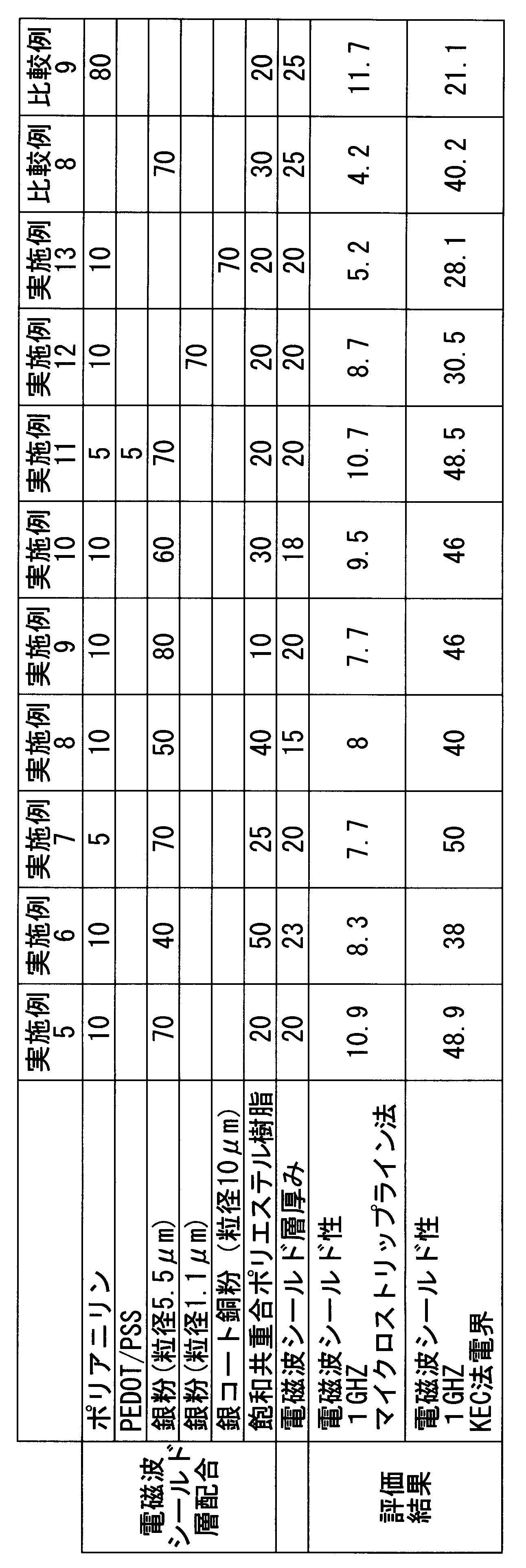
表2から明らかなように、実施例5~13では、1GHzのように高周波帯域の電磁波であっても、電磁波を吸収することで効果的に遮断されている結果が得られた。
これに対して、比較例では、実施例5~13と比較すると、高周波帯域の電磁波が効果的に遮断されているとはいえない結果であった。
以下の実施例14~34及び比較例10~13において使用した原材料は以下のとおりである。
PPET1501SG30 東亞合成社製 スチレン系エラストマー
MHM-GAW25 日栄化工社製 アクリル系樹脂
NeoFix20 日栄化工社製 表面アクリル樹脂PETフィルム
NeoFix10 日栄化工社製 表面アクリル樹脂PETフィルム
NeoFix5S2 日栄化工社製 表面アクリル樹脂PETフィルム
630RF 富士化学社製 スチレンブタジエンゴム系樹脂
T4100 東洋紡社製 延伸PET
GL-10 日栄化工社製 表面アクリル樹脂PETフィルム
GL-5B 日栄化工社製 表面アクリル樹脂PETフィルム
FIK フタムラ化学社製 無延伸ポリプロピレン
FOA フタムラ化学社製 延伸ポリプロピレン
PPET1501SG30 東亞合成社製 スチレン系エラストマー
MHM-GAW25 日栄化工社製 アクリル系樹脂
NeoFix20 日栄化工社製 表面アクリル樹脂PETフィルム
NeoFix10 日栄化工社製 表面アクリル樹脂PETフィルム
NeoFix5S2 日栄化工社製 表面アクリル樹脂PETフィルム
630RF 富士化学社製 スチレンブタジエンゴム系樹脂
T4100 東洋紡社製 延伸PET
GL-10 日栄化工社製 表面アクリル樹脂PETフィルム
GL-5B 日栄化工社製 表面アクリル樹脂PETフィルム
FIK フタムラ化学社製 無延伸ポリプロピレン
FOA フタムラ化学社製 延伸ポリプロピレン
<ワニスの調製>
飽和共重合ポリエステル樹脂(東洋紡(株)社製)20質量部、ポリアニリン((株)レグルス社製 PANT)10質量部、鱗片状銀粉(福田金属箔粉工業社製、Ag-XF301 平均粒子径5.5μm)70質量部をトルエン20部に分散させ、超音波をあてることで均一化し、ワニスを調製した。
飽和共重合ポリエステル樹脂(東洋紡(株)社製)20質量部、ポリアニリン((株)レグルス社製 PANT)10質量部、鱗片状銀粉(福田金属箔粉工業社製、Ag-XF301 平均粒子径5.5μm)70質量部をトルエン20部に分散させ、超音波をあてることで均一化し、ワニスを調製した。
(実施例14)
<電磁波シールド用フィルムの製造>
電磁波シールド用フィルムを得るために、絶縁層を構成する樹脂として、スチレン系エラストマー(東亞合成社製、品番PPET1501SG30)を準備した。電磁波遮断層を構成する樹脂として、前記で調製したワニスを準備した。
<電磁波シールド用フィルムの製造>
電磁波シールド用フィルムを得るために、絶縁層を構成する樹脂として、スチレン系エラストマー(東亞合成社製、品番PPET1501SG30)を準備した。電磁波遮断層を構成する樹脂として、前記で調製したワニスを準備した。
前記ワニスをポリエチレンテレフタレートフィルム(帝人デュポン製、A-314、厚み38μm)にコンマコーター塗工し、前記絶縁層とラミネートした。ポリエチレンテレフタレートフィルム(帝人デュポン製、A-314、厚み38μm)を剥離して電磁波シールド用フィルムを作製した。
実施例14の電磁波シールド用フィルムの全体の厚みは、49μmであり、電磁波遮断層の厚みは24μm、絶縁層の厚みは25μmであった。
(実施例15~19、24~27、34、比較例10,11,13)
表3~5の原材料を用いて、実施例14と同様にして電磁波シールド用フィルムを作製した。
表3~5の原材料を用いて、実施例14と同様にして電磁波シールド用フィルムを作製した。
(実施例20)
<電磁波シールド用フィルムの製造>
電磁波シールド用フィルムを得るために、保護層を構成する樹脂としてスチレンブタジエンゴム系樹脂(富士化学社製630RF)を準備した。絶縁層を構成する樹脂として、スチレン系エラストマー(東亜化学製、品番PPET1501SG30)を準備した。電磁波遮断層を構成する樹脂として、前記で調製したワニスを準備した。
<電磁波シールド用フィルムの製造>
電磁波シールド用フィルムを得るために、保護層を構成する樹脂としてスチレンブタジエンゴム系樹脂(富士化学社製630RF)を準備した。絶縁層を構成する樹脂として、スチレン系エラストマー(東亜化学製、品番PPET1501SG30)を準備した。電磁波遮断層を構成する樹脂として、前記で調製したワニスを準備した。
前記ワニスをポリエチレンテレフタレートフィルム(帝人デュポン製、A-314、厚み38μm)にコンマコーター塗工し、前記絶縁層とラミネートした。ポリエチレンテレフタレートフィルム(帝人デュポン製、A-314、厚み38μm)を剥離し、剥離面側に前記保護層をラミネートして電磁波シールド用フィルムを作製した。
実施例20の電磁波シールド用フィルムの全体の厚みは、26μmであり、保護層の厚みは15μm、電磁波遮断層の厚みは6μm、絶縁層の厚みは5μmであった。
(実施例21~23、28~33、比較例12)
表3~5の原材料を用いて、実施例20と同様にして電磁波シールド用フィルムを作製した。
表3~5の原材料を用いて、実施例20と同様にして電磁波シールド用フィルムを作製した。
<成形追従性>
実施例および比較例で作製した電磁波シールド用フィルムについて、コンデンサーが一定間隔で搭載された基板上にプレス機にて25℃、0.1MPaで20秒貼り付けし、コンデンサー段差におけるフィルム成形追従性を目視で測定した。
判定基準は以下の通りである。
○:コンデンサー周辺でフィルムが十分追従している
×:コンデンサー周辺でフィルムが追従しておらずフィルムの浮きが多い
実施例および比較例で作製した電磁波シールド用フィルムについて、コンデンサーが一定間隔で搭載された基板上にプレス機にて25℃、0.1MPaで20秒貼り付けし、コンデンサー段差におけるフィルム成形追従性を目視で測定した。
判定基準は以下の通りである。
○:コンデンサー周辺でフィルムが十分追従している
×:コンデンサー周辺でフィルムが追従しておらずフィルムの浮きが多い
<接着強度>
電磁波シールド用フィルムをポリイミドフィルム(カネカ社製、品番アピカル)に、25℃、0.1MPaで20秒貼り合わせたサンプルを、JIS Z0237に準拠し、25mm幅、引きはがし角度180°で引きはがして、ポリイミドフィルムとの密着性を測定した。
電磁波シールド用フィルムをポリイミドフィルム(カネカ社製、品番アピカル)に、25℃、0.1MPaで20秒貼り合わせたサンプルを、JIS Z0237に準拠し、25mm幅、引きはがし角度180°で引きはがして、ポリイミドフィルムとの密着性を測定した。
<電磁波シールド性>
実施例および比較例で作製した電磁波シールド用フィルムについて、マイクロストリップライン法を用いて、周波数1GHzにおける電磁波を遮断する電磁波シールド性を測定した。さらに、KEC法を用いて、周波数1GHzにおける電磁波を遮断する電磁波シールド性を測定した。
実施例および比較例で作製した電磁波シールド用フィルムについて、マイクロストリップライン法を用いて、周波数1GHzにおける電磁波を遮断する電磁波シールド性を測定した。さらに、KEC法を用いて、周波数1GHzにおける電磁波を遮断する電磁波シールド性を測定した。
結果を表3~5に示す。
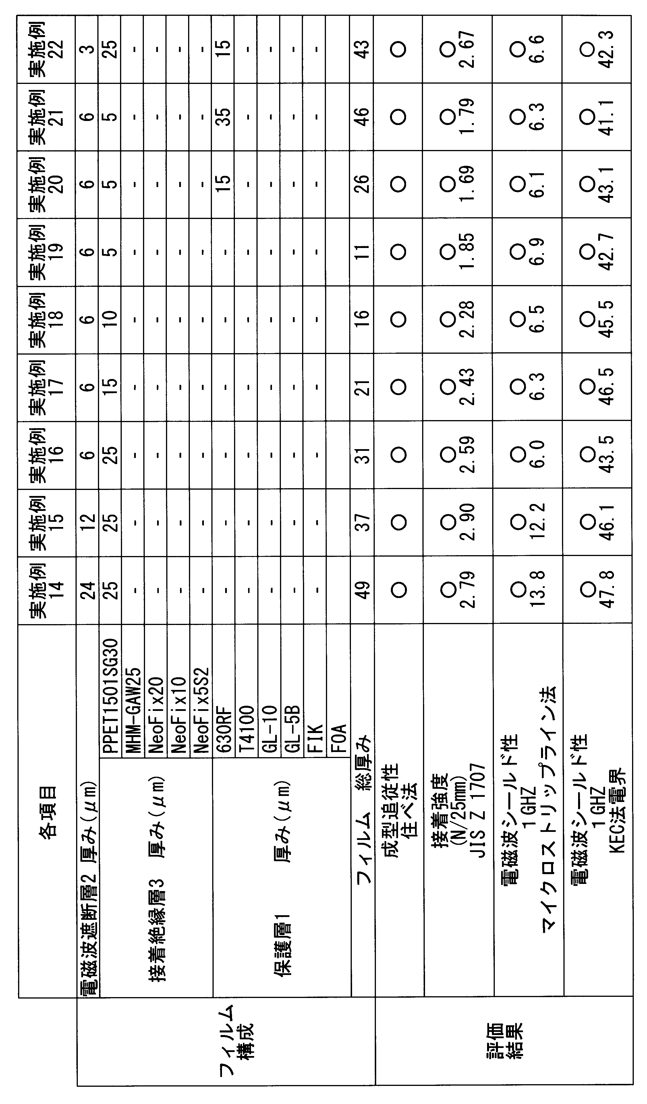

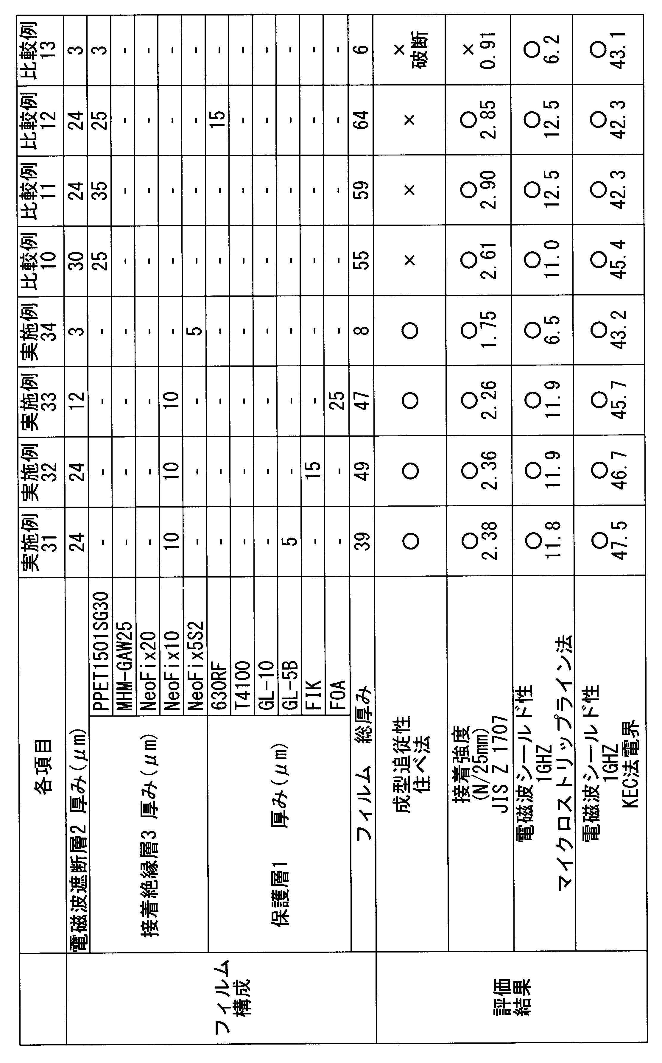
フィルム厚みが8μm以上50μm以下の電磁波シールド用フィルムを用いた実施例14~34では、成形追従性が良好であった。しかし、上記範囲を満たさないフィルムを用いた比較例では、成形追従性が満足できるものではなかった。
(実施例35)
<ワニスの調製>
飽和共重合ポリエステル樹脂(東洋紡(株)社製)20質量部、ポリアニリン((株)レグルス社製 PANT)10質量部、鱗片状銀粉(福田金属箔粉工業社製、Ag-XF301 平均粒子径5.5μm)70質量部をトルエン20部に分散させ、超音波をあてることで均一化し、ワニスを調製した。
<ワニスの調製>
飽和共重合ポリエステル樹脂(東洋紡(株)社製)20質量部、ポリアニリン((株)レグルス社製 PANT)10質量部、鱗片状銀粉(福田金属箔粉工業社製、Ag-XF301 平均粒子径5.5μm)70質量部をトルエン20部に分散させ、超音波をあてることで均一化し、ワニスを調製した。
<電磁波シールド用フィルムの製造>
電磁波シールド用フィルムを得るために、保護層を構成する樹脂としてポリエチレンテレフタラート(東洋紡(株)社製品番T-4100)を準備した。絶縁層を構成する樹脂として、PET両面テープ(日栄化工社製、品番NeoFix20 表面アクリル樹脂)を準備した。電磁波遮断層を構成する樹脂として、前記で調整したワニスを準備した。
電磁波シールド用フィルムを得るために、保護層を構成する樹脂としてポリエチレンテレフタラート(東洋紡(株)社製品番T-4100)を準備した。絶縁層を構成する樹脂として、PET両面テープ(日栄化工社製、品番NeoFix20 表面アクリル樹脂)を準備した。電磁波遮断層を構成する樹脂として、前記で調整したワニスを準備した。
前記ワニスをポリエチレンテレフタレートフィルム(帝人デュポン製、A-314、厚み38μm)にコンマコーター塗工し、前記絶縁層とラミネートした。ポリエチレンテレフタレートフィルム(帝人デュポン製、A-314、厚み38μm)を剥離し、剥離面側に前記基材層をラミネートして電磁波シールド用フィルムを作製した。
実施例35の電磁波シールド用フィルムの全体の厚みは、49μmであり、基材層の厚みは9μm、電磁波遮断層の厚みは20μm、絶縁層の厚みは20μmであった。
(実施例36)
絶縁層を構成する樹脂としてPET両面テープ(日栄化工(株)社製、品番NeoFix10 表面アクリル樹脂)を用いた以外は実施例35と同様にして、電磁波シールド用フィルムを作製した。
絶縁層を構成する樹脂としてPET両面テープ(日栄化工(株)社製、品番NeoFix10 表面アクリル樹脂)を用いた以外は実施例35と同様にして、電磁波シールド用フィルムを作製した。
(実施例37)
絶縁層を構成する樹脂としてPET両面テープ(日栄化工(株)社製、品番NeoFix5S2 表面アクリル樹脂)を用いた以外は実施例35と同様にして、電磁波シールド用フィルムを作製した。
絶縁層を構成する樹脂としてPET両面テープ(日栄化工(株)社製、品番NeoFix5S2 表面アクリル樹脂)を用いた以外は実施例35と同様にして、電磁波シールド用フィルムを作製した。
(実施例38)
絶縁層を構成する樹脂としてスチレン系エラストマー(東亞合成(株)社製、品番PPET-1501SG30)を25μm厚で塗工して用いた以外は実施例35と同様にして、電磁波シールド用フィルムを作製した。
絶縁層を構成する樹脂としてスチレン系エラストマー(東亞合成(株)社製、品番PPET-1501SG30)を25μm厚で塗工して用いた以外は実施例35と同様にして、電磁波シールド用フィルムを作製した。
(比較例14)
絶縁層を構成する樹脂としてアクリル樹脂(日栄化工(株)社製、品番MHM-GAW)を用いた以外は実施例35と同様にして、電磁波シールド用フィルムを作製した。
絶縁層を構成する樹脂としてアクリル樹脂(日栄化工(株)社製、品番MHM-GAW)を用いた以外は実施例35と同様にして、電磁波シールド用フィルムを作製した。
<評価試験>
実施例35~38、および比較例14で作製した電磁波シールド用フィルム、または電子部品について、ポリイミドとの密着性、破断性、突き刺し強度の評価を行った。以下に、これらの評価方法について説明する。
実施例35~38、および比較例14で作製した電磁波シールド用フィルム、または電子部品について、ポリイミドとの密着性、破断性、突き刺し強度の評価を行った。以下に、これらの評価方法について説明する。
<<ポリイミドフィルムとの密着性>>
電磁波シールド用フィルムをポリイミドフィルム(カネカ社製、品番アピカル)に、25℃、0.1MPaで20秒貼り合わせたサンプルを、JIS Z0237に準拠し、25mm幅、引きはがし角度180°で引きはがして、ポリイミドフィルムとの密着性を測定した。
電磁波シールド用フィルムをポリイミドフィルム(カネカ社製、品番アピカル)に、25℃、0.1MPaで20秒貼り合わせたサンプルを、JIS Z0237に準拠し、25mm幅、引きはがし角度180°で引きはがして、ポリイミドフィルムとの密着性を測定した。
<<破断性>>
テスターを用いて、前記プリント配線板の金属部分と電磁波遮蔽層との間での電流の有無を確認することで、破断の有無を判断した。すなわち、電流が流れたものを破断有りとし、電流が流れなかったものを、破断無しと判断した。
テスターを用いて、前記プリント配線板の金属部分と電磁波遮蔽層との間での電流の有無を確認することで、破断の有無を判断した。すなわち、電流が流れたものを破断有りとし、電流が流れなかったものを、破断無しと判断した。
<<突き刺し強度>>
(突き刺し強度測定用フィルムの作製)
絶縁層を構成する樹脂フィルムをそのまま用いて、突き刺し強度測定用フィルムとした。
(突き刺し強度測定用フィルムの作製)
絶縁層を構成する樹脂フィルムをそのまま用いて、突き刺し強度測定用フィルムとした。
前記、絶縁層に用いたフィルム単体について、JIS Z 1707に準拠して、先端部直径1mmの針を、突き刺し速度50mm/分でフィルムに突き刺し、針がフィルムを貫通する際の強度を測定し、突き刺し強度とした。
結果を表6に示す。

絶縁層の、JISZ1707で測定した突き刺し強度が0.90N以上10.0N以下である電磁波シールド用フィルムを用いた実施例1~4では、破断性が良好であった。しかし、上記範囲を満たさないフィルムを用いた比較例では、破断性が満足できるものではなかった。
本発明の電磁波シールドフィルムは、電子部品の軽量化・薄型化に対応できるため、産業上極めて有用である。
100 電磁波シールドフィルム
1 基材層
11 第1の層
12 第3の層
13 第2の層
2 絶縁層
3 電磁波遮断層
31 吸収層
32 反射層
4 電子部品
5 基板
6 凹凸
61 凸部
62 凹部
201 保護層
202 電磁波遮断層
203 絶縁層
1 基材層
11 第1の層
12 第3の層
13 第2の層
2 絶縁層
3 電磁波遮断層
31 吸収層
32 反射層
4 電子部品
5 基板
6 凹凸
61 凸部
62 凹部
201 保護層
202 電磁波遮断層
203 絶縁層
Claims (39)
- 電磁波シールドフィルムであって、
少なくとも基材層と、電磁波遮断層とを順に積層し、
前記電磁波遮断層は、Z折りを行ったときにその両端間で導電性を有する組成物から形成されることを特徴とする電磁波シールドフィルム。 - 前記電磁波遮断層は、導電性組成物及びバインダーを含有し、
前記バインダーが非晶質熱可塑性樹脂を主成分とすることを特徴とする請求項1に記載の電磁波シールドフィルム。 - 前記バインダーが15質量%以上55質量%以下の配合量であることを特徴とする請求項1または2に記載の電磁波シールドフィルム。
- 前記非晶質熱可塑性樹脂が非晶質ポリエステル系樹脂であることを特徴とする請求項1ないし3のいずれか1項に記載の電磁波シールドフィルム。
- 前記基材層は、少なくとも2つの層が積層された積層体を備えることを特徴とする請求項1ないし4のいずれか1項に記載の電磁波シールドフィルム。
- 前記基材層は、第1の層と、第2の層と、第3の層とが順に積層された積層体であることを特徴とする請求項1ないし5のいずれか1項に記載の電磁波シールドフィルム。
- 前記第1の層の厚さT(A)と前記第2の層の厚さT(C)と前記第3の層の厚さT(B)が下記式(1)を満たすことを特徴とする請求項1ないし6のいずれか1項に記載の電磁波シールドフィルム。
0.05<T(C)/(T(A)+T(B))<10・・・(1) - さらに、絶縁層を前記基材層の表面あるいは前記電磁波遮断層の表面に積層することを特徴とする請求項1ないし7のいずれか1項に記載の電磁波シールドフィルム。
- 電子部品を搭載する基板であって、
請求項1ないし8のいずれか1項に記載の電磁波シールドフィルムを基板上の凹凸の被覆部材として備え、
前記凹凸は、1mm以上の段差を有することを特徴とする基板。 - 請求項1ないし8のいずれか1項に記載の電磁波シールドフィルムを電磁波遮蔽部材として備えることを特徴とするフレキシブルプリント基板。
- 基材層と、該基材層に積層された、電磁波遮断層とを含んで構成され、
前記電磁波遮断層は、導電性高分子と、金属粉を含有することを特徴する電磁波シールド用フィルム。 - 前記導電性高分子は、ポリエチレンジオキシチオフェン/ポリスチレンスルホネート(PEDOT/PSS)およびポリアニリンのうちの少なくとも1種である請求項11に記載の電磁波シールド用フィルム。
- 前記金属粉は、銀粉もしくは銀コート銅粉である、請求項11または12に記載の電磁波シールド用フィルム。
- 前記電磁波遮断層は、周波数0.2~10GHzの電磁波における、マイクロストリップライン法を用いて測定した際の電磁波シールド効果が5dB以上である請求項11ないし13のいずれか1項に記載の電磁波シールド用フィルム。
- 前記電磁波遮断層は、周波数0.2~1GHzの電磁波における、KEC法を用いて測定した際の電磁波シールド効果が25dB以上である請求項11ないし14のいずれか1項に記載の電磁波シールド用フィルム。
- 前記電磁波遮断層の厚さは、1μm以上、100μm以下である請求項11ないし15のいずれか1項に記載の電磁波シールド用フィルム。
- 前記電磁波遮断層の前記基材層側の面、または前記基材層と反対側の面に積層された絶縁層を備える請求項11ないし16のいずれか1項に記載の電磁波シールド用フィルム。
- 当該電磁波シールド用フィルムは、基板上の凹凸を被覆するために用いられる請求項11ないし17のいずれか1項に記載の電磁波シールド用フィルム。
- 基板と、該基板上に搭載された電子部品と、前記基板の前記電子部品が搭載されている面側から前記基板および電子部品を被覆する、導電性高分子を主材料として含有する電磁波遮断層とを有する電子部品搭載基板であって、
前記電磁波遮断層は、導電性高分子と、金属粉を含有することを特徴する電子部品搭載基板。 - 基板上の凹凸を被覆するために用いられる電磁波シールド用フィルムであって、
絶縁層と該絶縁層の一方の面側に積層された電磁波遮断層を含んで構成され、
厚みが8μm以上50μm以下であることを特徴とする電磁波シールド用フィルム。 - 前記絶縁層とは反対側に電磁波遮断層を介して保護層が積層されている請求項20記載の電磁波シールド用フィルム。
- 前記絶縁層の厚みは、5μm以上25μm以下であることを特徴とする請求項20または21に記載の電磁波シールド用フィルム。
- 前記絶縁層は、熱可塑性を有する絶縁樹脂で構成されていることを特徴とする請求項20ないし22のいずれか1項に記載の電磁波シールド用フィルム。
- 前記絶縁層は、アクリル樹脂もしくはスチレン系エラストマーを含むことを特徴とする請求項20ないし23のいずれか1項に記載の電磁波シールド用フィルム。
- 前記電磁波遮断層は導電性高分子を含有することを特徴とする請求項20ないし24のいずれか1項に記載の電磁波シールド用フィルム。
- 前記導電性高分子が、ポリエチレンジオキシチオフェン/ポリスチレンスルホネート(PEDOT/PSS)およびポリアニリンのうちの少なくとも1種であることを特徴とする請求項25に記載の電磁波シールド用フィルム。
- 前記電磁波遮断層が、金属粉を含有することを特徴とする請求項20ないし26のいずれか1項に記載の電磁波シールド用フィルム。
- 前記金属粉は、銀粉もしくは銀コート銅粉であることを特徴とする請求項20ないし27のいずれか1項に記載の電磁波シールド用フィルム。
- 前記電磁波遮断層の厚さは3μm以上、25μm以下であることを特徴とする請求項20ないし27のいずれか1項に記載の電磁波シールド用フィルム。
- 基板上の凹凸を被覆するために用いられる電磁波シールド用フィルムであって、
絶縁層と該絶縁層の一方の面側に積層された電磁波遮断層を含んで構成され、
前記絶縁層のJIS Z 1707で測定した突き刺し強度が、0.90N以上10.0N以下であることを特徴とする電磁波シールド用フィルム。 - 前記絶縁層とは反対側に電磁波遮断層を介して保護層が積層されている請求項30記載の電磁波シールド用フィルム。
- 前記絶縁層は、熱可塑性を有する絶縁樹脂で構成されていることを特徴とする請求項30または31に記載の電磁波シールド用フィルム。
- 前記絶縁層の厚みは、3μm以上、50μm以下であることを特徴とする請求項30ないし32のいずれか1項に記載の電磁波シールド用フィルム。
- 前記電磁波遮断層は導電性高分子を含有することを特徴とする請求項30ないし33のいずれか1項に記載の電磁波シールド用フィルム。
- 前記導電性高分子が、ポリエチレンジオキシチオフェン/ポリスチレンスルホネート(PEDOT/PSS)およびポリアニリンのうちの少なくとも1種であることを特徴とする請求項34に記載の電磁波シールド用フィルム。
- 前記電磁波遮断層が、金属粉を含有することを特徴とする請求項30ないし35のいずれか1項に記載の電磁波シールド用フィルム。
- 前記金属粉は、銀粉もしくは銀コート銅粉であることを特徴とする請求項36に記載の電磁波シールド用フィルム。
- 前記電磁波遮断層の厚さは1μm以上、100μm以下であることを特徴とする請求項30ないし37のいずれか1項に記載の電磁波シールド用フィルム。
- ポリイミドフィルムとの密着力が、1N/25mm以上、100N/25mm以下であることを特徴とする請求項30ないし38のいずれか1項に記載の電磁波シールド用フィルム。
Applications Claiming Priority (8)
| Application Number | Priority Date | Filing Date | Title |
|---|---|---|---|
| JP2014-033732 | 2014-02-25 | ||
| JP2014033732A JP2015159214A (ja) | 2014-02-25 | 2014-02-25 | 電磁波シールドフィルム及びフレキシブルプリント基板 |
| JP2014108082 | 2014-05-26 | ||
| JP2014-108082 | 2014-05-26 | ||
| JP2014-184019 | 2014-09-10 | ||
| JP2014184019A JP2016058565A (ja) | 2014-09-10 | 2014-09-10 | 電磁波シールド用フィルム |
| JP2014187193A JP6497009B2 (ja) | 2014-09-16 | 2014-09-16 | 電磁波シールド用フィルム |
| JP2014-187193 | 2014-09-16 |
Publications (1)
| Publication Number | Publication Date |
|---|---|
| WO2015129546A1 true WO2015129546A1 (ja) | 2015-09-03 |
Family
ID=54008867
Family Applications (1)
| Application Number | Title | Priority Date | Filing Date |
|---|---|---|---|
| PCT/JP2015/054654 Ceased WO2015129546A1 (ja) | 2014-02-25 | 2015-02-19 | 電磁波シールドフィルム、フレキシブルプリント基板、電子部品搭載基板、及び電子部品の被覆方法 |
Country Status (2)
| Country | Link |
|---|---|
| TW (1) | TW201540171A (ja) |
| WO (1) | WO2015129546A1 (ja) |
Cited By (7)
| Publication number | Priority date | Publication date | Assignee | Title |
|---|---|---|---|---|
| CN105398662A (zh) * | 2015-11-12 | 2016-03-16 | 太仓市其盛化纤厂 | 防静电屏蔽袋 |
| JP2017063158A (ja) * | 2015-09-25 | 2017-03-30 | 住友ベークライト株式会社 | 電磁波シールド用フィルム、および電子部品搭載基板 |
| WO2019152762A1 (en) | 2018-02-01 | 2019-08-08 | Henkel IP & Holding GmbH | Method for shielding system-in-package assemblies from electromagnetic interference |
| CN110769677A (zh) * | 2018-07-27 | 2020-02-07 | 广州方邦电子股份有限公司 | 电磁屏蔽膜、线路板及电磁屏蔽膜的制备方法 |
| CN114292601A (zh) * | 2021-12-10 | 2022-04-08 | 苏州益邦电子材料有限公司 | 一种吸波绝缘支撑式保护片及保护片卷料 |
| CN116547140A (zh) * | 2020-12-09 | 2023-08-04 | Jx金属株式会社 | 电磁波屏蔽材料 |
| DE102023111773A1 (de) * | 2023-05-05 | 2024-11-07 | Elringklinger Ag | Schutzelement, Energieversorgungssystem, Kommunikationssystem und Kraftfahrzeug |
Families Citing this family (3)
| Publication number | Priority date | Publication date | Assignee | Title |
|---|---|---|---|---|
| JP6407395B1 (ja) * | 2017-12-01 | 2018-10-17 | タツタ電線株式会社 | 電磁波シールドフィルム |
| JP6497477B1 (ja) * | 2018-10-03 | 2019-04-10 | 東洋インキScホールディングス株式会社 | 電磁波シールドシート、および電子部品搭載基板 |
| TWI832393B (zh) * | 2022-08-24 | 2024-02-11 | 易鼎股份有限公司 | 電路板之導電凸塊結構及其製造方法 |
Citations (5)
| Publication number | Priority date | Publication date | Assignee | Title |
|---|---|---|---|---|
| WO2008108099A1 (ja) * | 2007-03-05 | 2008-09-12 | Kyodo Giken Chemical Co., Ltd. | 導電性高分子弾性体組成物及び該組成物から成る電磁波シールド |
| JP2009543931A (ja) * | 2006-07-17 | 2009-12-10 | イー・アイ・デュポン・ドウ・ヌムール・アンド・カンパニー | 金属組成物、熱画像形成ドナーおよびそれらから得られたパターン化多層組成物 |
| JP2012186222A (ja) * | 2011-03-03 | 2012-09-27 | Nagase Chemtex Corp | 成型用電磁波シールドシート及び電磁波シールド成型体 |
| WO2014027672A1 (ja) * | 2012-08-16 | 2014-02-20 | 住友ベークライト株式会社 | 電磁波シールド用フィルム、および電子部品の被覆方法 |
| WO2015052742A1 (ja) * | 2013-10-07 | 2015-04-16 | 出光興産株式会社 | ノイズ吸収積層体 |
-
2015
- 2015-02-19 WO PCT/JP2015/054654 patent/WO2015129546A1/ja not_active Ceased
- 2015-02-25 TW TW104105977A patent/TW201540171A/zh unknown
Patent Citations (5)
| Publication number | Priority date | Publication date | Assignee | Title |
|---|---|---|---|---|
| JP2009543931A (ja) * | 2006-07-17 | 2009-12-10 | イー・アイ・デュポン・ドウ・ヌムール・アンド・カンパニー | 金属組成物、熱画像形成ドナーおよびそれらから得られたパターン化多層組成物 |
| WO2008108099A1 (ja) * | 2007-03-05 | 2008-09-12 | Kyodo Giken Chemical Co., Ltd. | 導電性高分子弾性体組成物及び該組成物から成る電磁波シールド |
| JP2012186222A (ja) * | 2011-03-03 | 2012-09-27 | Nagase Chemtex Corp | 成型用電磁波シールドシート及び電磁波シールド成型体 |
| WO2014027672A1 (ja) * | 2012-08-16 | 2014-02-20 | 住友ベークライト株式会社 | 電磁波シールド用フィルム、および電子部品の被覆方法 |
| WO2015052742A1 (ja) * | 2013-10-07 | 2015-04-16 | 出光興産株式会社 | ノイズ吸収積層体 |
Cited By (9)
| Publication number | Priority date | Publication date | Assignee | Title |
|---|---|---|---|---|
| JP2017063158A (ja) * | 2015-09-25 | 2017-03-30 | 住友ベークライト株式会社 | 電磁波シールド用フィルム、および電子部品搭載基板 |
| CN105398662A (zh) * | 2015-11-12 | 2016-03-16 | 太仓市其盛化纤厂 | 防静电屏蔽袋 |
| WO2019152762A1 (en) | 2018-02-01 | 2019-08-08 | Henkel IP & Holding GmbH | Method for shielding system-in-package assemblies from electromagnetic interference |
| EP3747049A4 (en) * | 2018-02-01 | 2021-10-27 | Henkel IP & Holding GmbH | PROCESS FOR SHIELDING SYSTEM-IN-PACKAGE ARRANGEMENTS AGAINST ELECTROMAGNETIC INTERFERENCE |
| CN110769677A (zh) * | 2018-07-27 | 2020-02-07 | 广州方邦电子股份有限公司 | 电磁屏蔽膜、线路板及电磁屏蔽膜的制备方法 |
| CN116547140A (zh) * | 2020-12-09 | 2023-08-04 | Jx金属株式会社 | 电磁波屏蔽材料 |
| CN116547140B (zh) * | 2020-12-09 | 2025-11-11 | Jx金属株式会社 | 电磁波屏蔽材料 |
| CN114292601A (zh) * | 2021-12-10 | 2022-04-08 | 苏州益邦电子材料有限公司 | 一种吸波绝缘支撑式保护片及保护片卷料 |
| DE102023111773A1 (de) * | 2023-05-05 | 2024-11-07 | Elringklinger Ag | Schutzelement, Energieversorgungssystem, Kommunikationssystem und Kraftfahrzeug |
Also Published As
| Publication number | Publication date |
|---|---|
| TW201540171A (zh) | 2015-10-16 |
Similar Documents
| Publication | Publication Date | Title |
|---|---|---|
| JP6263846B2 (ja) | 電磁波シールド用フィルム、および電子部品の被覆方法 | |
| JP6481612B2 (ja) | 電磁波シールド用フィルム、および電子部品搭載基板 | |
| TW201540171A (zh) | 電磁波遮蔽膜、撓性印刷基板、電子零件搭載基板、及電子零件之被覆方法 | |
| KR102400969B1 (ko) | 전자 부품 탑재 기판 및 전자 기기 | |
| KR102311989B1 (ko) | 전자파 차폐 시트 | |
| CN110324959A (zh) | 电磁波屏蔽膜、屏蔽印制线路板及屏蔽印制线路板的制造方法 | |
| JP2019009452A (ja) | 電子部品搭載基板、積層体、電磁波遮蔽シートおよび電子機器 | |
| JP2019009396A (ja) | 電磁波シールド用フィルム、および電子部品搭載基板 | |
| JP2015159214A (ja) | 電磁波シールドフィルム及びフレキシブルプリント基板 | |
| JP2020098905A (ja) | 電子部品搭載基板および電子機器 | |
| JP6497009B2 (ja) | 電磁波シールド用フィルム | |
| JP2016006808A (ja) | 電磁波シールド用フィルム、および電子部品搭載基板 | |
| JP2018129493A (ja) | 部品搭載基板の製造方法 | |
| JP6451801B1 (ja) | 電磁波シールド電子機器の製造方法、および前記電磁波シールド電子機器の製造方法に用いられる電磁波シールドフィルム | |
| JP2020098896A (ja) | 電子部品搭載基板および電子機器 | |
| JP2016058565A (ja) | 電磁波シールド用フィルム | |
| JP7099365B2 (ja) | 電磁波シールドシート、部品搭載基板、および電子機器 | |
| JP2016009809A (ja) | 電磁波シールド用フィルム、および電子部品搭載基板 | |
| JP2019106492A (ja) | 封止用フィルムおよび封止用フィルム被覆電子部品搭載基板 | |
| JP2017063158A (ja) | 電磁波シールド用フィルム、および電子部品搭載基板 | |
| CN120547857A (zh) | 一种电磁屏蔽膜及线路板 |
Legal Events
| Date | Code | Title | Description |
|---|---|---|---|
| 121 | Ep: the epo has been informed by wipo that ep was designated in this application |
Ref document number: 15755502 Country of ref document: EP Kind code of ref document: A1 |
|
| NENP | Non-entry into the national phase |
Ref country code: DE |
|
| 122 | Ep: pct application non-entry in european phase |
Ref document number: 15755502 Country of ref document: EP Kind code of ref document: A1 |