WO2015129392A1 - 基板処理方法、コンピュータ記憶媒体及び基板処理システム - Google Patents
基板処理方法、コンピュータ記憶媒体及び基板処理システム Download PDFInfo
- Publication number
- WO2015129392A1 WO2015129392A1 PCT/JP2015/052826 JP2015052826W WO2015129392A1 WO 2015129392 A1 WO2015129392 A1 WO 2015129392A1 JP 2015052826 W JP2015052826 W JP 2015052826W WO 2015129392 A1 WO2015129392 A1 WO 2015129392A1
- Authority
- WO
- WIPO (PCT)
- Prior art keywords
- polymer
- solvent
- block copolymer
- substrate
- wafer
- Prior art date
- Legal status (The legal status is an assumption and is not a legal conclusion. Google has not performed a legal analysis and makes no representation as to the accuracy of the status listed.)
- Ceased
Links
Images







Classifications
-
- H—ELECTRICITY
- H10—SEMICONDUCTOR DEVICES; ELECTRIC SOLID-STATE DEVICES NOT OTHERWISE PROVIDED FOR
- H10P—GENERIC PROCESSES OR APPARATUS FOR THE MANUFACTURE OR TREATMENT OF DEVICES COVERED BY CLASS H10
- H10P95/00—Generic processes or apparatus for manufacture or treatments not covered by the other groups of this subclass
- H10P95/08—Planarisation of organic insulating materials
-
- H—ELECTRICITY
- H10—SEMICONDUCTOR DEVICES; ELECTRIC SOLID-STATE DEVICES NOT OTHERWISE PROVIDED FOR
- H10P—GENERIC PROCESSES OR APPARATUS FOR THE MANUFACTURE OR TREATMENT OF DEVICES COVERED BY CLASS H10
- H10P72/00—Handling or holding of wafers, substrates or devices during manufacture or treatment thereof
- H10P72/30—Handling or holding of wafers, substrates or devices during manufacture or treatment thereof for conveying, e.g. between different workstations
- H10P72/33—Handling or holding of wafers, substrates or devices during manufacture or treatment thereof for conveying, e.g. between different workstations into and out of processing chamber
- H10P72/3306—Horizontal transfer of a single workpiece
-
- H—ELECTRICITY
- H10—SEMICONDUCTOR DEVICES; ELECTRIC SOLID-STATE DEVICES NOT OTHERWISE PROVIDED FOR
- H10P—GENERIC PROCESSES OR APPARATUS FOR THE MANUFACTURE OR TREATMENT OF DEVICES COVERED BY CLASS H10
- H10P76/00—Manufacture or treatment of masks on semiconductor bodies, e.g. by lithography or photolithography
- H10P76/20—Manufacture or treatment of masks on semiconductor bodies, e.g. by lithography or photolithography of masks comprising organic materials
Definitions
- the present invention relates to a substrate processing method using a block copolymer comprising a hydrophilic (polar) polymer having hydrophilicity (polarity) and a hydrophobic (nonpolar) polymer having hydrophobicity (no polarity).
- the present invention relates to a computer storage medium and a substrate processing system.
- a resist coating process for coating a resist solution on a semiconductor wafer to form a resist film
- an exposure process for exposing a predetermined pattern on the resist film A photolithography process for sequentially performing a development process for developing the exposed resist film is performed to form a predetermined resist pattern on the wafer.
- an etching process is performed on the film to be processed on the wafer, and then a resist film removing process is performed to form a predetermined pattern on the film to be processed.
- Patent Document 1 a wafer processing method using a block copolymer composed of two types of block chains (polymer), hydrophilic and hydrophobic, has been proposed (Patent Document 1).
- a neutral layer having an intermediate affinity for two types of polymers is formed on a wafer, and a guide pattern is formed on the neutral layer by using, for example, a resist.
- a block copolymer is applied onto the neutral layer, and the block copolymer is subjected to a heat treatment or an annealing treatment in a solvent atmosphere to cause phase separation into a hydrophilic polymer and a hydrophobic polymer.
- the processing target film is etched using the polymer pattern as a mask to form a predetermined pattern on the processing target film.
- the block copolymer is phase-separated by an annealing treatment in a solvent atmosphere, the pattern due to the polymer after phase separation may vary.
- the present inventors diligently investigated this point.
- the knowledge that it was caused by the difference in the solvent used was obtained. That is, the solvent for making the block copolymer into a solution is selected in consideration of wettability with the wafer for the purpose of uniform application to the wafer, while being used for annealing in a solvent atmosphere.
- the solvent to be used is selected considering the promotion of phase separation of the block copolymer.
- the present inventors further examined that before performing the annealing treatment in the solvent atmosphere, the solvent for the coating treatment contained in the block copolymer was removed, and the solvent was used in the annealing treatment in the solvent atmosphere. It was found that the dispersion of the pattern due to the polymer can be suppressed by preventing mixing.
- the present invention has been made in view of such points, and an object of the present invention is to appropriately form a predetermined pattern on a substrate in substrate processing using a block copolymer containing a hydrophilic polymer and a hydrophobic polymer.
- the present invention provides a substrate processing method for processing a substrate using a block copolymer containing a first polymer and a second polymer, A block copolymer coating step of coating the block copolymer on a substrate on which a predetermined pattern is formed; A solvent removal step of removing the solvent from the block copolymer by heat-treating the substrate after application of the block copolymer at a temperature equal to or higher than the volatilization temperature of the solvent contained in the block copolymer; Polymer separation in which the substrate after the solvent removal is annealed in an atmosphere of another solvent different from the removed solvent to phase-separate the block copolymer into the first polymer and the second polymer And having a process The annealing process in the polymer separation step is performed at a temperature lower than the volatilization temperature of the other solvent.
- the substrate coated with the block copolymer is heated at a temperature equal to or higher than the volatilization temperature of the solvent contained in the block copolymer to remove the solvent from the block copolymer, and then removed.
- the block copolymer is annealed in another solvent atmosphere different from the solvent. By this annealing treatment, other solvent penetrates into the block copolymer on the substrate, but at this point, the solvent already contained in the block copolymer at the time of the coating treatment has been removed. It does not mix with other solvents.
- the block copolymer can be favorably phase-separated into the first polymer and the second polymer in the annealing treatment.
- a predetermined pattern can be appropriately formed on the substrate in the substrate processing using the block copolymer including the first polymer and the second polymer.
- Another aspect of the present invention is a readable computer storage medium storing a program that operates on a computer of a control unit that controls the substrate processing system so that the substrate processing method is executed by the substrate processing system.
- a substrate processing system for processing a substrate using a block copolymer including a first polymer and a second polymer, on the substrate on which a predetermined pattern is formed.
- the block copolymer coating apparatus for coating the block copolymer, and the substrate after the block copolymer coating is heat-treated at a temperature equal to or higher than the volatilization temperature of the solvent contained in the block copolymer.
- a solvent removal apparatus for removing the solvent, and the substrate after the removal of the solvent are annealed in an atmosphere of another solvent different from the removed solvent, so that the block copolymer is converted into the first polymer and the first polymer.
- a polymer separator for phase-separating into two polymers, and the polymer separator so that annealing in the polymer separator is performed at a temperature lower than the volatilization temperature of the other solvent.
- a control unit for controlling.
- a predetermined pattern can be appropriately formed on a substrate in substrate processing using a block copolymer containing a hydrophilic polymer and a hydrophobic polymer.
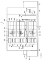
- FIG. 1 is an explanatory diagram showing an outline of a configuration of a substrate processing system 1 according to the present embodiment.
- 2 and 3 are a front view and a rear view showing an outline of the internal configuration of the substrate processing system 1.
- the substrate processing system 1 includes a cassette station 10 in which a cassette C containing a plurality of wafers W is loaded and unloaded, and a processing station 11 having a plurality of various processing apparatuses for performing predetermined processing on the wafers W. And an interface station 13 that transfers the wafer W to and from the exposure apparatus 12 adjacent to the processing station 11 is integrally connected.
- the cassette station 10 is provided with a cassette mounting table 20.
- the cassette mounting table 20 is provided with, for example, four cassette mounting plates 21 on which the cassette C is mounted when the cassette C is carried in and out of the substrate processing system 1.
- the cassette station 10 is provided with a wafer transfer device 23 that is movable on a transfer path 22 extending in the X direction as shown in FIG.
- the wafer transfer device 23 is also movable in the vertical direction and the vertical axis direction ( ⁇ direction), and includes a cassette C on each cassette mounting plate 21 and a delivery device for a third block G3 of the processing station 11 described later.
- the wafer W can be transferred between the two.
- the processing station 11 is provided with a plurality of, for example, four blocks G1, G2, G3, and G4 having various devices.
- the first block G1 is provided on the front side of the processing station 11 (X direction negative direction side in FIG. 1), and the second block is provided on the back side of the processing station 11 (X direction positive direction side in FIG. 1).
- Block G2 is provided.
- a third block G3 is provided on the cassette station 10 side (Y direction negative direction side in FIG. 1) of the processing station 11, and the interface station 13 side (Y direction positive direction side in FIG. 1) of the processing station 11 is provided. Is provided with a fourth block G4.
- a plurality of liquid processing apparatuses for example, a developing apparatus 30 for developing the wafer W, and a cleaning apparatus 31 for cleaning the wafer W by applying an organic solvent onto the wafer W are provided.
- An apparatus 34 and a block copolymer coating apparatus 35 for coating the block copolymer on the wafer W are stacked in order from the bottom.
- the developing device 30, the cleaning device 31, the antireflection film forming device 32, the processing liquid supply device 33, the resist coating device 34, and the block copolymer coating device 35 are arranged side by side in the horizontal direction.
- the number and arrangement of the developing device 30, the cleaning device 31, the antireflection film forming device 32, the processing liquid supply device 33, the resist coating device 34, and the block copolymer coating device 35 can be arbitrarily selected.
- the cleaning device 31, the antireflection film forming device 32, the processing liquid supply device 33, the resist coating device 34, and the block copolymer coating device 35 for example, spin coating that coats a predetermined coating solution on the wafer W. Is done.
- spin coating for example, a coating liquid is discharged onto the wafer W from a coating nozzle, and the wafer W is rotated to diffuse the coating liquid to the surface of the wafer W. The configuration of these liquid processing apparatuses will be described later.
- the block copolymer applied onto the wafer W by the block copolymer coating device 35 includes a first polymer and a second polymer.
- a hydrophilic polymer that is a polar (hydrophilic) polymer is used as the first polymer
- a hydrophobic polymer that is a non-polar (hydrophobic) polymer is used as the second polymer.
- PDMS polydimethylsiloxane
- PS polystyrene
- the molecular weight ratio of the hydrophilic polymer in the block copolymer is 20% to 40%, and the molecular weight ratio of the hydrophobic polymer in the block copolymer is 80% to 60%.
- the block copolymer is a polymer in which a hydrophilic polymer and a hydrophobic polymer are linearly combined, and a compound of these hydrophilic polymer and hydrophobic polymer is made into a solution with a solvent.
- heptane etc. are used for this solvent, for example.
- the processing liquid used in the processing liquid supply device 33 is, for example, a polystyrene solution.
- a polystyrene solution For example, by supplying polystyrene to the wafer W after the resist pattern is formed, a polystyrene film is formed on the surface of the resist pattern.
- the block copolymer coated on the wafer W by the heat treatment apparatus 40 for performing the heat treatment of the wafer W and the block copolymer coating apparatus 35 is annealed in a solvent atmosphere.
- a post-phase separation heat treatment device 44 for removing the solvent by heat treatment is arranged in the vertical direction and the horizontal direction.
- the heat treatment apparatus 40 includes a hot plate that places and heats the wafer W and a temperature adjustment plate that places and adjusts the temperature of the wafer W, and can perform both heat treatment and temperature adjustment processing.
- the polymer separation device 41 is also a device that performs heat treatment on the wafer W, and its configuration is substantially the same as that of the heat treatment device 40. The configuration of the polymer separation device 41 will be described later. Further, the number and arrangement of the heat treatment apparatus 40, the polymer separation apparatus 41, the adhesion apparatus 42, the peripheral exposure apparatus 43, and the post-phase separation heat treatment apparatus 44 can be arbitrarily selected.
- a plurality of delivery devices 50, 51, 52, 53, 54, 55, 56 are provided in order from the bottom.
- the fourth block G4 is provided with a plurality of delivery devices 60, 61, 62 in order from the bottom.
- a wafer transfer area D is formed in an area surrounded by the first block G1 to the fourth block G4.
- a plurality of wafer transfer devices 70 having transfer arms that are movable in the Y direction, the X direction, the ⁇ direction, and the vertical direction are arranged.
- the wafer transfer device 70 moves in the wafer transfer area D and transfers the wafer W to a predetermined device in the surrounding first block G1, second block G2, third block G3, and fourth block G4. it can.
- a shuttle transfer device 80 that transfers the wafer W linearly between the third block G3 and the fourth block G4 is provided.
- the shuttle transport device 80 is linearly movable in the Y direction, for example.
- the shuttle transfer device 80 moves in the Y direction while supporting the wafer W, and can transfer the wafer W between the transfer device 52 of the third block G3 and the transfer device 62 of the fourth block G4.
- a wafer transfer device 100 is provided next to the third block G3 on the positive side in the X direction.
- the wafer transfer apparatus 100 has a transfer arm that is movable in the X direction, the ⁇ direction, and the vertical direction, for example.
- the wafer transfer device 100 can move up and down while supporting the wafer W, and can transfer the wafer W to each delivery device in the third block G3.
- the interface station 13 is provided with a wafer transfer device 110 and a delivery device 111.
- the wafer transfer device 110 has a transfer arm that is movable in the Y direction, the ⁇ direction, and the vertical direction, for example.
- the wafer transfer device 110 can transfer the wafer W between each transfer device, the transfer device 111, and the exposure device 12 in the fourth block G4, for example, by supporting the wafer W on a transfer arm.
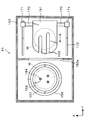
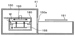
- FIG. 4 is a cross-sectional view showing an outline of the configuration of the polymer separation device 41
- FIG. 5 is a vertical cross-sectional view showing an outline of the configuration of the polymer separation device 41.
- the polymer separation apparatus 41 has a casing 150, and a temperature adjustment plate 151 for adjusting the temperature by placing the wafer W on the wafer transfer apparatus 70 side of the casing 150 is provided.
- a hot plate 152 for placing and heating the wafer W is provided.
- On the temperature adjustment plate 151 side of the housing 150 for example, a ceiling portion is opened over the entire surface, and only the heat plate 152 side is formed in a container shape having a ceiling.
- a conveyance port 150 a through which the temperature adjustment plate 151 passes is formed between the temperature adjustment plate 151 and the heat plate 152 of the housing 150.
- the hot plate 152 has a thick and substantially disk shape.
- the heat plate 152 has a horizontal upper surface, and a suction port (not shown) for sucking the wafer W, for example, is provided on the upper surface.
- the wafer W can be sucked and held on the hot plate 152 by suction from the suction port.
- an electric heater 153 as a heating mechanism is provided inside the heat plate 152, and by controlling the amount of electric power supplied to the electric heater 153 by the control unit 300 described later, The plate 152 can be controlled to a predetermined set temperature.
- the heat plate 152 has a plurality of through holes 154 penetrating in the vertical direction. Elevating pins 155 are provided in the through holes 154. The lift pins 155 can be moved up and down by a lift drive mechanism 156 such as a cylinder. The elevating pins 155 are inserted through the through holes 154 and protrude from the upper surface of the hot plate 152 to support the wafer W and elevate.
- the hot plate 152 is provided with an annular holding member 157 that holds the outer peripheral portion of the hot plate 152.
- the holding member 157 is provided with a cylindrical support ring 158 that surrounds the outer periphery of the holding member 157 and accommodates the lifting pins 155.
- the temperature control plate 151 has a substantially square flat plate shape as shown in FIG. 4, and the end surface on the heat plate 152 side is curved in an arc shape.
- two slits 160 are formed along the Y direction.
- the slit 160 is formed from the end surface of the temperature adjustment plate 151 on the heat plate 152 side to the vicinity of the center of the temperature adjustment plate 151.
- the slit 160 can prevent the temperature adjustment plate 151 from interfering with the lift pins 155 and 161.
- the lift pins 161 can be moved up and down by a lift drive mechanism 162 such as a cylinder.
- the temperature adjustment plate 151 includes a temperature adjustment member (not shown) such as a Peltier element.
- the temperature adjustment plate 151 is supported by the support arm 170 as shown in FIG.
- a drive unit 171 is attached to the support arm 170.
- the drive unit 171 is attached to a rail 172 extending in the Y direction.
- the rail 172 extends from the lower side of the temperature adjustment plate 151 to the vicinity of the lower side of the transfer port 150a.
- the temperature adjustment plate 151 can move along the rail 172 to above the heat plate 152.
- the temperature adjustment plate 151 also functions as a transfer mechanism that transfers the wafer W to and from the heat plate 152.
- a gas supply port 190 is formed near the center of the ceiling of the lid body 180, and a gas supply source 192 is connected to the gas supply port 190.
- the gas supply port 190 is provided with a supply nozzle 193 formed in a substantially disk shape.
- a supply port (not shown) is formed in the outer peripheral portion of the supply nozzle 193, and a predetermined gas or vapor supplied from the gas supply source 192 can be supplied radially in the diameter direction of the wafer.
- the hydrophilic polymer and the hydrophobic polymer of the block copolymer applied on the wafer W by the block copolymer coating apparatus 35 after heat-treating the wafer W are treated.
- a non-oxidizing gas that is not oxidized and a solvent used for solvent annealing when phase-separating the block copolymer into a hydrophilic polymer and a hydrophobic polymer are supplied.
- the lid 180 is formed to be movable up and down by an elevator mechanism (not shown). For example, as shown in FIG. 5, the lid 180 is lowered and the lower end surface of the lid 180 is brought into contact with the upper surface of the support ring 158. By doing so, the space surrounded by the holding member 157, the support ring 158, the heat plate 152, and the lid 180 can be made almost airtight. Accordingly, a predetermined gas or vapor (hereinafter, the predetermined gas or vapor may be collectively referred to as “processing gas”) is supplied from the gas supply source 192 with the lid 180 in contact with the support ring 158. As a result, the wafer W on the hot plate 152 can be covered with the atmosphere of the processing gas with the minimum processing gas.
- processing gas a predetermined gas or vapor
- the holding member 157, the support ring 158, the hot plate 152, and the lid body 180 function as a processing container capable of sealing the inside.
- an exhaust port (not shown) is formed on the upper surface of the holding member 157 so that the processing gas supplied from the gas supply source 192 can be exhausted.
- the configuration of the post-phase separation heat treatment apparatus 44 is the same as that of the polymer separation apparatus 41, and the configuration of the heat treatment apparatus 40 is also the polymer separation apparatus 41 except that the gas supply port 190 is not formed in the lid 180. It has the same composition as.
- the substrate processing system 1 described above is provided with a control unit 300 as shown in FIG.
- the control unit 300 is a computer, for example, and has a program storage unit (not shown).
- the program storage unit stores a program for controlling the processing of the wafer W in the substrate processing system 1.
- the program storage unit also stores a program for controlling the operation of driving systems such as the above-described various processing apparatuses and transfer apparatuses to realize a peeling process described later in the substrate processing system 1.
- the program is recorded on a computer-readable storage medium such as a computer-readable hard disk (HD), flexible disk (FD), compact disk (CD), magnetic optical desk (MO), or memory card. Or installed in the control unit 300 from the storage medium.
- HD computer-readable hard disk
- FD flexible disk
- CD compact disk
- MO magnetic optical desk
- FIG. 6 is a flowchart showing an example of main steps of such wafer processing.
- a cassette C containing a plurality of wafers W is carried into the cassette station 10 of the coating and developing treatment apparatus 2 and placed on a predetermined cassette placing plate 21. Thereafter, the wafers W in the cassette C are sequentially taken out by the wafer transfer device 23 and transferred to the transfer device 53 of the processing station 11.
- the wafer W is transferred to the heat treatment apparatus 40 by the wafer transfer apparatus 70 and the temperature is adjusted. Thereafter, the wafer W is transferred to the antireflection film forming apparatus 32 by the wafer transfer apparatus 70, and an antireflection film 400 is formed on the wafer W as shown in FIG. 7 (step S1 in FIG. 6). Thereafter, the wafer W is transferred to the heat treatment apparatus 40, heated, and the temperature is adjusted.
- the wafer W is transferred to the delivery device 54 by the wafer transfer device 100. Thereafter, the wafer W is transferred to the adhesion device 42 by the wafer transfer device 70 and subjected to an adhesion process. Thereafter, the wafer W is transferred to the resist coating device 34 by the wafer transfer device 70, and a resist solution is applied onto the antireflection film 400 of the wafer W to form a resist film 401. Thereafter, the wafer W is transferred to the heat treatment apparatus 40 by the wafer transfer apparatus 70 and pre-baked. Thereafter, the wafer W is transferred to the delivery device 55 by the wafer transfer device 70.
- the wafer W is transferred to the peripheral exposure device 43 by the wafer transfer device 70 and subjected to peripheral exposure processing. Thereafter, the wafer W is transferred to the delivery device 56 by the wafer transfer device 70.
- the wafer W is transferred to the transfer device 52 by the wafer transfer device 100 and transferred to the transfer device 62 by the shuttle transfer device 80.
- the wafer W is transferred to the exposure apparatus 12 by the wafer transfer apparatus 110 of the interface station 13 and subjected to exposure processing.
- the wafer W is transferred from the exposure apparatus 12 to the delivery apparatus 60 by the wafer transfer apparatus 110. Thereafter, the wafer W is transferred to the heat treatment apparatus 40 by the wafer transfer apparatus 70 and subjected to post-exposure baking. Thereafter, the wafer W is transferred to the developing device 30 by the wafer transfer device 70 and developed. After the development is completed, the wafer W is transferred to the heat treatment apparatus 40 by the wafer transfer apparatus 70 and subjected to a post-bake process. Thus, a predetermined resist pattern 402 is formed on the wafer W as shown in FIG. 8 (step S2 in FIG. 6).
- the resist pattern 402 is a so-called line-and-space resist pattern having a straight line portion 402a and a straight space portion 402b in plan view.
- the wafer W on which the resist pattern 402 is formed is transferred to the processing liquid supply device 33 by the wafer transfer device 70.
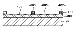
- a polystyrene solution is supplied to the resist pattern 402 on the wafer W, and a polystyrene film 403 is formed on the surface of the resist pattern 402 and the wafer W as shown in FIG. 9 (step S3 in FIG. 6). ).
- the wafer W is transferred to the heat treatment apparatus 40 by the wafer transfer apparatus 70 and subjected to heat treatment.
- the wafer W is transferred to the block copolymer coating device 35 by the wafer transfer device 70.
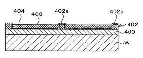
- the block copolymer supply nozzle 142 is moved from one end of the wafer W to the other end by the nozzle driving unit 143, and as shown in FIG. A block copolymer 404 is applied to the entire surface (step S4 in FIG. 6).
- the wafer W is transferred to the heat treatment apparatus 40 by the wafer transfer apparatus 70 and subjected to heat treatment.
- the temperature of the heat treatment is equal to or higher than the volatilization temperature of the solvent used to make the block copolymer 404 into a solution.
- the heptane which is a solvent volatilizes from the block copolymer 404 on the wafer W, and heptane is removed from the block copolymer 404 (step S5 in FIG. 6).
- the block copolymer 404 is gradually phase-separated into a hydrophilic polymer and a hydrophobic polymer.
- block copolymer 404 applied by the block copolymer coating device 35 is not flat due to the influence of the shape of the resist pattern 402 as shown in FIG.
- the block copolymer 404 is fluidized, and the block copolymer 404 is flattened, for example, as shown in FIG.
- the wafer W is transferred to the polymer separation device 41 by the wafer transfer device 70, and the wafer W is first delivered to the temperature adjustment plate 151 as shown in FIG.
- the temperature adjustment plate 151 is moved upward through the conveyance port 150 a.
- the lid 180 stands by above the hot plate 152 so that the hot plate 152 can pass below the lid 180.
- the hot plate 152 is set in advance to a predetermined temperature.
- the elevating pins 155 are raised and the wafer W is transferred to the elevating pins 155, and then the temperature adjustment plate 151 is retracted from below the lid 180. Thereafter, the lid body 180 is lowered, and the lower end surface of the lid body 180 and the upper surface of the support ring 158 come into contact with each other. Thereafter, another solvent is supplied from the supply nozzle 193 as a processing gas. The space surrounded by the lid 180 and the heat plate 152 is gradually replaced with the processing gas. In parallel with the lowering of the lid body 180, as shown in FIG. 15, the elevating pins 155 are lowered, the wafer W is placed on the hot plate 152, and solvent annealing is performed (step S6 in FIG. 6).
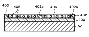
- annealing is performed at a predetermined temperature for a predetermined period under a predetermined solvent concentration, so that the hydrophobic polymer 406 is formed at the interface with the polystyrene film 403 on the wafer W as shown in FIG.
- the hydrophilic polymer 405 is phase-separated into a circular shape extending in the horizontal direction inside 406.
- the solvent supplied here is toluene or chloroform, for example.
- the predetermined temperature in the solvent annealing is a temperature at which toluene or chloroform as a solvent easily penetrates into the block copolymer 404 and is lower than the volatilization temperature of toluene or chloroform. ) To 50 ° C.
- each device operates in the reverse order of FIGS. 12 to 15, so that the wafer W is delivered to the temperature adjustment plate 151. Thereafter, the wafer W is cooled by the temperature adjustment plate 151 for a predetermined time to adjust the temperature, and the processing in the polymer separation device 41 is completed.
- step S8 the reason for using another solvent (toluene, chloroform) different from the solvent (heptane) that turns the block copolymer 404 into a solution, and the block copolymer 404 before the solvent annealing.
- the reason for volatilizing the heptane contained in is described.
- the solvent for making the block copolymer 404 into a solution it is preferable to use a solvent having high solubility for both the hydrophilic polymer and the hydrophobic polymer constituting the block copolymer.
- the solvent having such solubility the above-mentioned toluene and chloroform are applicable, but these solvents are difficult to handle.
- the volatile component does not leak to the outside.
- the solvent annealing for phase separation of the block copolymer 404 it is preferable to use a solvent having high solubility in the hydrophilic polymer 405 and the hydrophobic polymer 406. Then, the solvent annealing is performed in an airtight state by the lid body 180 as described above, and a new large-scale sealed container is not required for the external leakage of the volatile component of the solvent. As such, toluene or chloroform is used.
- the proportion of polystyrene as the hydrophobic polymer 406 is as high as 80% to 60% as in this embodiment, it is more preferable to use toluene having high polystyrene solubility.
- the size of the pattern formed by the block copolymer 404 is proportional to the value of the ⁇ (chi) parameter, which is an interaction parameter between the hydrophilic polymer 405 and the hydrophobic polymer 406 that are macromolecules constituting the block copolymer 404. And change.
- This ⁇ parameter is proportional to the blending ratio of the hydrophilic polymer 405 and the hydrophobic polymer 406, but the block copolymer 404 is in a solution state, that is, the compound of the hydrophilic polymer 405 and the hydrophobic polymer 406 is dissolved by a solvent.
- ⁇ wet which is the ⁇ parameter in the state of being present is expressed as the following equation (1).
- ⁇ wet ⁇ dry (1-f s ) (1)
- ⁇ dry is a ⁇ parameter in a dry state, that is, a state where the solvent is evaporated from the block copolymer 404
- f s is a concentration of the solvent contained in the block copolymer 404.
- the present inventors have intensively investigated, and in solvent annealing, when a solvent different from heptane, which is a solvent for making the block copolymer 404 into solution, is used, due to the interaction of both solvents, etc. It has been confirmed that there is some influence on the diffusion of the polymer, and that the pattern of the polymer after phase separation varies. This is because a plurality of solvents are mixed in the block copolymer 404, the value of ⁇ wet changes locally, or the phase separation of the block copolymer 404 is affected by the compatibility of the solvents. It is possible to do.
- the solvent (heptane) is first removed from the block copolymer 404 in the heat treatment in step S5.
- solvent annealing of process S8 a solvent is not mixed and the block copolymer 404 can be appropriately phase-separated with a desired solvent.
- the solvent concentration that is, the value of ⁇ wet can be appropriately controlled, and a pattern having a desired dimension can be obtained by the hydrophilic polymer 405 and the hydrophobic polymer 406.
- the solvent supplied here is, for example, toluene or chloroform.
- the wafer W is transferred to the heat treatment apparatus 44 after phase separation.
- the wafer W is heated at a temperature equal to or higher than the volatilization temperature of the solvent used in the solvent annealing in step S6, and the solvent is removed from the hydrophilic polymer 405 and the hydrophobic polymer 406 after the phase separation.
- Step S7 in FIG. 6 After the solvent annealing in the step S8, the solvent remains in the film of the hydrophilic polymer 405 and the hydrophobic polymer 406.
- the residual solvent causes the hydrophilic polymer 405 and the hydrophobic polymer 406 to remain. The density of the film is reduced.
- step S7 the solvent is removed by performing the heat treatment after the phase separation, the film density is improved, and the etching resistance is improved.
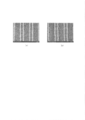
- FIG. 17A shows a pattern of the hydrophilic polymer 405 and the hydrophobic polymer 406 when the heat treatment after the phase separation is not performed
- FIG. 17B shows the hydrophilicity when the heat treatment is performed after the phase separation. This is a pattern of the conductive polymer 405 and the hydrophobic polymer 406.
- FIG. 17 (a) there are many cracked patterns in the pattern, whereas in FIG.
- the heating method is not limited to the heating by the hot plate 152, and may be, for example, by radiant heat using a lamp heater or the like.
- the wafer W is transferred to the cleaning device 31 and an organic solvent is supplied onto the wafer W. Thereby, the hydrophilic polymer 405 formed in a layer on the atmosphere side is removed.
- the wafer W is transferred to the delivery device 50 by the wafer transfer device 70, and then transferred to the cassette C of the predetermined cassette mounting plate 21 by the wafer transfer device 23 of the cassette station 10.
- the cassette C is transferred to an etching processing apparatus provided outside the substrate processing system 1, and the hydrophobic polymer 406 is selectively removed.
- the processing target film on the wafer W is etched using the hydrophilic polymer 405 as a mask.
- a predetermined pattern is formed on the film to be processed (step S8 in FIG. 6).
- an RIE (Reactive Ion Etching) apparatus is used as the etching processing apparatus. That is, in the etching processing apparatus, dry etching for etching a film to be processed such as a hydrophilic polymer or an antireflection film is performed by a reactive gas (etching gas), ions, or radicals.
- hydrophilic polymer 405 and the resist pattern 402 are removed, and a series of wafer processing ends.
- the block copolymer 404 is first heat-treated at a temperature equal to or higher than the volatilization temperature of the solvent contained in the block copolymer 404 in step S7. Remove the solvent from 404. Thereafter, the block copolymer 404 is solvent annealed in a solvent atmosphere different from the solvent removed in step S8. By this solvent annealing, other solvent penetrates into the block copolymer 404 on the wafer W, but at this point, the solvent already contained in the block copolymer 404 at the time of the coating treatment has been removed. The solvent and other solvents are not mixed.
- the block copolymer can be favorably phase-separated into the hydrophilic polymer 405 and the hydrophobic polymer 406 in the solvent annealing.
- a predetermined pattern can be appropriately formed on the wafer W in the wafer processing using the block copolymer 404 including the hydrophilic polymer 405 and the hydrophobic polymer 406.
- the fluidity of the block copolymer 404 is improved so that the hydrophilic polymer 405 and the hydrophobic polymer 406 are separated.
- a disordered state is preferable, it is difficult to heat the disordered state from the viewpoint of heat resistance of the hydrophilic polymer 405 and the hydrophobic polymer 406.
- annealing can be performed in a solvent atmosphere, and the solvent concentration in the block copolymer 404 can be made almost disordered by setting the solvent concentration to a predetermined value or more. Can be formed.
- the solvent annealing in step S8 is performed at 23 ° C. (normal temperature) to 50 ° C., which is lower than the volatilization temperature of toluene or chloroform, but the block copolymer 404 is prevented from being oxidized.
- the temperature of the wafer W in the solvent annealing may be any temperature as long as it is 150 ° C. or less.
- the solvent concentration in the block copolymer 404 can be adjusted by changing the solvent concentration, annealing time, and annealing temperature.
- the solubility of the solvent with respect to the temperature changes most markedly with temperature. Therefore, in adjusting the concentration of the solvent in the block copolymer 404 in the solvent annealing in the step S8, it is preferable to adjust the temperature of the hot plate 152 while keeping the concentration of the solvent supplied from the gas supply source constant, for example. .
- the block copolymer 404 does not properly phase-separate into the hydrophilic polymer 405 and the hydrophobic polymer 406. It is preferable to adjust the concentration of the solvent in the film of the block copolymer 404 to be a predetermined value or less. However, from the viewpoint that the hydrophilic polymer 405 and the hydrophobic polymer 406 are diffused and the pattern is properly arranged, it is preferable that the value of ⁇ wet is large. Therefore, in the film of the block copolymer 404 in the solvent annealing, It is preferable to maintain the concentration of the solvent as high as possible.
- the solvent annealing is performed on the hot plate 152 inside the lid 180.
- the polymer separation apparatus Solvent annealing may be performed by the polymer separation device 41 in which the arrangement of the 41 hot plate 152 and the temperature control plate 151 is exchanged. In such a case, the slit 160 is formed in the hot plate 152.
- the present invention is not limited to such examples. It is obvious for those skilled in the art that various changes or modifications can be conceived within the scope of the idea described in the claims, and these are naturally within the technical scope of the present invention. It is understood.
- the present invention is not limited to this example and can take various forms.
- the present invention can also be applied to a case where the substrate is another substrate such as an FPD (flat panel display) other than a wafer or a mask reticle for a photomask.
- FPD flat panel display
- the present invention is useful when a substrate is treated with a block copolymer containing, for example, a hydrophilic polymer having hydrophilicity and a hydrophobic polymer having hydrophobicity.
Landscapes
- Photosensitive Polymer And Photoresist Processing (AREA)
- Exposure Of Semiconductors, Excluding Electron Or Ion Beam Exposure (AREA)
Abstract
第1のポリマーと第2のポリマーとを含むブロック共重合体を用いて、基板を処理する基板処理方法は、パターンが形成された基板上にブロック共重合体を塗布し、ブロック共重合体塗布後の基板を、ブロック共重合体に含まれる溶剤の揮発温度以上で加熱処理して当該ブロック共重合体から溶剤を除去し、溶剤除去後の基板を、当該除去した溶剤とは異なる他の溶剤の雰囲気内でアニール処理して、ブロック共重合体を第1のポリマーと第2のポリマーに相分離させ、他の溶剤の揮発温度よりも低い温度で当該アニール処理が行われる。
Description
(関連出願の相互参照)
本願は、2014年2月25日に日本国に出願された特願2014-034658号に基づき、優先権を主張し、その内容をここに援用する。
本願は、2014年2月25日に日本国に出願された特願2014-034658号に基づき、優先権を主張し、その内容をここに援用する。
本発明は、親水性(極性)を有する親水性(有極性)ポリマーと疎水性を有する(極性を有さない)疎水性(無極性)ポリマーとを含むブロック共重合体を用いた基板処理方法、コンピュータ記憶媒体及び基板処理システムに関する。
例えば半導体デバイスの製造工程では、例えば半導体ウェハ(以下、「ウェハ」という。)上にレジスト液を塗布してレジスト膜を形成するレジスト塗布処理、当該レジスト膜に所定のパターンを露光する露光処理、露光されたレジスト膜を現像する現像処理などを順次行うフォトリソグラフィー処理が行われ、ウェハ上に所定のレジストパターンが形成される。そして、このレジストパターンをマスクとして、ウェハ上の被処理膜のエッチング処理が行われ、その後レジスト膜の除去処理などが行われて、被処理膜に所定のパターンが形成される。
ところで、近年、半導体デバイスのさらなる高集積化を図るため、上述した被処理膜のパターンの微細化が求められている。このため、レジストパターンの微細化が進められており、例えばフォトリソグラフィー処理における露光処理の光を短波長化することが進められている。しかしながら、露光光源の短波長化には技術的、コスト的な限界があり、光の短波長化を進める方法のみでは、例えば数ナノメートルオーダーの微細なレジストパターンを形成するのが困難な状況にある。
そこで、親水性と疎水性の2種類のブロック鎖(ポリマー)から構成されたブロック共重合体を用いたウェハ処理方法が提案されている(特許文献1)。かかる方法では、先ず、ウェハ上に2種類のポリマーに対して中間の親和性を有する中性層を形成し、当該中性層上に例えばレジストによりガイドパターンを形成する。その後、中性層上にブロック共重合体を塗布し、当該ブロック共重合体に対して加熱処理や溶剤雰囲気中でのアニール処理を行うことで親水性ポリマーと疎水性ポリマーに相分離させる。その後、いずれか一方のポリマーを、例えばエッチング等により選択的に除去することで、ウェハ上に他方のポリマーにより微細なパターンが形成される。そして、このポリマーのパターンをマスクとして被処理膜のエッチング処理が行われ、被処理膜に所定のパターンが形成される。
しかしながら本発明者らによれば、溶剤雰囲気中でのアニール処理によりブロック共重合体を相分離させると、相分離後のポリマーによるパターンにばらつきが生じる場合があることが確認されている。
この点について本発明者らが鋭意検討したところ、溶剤雰囲気中でのアニール処理に用いられる溶剤と、ブロック共重合体をウェハに塗布するために、当該ブロック共重合体を溶液状にするために用いられる溶剤とが異なっていることが原因であるとの知見を得た。即ち、ブロック共重合体を溶液状にするための溶剤は、ウェハへの均一な塗布を目的としてウェハとの濡れ性等を考慮して選定され、その一方、溶剤雰囲気中でのアニール処理に用いられる溶剤は、ブロック共重合体の相分離の促進を考慮して選定される。そうすると、溶剤雰囲気中でのアニール処理において、両方の溶剤の相互作用等によりポリマーの拡散に何らかの影響を与え、相分離後のポリマーのパターンにばらつきが生じるものと推察される。
そこで本発明者らがさらに検討したところ、溶剤雰囲気中でのアニール処理を行う前に、ブロック共重合体に含まれている塗布処理用の溶剤を除去し、溶剤雰囲気中でのアニール処理において溶剤が混合しないようにすれば、ポリマーによるパターンのばらつきを抑えられるとの知見を得た。
本発明は、かかる点に鑑みてなされたものであり、親水性ポリマーと疎水性ポリマーとを含むブロック共重合体を用いた基板処理において、基板上に所定のパターンを適切に形成することを目的とする。
前記の目的を達成するため、本発明は、第1のポリマーと第2のポリマーとを含むブロック共重合体を用いて、基板を処理する基板処理方法であって、
所定のパターンが形成された基板上に前記ブロック共重合体を塗布するブロック共重合体塗布工程と、
前記ブロック共重合体塗布後の基板を、前記ブロック共重合体に含まれる溶剤の揮発温度以上で加熱処理して当該ブロック共重合から溶剤を除去する溶剤除去工程と、
前記溶剤除去後の基板を、前記除去した溶剤とは異なる他の溶剤の雰囲気内でアニール処理して、前記ブロック共重合体を前記第1のポリマーと前記第2のポリマーに相分離させるポリマー分離工程と、を有し、
前記ポリマー分離工程におけるアニール処理は、前記他の溶剤の揮発温度よりも低い温度で行われる。
所定のパターンが形成された基板上に前記ブロック共重合体を塗布するブロック共重合体塗布工程と、
前記ブロック共重合体塗布後の基板を、前記ブロック共重合体に含まれる溶剤の揮発温度以上で加熱処理して当該ブロック共重合から溶剤を除去する溶剤除去工程と、
前記溶剤除去後の基板を、前記除去した溶剤とは異なる他の溶剤の雰囲気内でアニール処理して、前記ブロック共重合体を前記第1のポリマーと前記第2のポリマーに相分離させるポリマー分離工程と、を有し、
前記ポリマー分離工程におけるアニール処理は、前記他の溶剤の揮発温度よりも低い温度で行われる。
本発明によれば、先ずブロック共重合体が塗布された基板を当該ブロック共重合体に含まれる溶剤の揮発温度以上で加熱処理することで、ブロック共重合体から溶剤を除去し、その後、除去した溶剤とは異なる他の溶剤雰囲気でブロック共重合体を、アニール処理する。このアニール処理により、基板上のブロック共重合体の内部に他の溶剤が浸透するがこの時点では既に塗布処理時のブロック共重合体に含まれていた溶剤が除去されているので、当該溶剤と他の溶剤とが混合することがない。そして、他の溶剤として、ブロック共重合体の相分離を促進させる溶剤を用いることで、アニール処理においてブロック共重合体を第1のポリマーと第2のポリマーに良好に相分離させることができる。その結果、第1のポリマーと第2のポリマーとを含むブロック共重合体を用いた基板処理において、基板上に所定のパターンを適切に形成することができる。
別な観点による本発明は、前記基板処理方法を基板処理システムによって実行させるために、当該基板処理システムを制御する制御部のコンピュータ上で動作するプログラムを格納した読み取り可能なコンピュータ記憶媒体である。
さらに別な観点による本発明は、第1のポリマーと第2のポリマーとを含むブロック共重合体を用いて、基板を処理する基板処理システムであって、所定のパターンが形成された基板上に前記ブロック共重合体を塗布するブロック共重合体塗布装置と、前記ブロック共重合体塗布後の基板を、前記ブロック共重合体に含まれる溶剤の揮発温度以上で加熱処理して前記ブロック共重合から溶剤を除去する溶剤除去装置と、前記溶剤除去後の基板を、前記除去した溶剤とは異なる他の溶剤の雰囲気内でアニール処理して、前記ブロック共重合体を前記第1のポリマーと前記第2のポリマーに相分離させるポリマー分離装置と、前記ポリマー分離装置でのアニール処理を、前記他の溶剤の揮発温度よりも低い温度で行うように前記ポリマー分離装置を制御する制御装置と、を有する。
本発明によれば、親水性ポリマーと疎水性ポリマーとを含むブロック共重合体を用いた基板処理において、基板上に所定のパターンを適切に形成することができる。
以下、本発明の実施の形態について説明する。図1は、本実施の形態にかかる基板処理システム1の構成の概略を示す説明図である。図2及び図3は、基板処理システム1の内部構成の概略を示す正面図及び背面図である。
基板処理システム1は、図1に示すように複数枚のウェハWを収容したカセットCが搬入出されるカセットステーション10と、ウェハWに所定の処理を施す複数の各種処理装置を備えた処理ステーション11と、処理ステーション11に隣接する露光装置12との間でウェハWの受け渡しを行うインターフェイスステーション13とを一体に接続した構成を有している。
カセットステーション10には、カセット載置台20が設けられている。カセット載置台20には、基板処理システム1の外部に対してカセットCを搬入出する際に、カセットCを載置する、例えば4つのカセット載置板21が設けられている。
カセットステーション10には、図1に示すようにX方向に延びる搬送路22上を移動自在なウェハ搬送装置23が設けられている。ウェハ搬送装置23は、上下方向及び鉛直軸周り(θ方向)にも移動自在であり、各カセット載置板21上のカセットCと、後述する処理ステーション11の第3のブロックG3の受け渡し装置との間でウェハWを搬送できる。
処理ステーション11には、各種装置を備えた複数例えば4つのブロックG1、G2、G3、G4が設けられている。例えば処理ステーション11の正面側(図1のX方向負方向側)には、第1のブロックG1が設けられ、処理ステーション11の背面側(図1のX方向正方向側)には、第2のブロックG2が設けられている。また、処理ステーション11のカセットステーション10側(図1のY方向負方向側)には、第3のブロックG3が設けられ、処理ステーション11のインターフェイスステーション13側(図1のY方向正方向側)には、第4のブロックG4が設けられている。
例えば第1のブロックG1には、図2に示すように複数の液処理装置、例えばウェハWを現像処理する現像装置30、ウェハW上に有機溶剤を塗布してウェハWを洗浄する洗浄装置31、ウェハW上に反射防止膜を形成する反射防止膜形成装置32、ウェハW上に処理液を塗布する処理液供給装置33、ウェハW上にレジスト液を塗布してレジスト膜を形成するレジスト塗布装置34、ウェハW上にブロック共重合体を塗布するブロック共重合体塗布装置35が下から順に重ねられている。
例えば現像装置30、洗浄装置31、反射防止膜形成装置32、処理液供給装置33、レジスト塗布装置34、ブロック共重合体塗布装置35は、それぞれ水平方向に3つ並べて配置されている。なお、これら現像装置30、洗浄装置31、反射防止膜形成装置32、処理液供給装置33、レジスト塗布装置34、ブロック共重合体塗布装置35の数や配置は、任意に選択できる。
これら現像装置30、洗浄装置31、反射防止膜形成装置32、処理液供給装置33、レジスト塗布装置34、ブロック共重合体塗布装置35では、例えばウェハW上に所定の塗布液を塗布するスピンコーティングが行われる。スピンコーティングでは、例えば塗布ノズルからウェハW上に塗布液を吐出すると共に、ウェハWを回転させて、塗布液をウェハWの表面に拡散させる。これら液処理装置の構成については後述する。
なお、ブロック共重合体塗布装置35でウェハW上に塗布されるブロック共重合体は、第1のポリマーと第2のポリマーとを有する。第1のポリマーとしては、極性を有する(親水性)ポリマーである親水性ポリマーが用いられ、第2のポリマーとしては、極性を有しない(疎水性)ポリマーである疎水性ポリマーが用いられる。本実施の形態では、親水性(極性)ポリマーとして例えばポリジメチルシロキサン(PDMS)が用いられ、疎水性(非極性)ポリマーとしては例えばポリスチレン(PS)が用いられる。また、ブロック共重合体における親水性ポリマーの分子量の比率は20%~40%であり、ブロック共重合体における疎水性ポリマーの分子量の比率は80%~60%である。そして、ブロック共重合体は、親水性ポリマーと疎水性ポリマーが、直線的に化合した高分子であり、これら親水性ポリマーと疎水性ポリマーの化合物を溶剤によりにより溶液状としたものである。なお、この溶剤には、例えばヘプタンなどが用いられる。
また、処理液供給装置33で用いられる処理液は、例えばポリスチレンの溶液であり、例えばレジストパターン形成後のウェハWに対してポリスチレンを供給することで、レジストパターンの表面にポリスチレンの膜が形成される。
例えば第2のブロックG2には、図3に示すようにウェハWの加熱処理を行う熱処理装置40、ブロック共重合体塗布装置35でウェハW上に塗布されたブロック共重合体を溶剤雰囲気でアニールすることで親水性ポリマーと疎水性ポリマーに相分離させるポリマー分離装置41、ウェハWを疎水化処理するアドヒージョン装置42、ウェハWの外周部を露光する周辺露光装置43、ポリマー相分離後のウェハWを加熱処理して溶剤を除去する相分離後熱処理装置44が上下方向と水平方向に並べて設けられている。熱処理装置40は、ウェハWを載置して加熱する熱板と、ウェハWを載置して温度調節する温度調節板を有し、加熱処理と温度調節処理の両方を行うことができる。なお、ポリマー分離装置41もウェハWに対して熱処理を施す装置であり、その構成は概ね熱処理装置40と同様である。このポリマー分離装置41の構成については後述する。また、熱処理装置40、ポリマー分離装置41、アドヒージョン装置42、周辺露光装置43、相分離後熱処理装置44の数や配置は、任意に選択できる。
例えば第3のブロックG3には、複数の受け渡し装置50、51、52、53、54、55、56が下から順に設けられている。また、第4のブロックG4には、複数の受け渡し装置60、61、62が下から順に設けられている。
図1に示すように第1のブロックG1~第4のブロックG4に囲まれた領域には、ウェハ搬送領域Dが形成されている。ウェハ搬送領域Dには、例えばY方向、X方向、θ方向及び上下方向に移動自在な搬送アームを有する、ウェハ搬送装置70が複数配置されている。ウェハ搬送装置70は、ウェハ搬送領域D内を移動し、周囲の第1のブロックG1、第2のブロックG2、第3のブロックG3及び第4のブロックG4内の所定の装置にウェハWを搬送できる。
また、ウェハ搬送領域Dには、第3のブロックG3と第4のブロックG4との間で直線的にウェハWを搬送するシャトル搬送装置80が設けられている。
シャトル搬送装置80は、例えばY方向に直線的に移動自在になっている。シャトル搬送装置80は、ウェハWを支持した状態でY方向に移動し、第3のブロックG3の受け渡し装置52と第4のブロックG4の受け渡し装置62との間でウェハWを搬送できる。
図1に示すように第3のブロックG3のX方向正方向側の隣には、ウェハ搬送装置100が設けられている。ウェハ搬送装置100は、例えばX方向、θ方向及び上下方向に移動自在な搬送アームを有している。ウェハ搬送装置100は、ウェハWを支持した状態で上下に移動して、第3のブロックG3内の各受け渡し装置にウェハWを搬送できる。
インターフェイスステーション13には、ウェハ搬送装置110と受け渡し装置111が設けられている。ウェハ搬送装置110は、例えばY方向、θ方向及び上下方向に移動自在な搬送アームを有している。ウェハ搬送装置110は、例えば搬送アームにウェハWを支持して、第4のブロックG4内の各受け渡し装置、受け渡し装置111及び露光装置12との間でウェハWを搬送できる。
次に、上述したポリマー分離装置41の構成について説明する。図4は、ポリマー分離装置41の構成の概略を示す横断面図であり、図5は、ポリマー分離装置41の構成の概略を示す縦断面図である。
例えばポリマー分離装置41は、筐体150を有し、筐体150のウェハ搬送装置70側にはウェハWを載置して温度調節する温度調節板151が設けられている。温度調節板151を挟んでウェハ搬送装置70側と反対の側には、ウェハWを載置して加熱する熱板152が設けられている。筐体150の温度調節板151側は、例えば天井部が全面にわたって開口しており、熱板152側のみが天井を有する容器状に形成されている。筐体150の温度調節板151と熱板152との間には温度調節板151が通過する搬送口150aが形成されている。
熱板152は、厚みのある略円盤形状を有している。熱板152は、水平な上面を有し、当該上面には、例えばウェハWを吸引する吸引口(図示せず)が設けられている。この吸引口からの吸引により、ウェハWを熱板152上に吸着保持できる。
熱板152の内部には、図5に示すように、加熱機構としての電気ヒータ153が設けられており、後述する制御部300により電気ヒータ153への電力の供給量を制御することにより、熱板152を所定の設定温度に制御することができる。
熱板152には、上下方向に貫通する複数の貫通孔154が形成されている。貫通孔154には、昇降ピン155が設けられている。昇降ピン155は、シリンダなどの昇降駆動機構156によって上下動できる。昇降ピン155は、貫通孔154内を挿通して熱板152の上面に突出し、ウェハWを支持して昇降できる。
熱板152には、当該熱板152の外周部を保持する環状の保持部材157が設けられている。保持部材157には、当該保持部材157の外周を囲み、昇降ピン155を収容する筒状のサポートリング158が設けられている。
温度調節板151は、図4に示すように略方形の平板形状を有し、熱板152側の端面が円弧状に湾曲している。温度調節板151には、Y方向に沿った2本のスリット160が形成されている。スリット160は、温度調節板151における熱板152側の端面から温度調節板151の中央部付近まで形成されている。このスリット160により、温度調節板151が、昇降ピン155、161と干渉するのを防止できる。昇降ピン161は、シリンダなどの昇降駆動機構162によって上下動できる。また、温度調節板151には、例えばペルチェ素子などの温度調節部材(図示せず)が内蔵されている。
温度調節板151は、図4に示すように支持アーム170に支持されている。支持アーム170には、駆動部171が取り付けられている。駆動部171は、Y方向に延伸するレール172に取り付けられている。レール172は、温度調節板151の下方から搬送口150aの下方近傍まで延伸している。この駆動部171により、温度調節板151は、レール172に沿って熱板152の上方まで移動可能になっている。このような構成により、温度調節板151は熱板152との間でウェハWの受け渡しを行う搬送機構としても機能する。
熱板152の上方には、例えばサポートリング158と同じ径を有する筒状の蓋体180が設けられている。蓋体180の天井部であって、中央部近傍にはガス供給口190が形成されており、ガス供給口190にはガス供給源192が接続されている。ガス供給口190には略円盤状に形成された供給ノズル193が設けられている。供給ノズル193の外周部には、図示しない供給口が形成されており、ガス供給源192から供給された所定のガスや蒸気をウェハの直径方向に放射状に供給できる。なお、本実施の形態では、ガス供給源192からは、例えばウェハWを熱処理してブロック共重合体塗布装置35でウェハW上に塗布されたブロック共重合体の親水性ポリマーと疎水性ポリマーを酸化させない非酸化性ガス、及びブロック共重合体を親水性ポリマーと疎水性ポリマーに相分離させる際の溶剤アニールに用いられる溶剤が供給される。
蓋体180は図示しない昇降機構により昇降自在に形成されており、例えば、図5に示すように、蓋体180を下降させて、当該蓋体180の下端面をサポートリング158の上面に当接させることで、保持部材157、サポートリング158及び熱板152と蓋体180とで囲まれる空間をほぼ気密な状態とすることができる。したがって、蓋体180をサポートリング158に当接させた状態でガス供給源192から所定のガスや蒸気(以下、所定のガスや蒸気を総称して「処理ガス」という場合がある)を供給することで、最小限の処理ガスで熱板152上のウェハWを処理ガスの雰囲気で覆うことができる。かかる場合、保持部材157、サポートリング158及び熱板152と蓋体180は、内部を密閉可能な処理容器として機能する。なお、例えば保持部材157の上面には、図示しない排気口が形成されており、ガス供給源192から供給された処理ガスを排気することができる。
なお、相分離後熱処理装置44の構成はポリマー分離装置41の構成と同様であり、熱処理装置40の構成についても蓋体180にガス供給口190が形成されていない点を除いてポリマー分離装置41と同様の構成を有している。
以上の基板処理システム1には、図1に示すように制御部300が設けられている。制御部300は、例えばコンピュータであり、プログラム格納部(図示せず)を有している。プログラム格納部には、基板処理システム1におけるウェハWの処理を制御するプログラムが格納されている。また、プログラム格納部には、上述の各種処理装置や搬送装置などの駆動系の動作を制御して、基板処理システム1における後述の剥離処理を実現させるためのプログラムも格納されている。なお、前記プログラムは、例えばコンピュータ読み取り可能なハードディスク(HD)、フレキシブルディスク(FD)、コンパクトディスク(CD)、マグネットオプティカルデスク(MO)、メモリーカードなどのコンピュータに読み取り可能な記憶媒体に記録されていたものであって、その記憶媒体から制御部300にインストールされたものであってもよい。
次に、以上のように構成された基板処理システム1を用いて行われるウェハ処理について説明する。図6は、かかるウェハ処理の主な工程の例を示すフローチャートである。
先ず、複数のウェハWを収納したカセットCが、塗布現像処理装置2のカセットステーション10に搬入され、所定のカセット載置板21に載置される。その後、ウェハ搬送装置23によりカセットC内の各ウェハWが順次取り出され、処理ステーション11の受け渡し装置53に搬送される。
次にウェハWは、ウェハ搬送装置70によって熱処理装置40に搬送され、温度調節される。その後ウェハWは、ウェハ搬送装置70によって反射防止膜形成装置32に搬送され、図7に示すようにウェハW上に反射防止膜400が形成される(図6の工程S1)。その後ウェハWは、熱処理装置40に搬送され、加熱され、温度調節される。
次にウェハWは、ウェハ搬送装置100によって受け渡し装置54に搬送される。その後ウェハWは、ウェハ搬送装置70によってアドヒージョン装置42に搬送され、アドヒージョン処理される。その後ウェハWは、ウェハ搬送装置70によってレジスト塗布装置34に搬送され、ウェハWの反射防止膜400上にレジスト液が塗布されて、レジスト膜401が形成される。その後ウェハWは、ウェハ搬送装置70によって熱処理装置40に搬送されて、プリベーク処理される。その後ウェハWは、ウェハ搬送装置70によって受け渡し装置55に搬送される。
次にウェハWは、ウェハ搬送装置70によって周辺露光装置43に搬送され、周辺露光処理される。その後ウェハWは、ウェハ搬送装置70によって受け渡し装置56に搬送される。
次にウェハWは、ウェハ搬送装置100によって受け渡し装置52に搬送され、シャトル搬送装置80によって受け渡し装置62に搬送される。
その後ウェハWは、インターフェイスステーション13のウェハ搬送装置110によって露光装置12に搬送され、露光処理される。
次にウェハWは、ウェハ搬送装置110によって露光装置12から受け渡し装置60に搬送される。その後ウェハWは、ウェハ搬送装置70によって熱処理装置40に搬送され、露光後ベーク処理される。その後ウェハWは、ウェハ搬送装置70によって現像装置30に搬送され、現像される。現像終了後、ウェハWは、ウェハ搬送装置70によって熱処理装置40に搬送され、ポストベーク処理される。こうして、図8に示すようにウェハW上に所定のレジストパターン402が形成される(図6の工程S2)
なお、本実施の形態では、レジストパターン402は、平面視において直線状のライン部402aと直線状のスペース部402bを有し、いわゆるラインアンドスペースのレジストパターンである。
レジストパターン402が形成されたウェハWは、ウェハ搬送装置70によって処理液供給装置33に搬送される。処理液供給装置33では、ウェハW上のレジストパターン402にポリスチレンの溶液が供給され、図9に示すようにレジストパターン402及びウェハWの表面にポリスチレン膜403が形成される(図6の工程S3)。その後ウェハWは、ウェハ搬送装置70によって熱処理装置40に搬送されて、加熱処理される。その後ウェハWは、ウェハ搬送装置70によってブロック共重合体塗布装置35に搬送される。ブロック共重合体塗布装置35では、ノズル駆動部143によりブロック共重合体供給ノズル142がウェハWの一端部から他の端部へ移動し、図10に示すようにウェハWのポリスチレン膜403上の全面にブロック共重合体404が塗布される(図6の工程S4)。
次にウェハWは、ウェハ搬送装置70によって熱処理装置40に搬送されて、加熱処理される。この際、加熱処理の温度は、ブロック共重合体404を溶液状にするために用いられていた溶剤の揮発温度以上である。これにより、ウェハW上のブロック共重合体404から溶剤であるヘプタンが揮発して、ブロック共重合体404からヘプタンが除去される(図6の工程S5)。それと共に、ブロック共重合体404が徐々に親水性ポリマーと疎水性ポリマーに相分離される。また、ブロック共重合体塗布装置35で塗布されたブロック共重合体404は、例えば図10に示すように、レジストパターン402の形状の影響を受けて平坦状になっていないが、熱処理装置40での熱処理により、ブロック共重合体404が流動化して、例えば図11に示すようにブロック共重合体404が平坦状にならされる。
次にウェハWは、ウェハ搬送装置70によってポリマー分離装置41に搬送され、ウェハWは先ず図12に示すように、温度調節板151にウェハWが受け渡される。次いで、図13に示すように、搬送口150aを介して温度調節板151を熱板152の上方向に移動させる。この際、蓋体180は、当該蓋体180の下方を熱板152が通過できるように、熱板152の上方で待機している。また、熱板152は予め所定の温度に設定されている。
その後、図14に示すように昇降ピン155が上昇してウェハWが昇降ピンに155受け渡され、次いで温度調節板151が蓋体180の下方から退避する。その後、蓋体180が下降して、蓋体180の下端面とサポートリング158の上面とが当接する。その後、供給ノズル193から処理ガスとして他の溶剤が供給される。蓋体180と熱板152とで囲まれた空間内が徐々に処理ガスに置換される。蓋体180の下降と並行して、図15に示すように昇降ピン155が下降してウェハWが熱板152に載置されて溶剤アニールが行われる(図6の工程S6)。この溶剤アニールにおいて所定の溶剤濃度下において所定の期間、所定の温度でアニールされることで、図16に示すようにウェハW上のポリスチレン膜403との界面に疎水性ポリマー406が、疎水性ポリマー406の内部に親水性ポリマー405が水平方向に延伸する円形状に相分離される。なお、ここで供給される溶剤は、例えばトルエンやクロロホルムである。また、溶剤アニールにおける所定の温度は、ブロック共重合体404の内部に溶剤としてのトルエンやクロロホルムが浸透しやすく、且つトルエンやクロロホルムの揮発温度より低い温度であり、具体的には、23(常温)~50℃である。
その後、所定の時間溶剤アニールが行われると、蓋体180と昇降ピン155が上昇し、ポリマー分離装置41での熱処理が終了する。次いで、図12~図15と逆の順序で各機器が動作が動作することで、ウェハWが温度調節板151に受け渡される。その後、ウェハWが温度調節板151で所定の時間冷却されて温度調整され、ポリマー分離装置41での処理が終了する。
ここで、工程S8の溶剤アニールにおいて、ブロック共重合体404を溶液状にする溶剤(ヘプタン)とは異なる他の溶剤(トルエン、クロロホルム)を用いる理由、及び溶剤アニールの前にブロック共重合体404に含まれるヘプタンを揮発させる理由について説明する。
先ず、溶剤アニールにおいてブロック共重合体404を溶液状にする溶剤とは異なる溶剤を用いる理由について説明する。ブロック共重合体404を溶液状にする溶剤には、ブロック共重合体を構成する親水性ポリマーと疎水性ポリマーの双方に対して溶解度が高いものを用いることが好ましい。そのような溶解度の溶剤としては、上述のトルエンやクロロホルムが該当するものの、これらの溶剤は取扱いが難しいので、例えばブロック共重合体塗布装置35で塗布処理を行う場合に外部に揮発分が漏洩しないように、当該ブロック共重合体塗布装置35を大がかりな密閉容器とするなどの対策が必要となる。そのため、極力既存のブロック共重合体塗布装置35に適用可能な溶剤を用いることが好ましく、そのような溶剤としてヘプタンが選定される。
一方、ブロック共重合体404を相分離させるための溶剤アニールにおいても、親水性ポリマー405と疎水性ポリマー406に対する溶解度が高いものを用いることが好ましい。そして、溶剤アニールは、上述のように蓋体180により気密な状態で行われ、溶剤の揮発分の外部漏洩のために新たに大がかりな密閉容器を必要としないので、ポリマー分離装置41では好ましい溶剤として、トルエンやクロロホルムが用いられる。特に、本実施の形態のように、疎水性ポリマー406であるポリスチレンの比率が80%~60%と高い場合は、ポリスチレンの溶解度が高いトルエンを用いることがより好ましい。
次に、溶剤アニールの前にブロック共重合体404に含まれるヘプタンを揮発させる理由について説明する。ブロック共重合体404よるパターンの寸法は、ブロック共重合体404を構成する高分子である親水性ポリマー405と疎水性ポリマー406との間の相互作用パラメータであるχ(カイ)パラメータの値に比例して変化する。このχパラメータは、親水性ポリマー405と疎水性ポリマー406の配合比に比例するが、ブロック共重合体404が溶液の状態、即ち親水性ポリマー405と疎水性ポリマー406の化合物を溶剤により溶解させている状態におけるχパラメータであるχwetは、以下の式(1)のように表される。
χwet=χdry(1-fs) ・・・(1)
ここでχdryは乾燥状態、即ちブロック共重合体404から溶剤が蒸発した状態におけるχパラメータであり、fsはブロック共重合体404に含まれる溶剤の濃度である。
χwet=χdry(1-fs) ・・・(1)
ここでχdryは乾燥状態、即ちブロック共重合体404から溶剤が蒸発した状態におけるχパラメータであり、fsはブロック共重合体404に含まれる溶剤の濃度である。
ところが、既述のとおり、本発明者らが鋭意調査したところ、溶剤アニールにおいて、ブロック共重合体404を溶液状にする溶剤であるヘプタンと異なる溶剤を用いると、両方の溶剤の相互作用等によりポリマーの拡散に何らかの影響を与え、相分離後のポリマーのパターンにばらつきが生じることが確認されている。これは、ブロック共重合体404中に複数の溶剤が混在することで、χwetの値が局所的に変化したり、或いは溶剤同士の相性によりブロック共重合体404の相分離に影響を与えたりしたりすることが考えられる。したがって、本実施の形態では、工程S5の加熱処理において先ずブロック共重合体404から溶剤(ヘプタン)を除去する。これにより、工程S8の溶剤アニールにおいて、溶剤が混ざることが無く、ブロック共重合体404を所望の溶剤により適正に相分離させることができる。また、溶剤が混合することがないので、溶剤の濃度、即ちχwetの値を適正に制御し、親水性ポリマー405と疎水性ポリマー406により所望の寸法のパターンを得ることができる。また、工程S8の溶剤アニールにおいては、ここで供給される溶剤は、例えばトルエンやクロロホルムである。
その後、ウェハWは相分離後熱処理装置44に搬送される。相分離後熱処理装置44では、ウェハWが工程S6の溶剤アニールで用いた溶剤の揮発温度以上の温度で加熱処理され、相分離後の親水性ポリマー405及び疎水性ポリマー406から溶剤が除去される(図6の工程S7)。工程S8の溶剤アニール後には、親水性ポリマー405及び疎水性ポリマー406の膜中に溶剤が残っており、本発明者らによれば、この残留溶剤により、親水性ポリマー405及び疎水性ポリマー406の膜の密度が低下してしまう。そうすると、その後のエッチング工程においてエッチング耐性が低下し、パターン形状の悪化を引き起こす。そこで、本実施の形態では、工程S7において、相分離後の加熱処理を行うことで溶剤を除去し、膜密度を向上させてエッチング耐性の向上が図られる。図17(a)は、相分離後の加熱処理を行わない場合の親水性ポリマー405及び疎水性ポリマー406のパターンであり、図17(b)は、相分離後に加熱処理を行った場合の親水性ポリマー405及び疎水性ポリマー406のパターンである。図17(a)では、パターンにひび割れ状の模様が多数入っているのに対して、図17(b)ではそのようなひび割れはほとんど確認できず、相分離後の加熱処理により膜密度が向上していることが確認できる。なお、相分離後の加熱処理を行うにあたって、加熱方法は熱板152での加熱に限定されるものではなく、例えばランプヒータなどを用いた輻射熱によるものであってもよい。
その後、ウェハWは洗浄装置31に搬送され、ウェハW上に有機溶剤が供給される。これにより、大気側に層状に形成された親水性ポリマー405が除去される。
その後ウェハWは、ウェハ搬送装置70によって受け渡し装置50に搬送され、その後カセットステーション10のウェハ搬送装置23によって所定のカセット載置板21のカセットCに搬送される。
その後、カセットCは基板処理システム1の外部に設けられたエッチング処理装置に搬送され、疎水性ポリマー406が選択的に除去される。次いで、エッチング処理装置では親水性ポリマー405をマスクとして、ウェハW上の被処理膜がエッチング処理される。これにより、被処理膜に所定のパターンが形成される(図6の工程S8)。なお、エッチング処理装置としては、例えばRIE(Reactive Ion Eching)装置が用いられる。すなわち、エッチング処理装置では、反応性の気体(エッチングガス)やイオン、ラジカルによって、親水性ポリマーや反射防止膜といった被処理膜をエッチングするドライエッチングが行われる。
その後、親水性ポリマー405及びレジストパターン402が除去されて、一連のウェハ処理が終了する。
以上の実施の形態によれば、先ずブロック共重合体404が塗布されたウェハWを、工程S7においてブロック共重合体404に含まれる溶剤の揮発温度以上で加熱処理することで、ブロック共重合体404から溶剤を除去する。その後、工程S8において除去した溶剤とは異なる他の溶剤雰囲気でブロック共重合体404を溶剤アニールする。この溶剤アニールにより、ウェハW上のブロック共重合体404の内部に他の溶剤が浸透するがこの時点では既に塗布処理時のブロック共重合体404に含まれていた溶剤が除去されているので、当該溶剤と他の溶剤とが混合することがない。そして、他の溶剤として、ブロック共重合体の相分離に好ましいトルエンなどを用いることで、溶剤アニールにおいてブロック共重合体を親水性ポリマー405と疎水性ポリマー406に良好に相分離させることができる。その結果、親水性ポリマー405と疎水性ポリマー406とを含むブロック共重合体404を用いたウェハ処理において、ウェハW上に所定のパターンを適切に形成することができる。
また、ブロック共重合体404を親水性ポリマー405と疎水性ポリマー406に相分離させてパターンを形成する場合、ブロック共重合体404の流動性を向上させて親水性ポリマー405と疎水性ポリマー406を無秩序状態にすることが好ましいが、親水性ポリマー405と疎水性ポリマー406の耐熱性の観点から、無秩序状態まで加熱処理することは困難である。それに対して本実施の形態のように、溶剤雰囲気中でアニール処理し、ブロック共重合体404中の溶剤濃度を所定の値以上にすることでほぼ無秩序状態とすることができ、良好なパターンを形成することができる。
なお、以上の実施の形態では、工程S8の溶剤アニールをトルエンやクロロホルムの揮発温度より低い温度である23℃(常温)~50℃で行ったが、ブロック共重合体404の酸化を防止するという観点からは、溶剤アニールにおけるウェハWの温度は150℃以下なら任意の温度でよい。
以上の実施の形態にかかる溶剤アニールにおいては、溶剤の濃度、アニールの時間、アニールの温度を変化させることでブロック共重合体404中の溶剤濃度を調整することができるが、ブロック共重合体404に対する溶剤の溶解度は温度により変化が最も顕著である。したがって、工程S8の溶剤アニールにおいてブロック共重合体404中の溶剤の濃度を調整するにあたっては、例えばガス供給源から供給する溶剤の濃度を一定に保ち、熱板152の温度を調整することが好ましい。
また、上述の式(1)で示されるχwetの値が所定の値以下になると、ブロック共重合体404が親水性ポリマー405と疎水性ポリマー406に適正に相分離しなくなるので、溶剤アニールにおけるブロック共重合体404の膜中の溶剤濃度が所定の値以下となるように調整することが好ましい。ただし、親水性ポリマー405と疎水性ポリマー406を拡散させて、パターンを適正に配列されるという観点からは、χwetの値は大きい方が好ましいので、溶剤アニールにおけるブロック共重合体404の膜中の溶剤の濃度は極力高く維持することが好ましい。
以上の実施の形態では、蓋体180の内部の熱板152で溶剤アニールを行ったが、例えば常温付近で溶剤アニールを行う場合、必ずしも熱板152で処理を行う必要はなく、例えばポリマー分離装置41の熱板152と温度調節板151の配置を入れ替えたポリマー分離装置41により溶剤アニールを行ってもよい。かかる場合、熱板152にスリット160が形成される。
以上、添付図面を参照しながら本発明の好適な実施の形態について説明したが、本発明はかかる例に限定されない。当業者であれば、請求の範囲に記載された思想の範疇内において、各種の変更例または修正例に想到し得ることは明らかであり、それらについても当然に本発明の技術的範囲に属するものと了解される。本発明はこの例に限らず種々の態様を採りうるものである。本発明は、基板がウェハ以外のFPD(フラットパネルディスプレイ)、フォトマスク用のマスクレチクルなどの他の基板である場合にも適用できる。
本発明は、例えば親水性を有する親水性ポリマーと疎水性を有する疎水性ポリマーとを含むブロック共重合体を用いて、基板を処理する際に有用である。
1 基板処理システム
30 現像装置
31 アルカリ溶液供給装置
32 反射防止膜形成装置
33 処理液供給装置
34 レジスト塗布装置
35 ブロック共重合体塗布装置
40 熱処理装置
41 ポリマー分離装置
42 アドヒージョン装置
43 周辺露光装置
44 相分離後熱処理装置
202~205 エッチング装置
300 制御部
400 反射防止膜
401 レジスト膜
402 レジストパターン
403 ポリスチレン膜
404 ブロック共重合体
405 親水性ポリマー
406 疎水性ポリマー
W ウェハ
30 現像装置
31 アルカリ溶液供給装置
32 反射防止膜形成装置
33 処理液供給装置
34 レジスト塗布装置
35 ブロック共重合体塗布装置
40 熱処理装置
41 ポリマー分離装置
42 アドヒージョン装置
43 周辺露光装置
44 相分離後熱処理装置
202~205 エッチング装置
300 制御部
400 反射防止膜
401 レジスト膜
402 レジストパターン
403 ポリスチレン膜
404 ブロック共重合体
405 親水性ポリマー
406 疎水性ポリマー
W ウェハ
Claims (10)
- 第1のポリマーと第2のポリマーとを含むブロック共重合体を用いて、基板を処理する基板処理方法であって、
所定のパターンが形成された基板上に前記ブロック共重合体を塗布するブロック共重合体塗布工程と、
前記ブロック共重合体塗布後の基板を、前記ブロック共重合体に含まれる溶剤の揮発温度以上で加熱処理して当該ブロック共重合体から溶剤を除去する溶剤除去工程と、
前記溶剤除去後の基板を、前記除去した溶剤とは異なる他の溶剤の雰囲気内でアニール処理して、前記ブロック共重合体を前記第1のポリマーと前記第2のポリマーに相分離させるポリマー分離工程と、を有し、
前記ポリマー分離工程におけるアニール処理は、前記他の溶剤の揮発温度よりも低い温度で行われる。 - 請求項1に記載の基板処理方法において、
前記ポリマー分離工程の後に、前記他の溶剤の揮発温度以上で基板を加熱処理する加熱処理工程をさらに有する。 - 請求項1に記載の基板処理方法において、
前記第1のポリマーは親水性を有する親水性ポリマーであり、前記第2のポリマーは、疎水性を有する疎水性ポリマーである。 - 請求項3に記載の基板処理方法において、
前記親水性ポリマーはポリジメチルシロキサンであり、
前記疎水性ポリマーはポリスチレンである。 - 第1のポリマーと第2のポリマーとを含むブロック共重合体を用いて基板を処理する基板処理方法を、基板処理システムによって実行させるように、当該基板処理システムを制御する制御部のコンピュータ上で動作するプログラムを格納した読み取り可能なコンピュータ記憶媒体であって、
前記基板処理方法は、
所定のパターンが形成された基板上に前記ブロック共重合体を塗布するブロック共重合体塗布工程と、
前記ブロック共重合体塗布後の基板を、前記ブロック共重合体に含まれる溶剤の揮発温度以上で加熱処理して当該ブロック共重合体から溶剤を除去する溶剤除去工程と、
前記溶剤除去後の基板を、前記除去した溶剤とは異なる他の溶剤の雰囲気内でアニール処理して、前記ブロック共重合体を前記第1のポリマーと前記第2のポリマーに相分離させるポリマー分離工程と、を有し、
前記ポリマー分離工程におけるアニール処理は、前記他の溶剤の揮発温度よりも低い温度で行われるものである。 - 第1のポリマーと第2のポリマーとを含むブロック共重合体を用いて、基板を処理する基板処理システムであって、
所定のパターンが形成された基板上に前記ブロック共重合体を塗布するブロック共重合体塗布装置と、
前記ブロック共重合体塗布後の基板を、前記ブロック共重合体に含まれる溶剤の揮発温度以上で加熱処理して前記ブロック共重合体から溶剤を除去する溶剤除去装置と、
前記溶剤除去後の基板を、前記除去した溶剤とは異なる他の溶剤の雰囲気内でアニール処理して、前記ブロック共重合体を前記第1のポリマーと前記第2のポリマーに相分離させるポリマー分離装置と、
前記ポリマー分離装置でのアニール処理を、前記他の溶剤の揮発温度よりも低い温度で行うように前記ポリマー分離装置を制御する制御装置と、を有する。 - 請求項6に記載の基板処理システムにおいて、
ポリマー分離後の基板を、前記他の溶剤の揮発温度以上で加熱処理して、当該他の溶剤を除去する他の溶剤除去装置を有する。 - 請求項6に記載の基板処理システムにおいて、
前記ポリマー分離装置は、
基板をアニール処理する熱板と、
前記熱板を囲む処理容器と、
前記処理容器内に他の溶剤を供給する他の溶剤供給源と、
前記処理容器内の熱板との間で基板の受け渡しを行う基板受け渡し機構と、を有し、
前記基板受け渡し機構は、当該基板受け渡し機構に保持された基板の温度を調節する温度調節機構を備えている。 - 請求項6に記載の基板処理システムにおいて、
前記第1のポリマーは親水性を有する親水性ポリマーであり、前記第2のポリマーは、疎水性を有する疎水性ポリマーである。 - 請求項9に記載の基板処理システムにおいて、
前記親水性ポリマーはポリジメチルシロキサンであり、
前記疎水性ポリマーはポリスチレンである。
Applications Claiming Priority (2)
| Application Number | Priority Date | Filing Date | Title |
|---|---|---|---|
| JP2014034658A JP2015159262A (ja) | 2014-02-25 | 2014-02-25 | 基板処理装置、基板処理方法、プログラム及びコンピュータ記憶媒体 |
| JP2014-034658 | 2014-02-25 |
Publications (1)
| Publication Number | Publication Date |
|---|---|
| WO2015129392A1 true WO2015129392A1 (ja) | 2015-09-03 |
Family
ID=54008718
Family Applications (1)
| Application Number | Title | Priority Date | Filing Date |
|---|---|---|---|
| PCT/JP2015/052826 Ceased WO2015129392A1 (ja) | 2014-02-25 | 2015-02-02 | 基板処理方法、コンピュータ記憶媒体及び基板処理システム |
Country Status (3)
| Country | Link |
|---|---|
| JP (1) | JP2015159262A (ja) |
| TW (1) | TW201543598A (ja) |
| WO (1) | WO2015129392A1 (ja) |
Citations (6)
| Publication number | Priority date | Publication date | Assignee | Title |
|---|---|---|---|---|
| JP2010254815A (ja) * | 2009-04-24 | 2010-11-11 | Asahi Kasei Chemicals Corp | ブロックポリマー及びその製造方法 |
| JP2011515537A (ja) * | 2008-03-21 | 2011-05-19 | マイクロン テクノロジー, インク. | 等しい優先性で両ブロックを湿潤にするために、制約を受ける上部界面を有するブロック共重合体膜の熱アニーリング |
| JP2013129836A (ja) * | 2013-01-07 | 2013-07-04 | Hitachi Ltd | 微細構造を有する高分子薄膜およびパターン基板の製造方法 |
| US20130244439A1 (en) * | 2012-03-13 | 2013-09-19 | Massachusetts Institute Of Technology | Removable templates for directed self assembly |
| JP2013187408A (ja) * | 2012-03-08 | 2013-09-19 | Tokyo Ohka Kogyo Co Ltd | ブロックコポリマー含有組成物及びパターンの縮小方法 |
| JP2014047269A (ja) * | 2012-08-30 | 2014-03-17 | Toshiba Corp | 自己組織化パターン形成用材料およびパターン形成方法 |
-
2014
- 2014-02-25 JP JP2014034658A patent/JP2015159262A/ja active Pending
-
2015
- 2015-02-02 WO PCT/JP2015/052826 patent/WO2015129392A1/ja not_active Ceased
- 2015-02-17 TW TW104105532A patent/TW201543598A/zh unknown
Patent Citations (6)
| Publication number | Priority date | Publication date | Assignee | Title |
|---|---|---|---|---|
| JP2011515537A (ja) * | 2008-03-21 | 2011-05-19 | マイクロン テクノロジー, インク. | 等しい優先性で両ブロックを湿潤にするために、制約を受ける上部界面を有するブロック共重合体膜の熱アニーリング |
| JP2010254815A (ja) * | 2009-04-24 | 2010-11-11 | Asahi Kasei Chemicals Corp | ブロックポリマー及びその製造方法 |
| JP2013187408A (ja) * | 2012-03-08 | 2013-09-19 | Tokyo Ohka Kogyo Co Ltd | ブロックコポリマー含有組成物及びパターンの縮小方法 |
| US20130244439A1 (en) * | 2012-03-13 | 2013-09-19 | Massachusetts Institute Of Technology | Removable templates for directed self assembly |
| JP2014047269A (ja) * | 2012-08-30 | 2014-03-17 | Toshiba Corp | 自己組織化パターン形成用材料およびパターン形成方法 |
| JP2013129836A (ja) * | 2013-01-07 | 2013-07-04 | Hitachi Ltd | 微細構造を有する高分子薄膜およびパターン基板の製造方法 |
Also Published As
| Publication number | Publication date |
|---|---|
| JP2015159262A (ja) | 2015-09-03 |
| TW201543598A (zh) | 2015-11-16 |
Similar Documents
| Publication | Publication Date | Title |
|---|---|---|
| KR102753390B1 (ko) | 열처리 방법 및 열처리 장치 | |
| JP5827939B2 (ja) | 成膜方法、プログラム、コンピュータ記憶媒体及び成膜装置 | |
| CN107768277B (zh) | 热处理装置、基板处理装置、热处理方法及基板处理方法 | |
| JP6141144B2 (ja) | 基板処理方法、プログラム、コンピュータ記憶媒体及び基板処理システム | |
| JP6007141B2 (ja) | 基板処理装置、基板処理方法、プログラム及びコンピュータ記憶媒体 | |
| JP2021005737A (ja) | 熱処理方法及び熱処理装置 | |
| JP5823424B2 (ja) | 基板処理方法、プログラム、コンピュータ記憶媒体及び基板処理システム | |
| KR102498192B1 (ko) | 기판 처리 방법, 프로그램, 컴퓨터 기억 매체 및 기판 처리 시스템 | |
| KR102516725B1 (ko) | 베이크 장치 및 이를 이용한 기판 처리 방법 | |
| JP6837929B2 (ja) | 基板処理装置 | |
| WO2015129392A1 (ja) | 基板処理方法、コンピュータ記憶媒体及び基板処理システム | |
| JP6045482B2 (ja) | 表面処理装置、表面処理方法、プログラム及びコンピュータ記憶媒体 | |
| JP5415881B2 (ja) | 疎水化処理装置、疎水化処理方法、プログラム及びコンピュータ記憶媒体 | |
| WO2016047493A1 (ja) | 基板処理方法、コンピュータ記憶媒体及び基板処理システム | |
| JP6678183B2 (ja) | 基板処理方法及びコンピュータ記憶媒体 | |
| KR20190034725A (ko) | 기판 지지 유닛, 기판 처리 장치, 기판 처리 방법 | |
| JP2005166999A (ja) | 基板の処理方法及び基板の露光時の露光量又は焦点位置の変動による基板の処理への影響を低減する方法 | |
| KR20240026997A (ko) | 기판 처리 방법 및 기판 처리 시스템 | |
| KR20170039798A (ko) | 베이크 유닛 및 기판 처리 방법 | |
| KR20200041402A (ko) | 기판 처리 방법 | |
| WO2017069200A1 (ja) | 基板処理方法及びコンピュータ記憶媒体 |
Legal Events
| Date | Code | Title | Description |
|---|---|---|---|
| 121 | Ep: the epo has been informed by wipo that ep was designated in this application |
Ref document number: 15755648 Country of ref document: EP Kind code of ref document: A1 |
|
| NENP | Non-entry into the national phase |
Ref country code: DE |
|
| 122 | Ep: pct application non-entry in european phase |
Ref document number: 15755648 Country of ref document: EP Kind code of ref document: A1 |