WO2015120657A1 - 一种多值非易失性有机阻变存储器及制备方法 - Google Patents
一种多值非易失性有机阻变存储器及制备方法 Download PDFInfo
- Publication number
- WO2015120657A1 WO2015120657A1 PCT/CN2014/074359 CN2014074359W WO2015120657A1 WO 2015120657 A1 WO2015120657 A1 WO 2015120657A1 CN 2014074359 W CN2014074359 W CN 2014074359W WO 2015120657 A1 WO2015120657 A1 WO 2015120657A1
- Authority
- WO
- WIPO (PCT)
- Prior art keywords
- parylene
- electrode
- bottom electrode
- layer
- volatile organic
- Prior art date
- Legal status (The legal status is an assumption and is not a legal conclusion. Google has not performed a legal analysis and makes no representation as to the accuracy of the status listed.)
- Ceased
Links
Images

Classifications
-
- H—ELECTRICITY
- H10—SEMICONDUCTOR DEVICES; ELECTRIC SOLID-STATE DEVICES NOT OTHERWISE PROVIDED FOR
- H10K—ORGANIC ELECTRIC SOLID-STATE DEVICES
- H10K10/00—Organic devices specially adapted for rectifying, amplifying, oscillating or switching; Organic capacitors or resistors having potential barriers
- H10K10/50—Bistable switching devices
-
- G—PHYSICS
- G11—INFORMATION STORAGE
- G11C—STATIC STORES
- G11C11/00—Digital stores characterised by the use of particular electric or magnetic storage elements; Storage elements therefor
- G11C11/56—Digital stores characterised by the use of particular electric or magnetic storage elements; Storage elements therefor using storage elements with more than two stable states represented by steps, e.g. of voltage, current, phase, frequency
- G11C11/5664—Digital stores characterised by the use of particular electric or magnetic storage elements; Storage elements therefor using storage elements with more than two stable states represented by steps, e.g. of voltage, current, phase, frequency using organic memory material storage elements
-
- G—PHYSICS
- G11—INFORMATION STORAGE
- G11C—STATIC STORES
- G11C13/00—Digital stores characterised by the use of storage elements not covered by groups G11C11/00, G11C23/00, or G11C25/00
- G11C13/0002—Digital stores characterised by the use of storage elements not covered by groups G11C11/00, G11C23/00, or G11C25/00 using resistive RAM [RRAM] elements
- G11C13/0009—RRAM elements whose operation depends upon chemical change
- G11C13/0014—RRAM elements whose operation depends upon chemical change comprising cells based on organic memory material
- G11C13/0016—RRAM elements whose operation depends upon chemical change comprising cells based on organic memory material comprising polymers
-
- G—PHYSICS
- G11—INFORMATION STORAGE
- G11C—STATIC STORES
- G11C13/00—Digital stores characterised by the use of storage elements not covered by groups G11C11/00, G11C23/00, or G11C25/00
- G11C13/0002—Digital stores characterised by the use of storage elements not covered by groups G11C11/00, G11C23/00, or G11C25/00 using resistive RAM [RRAM] elements
- G11C13/0021—Auxiliary circuits
- G11C13/0097—Erasing, e.g. resetting, circuits or methods
-
- H—ELECTRICITY
- H10—SEMICONDUCTOR DEVICES; ELECTRIC SOLID-STATE DEVICES NOT OTHERWISE PROVIDED FOR
- H10B—ELECTRONIC MEMORY DEVICES
- H10B63/00—Resistance change memory devices, e.g. resistive RAM [ReRAM] devices
- H10B63/80—Arrangements comprising multiple bistable or multi-stable switching components of the same type on a plane parallel to the substrate, e.g. cross-point arrays
-
- H—ELECTRICITY
- H10—SEMICONDUCTOR DEVICES; ELECTRIC SOLID-STATE DEVICES NOT OTHERWISE PROVIDED FOR
- H10K—ORGANIC ELECTRIC SOLID-STATE DEVICES
- H10K30/00—Organic devices sensitive to infrared radiation, light, electromagnetic radiation of shorter wavelength or corpuscular radiation
- H10K30/671—Organic radiation-sensitive molecular electronic devices
-
- H—ELECTRICITY
- H10—SEMICONDUCTOR DEVICES; ELECTRIC SOLID-STATE DEVICES NOT OTHERWISE PROVIDED FOR
- H10K—ORGANIC ELECTRIC SOLID-STATE DEVICES
- H10K71/00—Manufacture or treatment specially adapted for the organic devices covered by this subclass
- H10K71/10—Deposition of organic active material
- H10K71/16—Deposition of organic active material using physical vapour deposition [PVD], e.g. vacuum deposition or sputtering
-
- H—ELECTRICITY
- H10—SEMICONDUCTOR DEVICES; ELECTRIC SOLID-STATE DEVICES NOT OTHERWISE PROVIDED FOR
- H10K—ORGANIC ELECTRIC SOLID-STATE DEVICES
- H10K71/00—Manufacture or treatment specially adapted for the organic devices covered by this subclass
- H10K71/60—Forming conductive regions or layers, e.g. electrodes
-
- H—ELECTRICITY
- H10—SEMICONDUCTOR DEVICES; ELECTRIC SOLID-STATE DEVICES NOT OTHERWISE PROVIDED FOR
- H10K—ORGANIC ELECTRIC SOLID-STATE DEVICES
- H10K71/00—Manufacture or treatment specially adapted for the organic devices covered by this subclass
- H10K71/621—Providing a shape to conductive layers, e.g. patterning or selective deposition
-
- H—ELECTRICITY
- H10—SEMICONDUCTOR DEVICES; ELECTRIC SOLID-STATE DEVICES NOT OTHERWISE PROVIDED FOR
- H10N—ELECTRIC SOLID-STATE DEVICES NOT OTHERWISE PROVIDED FOR
- H10N70/00—Solid-state devices having no potential barriers, and specially adapted for rectifying, amplifying, oscillating or switching
- H10N70/011—Manufacture or treatment of multistable switching devices
- H10N70/021—Formation of switching materials, e.g. deposition of layers
- H10N70/023—Formation of switching materials, e.g. deposition of layers by chemical vapor deposition, e.g. MOCVD, ALD
-
- H—ELECTRICITY
- H10—SEMICONDUCTOR DEVICES; ELECTRIC SOLID-STATE DEVICES NOT OTHERWISE PROVIDED FOR
- H10N—ELECTRIC SOLID-STATE DEVICES NOT OTHERWISE PROVIDED FOR
- H10N70/00—Solid-state devices having no potential barriers, and specially adapted for rectifying, amplifying, oscillating or switching
- H10N70/801—Constructional details of multistable switching devices
- H10N70/821—Device geometry
-
- H—ELECTRICITY
- H10—SEMICONDUCTOR DEVICES; ELECTRIC SOLID-STATE DEVICES NOT OTHERWISE PROVIDED FOR
- H10N—ELECTRIC SOLID-STATE DEVICES NOT OTHERWISE PROVIDED FOR
- H10N70/00—Solid-state devices having no potential barriers, and specially adapted for rectifying, amplifying, oscillating or switching
- H10N70/801—Constructional details of multistable switching devices
- H10N70/841—Electrodes
-
- H—ELECTRICITY
- H10—SEMICONDUCTOR DEVICES; ELECTRIC SOLID-STATE DEVICES NOT OTHERWISE PROVIDED FOR
- H10N—ELECTRIC SOLID-STATE DEVICES NOT OTHERWISE PROVIDED FOR
- H10N70/00—Solid-state devices having no potential barriers, and specially adapted for rectifying, amplifying, oscillating or switching
- H10N70/801—Constructional details of multistable switching devices
- H10N70/881—Switching materials
-
- G—PHYSICS
- G11—INFORMATION STORAGE
- G11C—STATIC STORES
- G11C2213/00—Indexing scheme relating to G11C13/00 for features not covered by this group
- G11C2213/10—Resistive cells; Technology aspects
- G11C2213/15—Current-voltage curve
-
- G—PHYSICS
- G11—INFORMATION STORAGE
- G11C—STATIC STORES
- G11C2213/00—Indexing scheme relating to G11C13/00 for features not covered by this group
- G11C2213/50—Resistive cell structure aspects
- G11C2213/52—Structure characterized by the electrode material, shape, etc.
-
- H—ELECTRICITY
- H10—SEMICONDUCTOR DEVICES; ELECTRIC SOLID-STATE DEVICES NOT OTHERWISE PROVIDED FOR
- H10K—ORGANIC ELECTRIC SOLID-STATE DEVICES
- H10K85/00—Organic materials used in the body or electrodes of devices covered by this subclass
- H10K85/10—Organic polymers or oligomers
- H10K85/111—Organic polymers or oligomers comprising aromatic, heteroaromatic, or aryl chains, e.g. polyaniline, polyphenylene or polyphenylene vinylene
Definitions
- the invention belongs to the field of organic electronics and CMOS hybrid integrated circuit technology. Specifically, it relates to a multi-value non-volatile organic resistive memory (organic resistive random access memory) Structure and preparation method thereof.
- resistive memory has received extensive attention in the field of integrated circuits and has made great progress.
- the resistive memory is a non-volatile memory, and the share of non-volatile memory in the current market is mainly flash memory. Occupy (flash). With the further development of integrated circuits, resistive memory is reduced in size, operating voltage, etc. The advantages make it a strong competitor in the new generation of memory.
- the basic principle of resistive memory is that The resistor embodied in the memory structure can be in a high-impedance state ("0" state) under the application of an applied voltage or current.
- Multivalue storage has always been a research topic of interest in non-volatile memory.
- Multivalued Storage has a very significant effect on increasing storage density.
- resistive memory a multi-value implementation method Is to introduce an intermediate resistance between the high-resistance state and the low-resistance state, so that each memory cell can store more than two state.
- the method of achieving the intermediate resistance state is roughly divided into two types: 1.
- the present invention is directed to the above problems, and proposes an organic realization of multi-value storage based on multi-layered parylene. Resistive memory and its preparation method.
- a multi-valued non-volatile organic resistive memory comprising a top electrode, a bottom electrode, and a top electrode and a bottom An intermediate functional layer between the electrodes, the intermediate functional layer being at least two layers of parylene.
- the top electrode and the bottom electrode are made of an inert electrode, preferably a W electrode, and the thickness is 200 nm to 500 nm.
- the above resistive memory uses a silicon substrate.
- the parylene layer as a functional layer has a total thickness of 40 nm to 80 nm and is divided into a plurality of layers. The two layers were exposed to air for 1 day for oxidation of the surface, and the thickness of each layer was controlled to be 10 nm to 20 nm.
- the polymer of parylene is parylene C type, parylene type N or poly pair Xylene type D.
- the present invention also provides a method for fabricating the above multi-value non-volatile organic resistive memory, including the following step:
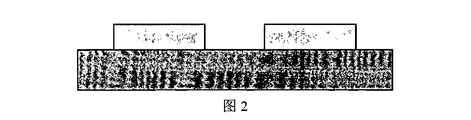
- the bottom electrode material is grown on the substrate by physical vapor deposition (PVD) method, and standard photolithography is used. Technology to pattern the bottom electrode;
- PVD physical vapor deposition
- the top electrode and the bottom electrode are made of W and have a thickness of 200 nm to 500 nm, and the substrate is Silicon substrate.
- the parylene layer as a functional layer has a total thickness of 40 nm to 80 nm and is divided into a plurality of layers. The two layers were exposed to air for 1 day for oxidation of the surface, and the thickness of each layer was controlled to be 10 nm to 20 nm.
- step 2) when the parylene is grown by the Polymer CVD method, the deposition rate is 1 nm/min to 10 nm/min.
- the polymer of parylene is parylene C type, parylene type N or poly pair Xylene type D.
- step 3 is that the user etches into an RIE etch.
- the beneficial effects of the invention under the condition that the basic structure of the device is not changed, the use of both sides is relatively inert
- the electrode and the deposition of a plurality of layers of parylene achieve a multi-value storage function with a self-limiting effect.
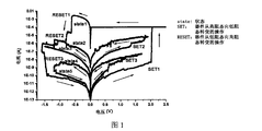
- FIG. 1 is a schematic diagram showing a current-voltage characteristic curve of a resistive process of a multi-valued non-volatile organic resistive memory of the present invention
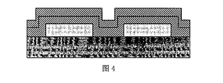
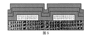
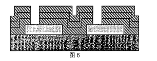
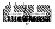
- 2 to 7 are schematic diagrams showing the steps of the steps of the method for preparing a resistive memory in the embodiment.
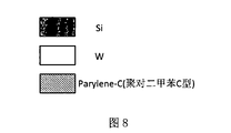
- Figure 8 is a diagrammatic illustration of Figures 2-7.
- the present invention proposes a new resistive memory structure to implement multi-valued storage with self-limiting current characteristics.
- the resistive memory can be fabricated on a silicon substrate, and the device unit is a MIM (Metal-Insulator-Metal) capacitor junction. Structure, using upper and lower layer structure, the intermediate functional layer adopts parylene with excellent resistance change characteristics (parylene-C), the top electrode and the bottom electrode of the MIM structure are preferably W.
- the device is characterized by The parylene layer of the energy layer is deposited multiple times, by the difference in the number of depositions and the thickness of each deposition. To achieve the function of device multi-value storage.
- the device resistance mechanism caused by the active electrode is mainly caused by the diffusion of the electrode.
- the device of the present invention avoids this situation by using W electrodes on both sides, and is formed by The change in resistance determined by the inherent defects in the functional layer of the parylene layer and the interfacial defects of the different layers of parylene.
- the present invention preferably employs an inert electrode W, where inertness is primarily directed to electrode ionization that does not occur. The diffusion into the parylene occurs later.
- Pt electrodes or electrically active TiNs can also be used (but No ionization diffusion will occur) and so on.
- inert electrodes are mainly to avoid the formation of a conductive mode of metal filament channels. Because the formation/breaking of metal filaments is difficult to react completely, it is only necessary to break a layer after the formation of the reset process. Therefore, only a low resistance / high resistance state is shown. Using the defects of parylene itself to conduct electricity can be effectively realized High resistance recovery.
- the current-voltage (I-V) characteristic curve of the resistive memory of the resistive memory of the present invention is shown in FIG.
- a SET RESET for each resistance state of a three-layer parylene (thickness 10/10/20 nm) structure is given.
- the voltage scanning direction of each curve is as shown by the arrow, we can see that there are three different sets of the device SET and RESET processes and three sets of states that can be switched between each other (state1 and state5, state2 and state3, State4 and state5), the SET1 and RESET1 procedures implement the conversion between state1 and state5; SET2 and The RESET2 process implements the conversion between state2 and state3; the SET3 and RESET3 processes implement state4 Conversion between and state5.
- the switching between the three groups of states is completed by the RESET process, we can see
- the curve of RESET1 can be divided into two large mutation phases, corresponding to the device from the state1 state RESET To the state3 and state5 states, so the controller can be adjusted by adjusting the magnitude of the cutoff voltage during RESET1 A transition between different sets of states.
- the state to be utilized is only 2N-1, that is, 5. Since the thickness of the parylene monolayer is difficult to prepare below 10 nm, Under this limitation, after the number of parylene layers increases, the total thickness of the device becomes large, and the state can be effectively distinguished. The number should be less than 2N, but the resistance of the device is reduced after the parylene layer is turned on based on at most half of the thickness. The layer-by-layer conduction of the parylene layer resistance can be distinguished, so that at least N states can be realized. Polylayer The thickness of xylene affects the ratio between a set of low-resistance/high-resistance states corresponding to its turn-on/turn-off. The larger the ratio between the corresponding low resistance/high resistance states. The present invention generally selects a total thickness of parylene of 40 nm. Between 80 nm, the thickness of each layer is controlled between 10 nm and 20 nm.
- Parylene-C (polyparaxylene C type) layer is grown by Polymer CVD technology, as shown in the figure. 3, the layer thickness is 20nm; deposition using poly-p-xylene Polymer CVD equipment, process equipment Standard parameters, deposition rate between 1nm/min and 10nm/min;
- the layer thickness is 10nm; deposition using poly-p-xylene Polymer CVD equipment, process selection equipment standard parameters, deposition rate Degree between 1nm/min and 10nm/min;
- the third layer of Parylene-C layer is grown by Polymer CVD technology, as shown in Figure 5, the layer thickness is 10nm; deposition using poly-p-xylene Polymer CVD equipment, process selection equipment standard parameters, deposition rate Degree between 1nm/min and 10nm/min;
- the thickness is 500 nm, and the standard is used. Quasi-lithography technology to pattern the lower electrode (bottom electrode);
- Parylene-D (polyparaxylene N type) layer is grown by Polymer CVD technology. Degree is 10nm; deposition using poly-p-xylene Polymer CVD equipment, the standard parameters of the process equipment, The product speed is between 1 nm/min and 10 nm/min;
- the thickness of the multilayer parylene in this embodiment is 10/20/10 nm, respectively, and the SET/RESET process occurs.
- the layer is also 10/20/10 nm in order, since the intermediate layer is 20 nm thick, the operating voltage of the intermediate state should be better than that of the embodiment.
- the larger of 1 is also better to distinguish the operating voltage range of different layers of parylene, which can be compared with that in Embodiment 1. Achieve better device performance.
Landscapes
- Engineering & Computer Science (AREA)
- Manufacturing & Machinery (AREA)
- Computer Hardware Design (AREA)
- Physics & Mathematics (AREA)
- Spectroscopy & Molecular Physics (AREA)
- Electromagnetism (AREA)
- Semiconductor Memories (AREA)
Abstract
Description
Claims (10)
- 一种多值非易失性有机阻变存储器,其特征在于,包括顶电极、底电极 以及位于顶电极和底电极之间的中间功能层,所述中间功能层为至少两层聚对二 甲苯。
- 如权利要求1所述多值非易失性有机阻变存储器,其特征在于:所述顶 电极和底电极为惰性电极。
- 如权利要求2所述多值非易失性有机阻变存储器,其特征在于:所述顶 电极和底电极为W电极,厚度为200nm~500nm。
- 如权利要求1所述多值非易失性有机阻变存储器,其特征在于:所述作 为功能层的聚对二甲苯的总厚度为40nm~80nm,每层厚度为10nm~20nm。
- 如权利要求1所述多值非易失性有机阻变存储器,其特征在于:所述聚 对二甲苯的聚合物为聚对二甲苯C型、聚对二甲苯N型或聚对二甲苯D型。
- 一种制备权利要求1所述多值非易失性有机阻变存储器的方法,其步骤 包括:1)采用物理气相淀积方法在衬底上生长底电极材料,并采用标准光刻技术 使底电极图形化;2)采用聚合物化学气相淀积方法在底电极上依次生长多层聚对二甲苯材料;3)通过光刻和刻蚀定义底层电极的引出通孔;4)采用物理气相淀积方法在聚对二甲苯材料上生长顶电极材料,通过光刻、 剥离定义顶层电极,并将底电极引出。
- 如权利要求6所述的方法,其特征在于:所述顶电极和底电极为惰性电 极,所述聚对二甲苯的聚合物为聚对二甲苯C型、聚对二甲苯N型或聚对二甲 苯D型。
- 如权利要求7所述的方法,其特征在于:所述顶电极和底电极为W电极, 厚度为200nm~500nm。
- 如权利要求6所述的方法,其特征在于:所述作为功能层的聚对二甲苯 的总厚度为40nm~80nm,每层厚度为10nm~20nm,两层淀积之间在空气中暴露 一定时间用于表面的氧化。
- 如权利要求6所述的方法,其特征在于:步骤2)采用聚合物化学气相 淀积方法生长聚对二甲苯时,淀积速度为1nm/min~10nm/min。
Priority Applications (1)
| Application Number | Priority Date | Filing Date | Title |
|---|---|---|---|
| US15/024,996 US20160240778A1 (en) | 2014-02-11 | 2014-03-31 | Multi-Value Nonvolatile Organic Resistive Random Access Memory and Method for Preparing the Same |
Applications Claiming Priority (2)
| Application Number | Priority Date | Filing Date | Title |
|---|---|---|---|
| CN201410047253.4A CN103887431B (zh) | 2014-02-11 | 2014-02-11 | 一种多值非易失性有机阻变存储器及制备方法 |
| CN201410047253.4 | 2014-02-11 |
Publications (1)
| Publication Number | Publication Date |
|---|---|
| WO2015120657A1 true WO2015120657A1 (zh) | 2015-08-20 |
Family
ID=50956245
Family Applications (1)
| Application Number | Title | Priority Date | Filing Date |
|---|---|---|---|
| PCT/CN2014/074359 Ceased WO2015120657A1 (zh) | 2014-02-11 | 2014-03-31 | 一种多值非易失性有机阻变存储器及制备方法 |
Country Status (3)
| Country | Link |
|---|---|
| US (1) | US20160240778A1 (zh) |
| CN (1) | CN103887431B (zh) |
| WO (1) | WO2015120657A1 (zh) |
Families Citing this family (1)
| Publication number | Priority date | Publication date | Assignee | Title |
|---|---|---|---|---|
| TWI621017B (zh) * | 2017-03-06 | 2018-04-11 | 慧榮科技股份有限公司 | 資料儲存裝置以及其操作方法 |
Citations (5)
| Publication number | Priority date | Publication date | Assignee | Title |
|---|---|---|---|---|
| WO1999057330A1 (en) * | 1998-05-01 | 1999-11-11 | Desu Seshu B | Oxide/organic polymer multilayer thin films deposited by chemical vapor deposition |
| CN101630719A (zh) * | 2009-07-24 | 2010-01-20 | 北京大学 | 一种阻变存储器及其制备方法 |
| CN102610755A (zh) * | 2012-03-26 | 2012-07-25 | 北京大学 | 一种超低功耗有机阻变存储器件及其制备方法 |
| CN103258957A (zh) * | 2013-05-13 | 2013-08-21 | 北京大学 | 一种有机阻变存储器及制备方法 |
| CN103258958A (zh) * | 2013-05-13 | 2013-08-21 | 北京大学 | 有机阻变存储器及其制备方法 |
Family Cites Families (3)
| Publication number | Priority date | Publication date | Assignee | Title |
|---|---|---|---|---|
| CN101630718B (zh) * | 2009-07-24 | 2012-01-18 | 北京大学 | 一种阻变存储器及其制备方法 |
| US9847478B2 (en) * | 2012-03-09 | 2017-12-19 | Taiwan Semiconductor Manufacturing Company, Ltd. | Methods and apparatus for resistive random access memory (RRAM) |
| CN103078053A (zh) * | 2012-12-21 | 2013-05-01 | 北京大学 | 一种多值阻变存储器及其制备方法 |
-
2014
- 2014-02-11 CN CN201410047253.4A patent/CN103887431B/zh active Active
- 2014-03-31 US US15/024,996 patent/US20160240778A1/en not_active Abandoned
- 2014-03-31 WO PCT/CN2014/074359 patent/WO2015120657A1/zh not_active Ceased
Patent Citations (5)
| Publication number | Priority date | Publication date | Assignee | Title |
|---|---|---|---|---|
| WO1999057330A1 (en) * | 1998-05-01 | 1999-11-11 | Desu Seshu B | Oxide/organic polymer multilayer thin films deposited by chemical vapor deposition |
| CN101630719A (zh) * | 2009-07-24 | 2010-01-20 | 北京大学 | 一种阻变存储器及其制备方法 |
| CN102610755A (zh) * | 2012-03-26 | 2012-07-25 | 北京大学 | 一种超低功耗有机阻变存储器件及其制备方法 |
| CN103258957A (zh) * | 2013-05-13 | 2013-08-21 | 北京大学 | 一种有机阻变存储器及制备方法 |
| CN103258958A (zh) * | 2013-05-13 | 2013-08-21 | 北京大学 | 有机阻变存储器及其制备方法 |
Also Published As
| Publication number | Publication date |
|---|---|
| US20160240778A1 (en) | 2016-08-18 |
| CN103887431B (zh) | 2017-01-04 |
| CN103887431A (zh) | 2014-06-25 |
Similar Documents
| Publication | Publication Date | Title |
|---|---|---|
| US11659781B2 (en) | Selector device and method of making the same | |
| CN101919056B (zh) | 采用形成在下部导体上方的选择性制造的碳纳米管可逆电阻转换元件的存储器单元及其形成方法 | |
| US8699259B2 (en) | Non-volatile storage system using opposite polarity programming signals for MIM memory cell | |
| JP5469159B2 (ja) | カーボンナノチューブ可逆抵抗スイッチング素子を含むメモリセルおよびその形成方法 | |
| CN103606625B (zh) | 高一致性低功耗阻变存储器及制备方法 | |
| US20080237599A1 (en) | Memory cell comprising a carbon nanotube fabric element and a steering element | |
| US20100117041A1 (en) | Resistive memory device and method of fabricating the same | |
| JP2013062401A (ja) | 抵抗変化型不揮発記憶装置、半導体装置及び抵抗変化型不揮発記憶装置の動作方法 | |
| US20110095434A1 (en) | Apparatus and methods of forming memory lines and structures using double sidewall patterning for four times half pitch relief patterning | |
| JP2011508458A (ja) | 選択的に製造されたカーボンナノチューブ可逆抵抗切替素子を使用するメモリセルおよびそれを形成する方法 | |
| CN101919048A (zh) | 具有平坦化碳纳米管层的存储器单元及其制造方法 | |
| WO2008118486A1 (en) | Memory cell comprising a carbon nanotube fabric element and a steering element and methods of forming the same | |
| WO2016068745A1 (en) | Memory apparatus and method of production thereof | |
| JP2014017379A (ja) | 不揮発性記憶装置 | |
| CN101630718B (zh) | 一种阻变存储器及其制备方法 | |
| US20090302301A1 (en) | Resistance ram device having a carbon nano-tube and method for manufacturing the same | |
| CN104465989A (zh) | 三端原子开关器件及其制备方法 | |
| CN103258958B (zh) | 有机阻变存储器及其制备方法 | |
| CN110752293A (zh) | 一种双向阈值开关选择器件及其制备方法 | |
| CN103078053A (zh) | 一种多值阻变存储器及其制备方法 | |
| KR20130007483A (ko) | 그래핀을 이용한 메모리 소자 및 이의 제조방법 | |
| WO2015120657A1 (zh) | 一种多值非易失性有机阻变存储器及制备方法 | |
| CN103258957B (zh) | 一种有机阻变存储器及制备方法 | |
| Cha et al. | Selector devices for 3-D cross-point ReRAM | |
| CN108962932A (zh) | 单一堆叠结构的1d1r存储器及其制备方法 |
Legal Events
| Date | Code | Title | Description |
|---|---|---|---|
| 121 | Ep: the epo has been informed by wipo that ep was designated in this application |
Ref document number: 14882273 Country of ref document: EP Kind code of ref document: A1 |
|
| WWE | Wipo information: entry into national phase |
Ref document number: 15024996 Country of ref document: US |
|
| NENP | Non-entry into the national phase |
Ref country code: DE |
|
| 32PN | Ep: public notification in the ep bulletin as address of the adressee cannot be established |
Free format text: NOTING OF LOSS OF RIGHTS PURSUANT TO RULE 112(1) EPC (EPO FORM 1205A DATED 24/11/2016) |
|
| 122 | Ep: pct application non-entry in european phase |
Ref document number: 14882273 Country of ref document: EP Kind code of ref document: A1 |