WO2015115136A1 - 成膜マスクの製造方法及び成膜マスク - Google Patents
成膜マスクの製造方法及び成膜マスク Download PDFInfo
- Publication number
- WO2015115136A1 WO2015115136A1 PCT/JP2015/050227 JP2015050227W WO2015115136A1 WO 2015115136 A1 WO2015115136 A1 WO 2015115136A1 JP 2015050227 W JP2015050227 W JP 2015050227W WO 2015115136 A1 WO2015115136 A1 WO 2015115136A1
- Authority
- WO
- WIPO (PCT)
- Prior art keywords
- film
- metal material
- magnetic metal
- material layer
- gap
- Prior art date
- Legal status (The legal status is an assumption and is not a legal conclusion. Google has not performed a legal analysis and makes no representation as to the accuracy of the status listed.)
- Ceased
Links
Images



Classifications
-
- B—PERFORMING OPERATIONS; TRANSPORTING
- B23—MACHINE TOOLS; METAL-WORKING NOT OTHERWISE PROVIDED FOR
- B23K—SOLDERING OR UNSOLDERING; WELDING; CLADDING OR PLATING BY SOLDERING OR WELDING; CUTTING BY APPLYING HEAT LOCALLY, e.g. FLAME CUTTING; WORKING BY LASER BEAM
- B23K26/00—Working by laser beam, e.g. welding, cutting or boring
- B23K26/36—Removing material
- B23K26/38—Removing material by boring or cutting
- B23K26/382—Removing material by boring or cutting by boring
-
- C—CHEMISTRY; METALLURGY
- C23—COATING METALLIC MATERIAL; COATING MATERIAL WITH METALLIC MATERIAL; CHEMICAL SURFACE TREATMENT; DIFFUSION TREATMENT OF METALLIC MATERIAL; COATING BY VACUUM EVAPORATION, BY SPUTTERING, BY ION IMPLANTATION OR BY CHEMICAL VAPOUR DEPOSITION, IN GENERAL; INHIBITING CORROSION OF METALLIC MATERIAL OR INCRUSTATION IN GENERAL
- C23C—COATING METALLIC MATERIAL; COATING MATERIAL WITH METALLIC MATERIAL; SURFACE TREATMENT OF METALLIC MATERIAL BY DIFFUSION INTO THE SURFACE, BY CHEMICAL CONVERSION OR SUBSTITUTION; COATING BY VACUUM EVAPORATION, BY SPUTTERING, BY ION IMPLANTATION OR BY CHEMICAL VAPOUR DEPOSITION, IN GENERAL
- C23C14/00—Coating by vacuum evaporation, by sputtering or by ion implantation of the coating forming material
- C23C14/04—Coating on selected surface areas, e.g. using masks
- C23C14/042—Coating on selected surface areas, e.g. using masks using masks
-
- H—ELECTRICITY
- H10—SEMICONDUCTOR DEVICES; ELECTRIC SOLID-STATE DEVICES NOT OTHERWISE PROVIDED FOR
- H10K—ORGANIC ELECTRIC SOLID-STATE DEVICES
- H10K71/00—Manufacture or treatment specially adapted for the organic devices covered by this subclass
- H10K71/10—Deposition of organic active material
- H10K71/16—Deposition of organic active material using physical vapour deposition [PVD], e.g. vacuum deposition or sputtering
- H10K71/166—Deposition of organic active material using physical vapour deposition [PVD], e.g. vacuum deposition or sputtering using selective deposition, e.g. using a mask
Definitions
- the present invention relates to a method of manufacturing a film formation mask having a structure in which a resin film layer having an opening pattern formed thereon and a magnetic metal material layer are laminated, and particularly when forming the opening pattern by laser processing, the edge of the opening pattern.
- the present invention relates to a film forming mask manufacturing method and a film forming mask that can suppress the generation of burrs.
- a conventional method of manufacturing this type of mask is to use a patterned mask to irradiate a resin film with, for example, a KrF excimer laser beam having a short wavelength of about 248 nm, and then ablate the resin film.
- An opening pattern is formed (for example, see Patent Document 1).
- an opening pattern is usually formed by irradiating one surface side of a resin film with a laser beam, so the opening pattern is opposite to the laser beam irradiation side.
- burrs uncut edges
- Such burrs cause shadows in the film formation and cause a disorder in the shape of the edge of the thin film pattern to be formed, or create a gap between the film formation mask and the film formation substrate. There is a possibility that the material may easily go under the mask and cause the problem that the edge of the thin film pattern is blurred.
- the present invention addresses such problems, and a method of manufacturing a film formation mask and film formation that can suppress the occurrence of burrs at the edge of the opening pattern when forming the opening pattern by laser processing.
- the object is to provide a mask.
- a method of manufacturing a film formation mask according to the present invention includes a resin film layer provided with an opening pattern having a predetermined shape, and a gap having a size capable of containing the opening pattern.
- the film-forming mask according to the present invention includes a resin film layer provided with an opening pattern having a predetermined shape, and a magnetic metal material layer provided with a gap having a size capable of containing the opening pattern.
- the opening pattern is formed by irradiating a part of the film layer corresponding to the gap with laser light from both sides to penetrate the film layer.
- the opening pattern is formed by irradiating the laser beam from both sides of the film layer, so that the side opposite to the magnetic metal material layer of the film layer (the side of the adhesion surface with the deposition substrate) ) Can be prevented from occurring at the edge of the opening pattern. Therefore, the burr in the opening pattern can be prevented from being a shadow of film formation, and a gap can be prevented from being generated between the film layer and the film formation substrate due to the presence of the burr. Thereby, the formation precision of a thin film pattern including a shape and position accuracy can be improved.
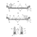
- FIG. 1A and 1B are views showing an embodiment of a film-forming mask according to the present invention, in which FIG. 1A is a plan view, FIG. 1B is a cross-sectional view taken along the line OO in FIG. P line sectional arrow view, (d) is a partially enlarged sectional view of (c). It is a top view which shows the modification of the magnetic metal material layer of the film-forming mask by this invention. It is a figure explaining the formation example of an opening pattern with the manufacturing method of the film-forming mask by this invention, It is sectional drawing which shows the formation process of the 1st recessed part, (a) shows the laser processing start, (b) The end of laser processing is shown, (c) is an enlarged cross-sectional view of the first recess.
- FIG. 1A and 1B are diagrams showing an embodiment of a film-forming mask according to the present invention, where FIG. 1A is a plan view, FIG. 1B is a cross-sectional view taken along the line OO in FIG. 1A, and FIG. FIG. 4D is a partially enlarged cross-sectional view of FIG.
- This film formation mask is for forming a plurality of thin film patterns having a predetermined shape on a film formation substrate, and includes a film layer 1, a magnetic metal material layer 2, and a frame 3. ing.
- the film layer 1 serves as a main mask for forming a thin film pattern on the deposition substrate, and transmits visible light such as polyimide or polyethylene terephthalate (PET) having a thickness of about 5 ⁇ m to 30 ⁇ m.
- an opening pattern 4 having a predetermined shape is provided on a resin film.
- a polyimide whose linear expansion coefficient is about 3 ⁇ 10 ⁇ 6 to 5 ⁇ 10 ⁇ 6 / ° C., which approximates the linear expansion coefficient of glass as a deposition target substrate (hereinafter simply referred to as “substrate”) is desirable.
- the opening pattern 4 has the same shape as the thin film pattern, and is arranged in a matrix form corresponding to the thin film pattern, as shown in FIG.
- the first concave portion 5 having a depth of, for example, about 4 ⁇ m to 5 ⁇ m formed on one surface 1a of the film layer 1 and the depth reaching the first concave portion 5 on the other surface 1b of the film layer 1 are formed.
- a second recess 6 In this case, the opening area of the second recess 6 is preferably larger than the opening area of the first recess 5.
- the 1st recessed part 5 may be the through-hole 13 (refer FIG. 5) which penetrates the film layer 1 so that it may mention later.
- a magnetic metal material layer 2 is laminated on the other surface 1 b side of the film layer 1.
- the magnetic metal material layer 2 is made of a magnetic metal material such as nickel, nickel alloy, invar or invar alloy, for example, having a thickness 7 of about 10 ⁇ m to 50 ⁇ m, with a gap 7 large enough to contain the opening pattern 4.
- the film layer 1 is attracted by a magnet disposed on the back surface of the substrate during film formation, and functions to bring the film layer 1 into close contact with the film formation surface of the substrate.
- the gap 7 is a slit provided through the magnetic metal material layer 2 as shown in FIGS. 1 (a) to 1 (c).
- a plurality of elongated island patterns 8 constituting a part of the magnetic metal material layer 2 may be a portion between the adjacent island patterns 8.
- the magnetic metal material layer 2 includes the island pattern 8 as shown in FIG. 2
- the magnetic metal material layer 2 is generated in the film layer 1 due to a difference in linear expansion coefficient between the magnetic metal material layer 2 and the film layer 1.
- the internal stress to be reduced is reduced, and the positional deviation of the opening pattern 4 formed by laser processing after lamination can be suppressed. Therefore, there is an effect that the selection range of the magnetic metal material is expanded.
- the island pattern 8 may be divided into a plurality of unit island patterns having a short length in the major axis direction. Thereby, the internal stress which generate
- reference numeral 9 denotes a frame-shaped pattern that has an opening having a size that includes the plurality of island patterns 8 and is part of the magnetic metal material layer 2 that is laminated on the peripheral edge of the film layer 1. is there.
- a frame 3 is provided on the surface 2 a of the magnetic metal material layer 2 opposite to the film layer 1.
- the frame 3 fixes and supports the periphery of the magnetic metal material layer 2 and is formed of a magnetic metal material made of, for example, invar or iron-nickel alloy. It forms a frame shape having an opening 10 sized to enclose the gap 7.
- the frame 3 is not limited to one made of a magnetic metal material, and may be made of a nonmagnetic metal material or a hard resin. In the present embodiment, the frame 3 is made of a magnetic metal material.
- a metal sheet of a magnetic metal material having a thickness of about 10 ⁇ m to 50 ⁇ m made of, for example, nickel, nickel alloy, invar or invar alloy is cut out according to the surface area of the substrate to be deposited, A polyimide resin solution is applied and dried at a temperature of about 200 ° C. to 300 ° C. to form a film layer 1 that transmits visible light having a thickness of about 5 ⁇ m to 30 ⁇ m.
- the resist film is dried to form a resist film.
- the resist film is exposed using a photomask, and then developed to develop a plurality of rows.
- a resist mask having a plurality of elongated openings is formed corresponding to the slit formation position.
- the metal sheet corresponding to the opening of the resist mask is removed, and a slit penetrating the metal sheet is provided to form the magnetic metal material layer 2
- the resist mask is removed by dissolving it in an organic solvent, for example.
- a mask member 11 in which the film layer 1 and the magnetic metal material layer 2 are laminated is formed.
- the etching liquid for etching a metal sheet is suitably selected according to the material of the metal sheet to be used, and a well-known technique can be applied.
- the mask side alignment for aligning with a substrate side alignment mark previously provided on the substrate at a predetermined position outside the formation region of the plurality of slits.
- the mark 12 may be formed simultaneously. In this case, when the resist mask is formed, an alignment mark opening may be provided at a position corresponding to the mask side alignment mark 12.
- the mask member 11 may be formed by other methods without depending on the above method.
- a seed layer is formed on one surface of the film by, for example, electroless plating, a photoresist is applied thereon, exposed and developed, and a plurality of rows of island-shaped resins corresponding to the positions where the plurality of rows of slits are formed.
- a magnetic metal material such as nickel, nickel alloy, invar or invar alloy is plated on the outer region of the island-shaped resin pattern.
- the mask member 11 may be formed by etching and removing the seed layer at the formation position of the island-shaped resin pattern.
- the mask member 11 including the magnetic metal material layer 2 in which a plurality of slits as shown in FIG.
- the mask member 11 including the frame-shaped pattern 9 and the magnetic metal material layer 2 provided with a plurality of island patterns 8 inside the frame-shaped pattern 9 is formed as follows. It can be carried out. For example, a seed layer is formed on one surface of the film by, for example, electroless plating, a photoresist is applied thereon, and this is exposed and developed, so that the frame-shaped pattern 9 and the plurality of island patterns 8 are formed. After forming the resin pattern covering the outer seed layer, a magnetic metal material such as nickel, nickel alloy, invar or invar alloy is formed by plating at the position where the frame pattern 9 and the plurality of island patterns 8 are to be formed. Then, after removing the resin pattern, the seed layer at the position where the resin pattern is formed is removed by etching.
- a seed layer is formed on one surface of the film by, for example, electroless plating, a photoresist is applied thereon, and this is exposed and developed, so that the frame-shaped pattern 9 and the plurality of island patterns 8 are formed.
- the resin layer is applied to one surface of the metal sheet to form the film layer 1
- the resist is applied to the other surface of the metal sheet and dried, and then the photomask is applied.
- the resist is exposed to light and developed to form a resist mask having an opening outside the position where the frame-like pattern 9 and the plurality of island patterns 8 are to be formed, and the magnetic metal sheet is formed using the resist mask.
- the mask member 11 including the magnetic metal material layer 2 having the frame pattern 9 and the plurality of island patterns 8 may be formed by etching.
- the mask member 11 is arranged with the frame 3 made of a magnetic metal material facing the magnetic metal material layer 2 of the mask member 11 and the mask member 11 stretched on the frame 3. 11 is irradiated with laser light to spot weld the magnetic metal material layer 2 to the end face of the frame 3.
- the process proceeds to an opening pattern forming process which is a feature of the present invention.
- the opening pattern forming process will be described with reference to FIGS.
- a third harmonic of an excimer laser of KrF 248 nm or a YAG laser for example, a third harmonic of an excimer laser of KrF 248 nm or a YAG laser.
- a wave or a fourth harmonic a laser beam L having a wavelength of 400 nm or less is irradiated, the film layer 1 is ablated, and a first recess 5 having a constant depth is provided as shown in FIG. .
- the film layer 1 is moved by moving a laser beam by a predetermined distance in a two-dimensional direction in a plane parallel to the surface of the mask member 11 with reference to a mask alignment mark 12 formed in advance.
- a portion corresponding to the gap 7 of the magnetic metal material layer 2 is irradiated with the laser beam L on the one surface 1a to form the first recess 5.
- the mask member 11 is positioned and placed on a reference substrate provided with a reference pattern that is an irradiation target of the laser light L at a position corresponding to the opening pattern 4 to be formed, and transmitted through the film layer 1.
- the irradiation target of the laser beam L is set to the position coordinates of the reference pattern, and the laser beam is applied to one surface 1a of the film layer 1 L may be irradiated to form the first recess 5.
- FIG. 3 shows a case where a plurality of first recesses 5 shown in FIG.
- the laser beam L is ablated on one surface 1a of the film layer 1 while stepping the laser beam L on the one surface 1a of the film layer 1 by a predetermined distance in the two-dimensional direction indicated by the arrow.
- a plurality of first recesses 5 are formed in one surface 1a of the film layer 1 in a vertical and horizontal matrix form.
- the mask member 11 is turned upside down, and the surface from the magnetic metal material layer 2 side to the magnetic metal material layer 2 side of the film layer 1 (hereinafter referred to as “other surface 1b”) as shown in FIG. ) Is irradiated with the laser beam L, and the second recess 6 reaching the first recess 5 is formed in the portion of the film layer 1 corresponding to the gap 7 of the magnetic metal material layer 2.
- the first recess 5 and the second recess 6 are connected to form an opening pattern 4 penetrating the film layer 1.
- the opening area of the second recess 6 is larger than the opening area of the first recess 5.
- a projection type laser processing apparatus using a shadow mask provided with a plurality of similar openings in the second recess 6 is used, and the plurality of openings are formed in the other surface 1b of the film layer 1.
- the plurality of second recesses 6 may be formed collectively by projecting a reduced portion.
- the second recess 6 may be formed by using the laser light L corresponding to the area of the region including the plurality of first recesses 5 with the irradiation area.
- the magnetic metal material layer 2 functions as a mask, and the portion of the film layer 1 corresponding to the gap 7 of the magnetic metal material layer 2 is ablated to form the second recess 6.
- the laser beam L is moved stepwise on the other surface 1b of the film layer 1 by a predetermined distance in the two-dimensional direction indicated by the arrow, and the other surface 1b of the film layer 1 is moved.
- Ablation is performed to form a plurality of second recesses 6 on the other surface 1b of the film layer 1 as shown in FIG.
- the film-forming mask shown in FIG. 1 or FIG. 2 is formed.
- the laser beam L is irradiated from both sides of the film layer 1 to form the opening pattern 4, so one side of the film layer 1 (contact surface with the substrate) 1 a side
- the occurrence of burrs at the edge of the opening pattern 4 can be suppressed. Therefore, it is possible to prevent the burr of the opening pattern 4 from being a shadow of film formation, and to prevent a gap from being generated between the film layer 1 and the substrate due to the presence of the burr. Thereby, the formation precision of a thin film pattern including a shape and position accuracy can be improved.
- the second concave portion 6 having a larger area than the opening area of the first concave portion 5 is formed after the first concave portion 5 is formed, the generation of the burr can be further suppressed. Moreover, since the opening area of the 2nd recessed part 6 is larger than that of the 1st recessed part 5, the process positioning accuracy of the 2nd recessed part 6 can be made unnecessary.
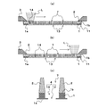
- FIG. 5 is a view for explaining a modified example of the formation of the opening pattern in the method for manufacturing a film forming mask according to the present invention.
- FIG. 5 is a cross-sectional view showing a through hole forming process, (a) shows the start of laser processing, b) shows the end of laser processing, and (c) is an enlarged sectional view of the through hole.
- FIG. 6 is a view for explaining a modified example of the formation of the opening pattern in the method for manufacturing a film formation mask according to the present invention.
- FIG. 6 is a cross-sectional view showing the step of forming the recesses.
- FIG. 5 (a) Indicates the end of laser processing, and (c) is an enlarged cross-sectional view of the recess.
- FIG. 5 (a) one surface 1a of the film layer 1 is irradiated with a laser beam L to ablate the film layer 1, and a through-hole penetrating the film layer 1 as shown in FIG. 5 (c). 13 is provided.
- the laser beam is moved by a predetermined distance in a two-dimensional direction in a plane parallel to the surface of the mask member 11 with reference to the mask-side alignment mark 12 formed in advance. And the laser beam L is irradiated to the part corresponding to the clearance gap 7 of the magnetic metal material layer 2 in the one surface 1a of the film layer 1, and the through-hole 13 of the same shape as a thin film pattern is formed.
- the mask member 11 is positioned and placed on a reference substrate provided with a reference pattern that is an irradiation target of the laser light L at a position corresponding to the opening pattern 4 to be formed, and transmitted through the film layer 1.
- the irradiation target of the laser beam L is set to the position coordinates of the reference pattern, and the laser beam is applied to one surface 1a of the film layer 1 L may be irradiated to form the through hole 13.
- the laser beam L is ablated on one surface 1a of the film layer 1 while stepping the laser beam L on the one surface 1a of the film layer 1 by a predetermined distance in the two-dimensional direction indicated by the arrow.
- a plurality of through holes 13 are formed in one surface 1a of the film layer 1 in a vertical and horizontal matrix form.
- the mask member 11 is turned upside down, and the other surface 1b of the film layer 1 is irradiated with the laser light L from the magnetic metal material layer 2 side as shown in FIG.
- a recess 14 having an opening larger than the opening area of the through hole 13 is formed in the portion of the film layer 1 corresponding to the gap 7 of the film layer 1 while leaving a thin layer of about 1 ⁇ m to 4 ⁇ m on the one surface 1a side of the film layer 1.
- the opening pattern 4 comprised by the through-hole 13 and the recessed part 14 is formed in the film layer 1.
- the laser beam L is moved stepwise on the other surface 1b of the film layer 1 by a predetermined distance in the two-dimensional direction indicated by the arrow, and the other surface 1b of the film layer 1 is moved. Ablation is performed to form a plurality of recesses 14 on the other surface 1b of the film layer 1 as shown in FIG. Thereby, the film-forming mask shown in FIG. 1 or FIG. 2 is formed.
- the opening pattern 4 is formed by irradiating the laser beam L from both sides of the film layer 1, the edge of the opening pattern 4 on the one side (contact surface with the substrate) 1a side of the film layer 1 Generation of burrs can be suppressed.
- the film formation mask according to the present invention can improve the adhesion to the substrate, and is suitable for vapor deposition formation of an organic EL layer including a light emitting layer of an organic EL display substrate, for example.
- the present invention is not limited to this, and the frame 3 may be omitted.
Landscapes
- Engineering & Computer Science (AREA)
- Chemical & Material Sciences (AREA)
- Mechanical Engineering (AREA)
- Chemical Kinetics & Catalysis (AREA)
- Plasma & Fusion (AREA)
- Optics & Photonics (AREA)
- Physics & Mathematics (AREA)
- Materials Engineering (AREA)
- Metallurgy (AREA)
- Organic Chemistry (AREA)
- Manufacturing & Machinery (AREA)
- Physical Vapour Deposition (AREA)
- Laser Beam Processing (AREA)
- Drying Of Semiconductors (AREA)
- Preparing Plates And Mask In Photomechanical Process (AREA)
Abstract
本発明は、予め定められた所定形状の開口パターン4を設けた樹脂製のフィルム層1と、前記開口パターン4が内在し得る大きさの隙間7を設けた磁性金属材料層2とを積層した構造の成膜マスクの製造方法であって、前記開口パターン4は、前記隙間7に対応したフィルム層1の部分に両面側からレーザ光を照射し、前記フィルム層2を貫通させて形成されるものである。
Description
本発明は、開口パターンを形成した樹脂製のフィルム層と磁性金属材料層とを積層した構造の成膜マスクの製造方法に関し、特にレーザ加工により開口パターンを形成する際に、開口パターンの縁部にバリが発生するのを抑制し得る成膜マスクの製造方法及び成膜マスクに係るものである。
従来のこの種のマスクの製造方法は、パターン化されたマスクを使用して樹脂製フィルムに、例えばKrFエキシマレーザの約248nmの短波長光のビームを照射し、上記樹脂製フィルムをアブレーションして開口パターンを形成するものとなっていた(例えば、特許文献1参照)。
しかし、このような従来のマスクの製造方法においては、通常、樹脂製フィルムの一方の面側にレーザ光を照射して開口パターンを形成するため、開口パターンの、レーザ光の照射側とは反対側の開口縁部に切り残り(以下「バリ」という)が発生するという問題がある。
このようなバリは、成膜の影を形成して成膜される薄膜パターンの縁部の形状乱れを生じさせたり、成膜マスクと被成膜基板との間に隙間を生じさせて成膜材料がマスクの下側に回り込み易くし、薄膜パターンの縁部をぼやけさせてしまったりという問題の発生原因となるおそれがある。
そこで、本発明は、このような問題点に対処し、レーザ加工により開口パターンを形成する際に、開口パターンの縁部にバリが発生するのを抑制し得る成膜マスクの製造方法及び成膜マスクを提供することを目的とする。
上記目的を達成するために、本発明による成膜マスクの製造方法は、予め定められた所定形状の開口パターンを設けた樹脂製のフィルム層と、前記開口パターンが内在し得る大きさの隙間を設けた磁性金属材料層とを積層した構造の成膜マスクの製造方法であって、前記開口パターンは、前記隙間に対応したフィルム層の部分に両面側からレーザ光を照射し、前記フィルム層を貫通させて形成されるものである。
また、本発明による成膜マスクは、予め定められた所定形状の開口パターンを設けた樹脂製のフィルム層と、前記開口パターンが内在し得る大きさの隙間を設けた磁性金属材料層とを積層した構造の成膜マスクであって、前記開口パターンは、前記隙間に対応したフィルム層の部分に両面側からレーザ光を照射し、前記フィルム層を貫通させたものである。
本発明によれば、フィルム層の両面側からレーザ光を照射し、開口パターンを形成するようにしているので、フィルム層の磁性金属材料層とは反対側(被成膜基板との密着面側)の開口パターンの縁部にバリが発生するのを抑制することができる。したがって、開口パターンの上記バリが成膜の影となるのを防止することができると共に、バリの存在によりフィルム層と被成膜基板との間に隙間が生じるのを防止することができる。これにより、形状及び位置精度を含む薄膜パターンの形成精度を向上することができる。
以下、本発明の実施形態を添付図面に基づいて詳細に説明する。図1は本発明による成膜マスクの一実施形態を示す図であり、(a)は平面図、(b)は(a)のO-O線断面矢視図、(c)は(a)のP-P線断面矢視図、(d)は(c)の一部拡大断面図である。この成膜マスクは、被成膜基板上に予め定められた形状の複数の薄膜パターンを形成するためのもので、フィルム層1と、磁性金属材料層2と、フレーム3とを備えて構成されている。
上記フィルム層1は、被成膜基板上に薄膜パターンを成膜するためのメインマスクとなるもので、例えば厚みが5μm~30μm程度の、例えばポリイミドやポリエチレンテレフタレート(PET)等の可視光を透過する樹脂製のフィルムに、図1(a)に示すように、予め定められた形状の開口パターン4を備えたものである。好ましくは、線膨張係数が被成膜基板(以下、単に「基板」という)としてのガラスの線膨張係数に近似した3×10⁻⁶~5×10⁻⁶/℃程度のポリイミドが望ましい。
詳細には、上記開口パターン4は、図1(a)に示すように、上記薄膜パターンと同形状を有し、薄膜パターンに対応して縦横マトリクス状に配置して、同図(d)に示すようにフィルム層1の一面1aに形成された、例えば4μm~5μm程度の深さの第1の凹部5と、フィルム層1の他面1bに第1の凹部5に達する深さで形成された第2の凹部6とから成る。この場合、好ましくは、第2の凹部6の開口面積は、第1の凹部5の開口面積よりも広いことが望ましい。なお、第1の凹部5は、後述するように、フィルム層1を貫通する貫通孔13(図5参照)であってもよい。
上記フィルム層1の他面1b側には、磁性金属材料層2が積層して設けられている。この磁性金属材料層2は、開口パターン4が内在し得る大きさの隙間7を設けた、例えば厚みが10μm~50μm程度の、例えばニッケル、ニッケル合金、インバー又はインバー合金等の磁性金属材料から成るもので、成膜時に基板の裏面に配設された磁石により吸引されて上記フィルム層1を基板の成膜面に密着させるための機能を果たすものである。
この場合、上記隙間7は、図1(a)~(c)に示すように、磁性金属材料層2を貫通して設けられたスリットである。又は、図2に示すように、磁性金属材料層2の一部を成す細長状の複数の島パターン8にて、隣接する上記島パターン8の間の部分であってもよい。磁性金属材料層2が図2に示すような島パターン8を含む構成の場合には、磁性金属材料層2とフィルム層1との間の線膨張係数の違いに起因してフィルム層1に発生する内部応力が小さくなり、積層後にレーザ加工して形成される開口パターン4の位置ずれを抑制することができる。したがって、磁性金属材料の選択範囲が広がる効果がある。なお、上記島パターン8は、その長軸方向に長さの短い複数の単位島パターンに分割されてもよい。これにより、フィルム層1に発生する内部応力をより小さくすることができる。図2において、符号9は、上記複数の島パターン8を内包する大きさの開口を有し、フィルム層1の周縁部に積層された、磁性金属材料層2の一部を成す枠状パターンである。
上記磁性金属材料層2の上記フィルム層1とは反対側の面2aには、フレーム3が設けられている。このフレーム3は、上記磁性金属材料層2の周縁部を固定して支持するもので、例えばインバー又は鉄-ニッケル合金等から成る磁性金属材料で形成されており、上記磁性金属材料層2の複数の隙間7を内包する大きさの開口10を有する枠状を成している。なお、フレーム3は、磁性金属材料から成るものに限られず、非磁性金属材料又は硬質樹脂から成るものであってもよい。本実施形態においては、フレーム3は磁性金属材料で形成されている。
次に、このように構成された成膜マスクの製造方法について説明する。
先ず、例えばニッケル、ニッケル合金、インバー又はインバー合金等からなる厚みが10μm~50μm程度の磁性金属材料の金属シートを、成膜対象である基板の表面積に合わせて切り出し、該金属シートの一面に例えばポリイミドの樹脂液を塗布し、これを200℃~300℃程度の温度で乾燥させて厚みが5μm~30μm程度の可視光を透過するフィルム層1を形成する。
先ず、例えばニッケル、ニッケル合金、インバー又はインバー合金等からなる厚みが10μm~50μm程度の磁性金属材料の金属シートを、成膜対象である基板の表面積に合わせて切り出し、該金属シートの一面に例えばポリイミドの樹脂液を塗布し、これを200℃~300℃程度の温度で乾燥させて厚みが5μm~30μm程度の可視光を透過するフィルム層1を形成する。
次いで、金属シートの他面にレジストを例えばスプレー塗布した後、これを乾燥させてレジストフィルムを形成し、次に、フォトマスクを使用してレジストフィルムを露光した後、現像して、複数列のスリットの形成位置に対応させて細長状の複数の開口を有するレジストマスクを形成する。
続いて、上記レジストマスクを使用して金属シートをウェットエッチングし、レジストマスクの開口に対応した部分の金属シートを除去して金属シートを貫通するスリットを設けて磁性金属材料層2を形成した後、レジストマスクを例えば有機溶剤に溶解させて除去する。これにより、フィルム層1と磁性金属材料層2とを積層させたマスク用部材11(図3参照)が形成される。なお、金属シートをエッチングするためのエッチング液は、使用する金属シートの材料に応じて適宜選択され、公知の技術を適用することができる。
また、金属シートをエッチングしてスリットを形成する際に、複数のスリットの形成領域外の予め定められた位置に基板に予め設けられた基板側アライメントマークに対して位置合わせするためのマスク側アライメントマーク12(図1,2参照)を同時に形成してもよい。この場合、レジストマスクを形成する際に、マスク側アライメントマーク12に対応した位置にアライメントマーク用の開口を設けるとよい。
マスク用部材11は上記方法によらず、他の方法で形成してもよい。例えば、フィルムの一面にシード層を例えば無電解めっきにより形成し、その上にフォトレジストを塗布してこれを露光及び現像し、複数列のスリットの形成位置に対応させて複数列の島状樹脂パターンを形成した後、該島状樹脂パターンの外側領域にニッケル、ニッケル合金、インバー又はインバー合金等の磁性金属材料をめっき形成する。そして、島状樹脂パターンを除去した後、該島状樹脂パターンの形成位置のシード層をエッチングして除去することによりマスク用部材11を形成してもよい。
これにより、図1(a)に示すような複数のスリットをその長軸と交差する方向に並設した磁性金属材料層2を備えるマスク用部材11を形成することができる。
また、図2に示すような、枠状パターン9及び該枠状パターン9の内側に複数の島パターン8を設けた磁性金属材料層2を備えるマスク用部材11の形成は、次のようにして行うことができる。例えば、フィルムの一面にシード層を例えば無電解めっきにより形成し、その上にフォトレジストを塗布してこれを露光及び現像し、枠状パターン9及び複数の島パターン8を形成しようとする位置の外側のシード層を覆う樹脂パターンを形成した後、上記枠状パターン9及び複数の島パターン8を形成しようとする位置にニッケル、ニッケル合金、インバー又はインバー合金等の磁性金属材料をめっき形成する。そして、樹脂パターンを除去した後、該樹脂パターンの形成位置のシード層をエッチングして除去する。
又は、前述と同様にして、金属シートの一面に樹脂液を塗布してフィルム層1を形成し、金属シートの他面には、レジストを塗布して、これを乾燥させた後、フォトマスクを使用してレジストを露光及び現像し、上記枠状パターン9及び複数の島パターン8を形成しようとする位置の外側に開口を有するレジストマスクを形成し、該レジストマスクを使用して上記磁性金属シートをエッチングすることにより、枠状パターン9及び複数の島パターン8を有する磁性金属材料層2を備えるマスク用部材11を形成してもよい。
次に、上記マスク用部材11の磁性金属材料層2に対面させて、磁性金属材料から成るフレーム3を配置し、上記マスク用部材11を上記フレーム3上に架張した状態で、マスク用部材11の周縁部にレーザ光を照射して磁性金属材料層2をフレーム3の端面にスポット溶接する。
続いて、本発明の特徴である開口パターン形成工程に移る。以下、開口パターン形成工程について図3,4を参照して説明する。
先ず、図3(a)に示すように、フィルム層1の磁性金属材料層2とは反対側の面(以下「一面1a」という)に、例えばKrF248nmのエキシマレーザ、又はYAGレーザの第3高調波や第4高調波を使用して、波長が400nm以下のレーザ光Lを照射し、フィルム層1をアブレーションし、同図(c)に示すように一定深さの第1の凹部5を設ける。
先ず、図3(a)に示すように、フィルム層1の磁性金属材料層2とは反対側の面(以下「一面1a」という)に、例えばKrF248nmのエキシマレーザ、又はYAGレーザの第3高調波や第4高調波を使用して、波長が400nm以下のレーザ光Lを照射し、フィルム層1をアブレーションし、同図(c)に示すように一定深さの第1の凹部5を設ける。
詳細には、例えば予め形成されたマスク側アライメントマーク12を基準にしてレーザ光をマスク用部材11の面に平行な面内を二次元方向に予め定められた距離だけ移動して、フィルム層1の一面1aにて磁性金属材料層2の隙間7に対応した部分にレーザ光Lを照射し、第1の凹部5を形成する。
又は、形成しようとする開口パターン4に対応した位置にレーザ光Lの照射目標となる基準パターンを設けた基準基板上にマスク用部材11を位置決めして載置し、フィルム層1を透過して上記基準パターンを二次元カメラで観察し、該基準パターンの位置座標を検出した後、レーザ光Lの照射目標を上記基準パターンの上記位置座標に設定して、フィルム層1の一面1aにレーザ光Lを照射し、第1の凹部5を形成してもよい。
上記いずれの場合も、第1の凹部5に相似形の複数の開口部を設けたシャドウマスクを利用する投射型レーザ加工装置を使用し、フィルム層1の一面1aに上記複数の開口部を縮小投影して、複数の第1の凹部5をまとめて形成するとよい。なお、図3は、例えば図1(a)に破線で囲って示す複数の第1の凹部5をまとめて形成する場合を示している。
以降、図3(a)に示すように、レーザ光Lをフィルム層1の一面1a上を矢印で示す二次元方向に予め定められた距離だけステップ移動しながらフィルム層1の一面1aをアブレーションし、同図(b)に示すようにフィルム層1の一面1aに複数の第1の凹部5を縦横マトリクス状に配置して形成する。
続いて、マスク用部材11の上下を反転させて、図4(a)に示すように磁性金属材料層2側からフィルム層1の磁性金属材料層2側の面(以下「他面1b」という)にレーザ光Lを照射し、磁性金属材料層2の隙間7に対応したフィルム層1の部分に上記第1の凹部5に達する第2の凹部6を形成する。これにより、同図(c)に示すように、第1の凹部5と第2の凹部6とが繋がって、フィルム層1を貫通する開口パターン4が形成される。好ましくは、第2の凹部6の開口面積は、第1の凹部5の開口面積よりも広いのが望ましい。
この場合、前述と同様に、第2の凹部6に相似形の複数の開口部を設けたシャドウマスクを利用する投射型レーザ加工装置を使用し、フィルム層1の他面1bに上記複数の開口部を縮小投影して、複数の第2の凹部6をまとめて形成するとよい。
又は、照射面積が複数の第1の凹部5を内包する領域の面積に相当するレーザ光Lを使用して第2の凹部6を形成してもよい。この場合、磁性金属材料層2がマスクとして機能し、磁性金属材料層2の隙間7に対応したフィルム層1の部分がアブレーションされて第2の凹部6が形成される。
以降、図4(a)に示すように、レーザ光Lをフィルム層1の他面1b上を矢印で示す二次元方向に予め定められた距離だけステップ移動しながらフィルム層1の他面1bをアブレーションし、フィルム層1の他面1bに同図(b)に示すように複数の第2の凹部6を形成する。これにより、図1又は図2に示す成膜マスクが形成される。
このように、本発明によれば、フィルム層1の両面側からレーザ光Lを照射し、開口パターン4を形成するようにしているので、フィルム層1の一面(基板との密着面)1a側の開口パターン4の縁部にバリが発生するのを抑制することができる。したがって、開口パターン4のバリが成膜の影となるのを防止することができると共に、バリの存在によりフィルム層1と基板との間に隙間が生じるのを防止することができる。これにより、形状及び位置精度を含む薄膜パターンの形成精度を向上することができる。
この場合、第1の凹部5を形成した後、該第1の凹部5の開口面積より面積の大きい第2の凹部6を形成すれば、上記バリの発生をより抑制することができる。また、第2の凹部6の開口面積が第1の凹部5のそれよりも大きいため、第2の凹部6の加工位置決め精度は不要とすることができる。
次に、上記開口パターン4の形成について他の形成例を説明する。
図5は本発明による成膜マスクの製造方法にて開口パターンの形成の変形例を説明する図で、貫通孔の形成工程を示す断面図であり、(a)はレーザ加工開始を示し、(b)はレーザ加工終了を示し、(c)は貫通孔の拡大断面図である。図6は本発明による成膜マスクの製造方法にて開口パターンの形成の変形例を説明する図で、凹部の形成工程を示す断面図であり、(a)はレーザ加工開始を示し、(b)はレーザ加工終了を示し、(c)は凹部の拡大断面図である。
先ず、図5(a)に示すように、フィルム層1の一面1aにレーザ光Lを照射し、フィルム層1をアブレーションし、同図(c)に示すようにフィルム層1を貫通する貫通孔13を設ける。
図5は本発明による成膜マスクの製造方法にて開口パターンの形成の変形例を説明する図で、貫通孔の形成工程を示す断面図であり、(a)はレーザ加工開始を示し、(b)はレーザ加工終了を示し、(c)は貫通孔の拡大断面図である。図6は本発明による成膜マスクの製造方法にて開口パターンの形成の変形例を説明する図で、凹部の形成工程を示す断面図であり、(a)はレーザ加工開始を示し、(b)はレーザ加工終了を示し、(c)は凹部の拡大断面図である。
先ず、図5(a)に示すように、フィルム層1の一面1aにレーザ光Lを照射し、フィルム層1をアブレーションし、同図(c)に示すようにフィルム層1を貫通する貫通孔13を設ける。
詳細には、前述と同様にして、例えば予め形成されたマスク側アライメントマーク12を基準にしてレーザ光をマスク用部材11の面に平行な面内を二次元方向に予め定められた距離だけ移動して、フィルム層1の一面1aにて磁性金属材料層2の隙間7に対応した部分にレーザ光Lを照射し、薄膜パターンと同形状の貫通孔13を形成する。
又は、形成しようとする開口パターン4に対応した位置にレーザ光Lの照射目標となる基準パターンを設けた基準基板上にマスク用部材11を位置決めして載置し、フィルム層1を透過して上記基準パターンを二次元カメラで観察し、該基準パターンの位置座標を検出した後、レーザ光Lの照射目標を上記基準パターンの上記位置座標に設定して、フィルム層1の一面1aにレーザ光Lを照射し、貫通孔13を形成してもよい。
以降、図5(a)に示すように、レーザ光Lをフィルム層1の一面1a上を矢印で示す二次元方向に予め定められた距離だけステップ移動しながらフィルム層1の一面1aをアブレーションし、同図(b)に示すようにフィルム層1の一面1aに複数の貫通孔13を縦横マトリクス状に配置して形成する。
続いて、マスク用部材11の上下を反転させて、図6(a)に示すように磁性金属材料層2側からフィルム層1の他面1bにレーザ光Lを照射し、磁性金属材料層2の隙間7に対応したフィルム層1の部分に、フィルム層1の一面1a側に例えば1μm~4μm程度の薄い層を残して上記貫通孔13の開口面積よりも広い開口部を有する凹部14を形成する。これにより、フィルム層1には、同図(c)に示すように、貫通孔13と凹部14とで構成された開口パターン4が形成される。
以降、図6(a)に示すように、レーザ光Lをフィルム層1の他面1b上を矢印で示す二次元方向に予め定められた距離だけステップ移動しながらフィルム層1の他面1bをアブレーションし、フィルム層1の他面1bに同図(b)に示すように複数の凹部14を形成する。これにより、図1又は図2に示す成膜マスクが形成される。
この場合もフィルム層1の両面側からレーザ光Lを照射し、開口パターン4を形成するようにしているので、フィルム層1の一面(基板との密着面)1a側の開口パターン4の縁部にバリが発生するのを抑制することができる。
したがって、本発明による成膜マスクは、基板との密着性を向上することができ、例えば有機EL表示用基板の発光層を含む有機EL層の蒸着形成に好適である。
以上の説明においては、成膜マスクがフレーム3を備えたものである場合について説明したが、本発明はこれに限られず、フレーム3は無くてもよい。
1…フィルム層
2…磁性金属材料層
4…開口パターン
5…第1の凹部
6…第2の凹部
7…隙間
8…島パターン
13…貫通孔
14…凹部
2…磁性金属材料層
4…開口パターン
5…第1の凹部
6…第2の凹部
7…隙間
8…島パターン
13…貫通孔
14…凹部
Claims (20)
- 予め定められた所定形状の開口パターンを設けた樹脂製のフィルム層と、前記開口パターンが内在し得る大きさの隙間を設けた磁性金属材料層とを積層した構造の成膜マスクの製造方法であって、
前記開口パターンは、前記隙間に対応したフィルム層の部分に両面側からレーザ光を照射し、前記フィルム層を貫通させて形成されることを特徴とする成膜マスクの製造方法。 - 前記開口パターンは、前記磁性金属材料層側の開口面積が該磁性金属材料層とは反対側の開口面積よりも広いことを特徴とする請求項1記載の成膜マスクの製造方法。
- 前記開口パターンは、前記フィルム層の前記磁性金属材料層とは反対側の面にレーザ光を照射して一定深さの第1の凹部を設けた後、前記フィルム層の前記磁性金属材料層側の面にレーザ光を照射して前記第1の凹部に達する深さの第2の凹部を設けて形成されることを特徴とする請求項1又は2記載の成膜マスクの製造方法。
- 前記開口パターンは、前記フィルム層の前記磁性金属材料層とは反対側の面にレーザ光を照射して前記フィルム層を貫通する貫通孔を設けた後、前記フィルム層の前記磁性金属材料層側の面にレーザ光を照射して一定深さの凹部を設けて形成されることを特徴とする請求項1又は2記載の成膜マスクの製造方法。
- 前記隙間は、前記磁性金属材料層を貫通して設けられたスリットであることを特徴とする請求項1又は2記載の成膜マスクの製造方法。
- 前記隙間は、前記磁性金属材料層を貫通して設けられたスリットであることを特徴とする請求項3記載の成膜マスクの製造方法。
- 前記隙間は、前記磁性金属材料層を貫通して設けられたスリットであることを特徴とする請求項4記載の成膜マスクの製造方法。
- 前記隙間は、前記磁性金属材料層の一部を成す細長状の複数の島パターンにて、隣接する前記島パターンの間の部分であることを特徴とする請求項1又は2記載の成膜マスクの製造方法。
- 前記隙間は、前記磁性金属材料層の一部を成す細長状の複数の島パターンにて、隣接する前記島パターンの間の部分であることを特徴とする請求項3記載の成膜マスクの製造方法。
- 前記隙間は、前記磁性金属材料層の一部を成す細長状の複数の島パターンにて、隣接する前記島パターンの間の部分であることを特徴とする請求項4記載の成膜マスクの製造方法。
- 予め定められた所定形状の開口パターンを設けた樹脂製のフィルム層と、前記開口パターンが内在し得る大きさの隙間を設けた磁性金属材料層とを積層した構造の成膜マスクであって、
前記開口パターンは、前記隙間に対応したフィルム層の部分に両面側からレーザ光を照射し、前記フィルム層を貫通させて形成されたことを特徴とする成膜マスク。 - 前記開口パターンは、前記磁性金属材料層側の開口面積が該磁性金属材料層とは反対側の開口面積よりも広いことを特徴とする請求項11記載の成膜マスク。
- 前記開口パターンは、前記フィルム層の前記磁性金属材料層とは反対側の面に形成された一定深さの第1の凹部と、前記フィルム層の前記磁性金属材料層側の面に前記第1の凹部に達する深さで形成された第2の凹部とから成ることを特徴とする請求項11又は12記載の成膜マスク。
- 前記開口パターンは、前記フィルム層の前記磁性金属材料層とは反対側の面にレーザ光を照射して前記フィルム層を貫通させて形成された貫通孔と、前記フィルム層の前記磁性金属材料層側の面にレーザ光を照射して形成された一定深さの凹部とから成ることを特徴とする請求項11又は12記載の成膜マスク。
- 前記隙間は、前記磁性金属材料層を貫通して設けられたスリットであることを特徴とする請求項11又は12記載の成膜マスク。
- 前記隙間は、前記磁性金属材料層を貫通して設けられたスリットであることを特徴とする請求項13記載の成膜マスク。
- 前記隙間は、前記磁性金属材料層を貫通して設けられたスリットであることを特徴とする請求項14記載の成膜マスク。
- 前記隙間は、前記磁性金属材料層の一部を成す細長状の複数の島パターンにて、隣接する前記島パターンの間の部分であることを特徴とする請求項11又は12記載の成膜マスク。
- 前記隙間は、前記磁性金属材料層の一部を成す細長状の複数の島パターンにて、隣接する前記島パターンの間の部分であることを特徴とする請求項13記載の成膜マスク。
- 前記隙間は、前記磁性金属材料層の一部を成す細長状の複数の島パターンにて、隣接する前記島パターンの間の部分であることを特徴とする請求項14記載の成膜マスク。
Priority Applications (2)
| Application Number | Priority Date | Filing Date | Title |
|---|---|---|---|
| CN201580006343.1A CN105940138B (zh) | 2014-02-03 | 2015-01-07 | 成膜掩膜的制造方法以及成膜掩膜 |
| KR1020167020500A KR102252441B1 (ko) | 2014-02-03 | 2015-01-07 | 성막 마스크의 제조 방법 및 성막 마스크 |
Applications Claiming Priority (2)
| Application Number | Priority Date | Filing Date | Title |
|---|---|---|---|
| JP2014-018651 | 2014-02-03 | ||
| JP2014018651A JP6240960B2 (ja) | 2014-02-03 | 2014-02-03 | 成膜マスクの製造方法及び成膜マスク |
Publications (1)
| Publication Number | Publication Date |
|---|---|
| WO2015115136A1 true WO2015115136A1 (ja) | 2015-08-06 |
Family
ID=53756714
Family Applications (1)
| Application Number | Title | Priority Date | Filing Date |
|---|---|---|---|
| PCT/JP2015/050227 Ceased WO2015115136A1 (ja) | 2014-02-03 | 2015-01-07 | 成膜マスクの製造方法及び成膜マスク |
Country Status (5)
| Country | Link |
|---|---|
| JP (1) | JP6240960B2 (ja) |
| KR (1) | KR102252441B1 (ja) |
| CN (1) | CN105940138B (ja) |
| TW (1) | TWI642805B (ja) |
| WO (1) | WO2015115136A1 (ja) |
Cited By (2)
| Publication number | Priority date | Publication date | Assignee | Title |
|---|---|---|---|---|
| US20180034009A1 (en) * | 2016-07-29 | 2018-02-01 | Hon Hai Precision Industry Co., Ltd. | Mask and method for making same |
| CN109072411A (zh) * | 2016-02-10 | 2018-12-21 | 鸿海精密工业股份有限公司 | 蒸镀掩模的制造方法、蒸镀掩模及有机半导体元件的制造方法 |
Families Citing this family (9)
| Publication number | Priority date | Publication date | Assignee | Title |
|---|---|---|---|---|
| KR102481383B1 (ko) | 2016-02-02 | 2022-12-27 | 삼성디스플레이 주식회사 | 레이저 가공장치 및 이를 이용한 레이저 가공방법 |
| JP6949507B2 (ja) * | 2016-08-05 | 2021-10-13 | 日鉄ケミカル&マテリアル株式会社 | 蒸着マスク及びその製造方法並びに蒸着マスク用積層体及びその製造方法 |
| KR20180034771A (ko) | 2016-09-27 | 2018-04-05 | 삼성디스플레이 주식회사 | 마스크 조립체, 이를 포함하는 증착 장치, 및 마스크 조립체의 제조방법 |
| KR102372834B1 (ko) * | 2016-09-30 | 2022-03-08 | 다이니폰 인사츠 가부시키가이샤 | 증착 마스크, 프레임 부착 증착 마스크, 증착 마스크 준비체, 증착 패턴 형성 방법, 유기 반도체 소자의 제조 방법, 유기 el 디스플레이의 제조 방법 |
| TWI784196B (zh) * | 2018-09-07 | 2022-11-21 | 日商凸版印刷股份有限公司 | 蒸鍍遮罩中間體、蒸鍍遮罩、及蒸鍍遮罩的製造方法 |
| KR20220068327A (ko) | 2020-11-18 | 2022-05-26 | 삼성디스플레이 주식회사 | 마스크 어셈블리 및 그 마스크 어셈블리의 제조 방법 |
| CN115692168A (zh) * | 2021-07-28 | 2023-02-03 | 北京华卓精科科技股份有限公司 | 掩膜版及其制备方法、半导体结构制备方法及半导体结构 |
| CN116590655A (zh) * | 2022-03-15 | 2023-08-15 | 深圳市柯宝原科技有限公司 | 一种掩膜板制作方法及掩膜板 |
| KR102926416B1 (ko) | 2023-02-16 | 2026-02-11 | 국립공주대학교 산학협력단 | 비전도성 패턴을 포함하는 이온교환막의 제조방법 및 이에 의해 제조된 이온교환막 |
Citations (4)
| Publication number | Priority date | Publication date | Assignee | Title |
|---|---|---|---|---|
| JPH03269976A (ja) * | 1990-03-16 | 1991-12-02 | Canon Inc | 電気的接続部材の製造方法 |
| JPH10154322A (ja) * | 1996-09-30 | 1998-06-09 | Sony Corp | ディスクのバリ除去方法及び装置、並びにディスク |
| JP2005517810A (ja) * | 2002-02-14 | 2005-06-16 | スリーエム イノベイティブ プロパティズ カンパニー | 回路製造用のインライン堆積法 |
| JP2009068082A (ja) * | 2007-09-14 | 2009-04-02 | Sony Corp | 蒸着マスクの作製方法および蒸着マスク |
Family Cites Families (7)
| Publication number | Priority date | Publication date | Assignee | Title |
|---|---|---|---|---|
| US5379515A (en) * | 1989-12-11 | 1995-01-10 | Canon Kabushiki Kaisha | Process for preparing electrical connecting member |
| JP3348283B2 (ja) * | 2000-01-28 | 2002-11-20 | 住友重機械工業株式会社 | レーザ加工装置及びレーザ加工用マスク並びにその製造方法 |
| JP2008121060A (ja) * | 2006-11-10 | 2008-05-29 | Mitsubishi Paper Mills Ltd | 樹脂付き真空成膜用マスクの作製方法及び樹脂付き真空成膜用マスク |
| JP5553397B2 (ja) * | 2007-07-19 | 2014-07-16 | 日東電工株式会社 | レーザー加工方法 |
| JP5228586B2 (ja) * | 2008-04-09 | 2013-07-03 | 株式会社Sumco | 蒸着用マスク、ならびにそれを用いる蒸着パターン作製方法、半導体ウェーハ評価用試料の作製方法、半導体ウェーハの評価方法および半導体ウェーハの製造方法 |
| US9108216B2 (en) * | 2012-01-12 | 2015-08-18 | Dai Nippon Printing Co., Ltd. | Vapor deposition mask, method for producing vapor deposition mask device and method for producing organic semiconductor element |
| KR101200484B1 (ko) * | 2012-03-21 | 2012-11-12 | 한국기계연구원 | 프로젝션 어블레이션용 마스크의 제조 방법 |
-
2014
- 2014-02-03 JP JP2014018651A patent/JP6240960B2/ja not_active Expired - Fee Related
-
2015
- 2015-01-07 WO PCT/JP2015/050227 patent/WO2015115136A1/ja not_active Ceased
- 2015-01-07 CN CN201580006343.1A patent/CN105940138B/zh not_active Expired - Fee Related
- 2015-01-07 KR KR1020167020500A patent/KR102252441B1/ko not_active Expired - Fee Related
- 2015-01-19 TW TW104101616A patent/TWI642805B/zh not_active IP Right Cessation
Patent Citations (4)
| Publication number | Priority date | Publication date | Assignee | Title |
|---|---|---|---|---|
| JPH03269976A (ja) * | 1990-03-16 | 1991-12-02 | Canon Inc | 電気的接続部材の製造方法 |
| JPH10154322A (ja) * | 1996-09-30 | 1998-06-09 | Sony Corp | ディスクのバリ除去方法及び装置、並びにディスク |
| JP2005517810A (ja) * | 2002-02-14 | 2005-06-16 | スリーエム イノベイティブ プロパティズ カンパニー | 回路製造用のインライン堆積法 |
| JP2009068082A (ja) * | 2007-09-14 | 2009-04-02 | Sony Corp | 蒸着マスクの作製方法および蒸着マスク |
Cited By (5)
| Publication number | Priority date | Publication date | Assignee | Title |
|---|---|---|---|---|
| CN109072411A (zh) * | 2016-02-10 | 2018-12-21 | 鸿海精密工业股份有限公司 | 蒸镀掩模的制造方法、蒸镀掩模及有机半导体元件的制造方法 |
| CN112030102A (zh) * | 2016-02-10 | 2020-12-04 | 鸿海精密工业股份有限公司 | 蒸镀掩模的制造方法 |
| US11233199B2 (en) | 2016-02-10 | 2022-01-25 | Hon Hai Precision Industry Co., Ltd. | Vapor deposition mask manufacturing method, vapor deposition mask, and organic semiconductor element manufacturing method |
| CN112030102B (zh) * | 2016-02-10 | 2022-12-06 | 鸿海精密工业股份有限公司 | 蒸镀掩模的制造方法 |
| US20180034009A1 (en) * | 2016-07-29 | 2018-02-01 | Hon Hai Precision Industry Co., Ltd. | Mask and method for making same |
Also Published As
| Publication number | Publication date |
|---|---|
| JP2015145525A (ja) | 2015-08-13 |
| TW201533266A (zh) | 2015-09-01 |
| TWI642805B (zh) | 2018-12-01 |
| CN105940138A (zh) | 2016-09-14 |
| KR20160117449A (ko) | 2016-10-10 |
| JP6240960B2 (ja) | 2017-12-06 |
| CN105940138B (zh) | 2018-12-21 |
| KR102252441B1 (ko) | 2021-05-14 |
Similar Documents
| Publication | Publication Date | Title |
|---|---|---|
| JP6240960B2 (ja) | 成膜マスクの製造方法及び成膜マスク | |
| JP6078818B2 (ja) | 成膜マスク及び成膜マスクの製造方法 | |
| KR102155259B1 (ko) | 성막 마스크의 제조 방법 및 성막 마스크 | |
| US9802221B2 (en) | Deposition mask production method and laser processing apparatus | |
| JP5958824B2 (ja) | 蒸着マスクの製造方法 | |
| US10337096B2 (en) | Method for manufacturing deposition mask and deposition mask | |
| JP6142386B2 (ja) | 蒸着マスクの製造方法 | |
| JP6035548B2 (ja) | 蒸着マスク | |
| JP2013245392A (ja) | 蒸着マスク及び蒸着マスクの製造方法 | |
| JP5976527B2 (ja) | 蒸着マスク及びその製造方法 | |
| TWI682825B (zh) | 成膜遮罩之製造方法 | |
| WO2017138166A1 (ja) | 蒸着マスクの製造方法、蒸着マスク、および有機半導体素子の製造方法 | |
| JP2013209710A (ja) | 蒸着マスク、蒸着マスクの製造方法及び有機el表示装置の製造方法 | |
| WO2014069049A1 (ja) | 成膜マスク | |
| JP2019056182A (ja) | 蒸着マスクの製造方法および蒸着マスク | |
| JP6229344B2 (ja) | メタルマスクの製造方法 | |
| JP6078746B2 (ja) | 蒸着マスクの製造方法 |
Legal Events
| Date | Code | Title | Description |
|---|---|---|---|
| 121 | Ep: the epo has been informed by wipo that ep was designated in this application |
Ref document number: 15743058 Country of ref document: EP Kind code of ref document: A1 |
|
| ENP | Entry into the national phase |
Ref document number: 20167020500 Country of ref document: KR Kind code of ref document: A |
|
| NENP | Non-entry into the national phase |
Ref country code: DE |
|
| 122 | Ep: pct application non-entry in european phase |
Ref document number: 15743058 Country of ref document: EP Kind code of ref document: A1 |