WO2015114698A1 - トランジスタパッケージ、それを備えた増幅回路、及び、トランジスタの構成方法 - Google Patents
トランジスタパッケージ、それを備えた増幅回路、及び、トランジスタの構成方法 Download PDFInfo
- Publication number
- WO2015114698A1 WO2015114698A1 PCT/JP2014/005161 JP2014005161W WO2015114698A1 WO 2015114698 A1 WO2015114698 A1 WO 2015114698A1 JP 2014005161 W JP2014005161 W JP 2014005161W WO 2015114698 A1 WO2015114698 A1 WO 2015114698A1
- Authority
- WO
- WIPO (PCT)
- Prior art keywords
- transistor
- sub
- main
- amplifier circuit
- amplifier
- Prior art date
- Legal status (The legal status is an assumption and is not a legal conclusion. Google has not performed a legal analysis and makes no representation as to the accuracy of the status listed.)
- Ceased
Links
Images


Classifications
-
- H—ELECTRICITY
- H03—ELECTRONIC CIRCUITRY
- H03F—AMPLIFIERS
- H03F1/00—Details of amplifiers with only discharge tubes, only semiconductor devices or only unspecified devices as amplifying elements
- H03F1/02—Modifications of amplifiers to raise the efficiency, e.g. gliding Class A stages, use of an auxiliary oscillation
- H03F1/0205—Modifications of amplifiers to raise the efficiency, e.g. gliding Class A stages, use of an auxiliary oscillation in transistor amplifiers
- H03F1/0288—Modifications of amplifiers to raise the efficiency, e.g. gliding Class A stages, use of an auxiliary oscillation in transistor amplifiers using a main and one or several auxiliary peaking amplifiers whereby the load is connected to the main amplifier using an impedance inverter, e.g. Doherty amplifiers
-
- H—ELECTRICITY
- H03—ELECTRONIC CIRCUITRY
- H03F—AMPLIFIERS
- H03F3/00—Amplifiers with only discharge tubes or only semiconductor devices as amplifying elements
- H03F3/189—High-frequency amplifiers, e.g. radio frequency amplifiers
- H03F3/19—High-frequency amplifiers, e.g. radio frequency amplifiers with semiconductor devices only
- H03F3/195—High-frequency amplifiers, e.g. radio frequency amplifiers with semiconductor devices only in integrated circuits
-
- H—ELECTRICITY
- H03—ELECTRONIC CIRCUITRY
- H03F—AMPLIFIERS
- H03F3/00—Amplifiers with only discharge tubes or only semiconductor devices as amplifying elements
- H03F3/20—Power amplifiers, e.g. Class B amplifiers, Class C amplifiers
- H03F3/21—Power amplifiers, e.g. Class B amplifiers, Class C amplifiers with semiconductor devices only
-
- H—ELECTRICITY
- H03—ELECTRONIC CIRCUITRY
- H03F—AMPLIFIERS
- H03F3/00—Amplifiers with only discharge tubes or only semiconductor devices as amplifying elements
- H03F3/20—Power amplifiers, e.g. Class B amplifiers, Class C amplifiers
- H03F3/24—Power amplifiers, e.g. Class B amplifiers, Class C amplifiers of transmitter output stages
- H03F3/245—Power amplifiers, e.g. Class B amplifiers, Class C amplifiers of transmitter output stages with semiconductor devices only
-
- H—ELECTRICITY
- H10—SEMICONDUCTOR DEVICES; ELECTRIC SOLID-STATE DEVICES NOT OTHERWISE PROVIDED FOR
- H10D—INORGANIC ELECTRIC SEMICONDUCTOR DEVICES
- H10D64/00—Electrodes of devices having potential barriers
- H10D64/20—Electrodes characterised by their shapes, relative sizes or dispositions
- H10D64/27—Electrodes not carrying the current to be rectified, amplified, oscillated or switched, e.g. gates
- H10D64/311—Gate electrodes for field-effect devices
- H10D64/411—Gate electrodes for field-effect devices for FETs
- H10D64/511—Gate electrodes for field-effect devices for FETs for IGFETs
- H10D64/517—Gate electrodes for field-effect devices for FETs for IGFETs characterised by the conducting layers
- H10D64/518—Gate electrodes for field-effect devices for FETs for IGFETs characterised by the conducting layers characterised by their lengths or sectional shapes
-
- H—ELECTRICITY
- H03—ELECTRONIC CIRCUITRY
- H03F—AMPLIFIERS
- H03F2200/00—Indexing scheme relating to amplifiers
- H03F2200/18—Indexing scheme relating to amplifiers the bias of the gate of a FET being controlled by a control signal
-
- H—ELECTRICITY
- H03—ELECTRONIC CIRCUITRY
- H03F—AMPLIFIERS
- H03F2200/00—Indexing scheme relating to amplifiers
- H03F2200/471—Indexing scheme relating to amplifiers the voltage being sensed
Definitions
- the present invention relates to a transistor package, an amplifier circuit including the same, and a method for configuring a transistor.
- Linearity and high efficiency are required for power amplifier circuits used in wireless communication systems.
- recent multi-level digital modulation communication systems and the like often handle signals in which the average value of the signal amplitude and the maximum amplitude are greatly different.
- the operating point of the power amplifier circuit is set so that the signal can be amplified to the maximum amplitude without distortion. For this reason, there is almost no operation time near the saturated output capable of maintaining a relatively high efficiency, and the efficiency of the power amplifier circuit is generally low.
- Patent Document 1 discloses a configuration of a Doherty amplifier circuit that improves power efficiency while maintaining linearity.
- the Doherty amplifier circuit includes a distributor that distributes an input signal, a carrier amplifier that linearly amplifies one of the distributed signals, a peak amplifier that nonlinearly amplifies the other distributed signal, and a carrier amplifier and a peak amplifier. And a synthesizer for synthesizing the output signals.
- this Doherty amplifier circuit achieves high efficiency while maintaining linearity.
- the Doherty amplifier circuit is downsized by configuring the carrier amplifier and the peak amplifier with transistors in one package.
- Doherty amplifier circuits having various operating characteristics from symmetric types to extended types have been used as power amplifier circuits. Therefore, when designing and manufacturing such various types of Doherty amplifier circuits, it is required to reduce the design man-hours and the management adjustment man-hours to improve efficiency.
- Non-Patent Document 1 discloses an extended Doherty amplifier circuit in which the sizes of transistors constituting the carrier amplifier and the peak amplifier and the relative positions of the carrier amplifier and the peak amplifier are fixed.
- Patent Document 2 discloses a configuration of a bias circuit that appropriately absorbs element variations without impairing high-frequency characteristics.
- the sizes of the transistors in one package disclosed in Patent Document 1 are the same. Therefore, for example, when an extended Doherty amplifier circuit having a desired operating characteristic is configured using transistors in the package, the number of packages corresponding to the ratio of power distributed to the carrier amplifier and the peak amplifier is each The transistors of the same size must be provided, which increases the package size. As a result, the circuit scale of the extended Doherty amplifier circuit increases. In the extended Doherty amplifier circuit disclosed in Non-Patent Document 1, as described above, the sizes of the transistors constituting each of the carrier amplifier and the peak amplifier and the relative positions of the carrier amplifier and the peak amplifier are fixed. Therefore, the degree of freedom of amplifier arrangement has been impaired.
- the present invention has been made in order to solve such problems, and various types of Doherty amplification such as a Doherty amplifier circuit to which an auto-bias function is added and an extended Doherty amplifier circuit having desired operation characteristics are provided. It is an object of the present invention to provide a more versatile transistor package capable of efficiently configuring a circuit, an amplifier circuit including the same, and a transistor configuration method.
- the transistor package is provided in the same package as the first and second main transistors and the first and second main transistors, and is larger in size than the first and second main transistors.
- a first sub-transistor having a small size.
- the method of configuring the transistors includes the first and second main transistors and the first sub-transistor having a smaller size than the first and second main transistors in the same package. Provide.
- the one embodiment it is possible to provide a more versatile transistor package capable of configuring various types of Doherty amplifier circuits, an amplifier circuit including the same, and a transistor configuration method. .
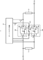
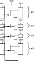
- FIG. 3 is a plan view illustrating an outline of a transistor package PKG1 according to the first embodiment.
- FIG. 6 is a diagram illustrating a configuration example of a Doherty amplifier circuit according to a second embodiment.
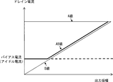
- FIG. It is a figure which shows the relationship between the output amplitude and drain current of the amplifier circuit of each class.
- FIG. 10 is a diagram illustrating a first specific configuration example of the Doherty amplifier circuit according to the second embodiment.
- FIG. 10 is a diagram illustrating a second specific configuration example of the Doherty amplifier circuit according to the second embodiment.
- FIG. 10 is a diagram illustrating a third specific configuration example of the Doherty amplifier circuit according to the second embodiment.
- FIG. 10 is a diagram illustrating a fourth specific configuration example of the Doherty amplifier circuit according to the second embodiment.
- FIG. 10 is a diagram illustrating a fifth specific configuration example of the Doherty amplifier circuit according to the second embodiment.
- FIG. 6 is a diagram illustrating a first configuration example of a Doherty amplifier circuit according to a third embodiment.
- FIG. 10 is a diagram illustrating a second configuration example of the Doherty amplifier circuit according to the third embodiment.
- FIG. 10 is a diagram illustrating a third configuration example of the Doherty amplifier circuit according to the third embodiment.
- FIG. 10 is a diagram illustrating a fourth configuration example of the Doherty amplifier circuit according to the third embodiment.
- FIG. 10 is a diagram illustrating a fifth configuration example of the Doherty amplifier circuit according to the third embodiment.
- FIG. 14 is a diagram showing a relationship between power and power efficiency of the Doherty amplifier circuit shown in FIGS. 10 to 13;
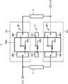
- FIG. 10 is a plan view showing an outline of a transistor package PKG2 according to a fourth embodiment.
- FIG. 16 is a diagram for describing a Doherty amplifier circuit to which the transistor package PKG2 illustrated in FIG. 15 is applied.
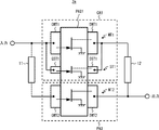
- FIG. 10 is a plan view illustrating an outline of a transistor package PKG3 according to a fourth embodiment.
- FIG. 18 is a diagram for describing a Doherty amplifier circuit to which the transistor package PKG3 illustrated in FIG. 17 is applied.
- the constituent elements are not necessarily essential unless otherwise specified or apparently essential in principle.
- the shapes when referring to the shapes, positional relationships, etc. of the components, etc., the shapes are substantially the same unless otherwise specified, or otherwise apparent in principle. And the like are included. The same applies to the above numbers and the like (including the number, numerical value, quantity, range, etc.).
- FIG. 1 is a plan view schematically showing the transistor package PKG1 according to the first embodiment.
- a transistor package PKG1 shown in FIG. 1 is a transistor package including a plurality of transistors for constituting a Doherty amplifier circuit or the like, and includes a main transistor (first main transistor) MT1 and a main transistor (second main transistor) MT2. And a sub-transistor (first sub-transistor) ST1.
- the main transistors MT1 and MT2 and the sub-transistor ST1 are all N-channel field effect transistors will be described as an example.
- the sub-transistor ST1 is disposed at the center of the package in plan view, and the main transistors MT1 and MT2 are disposed near both ends of the package with the sub-transistor ST1 interposed therebetween.
- the arrangement positions of the main transistors MT1 and MT2 and the sub-transistor ST1 are not limited to the arrangement positions shown in FIG.
- one of the main transistors MT1 and MT2 may be arranged in the center of the package instead of the sub-transistor ST1.
- the size of the sub-transistor ST1 is smaller than the size of the main transistors MT1 and MT2.
- the gate width Wa of the sub-transistor ST1 is smaller than the gate width Wb of the main transistors MT1 and MT2.
- the size of the sub-transistor ST1 is about 1/2 to 1/20 of the size of the main transistors MT1 and MT2.
- the drain electrode DMT1 and the gate electrode GMT1 of the main transistor MT1, the drain electrode DMT2 and the gate electrode GMT2 of the main transistor MT2, and the drain electrode DST1 and the gate electrode GST1 of the sub-transistor ST1 are extended from the transistor package PKG1. Is provided. Note that the sources of the main transistors MT1 and MT2 and the sub-transistor ST1 are grounded.
- the transistor package PKG1 shown in FIG. 1 can constitute various types of Doherty amplifier circuits such as a Doherty amplifier circuit to which an auto-bias function is added and an extended Doherty amplifier circuit.
- Doherty amplifier circuits such as a Doherty amplifier circuit to which an auto-bias function is added and an extended Doherty amplifier circuit.
- the size of the sub-transistor ST1 is small in the transistor package PKG1 shown in FIG. 1, various types of Doherty amplifier circuits can be realized on a small scale.
- the main transistors MT1 and MT2 and the sub-transistor ST1 preferably have substantially the same DC characteristics and high-frequency characteristics per unit gate width.
- the main transistors MT1 and MT2 and the sub-transistor ST1 are formed of the same die, so that the direct current characteristics and the high frequency characteristics per unit gate width have substantially the same characteristics.
- the performance of the Doherty amplifier circuit to which the transistor package PKG1 is applied can be improved.
- a desired bias can be given to each transistor with higher accuracy while suppressing variations.
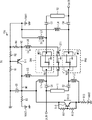
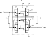
- FIG. 2 is a diagram illustrating a configuration example of the Doherty amplifier circuit 1 according to the second embodiment.
- the Doherty amplifier circuit 1 illustrated in FIG. 2 includes a carrier amplifier (first amplifier) CA1, a peak amplifier (second amplifier) PA1, an auto bias circuit 10, a distributor 11, and a combiner 12.
- the matching circuit, the bypass capacitor, and the like are omitted for simplification.
- the distributor 11 distributes the input signal and generates first and second distribution signals.
- the distributor 11 adjusts the phase of the input signal so that the phases of the output signals of the carrier amplifier CA1 and the peak amplifier PA1 are in phase when they are combined by the combiner 12.
- a second distribution signal is generated.
- the distributor 11 is configured by a 1/4 wavelength transmission line, a 90 ° hybrid circuit, or the like.
- the carrier amplifier CA1 includes a main transistor MT1 provided in the transistor package PKG1, amplifies the first distribution signal input to the gate of the main transistor MT1, and outputs the amplified signal from the drain of the transistor MT1.
- the carrier amplifier CA1 is biased to, for example, class AB or class B, and linearly amplifies the first distribution signal.
- the peak amplifier PA1 includes a main transistor MT2 provided in the transistor package PKG1, amplifies the second distribution signal input to the gate of the main transistor MT2, and outputs the amplified signal from the drain of the transistor MT2.
- the peak amplifier PA1 is biased to, for example, class C, and nonlinearly amplifies the second distribution signal. That is, the peak amplifier PA1 performs an amplification operation only at the time of high power output.
- the combiner 12 combines the output signals of the carrier amplifier CA1 and the peak amplifier PA1 and outputs the combined signals as output signals of the Doherty amplifier circuit 1.
- the synthesizer 12 is usually composed of a transformer, an impedance converter, or a transmission path of 1/4 wavelength or the like when handling a signal such as a microwave band.
- the Doherty amplifier circuit 1 includes a carrier amplifier CA1 that operates while maintaining saturation near the saturated output power, and a peak amplifier PA1 that operates only near the saturated output power, thereby taking back-off from the saturated power. Even at the time of output, higher power efficiency is realized than a normal class A or class AB amplifier circuit.
- the carrier amplifier CA1 and the peak amplifier PA1 are built in one package. Therefore, the Doherty amplifier circuit 1 can be downsized as compared with the configuration in which the carrier amplifier CA1 and the peak amplifier PA1 are incorporated in different packages. In addition, since the transmission line length from the output of each of the carrier amplifier CA1 and the peak amplifier PA1 to the signal combining point in the combiner 12 is shortened, the transmission loss is reduced. As a result, the power efficiency of the Doherty amplifier circuit 1 is improved. be able to.
- the auto bias circuit 10 is a circuit that automatically sets a bias current and a bias voltage for each of the carrier amplifier CA1 and the peak amplifier PA1. Although not shown in FIG. 2, in practice, the auto bias circuit 10 operates by providing a DC blocking capacitor on the input / output signal line of each amplifier. A specific configuration example of the auto bias circuit 10 will be described later with reference to FIG.
- the auto-bias circuit 10 detects the gate voltage of the sub-transistor ST1 that keeps the drain current (bias current) of the sub-transistor ST1 at a predetermined value Ia.
- the auto bias circuit 10 supplies a bias voltage Vb1 corresponding to the detected gate voltage (in this example, the detected gate voltage is directly used as the bias voltage Vb1) to the gate of the main transistor MT1.
- the drain current (bias current) of the main transistor MT1 constituting the carrier amplifier CA1 is set to the desired value Ib.
- the bias voltage Vb1 is set to a bias voltage value at which the carrier amplifier CA1 operates as a class AB or class B amplifier.
- the bias current of the sub-transistor ST1 is Ia and the bias current of the main transistor MT1 is Ib
- the auto bias circuit 10 supplies a bias voltage Vb2 corresponding to the detected gate voltage to the gate of the main transistor MT2.
- the auto bias circuit 10 generates a bias voltage Vb2 having a voltage level lower than the bias voltage Vb1 by subtracting the voltage from the bias voltage Vb1 using the voltage addition / subtraction unit 13.
- the drain current (bias current) of the main transistor MT2 constituting the peak amplifier PA1 is set to a desired value.
- the bias voltage Vb2 is set to a bias voltage value at which the peak amplifier PA1 operates as a class C amplifier.
- FIG. 3 is a diagram showing the relationship between the output amplitude and drain current of each class of amplifier circuits.
- the carrier amplifier CA1 is biased to, for example, the class AB in which the drain current increases as the output amplitude increases.
- the auto bias circuit 10 is configured to supply the bias voltage Vb1 directly to the gate of the main transistor MT1, the drain current of the carrier amplifier CA1 has the auto bias circuit 10 even if the output amplitude increases. It is held at a constant value by the desired negative feedback action (dotted line in FIG. 3). Therefore, the carrier amplifier CA1 cannot perform a desired amplification operation.
- a current detection element such as a resistance element is provided between the power supply and the drain of the carrier amplifier CA1 in order to detect the drain current. Therefore, power consumption increases due to this current detection element.
- the auto bias circuit 10 detects and sets the bias voltage Vb1 (Vb2) using the sub-transistor ST1.
- the bias voltage Vb1 is not changed by the signal input / output. That is, the bias voltage Vb1 of the carrier amplifier CA1 is maintained at a desired value by the auto bias circuit 10 regardless of signal input / output. Therefore, the drain current of the carrier amplifier CA1 is not held at a constant value even when the output amplitude increases (solid line in FIG. 3). Therefore, the carrier amplifier CA1 can perform a desired amplification operation.
- the size of the sub-transistor ST1 is small, even when a current detection element such as a resistance element is provided between the power supply and the drain of the sub-transistor ST1, the power consumed by the current detection element can be reduced. Is possible.
- a Doherty amplifier circuit to which an auto-bias function is added can be configured using the transistor package PKG1.
- the size of the sub-transistor ST1 is small in the transistor package PKG1, a Doherty amplifier circuit to which an auto-bias function is added can be realized on a small scale.
- the transmission line length from the output of each of the carrier amplifier CA1 and the peak amplifier PA1 to the signal synthesis point is shortened, the transmission loss is reduced. As a result, the power efficiency of the Doherty amplifier circuit 1 can be improved.
- the gate voltage of the sub-transistor ST1 may be used, for example, for bias setting of a driver or pre-driver with a very small output power provided in the previous stage of the Doherty amplifier circuit 1.
- very small refers to a region where the drain current can be regarded as substantially constant regardless of the output power in the vicinity of the operating point. Since part of the power consumed by the auto-bias circuit 10 can be used for the bias setting of the driver or pre-driver, the power efficiency of the entire amplifier circuit can be further improved.
- the driver or the pre-driver may have, for example, a configuration of a Doherty amplifier circuit with an auto bias function as shown in FIG.
- the configuration of the auto-bias circuit 10 shown in FIG. 2 is only an example for explaining the operation principle of the present invention, and can be appropriately changed to another configuration having an equivalent function. Several specific examples will be described below.
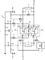
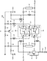
- FIG. 4 is a diagram illustrating a first specific configuration example of the Doherty amplifier circuit 1.
- FIG. 4 shows a specific configuration example of the auto bias circuit 1.
- the auto-bias circuit 10 shown in FIG. 4 includes capacitive elements C1 to C5, coils L1 to L6, resistance elements R1 to R4, a voltage addition / subtraction unit 13, a bipolar transistor Tr1, and a sub-transistor provided in the transistor package PKG1. ST1.
- the coils L1 to L6 mean RF choke coils.
- the resistance elements R1 and R2 are provided in series between the ground voltage terminal GND and the power supply voltage terminal Vdd1.
- the base is connected to the node between the resistance elements R1 and R2, the collector is connected to the node N1, and the emitter is connected to the node N2.
- Resistance element R3 is provided between power supply voltage terminal Vdd2 and node N1.
- Resistance element R4 is provided between power supply voltage terminal Vdd1 and node N2.
- the capacitive element C1 is provided between a node between the external input terminal of the Doherty amplifier circuit 1 and the input terminal of the distributor 11, and an input terminal of the carrier amplifier CA1 (gate electrode of the transistor MT1).
- the capacitive element C2 is provided between the output terminal of the distributor 11 and the input terminal of the peak amplifier PA1 (the gate electrode of the transistor MT2).
- the capacitive element C3 is provided between the output terminal of the carrier amplifier CA1 (the drain electrode of the transistor MT1) and the input terminal of the combiner 12.
- the capacitive element C4 is provided between the output terminal of the peak amplifier PA1 (the drain electrode of the transistor MT2) and a node between the external output terminal of the Doherty amplifier circuit 1 and the output terminal of the combiner 12.
- the capacitive element C5 is provided between the ground voltage terminal GND and the node N1.
- the coil L1 is provided between the input terminal of the carrier amplifier CA1 and the node N1.
- the coil L2 is provided between the input terminal of the peak amplifier PA1 and the node N1.
- the coil L3 is provided between the output terminal of the carrier amplifier CA1 and the power supply voltage terminal Vdd1.
- the coil L4 is provided between the output terminal of the peak amplifier PA1 and the power supply voltage terminal Vdd1.
- the coil L5 is provided between the gate electrode of the sub-transistor ST1 and the node N1.
- the coil L6 is provided between the drain electrode of the sub-transistor ST1 and the node N2.
- the voltage addition / subtraction unit 13 is provided between the coil L2 and the node N1.
- the gate bias can be wired by RF choking in the package.
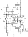
- FIG. 5 is a diagram illustrating a second specific configuration example of the Doherty amplifier circuit 1 as the Doherty amplifier circuit 1a.
- the Doherty amplifier circuit 1a shown in FIG. 5 includes N (N is a natural number) diodes D1 to DN and a resistance element R13 as a voltage addition / subtraction unit 13. .
- the diodes D1 to DN are provided in series between the node N1 and the coil L2.
- the anodes of the diodes D1 to DN are connected to the node N1 side, and the cathodes of the diodes D1 to N are connected to the coil L2 side.
- the resistance element R13 is provided between a node between the diodes D1 to DN and the coil L2, and the power supply voltage terminal Vdd3.
- Vf the relationship between the bias voltages Vb1 and Vb2
- Vb2 Vb1 ⁇ N ⁇ Vf. Since the voltage drop per diode is about 0.7V, for example, when the number of diodes is 3, the potential difference generated between the bias voltages Vb1 and Vb2 is about 2.1V. Of course, it may be used in combination with diodes having different degrees of voltage drop.
- FIG. 6 is a diagram illustrating a third specific configuration example of the Doherty amplifier circuit 1 as the Doherty amplifier circuit 1b.
- the Doherty amplifier circuit 1b shown in FIG. 6 includes a Zener diode ZD1 and a resistance element R13 as the voltage adder / subtractor 13 as compared with the Doherty amplifier circuit 1 shown in FIG.
- the cathode of the Zener diode ZD1 is connected to the node N1, and the anode of the Zener diode ZD1 is connected to the coil L2.
- the resistance element R13 is provided between a node between the Zener diode ZD1 and the coil L2 and the power supply voltage terminal Vdd3.
- Vb2 Vb1 ⁇ Vzd.
- FIG. 7 is a diagram illustrating a fourth specific configuration example of the Doherty amplifier circuit 1 as the Doherty amplifier circuit 1c.
- the Doherty amplifier circuit 1c shown in FIG. 7 includes an NPN bipolar transistor Tr2 and resistance elements R11 to R13 as the voltage addition / subtraction unit 13.
- the collector of the bipolar transistor Tr2 is connected to the node N1, and the emitter of the bipolar transistor Tr2 is connected to the coil L2.
- the resistance element R11 is provided between the base and collector of the bipolar transistor Tr2.
- the resistance element R12 is provided between the base and emitter of the bipolar transistor Tr2.
- the resistance element R13 is provided between the emitter of the bipolar transistor Tr2 and the power supply voltage terminal Vdd3.
- Vtr2 Vb1 ⁇ Vtr2.
- the base-emitter voltage of the bipolar transistor Tr2 Vbe, then Vtr2 ⁇ (1 + R11 / R12) ⁇ Vbe.
- FIG. 8 is a diagram illustrating a fifth specific configuration example of the Doherty amplifier circuit 1 as the Doherty amplifier circuit 1d.
- the Doherty amplifier circuit 1d shown in FIG. 8 includes a PNP-type bipolar transistor Tr3 and resistance elements R11 to R13 as the voltage addition / subtraction unit 13.
- the emitter of the bipolar transistor Tr3 is connected to the node N1, and the collector of the bipolar transistor Tr3 is connected to the coil L2.
- the resistance element R11 is provided between the base and emitter of the bipolar transistor Tr3.
- the resistance element R12 is provided between the base and collector of the bipolar transistor Tr3.
- the resistance element R13 is provided between the collector of the bipolar transistor Tr3 and the power supply voltage terminal Vdd3.
- the voltage adding / subtracting unit 13 shown in FIGS. 5 to 8 are all simple, for example, together with all or part of the auto-bias circuit 10, the main transistors MT1 and MT2, and the sub-transistor ST1. It can be integrated or mounted in the same package. Of course, a circuit for compensating the temperature characteristics of the diode may be further provided.
- an extended Doherty amplifier circuit will be described as another example of the Doherty amplifier circuit to which the transistor package PKG1 illustrated in FIG. 1 is applied.
- FIG. 9 is a diagram illustrating a first configuration example of the Doherty amplifier circuit 2 according to the third embodiment.
- the Doherty amplifier circuit 2 shown in FIG. 9 includes a carrier amplifier CA1, a peak amplifier PA1, a distributor 11, and a combiner 12. Since the basic operation and connection relationship of each component are as described above, description thereof is omitted.
- the carrier amplifier CA1 is constituted by a transistor MT1
- the peak amplifier PA1 is constituted by a transistor MT2. That is, the carrier amplifier CA1 and the peak amplifier PA1 are composed of transistors having the same size. Therefore, in the Doherty amplifier circuit 2 shown in FIG. 9, the power distributed to each of the carrier amplifier CA1 and the peak amplifier PA1 is the same.
- FIG. 10 is a diagram illustrating a second configuration example of the Doherty amplifier circuit 2 according to the third embodiment as the Doherty amplifier circuit 2a.
- the Doherty amplifier circuit 2a shown in FIG. 10 differs from the Doherty amplifier circuit 2 shown in FIG. 9 in the configuration of the carrier amplifier CA1.
- the carrier amplifier CA1 shown in FIG. 10 includes a main transistor MT1 and a sub-transistor ST1, and amplifies the first distribution signal input to the gates of the transistors MT1 and ST1, and from the drains of the transistors MT1 and ST1. Output.
- the other configuration of the Doherty amplifier circuit 2a shown in FIG. 10 is the same as that of the Doherty amplifier circuit 2 shown in FIG.
- the Doherty amplifier circuit 2a shown in FIG. 10 the power distributed to the carrier amplifier CA1 and the peak amplifier PA1 is different. That is, the Doherty amplifier circuit 2a shown in FIG. 10 constitutes a so-called extended Doherty amplifier circuit.
- FIG. 11 is a diagram illustrating a third configuration example of the Doherty amplifier circuit 2 according to the third embodiment as the Doherty amplifier circuit 2b.
- the arrangement of the carrier amplifier CA1 and the peak amplifier PA1 is switched compared to the Doherty amplifier circuit 2a shown in FIG.
- the carrier amplifier CA1 shown in FIG. 11 includes a main transistor MT2 and a sub-transistor ST1, and amplifies the first distribution signal input to the gates of the transistors MT2 and ST1, and from the drains of the transistors MT2 and ST1. Output.
- a peak amplifier PA1 shown in FIG. 11 includes a main transistor MT1, amplifies the second distribution signal input to the gate of the main transistor MT1, and outputs the amplified signal from the drain of the main transistor MT1. Since the other configuration of the Doherty amplifier circuit 2b shown in FIG. 11 is the same as that of the Doherty amplifier circuit 2 shown in FIG. 9, the description thereof is omitted.
- the Doherty amplifier circuit 2b shown in FIG. 11 power is distributed to each of the carrier amplifier CA1 and the peak amplifier PA1 at the same ratio as the Doherty amplifier circuit 2a shown in FIG. That is, the Doherty amplifier circuit 2b shown in FIG. 11 configures an extended Doherty amplifier circuit similar to the Doherty amplifier circuit 2a shown in FIG. 10 except that the arrangement of the carrier amplifier CA1 and the peak amplifier PA1 is switched. Yes.
- FIG. 12 is a diagram illustrating a fourth configuration example of the Doherty amplifier circuit 2 according to Embodiment 3 as the Doherty amplifier circuit 2c.
- the Doherty amplifier circuit 2c shown in FIG. 12 differs from the Doherty amplifier circuit 2 shown in FIG. 9 in the configuration of the peak amplifier PA1.
- the peak amplifier PA1 shown in FIG. 12 includes a main transistor MT2 and a sub-transistor ST1, and amplifies the second distribution signal input to the gates of the transistors MT2 and ST1, and from the drains of the transistors MT2 and ST1. Output. Since the other configuration of the Doherty amplifier circuit 2c shown in FIG. 12 is the same as that of the Doherty amplifier circuit 2 shown in FIG. 9, the description thereof is omitted.
- the Doherty amplifier circuit 2c shown in FIG. 12 the power distributed to the carrier amplifier CA1 and the peak amplifier PA1 is different. That is, the Doherty amplifier circuit 2c shown in FIG. 12 constitutes a so-called extended Doherty amplifier circuit.
- FIG. 13 is a diagram illustrating a fifth configuration example of the Doherty amplifier circuit 2 according to the third embodiment as the Doherty amplifier circuit 2d.
- the arrangement of the carrier amplifier CA1 and the peak amplifier PA1 is switched compared to the Doherty amplifier circuit 2c shown in FIG.
- the carrier amplifier CA1 shown in FIG. 13 includes a main transistor MT2, amplifies the first distribution signal input to the gate of the main transistor MT2, and outputs it from the drain of the main transistor MT2.
- a peak amplifier PA1 shown in FIG. 13 includes a main transistor MT1 and a sub-transistor ST1, and amplifies the second distribution signal input to the gates of the transistors MT1 and ST1 and outputs the amplified signal from the drains of the transistors MT1 and ST1.
- the other configuration of the Doherty amplifier circuit 2d shown in FIG. 13 is the same as that of the Doherty amplifier circuit 2 shown in FIG.
- the Doherty amplifier circuit 2d shown in FIG. 13 power is distributed to each of the carrier amplifier CA1 and the peak amplifier PA1 at the same ratio as in the Doherty amplifier circuit 2c shown in FIG. That is, the Doherty amplifier circuit 2d shown in FIG. 13 constitutes an extended Doherty amplifier circuit similar to the Doherty amplifier circuit 2c shown in FIG. 12, except that the arrangement of the carrier amplifier CA1 and the peak amplifier PA1 is switched. Yes.
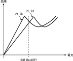
- FIG. 14 is a diagram showing the relationship between the power and power efficiency of the Doherty amplifier circuits 2a to 2d shown in FIGS. As shown in FIG. 14, it can be seen that the Doherty amplifier circuits 2a and 2b and the Doherty amplifier circuits 2c and 2d having different power distribution ratios with respect to the carrier amplifier CA1 and the peak amplifier PA1 have different power efficiency peaks with respect to power. That is, an extended Doherty amplifier circuit having various operating characteristics can be configured using the transistor package PKG1.
- an extended Doherty amplifier circuit having a desired operation characteristic and a desired arrangement can be configured by using the transistor package PKG1.
- the size of the sub-transistor ST1 is small in the transistor package PKG1, an extended Doherty amplifier circuit having a desired operation characteristic and a desired arrangement can be realized on a small scale. Further, if the number of sub-transistors ST1 is increased, the power distribution ratio can be finely adjusted.
- the transmission line length from the output of each of the carrier amplifier CA1 and the peak amplifier PA1 to the signal synthesis point is shortened, the transmission loss is reduced. As a result, the power efficiency of the extended Doherty amplifier circuit can be improved.
- FIG. 15 is a plan view schematically showing a transistor package PKG2 according to the fourth embodiment.
- the transistor package PKG2 illustrated in FIG. 15 further includes a sub-transistor (second sub-transistor) ST2 having the same structure as the sub-transistor ST1 as compared with the transistor package PKG1 illustrated in FIG.
- Other configurations of the transistor package PKG2 illustrated in FIG. 15 are the same as those of the transistor package PKG1 illustrated in FIG.
- the main transistor MT1, the sub-transistor ST1, the main transistor MT2, and the sub-transistor ST1 are arranged in the order in the package.
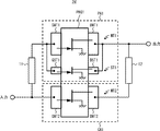
- FIG. 16 is a diagram for explaining a Doherty amplifier circuit to which the transistor package PKG2 shown in FIG. 15 is applied.
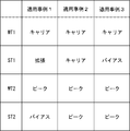
- FIG. 16 shows three application examples of the transistor package PKG2 shown in FIG.
- “carrier” in the figure indicates that the transistor constitutes the carrier amplifier CA1
- “peak” indicates that the transistor constitutes the peak amplifier PA1
- “bias” indicates that the transistor is an auto-bias circuit.
- 10 indicates that the transistor constitutes a carrier amplifier CA1 or a peak amplifier PA1 together with other main transistors. Note that the three application examples shown in FIG. 16 are merely examples.
- FIG. 17 is a plan view showing a modified example of the transistor package PKG2 according to the present embodiment as a transistor package PKG3.
- the arrangement positions of the transistors are different from those of the transistor package PKG2 illustrated in FIG.
- the main transistor MT1, the subtransistor ST1, the subtransistor ST1, and the main transistor MT2 are arranged in the package in order in plan view.
- FIG. 18 is a diagram for explaining a Doherty amplifier circuit to which the transistor package PKG3 shown in FIG. 17 is applied. 18 shows four application examples of the transistor package PKG3 shown in FIG.
- the transistor packages PKG2 and PKG3 include the two sub-transistors ST1 and ST2, more various types of Doherty amplifier circuits such as an extended Doherty amplifier circuit to which an auto bias function is added are configured. Can do.
- the sizes of the sub-transistors ST1 and ST2 are small in the transistor packages PKG2 and PKG3, various types of Doherty amplifier circuits can be realized on a small scale.
- the number of sub-transistors provided in the transistor package PKG2 may be three or more.
- the number of main transistors provided in the transistor package PKG2 may be three or more.
- the transistor packages PKG1 to PKG3 include various types of Doherty amplifier circuits such as a Doherty amplifier circuit to which an auto-bias function is added and an extended Doherty amplifier circuit having desired operation characteristics. Can be configured. Since various types of Doherty amplifier circuits can be configured by a common transistor package, when various types of Doherty amplifier circuits are designed and manufactured, it is possible to reduce the design man-hours and management adjustment man-hours to increase efficiency. Here, since the transistor packages PKG1 and PKG2 have small sub-transistor sizes, various types of Doherty amplifier circuits can be realized on a small scale.
- the main transistors MT1 and MT2 and the sub-transistors ST1 and ST2 are field effect transistors
- the main transistors MT1, MT2 and subtransistors ST1, ST2 may be bipolar transistors.
- the size of the field effect transistor is typically represented by the gate width, whereas the size of the bipolar transistor is represented by the emitter area.
- a field effect transistor is a voltage control element
- a bipolar transistor is a current control element. Therefore, when a bipolar transistor is used, a bias or the like is given by a current. It goes without saying that the present invention can be realized by making an easy change.
- the transistor packages PKG1 to PKG3 may be configured with the sizes of the sub-transistors ST1 and ST2 being approximately the same as the sizes of the main transistors MT1 and MT2.
Landscapes
- Engineering & Computer Science (AREA)
- Power Engineering (AREA)
- Microelectronics & Electronic Packaging (AREA)
- Amplifiers (AREA)
Abstract
Description
図1は、実施の形態1に係るトランジスタパッケージPKG1の概略を示す平面図である。図1に示すトランジスタパッケージPKG1は、ドハティ増幅回路等を構成するための複数のトランジスタを備えたトランジスタパッケージであって、メイントランジスタ(第1メイントランジスタ)MT1と、メイントランジスタ(第2メイントランジスタ)MT2と、サブトランジスタ(第1サブトランジスタ)ST1と、を備える。なお、本実施の形態では、メイントランジスタMT1,MT2及びサブトランジスタST1が何れもNチャネル型の電界効果トランジスタである場合を例に説明する。
本実施の形態では、図1に示すトランジスタパッケージPKG1が適用されたドハティ増幅回路の一例として、オートバイアス機能が付加されたドハティ増幅回路について説明する。
分配器11は、入力信号を分配して第1及び第2分配信号を生成する。分配器11は、キャリア増幅器CA1及びピーク増幅器PA1のそれぞれの出力信号が合成器12にて合成されるときに、それらの位相が同相となるように、入力信号の位相を調整して第1及び第2分配信号を生成する。例えば、分配器11は、1/4波長の伝送線路や90°ハイブリッド回路などによって構成されている。
キャリア増幅器CA1は、トランジスタパッケージPKG1に設けられたメイントランジスタMT1により構成され、メイントランジスタMT1のゲートに入力された第1分配信号を増幅してトランジスタMT1のドレインから出力する。ここで、キャリア増幅器CA1は、例えば、AB級やB級にバイアスされ、第1分配信号を線形増幅する。
ピーク増幅器PA1は、トランジスタパッケージPKG1に設けられたメイントランジスタMT2により構成され、メイントランジスタMT2のゲートに入力された第2分配信号を増幅してトランジスタMT2のドレインから出力する。ここで、ピーク増幅器PA1は、例えば、C級にバイアスされ、第2分配信号を非線形増幅する。つまり、ピーク増幅器PA1は、高電力出力時にのみ増幅動作を行う。
合成器12は、キャリア増幅器CA1及びピーク増幅器PA1のそれぞれの出力信号を合成し、ドハティ増幅回路1の出力信号として出力する。例えば、合成器12は、トランス、インピーダンス変換器、又は、マイクロ波帯等の信号を扱う場合には通常1/4波長の伝送経路等によって構成されている。
オートバイアス回路10は、キャリア増幅器CA1及びピーク増幅器PA1のそれぞれに対して自動でバイアス電流やバイアス電圧を設定する回路である。なお、図2には示されていないが、実際には、各増幅器の入出力信号線上に直流遮断用のキャパシタが設けられることでオートバイアス回路10は動作する。オートバイアス回路10の具体的な構成例については、図4等を用いて後述する。
図4は、ドハティ増幅回路1の第1具体的構成例を示す図である。図4では、オートバイアス回路1の具体的構成例が示されている。
図5は、ドハティ増幅回路1の第2具体的構成例をドハティ増幅回路1aとして示す図である。図5に示すドハティ増幅回路1aは、図4に示すドハティ増幅回路1と比較して、電圧加減算部13として、N(Nは自然数)個のダイオードD1~DNと、抵抗素子R13と、を備える。
図6は、ドハティ増幅回路1の第3具体的構成例をドハティ増幅回路1bとして示す図である。図6に示すドハティ増幅回路1bは、図4に示すドハティ増幅回路1と比較して、電圧加減算部13として、ツェナーダイオードZD1と、抵抗素子R13と、を備える。
図7は、ドハティ増幅回路1の第4具体的構成例をドハティ増幅回路1cとして示す図である。図7に示すドハティ増幅回路1cは、図4に示すドハティ増幅回路1と比較して、電圧加減算部13として、NPN型のバイポーラトランジスタTr2と、抵抗素子R11~R13と、を備える。
図8は、ドハティ増幅回路1の第5具体的構成例をドハティ増幅回路1dとして示す図である。図8に示すドハティ増幅回路1dは、図4に示すドハティ増幅回路1と比較して、電圧加減算部13として、PNP型のバイポーラトランジスタTr3と、抵抗素子R11~R13と、を備える。
本実施の形態では、図1に示すトランジスタパッケージPKG1が適用されたドハティ増幅回路の他の例として、拡張型ドハティ増幅回路について説明する。
図9は、実施の形態3に係るドハティ増幅回路2の第1構成例を示す図である。図9に示すドハティ増幅回路2は、キャリア増幅器CA1と、ピーク増幅器PA1と、分配器11と、合成器12と、を備える。各構成要素の基本動作及び接続関係については、前述のとおりであるため、その説明を省略する。
図10は、実施の形態3に係るドハティ増幅回路2の第2構成例をドハティ増幅回路2aとして示す図である。図10に示すドハティ増幅回路2aでは、図9に示すドハティ増幅回路2と比較して、キャリア増幅器CA1の構成が異なる。
図11は、実施の形態3に係るドハティ増幅回路2の第3構成例をドハティ増幅回路2bとして示す図である。図11に示すドハティ増幅回路2bでは、図10に示すドハティ増幅回路2aと比較して、キャリア増幅器CA1及びピーク増幅器PA1の配置が入れ替わっている。
図12は、実施の形態3に係るドハティ増幅回路2の第4構成例をドハティ増幅回路2cとして示す図である。図12に示すドハティ増幅回路2cでは、図9に示すドハティ増幅回路2と比較して、ピーク増幅器PA1の構成が異なる。
図13は、実施の形態3に係るドハティ増幅回路2の第5構成例をドハティ増幅回路2dとして示す図である。図13に示すドハティ増幅回路2dでは、図12に示すドハティ増幅回路2cと比較して、キャリア増幅器CA1及びピーク増幅器PA1の配置が入れ替わっている。
図15は、実施の形態4に係るトランジスタパッケージPKG2の概略を示す平面図である。図15に示すトランジスタパッケージPKG2は、図1に示すトランジスタパッケージPKG1と比較して、サブトランジスタST1と同じ構造のサブトランジスタ(第2サブトランジスタ)ST2をさらに備える。図15に示すトランジスタパッケージPKG2のその他の構成については、図1に示すトランジスタパッケージPKG1の場合と同様であるため、その説明を省略する。
図17は、本実施の形態に係るトランジスタパッケージPKG2の変形例をトランジスタパッケージPKG3として示す平面図である。図17に示すトランジスタパッケージPKG3では、図15に示すトランジスタパッケージPKG2と比較して、各トランジスタの配置位置が異なる。
1a~1d ドハティ増幅回路
2 ドハティ増幅回路
2a~2d ドハティ増幅回路
10 オートバイアス回路
10a~10d オートバイアス回路
11 分配器
12 合成器
13 電圧加減算部
13a~13d 電圧加減算部
C1~C5 容量素子
CA1 キャリア増幅器
D1~DN ダイオード
DMT1 ドレイン電極
DMT2 ドレイン電極
DST1 ドレイン電極
DST2 ドレイン電極
GMT1 ゲート電極
GMT2 ゲート電極
GST1 ゲート電極
GST2 ゲート電極
L1~L6 コイル
MT1,MT2 メイントランジスタ
PA1 ピーク増幅器
PKG1~PKG3 トランジスタパッケージ
R1~R4 抵抗素子
R11~R13 抵抗素子
ST1,ST2 サブトランジスタ
Tr1~Tr3 バイポーラトランジスタ
ZD1 ツェナーダイオード
Claims (18)
- 第1及び第2メイントランジスタと、
前記第1及び前記第2メイントランジスタと同じパッケージ内に設けられ、前記第1及び前記第2メイントランジスタよりもサイズの小さい第1サブトランジスタと、を備えたトランジスタパッケージ。 - 請求項1に記載のトランジスタパッケージを備えた増幅回路であって、
入力信号を分配して第1及び第2分配信号を生成する分配器と、
少なくとも前記第1メイントランジスタにより構成され、前記第1分配信号を線形増幅する第1増幅器と、
少なくとも前記第2メイントランジスタにより構成され、前記第2分配信号を非線形増幅する第2増幅器と、
前記第1及び前記第2増幅器のそれぞれの出力信号を合成する合成器と、を備えた、増幅回路。 - 前記第1サブトランジスタは、前記第1又は前記第2メイントランジスタとともに、前記第1又は第2増幅器を構成する、請求項2に記載の増幅回路。
- 前記第1メイントランジスタ、前記第2メイントランジスタ及び前記第1サブトランジスタは、何れも電界効果トランジスタであって、
前記第1サブトランジスタのドレイン電流を所定値に保つような前記第1サブトランジスタのゲート電圧を検出し、検出された前記ゲート電圧に応じた第1バイアス電圧を前記第1メイントランジスタのゲートに供給することで前記第1増幅器の動作点を設定する、オートバイアス回路をさらに備えた、請求項2に記載の増幅回路。 - 前記オートバイアス回路は、さらに、検出された前記ゲート電圧に応じた第2バイアス電圧を前記第2メイントランジスタのゲートに供給することで前記第2増幅器の動作点を設定する、請求項4に記載の増幅回路。
- 前記第1メイントランジスタ、前記第2メイントランジスタ及び前記第1サブトランジスタは、何れもバイポーラトランジスタであって、
前記第1サブトランジスタのコレクタ電流を所定値に保つような前記第1サブトランジスタのベース電流を検出し、検出された前記ベース電流に応じた第1バイアス電流を前記第1メイントランジスタのベースに供給することで前記第1増幅器の動作点を設定する、オートバイアス回路をさらに備えた、請求項2に記載の増幅回路。 - 前記オートバイアス回路は、さらに、検出された前記ベース電流に応じた第2バイアス電流を前記第2メイントランジスタのベースに供給することで前記第2増幅器の動作点を設定する、請求項6に記載の増幅回路。
- 前記第1メイントランジスタ、前記第2メイントランジスタ及び前記第1サブトランジスタの単位サイズあたりの特性は略同一である、請求項2~7の何れか一項に記載の増幅回路。
- 前記第1及び前記第2メイントランジスタよりもサイズの小さい第2サブトランジスタをさらに備えた請求項1に記載のトランジスタパッケージ。
- 請求項9に記載のトランジスタパッケージを備えた増幅回路であって、
入力信号を分配して第1及び第2分配信号を生成する分配器と、
少なくとも前記第1メイントランジスタにより構成され、前記第1分配信号を線形増幅する第1増幅器と、
少なくとも前記第2メイントランジスタにより構成され、前記第2分配信号を非線形増幅する第2増幅器と、
前記第1及び前記第2増幅器のそれぞれの出力信号を合成する合成器と、を備えた、増幅回路。 - 前記第1サブトランジスタは、前記第1又は前記第2メイントランジスタとともに、前記第1又は第2増幅器を構成する、請求項10に記載の増幅回路。
- 前記第1メイントランジスタ、前記第2メイントランジスタ、前記第1サブトランジスタ及び前記第2サブトランジスタは、何れも電界効果トランジスタであって、
前記第2サブトランジスタのドレイン電流を所定値に保つような前記第2サブトランジスタのゲート電圧を検出し、検出された前記ゲート電圧に応じた第1バイアス電圧を前記第1メイントランジスタのゲートに供給することで前記第1増幅器の動作点を設定し、かつ、検出された前記ゲート電圧に応じた第2バイアス電圧を前記第2メイントランジスタのゲートに供給することで前記第2増幅器の動作点を設定する、オートバイアス回路をさらに備えた、請求項10又は11に記載の増幅回路。 - 前記第1メイントランジスタ、前記第2メイントランジスタ、前記第1サブトランジスタ及び前記第2サブトランジスタは、何れもバイポーラトランジスタであって、
前記第2サブトランジスタのコレクタ電流を所定値に保つような前記第2サブトランジスタのベース電流を検出し、検出された前記ベース電流に応じた第1バイアス電流を前記第1メイントランジスタのベースに供給することで前記第1増幅器の動作点を設定し、かつ、検出された前記ベース電流に応じた第2バイアス電流を前記第2メイントランジスタのベースに供給することで前記第2増幅器の動作点を設定する、オートバイアス回路をさらに備えた、請求項10又は11に記載の増幅回路。 - 前記第1メイントランジスタ、前記第2メイントランジスタ、前記第1サブトランジスタ及び第2サブトランジスタの単位サイズあたりの特性は略同一である、請求項10~13の何れか一項に記載の増幅回路。
- 前記サイズはゲート幅である、請求項1又は9に記載のトランジスタパッケージ。
- 前記サイズはゲート幅である、請求項2~8、10~14の何れか一項に記載の増幅回路。
- 第1及び第2メイントランジスタと、前記第1及び前記第2メイントランジスタよりもサイズの小さい第1サブトランジスタと、を同じパッケージ内に設ける、トランジスタの構成方法。
- 前記サイズはゲート幅である、請求項17に記載のトランジスタの構成方法。
Priority Applications (2)
| Application Number | Priority Date | Filing Date | Title |
|---|---|---|---|
| US15/112,912 US9853605B2 (en) | 2014-01-31 | 2014-10-10 | Transistor package, amplification circuit including the same, and method of forming transistor |
| JP2015559622A JPWO2015114698A1 (ja) | 2014-01-31 | 2014-10-10 | トランジスタパッケージ、それを備えた増幅回路、及び、トランジスタの構成方法 |
Applications Claiming Priority (2)
| Application Number | Priority Date | Filing Date | Title |
|---|---|---|---|
| JP2014-017171 | 2014-01-31 | ||
| JP2014017171 | 2014-01-31 |
Publications (1)
| Publication Number | Publication Date |
|---|---|
| WO2015114698A1 true WO2015114698A1 (ja) | 2015-08-06 |
Family
ID=53756324
Family Applications (1)
| Application Number | Title | Priority Date | Filing Date |
|---|---|---|---|
| PCT/JP2014/005161 Ceased WO2015114698A1 (ja) | 2014-01-31 | 2014-10-10 | トランジスタパッケージ、それを備えた増幅回路、及び、トランジスタの構成方法 |
Country Status (3)
| Country | Link |
|---|---|
| US (1) | US9853605B2 (ja) |
| JP (1) | JPWO2015114698A1 (ja) |
| WO (1) | WO2015114698A1 (ja) |
Cited By (2)
| Publication number | Priority date | Publication date | Assignee | Title |
|---|---|---|---|---|
| JP2022527051A (ja) * | 2019-03-28 | 2022-05-30 | ウルフスピード インコーポレイテッド | トランジスタ内負荷変調 |
| WO2023171364A1 (ja) * | 2022-03-10 | 2023-09-14 | 株式会社村田製作所 | 高周波モジュールおよび通信装置 |
Families Citing this family (3)
| Publication number | Priority date | Publication date | Assignee | Title |
|---|---|---|---|---|
| US9806681B2 (en) * | 2015-02-15 | 2017-10-31 | Skyworks Solutions, Inc. | Doherty power amplifier having AM-AM compensation |
| EP3723282B1 (en) * | 2019-04-12 | 2024-12-18 | NXP USA, Inc. | Power amplifier packages and systems incorporating design-flexible package platforms |
| CN114430884B (zh) | 2019-10-02 | 2024-11-12 | 三菱电机株式会社 | 多赫蒂放大器 |
Citations (4)
| Publication number | Priority date | Publication date | Assignee | Title |
|---|---|---|---|---|
| JPH1022300A (ja) * | 1996-07-08 | 1998-01-23 | Oki Electric Ind Co Ltd | 半導体集積回路 |
| JPH10270953A (ja) * | 1997-03-26 | 1998-10-09 | Mitsubishi Electric Corp | 高周波回路 |
| JP2005123861A (ja) * | 2003-10-16 | 2005-05-12 | Renesas Technology Corp | 高周波電力増幅回路および高周波電力増幅用電子部品 |
| JP2012500583A (ja) * | 2008-08-19 | 2012-01-05 | クリー インコーポレイテッド | 異なるターンオンパワーレベルを有するトランジスタ増幅器の並列な組を有する集積回路 |
Family Cites Families (10)
| Publication number | Priority date | Publication date | Assignee | Title |
|---|---|---|---|---|
| JP3265675B2 (ja) | 1993-02-09 | 2002-03-11 | 日本電気株式会社 | バイアス回路およびこれを用いた集積回路 |
| JP3444653B2 (ja) * | 1994-06-09 | 2003-09-08 | 三菱電機株式会社 | 電力増幅器 |
| JP5230044B2 (ja) * | 2000-08-28 | 2013-07-10 | 日本ケミコン株式会社 | 電気二重層コンデンサ |
| CN1853343B (zh) * | 2003-09-17 | 2012-01-11 | 日本电气株式会社 | 放大器 |
| US7304539B2 (en) | 2003-10-16 | 2007-12-04 | Renesas Technology Corporation | High frequency power amplifier circuit and electronic component for high frequency power amplifier |
| US7560983B1 (en) * | 2008-02-02 | 2009-07-14 | Zerog Wireless, Inc. | Multiple-path power amplifier |
| JP2011182043A (ja) * | 2010-02-26 | 2011-09-15 | Fujitsu Ltd | 増幅器 |
| WO2012083256A2 (en) * | 2010-12-17 | 2012-06-21 | Skyworks Solutions, Inc. | Apparatus and methods for oscillation suppression |
| EP2817880A4 (en) * | 2012-02-24 | 2015-05-20 | Ericsson Telefon Ab L M | REVERSE AMPLIFIER AND METHOD THEREFOR |
| JPWO2013153894A1 (ja) * | 2012-04-09 | 2015-12-17 | 三菱電機株式会社 | 増幅回路 |
-
2014
- 2014-10-10 WO PCT/JP2014/005161 patent/WO2015114698A1/ja not_active Ceased
- 2014-10-10 US US15/112,912 patent/US9853605B2/en not_active Expired - Fee Related
- 2014-10-10 JP JP2015559622A patent/JPWO2015114698A1/ja active Pending
Patent Citations (4)
| Publication number | Priority date | Publication date | Assignee | Title |
|---|---|---|---|---|
| JPH1022300A (ja) * | 1996-07-08 | 1998-01-23 | Oki Electric Ind Co Ltd | 半導体集積回路 |
| JPH10270953A (ja) * | 1997-03-26 | 1998-10-09 | Mitsubishi Electric Corp | 高周波回路 |
| JP2005123861A (ja) * | 2003-10-16 | 2005-05-12 | Renesas Technology Corp | 高周波電力増幅回路および高周波電力増幅用電子部品 |
| JP2012500583A (ja) * | 2008-08-19 | 2012-01-05 | クリー インコーポレイテッド | 異なるターンオンパワーレベルを有するトランジスタ増幅器の並列な組を有する集積回路 |
Cited By (4)
| Publication number | Priority date | Publication date | Assignee | Title |
|---|---|---|---|---|
| JP2022527051A (ja) * | 2019-03-28 | 2022-05-30 | ウルフスピード インコーポレイテッド | トランジスタ内負荷変調 |
| JP7383041B2 (ja) | 2019-03-28 | 2023-11-17 | ウルフスピード インコーポレイテッド | トランジスタ内負荷変調 |
| US12009788B2 (en) | 2019-03-28 | 2024-06-11 | Macom Technology Solutions Holdings, Inc. | In-transistor load modulation |
| WO2023171364A1 (ja) * | 2022-03-10 | 2023-09-14 | 株式会社村田製作所 | 高周波モジュールおよび通信装置 |
Also Published As
| Publication number | Publication date |
|---|---|
| JPWO2015114698A1 (ja) | 2017-03-23 |
| US20160344349A1 (en) | 2016-11-24 |
| US9853605B2 (en) | 2017-12-26 |
Similar Documents
| Publication | Publication Date | Title |
|---|---|---|
| US11855586B2 (en) | Power amplifier module | |
| TWI644511B (zh) | 電力增幅電路 | |
| JP6680235B2 (ja) | 電力増幅回路および高周波モジュール | |
| CN107408924B (zh) | 通过共射共基电流导引的增强的放大器效率 | |
| JP5821876B2 (ja) | 電力増幅モジュール | |
| US20150091645A1 (en) | Envelope tracking power transmitter using common-gate voltage modulation linearizer | |
| CN108933574B (zh) | 功率放大电路 | |
| CN110708026B (zh) | 改进效率的包络跟踪调制器的线性放大器 | |
| JP2010124433A (ja) | 高周波電力増幅器 | |
| KR102525526B1 (ko) | 베이스 전류를 재사용하는 증폭기 | |
| US9929694B2 (en) | Schottky enhanced bias circuit | |
| US7872532B2 (en) | High-frequency power amplifier and communication device | |
| JP7171950B2 (ja) | 電力増幅装置 | |
| WO2015114698A1 (ja) | トランジスタパッケージ、それを備えた増幅回路、及び、トランジスタの構成方法 | |
| JP4330549B2 (ja) | 高周波電力増幅装置 | |
| JP2025506139A (ja) | 包絡線追跡を用いて増幅器バイアスを調整するシステム及び方法 | |
| US20140354363A1 (en) | Power amplifier | |
| JP2010283556A (ja) | 高周波増幅器及びそれを用いた高周波モジュール | |
| JP2019205006A (ja) | 電力増幅回路 | |
| US20050140439A1 (en) | Predistortion linearizer for power amplifier | |
| JP2009094570A (ja) | 増幅器 | |
| KR101435342B1 (ko) | 이득을 부스팅하는 증폭기 | |
| JP2012065105A (ja) | 電力増幅器および無線機 | |
| CN116941180A (zh) | 基于输入信号包络跟踪调整放大器偏置电流的系统和方法 | |
| JP2007288736A (ja) | 電力増幅回路 |
Legal Events
| Date | Code | Title | Description |
|---|---|---|---|
| 121 | Ep: the epo has been informed by wipo that ep was designated in this application |
Ref document number: 14881264 Country of ref document: EP Kind code of ref document: A1 |
|
| ENP | Entry into the national phase |
Ref document number: 2015559622 Country of ref document: JP Kind code of ref document: A |
|
| WWE | Wipo information: entry into national phase |
Ref document number: 15112912 Country of ref document: US |
|
| NENP | Non-entry into the national phase |
Ref country code: DE |
|
| 122 | Ep: pct application non-entry in european phase |
Ref document number: 14881264 Country of ref document: EP Kind code of ref document: A1 |