WO2015111118A1 - 有機el表示装置および駆動方法 - Google Patents
有機el表示装置および駆動方法 Download PDFInfo
- Publication number
- WO2015111118A1 WO2015111118A1 PCT/JP2014/006372 JP2014006372W WO2015111118A1 WO 2015111118 A1 WO2015111118 A1 WO 2015111118A1 JP 2014006372 W JP2014006372 W JP 2014006372W WO 2015111118 A1 WO2015111118 A1 WO 2015111118A1
- Authority
- WO
- WIPO (PCT)
- Prior art keywords
- voltage
- organic
- switch
- electrode
- light emitting
- Prior art date
- Legal status (The legal status is an assumption and is not a legal conclusion. Google has not performed a legal analysis and makes no representation as to the accuracy of the status listed.)
- Ceased
Links
Images










Classifications
-
- G—PHYSICS
- G09—EDUCATION; CRYPTOGRAPHY; DISPLAY; ADVERTISING; SEALS
- G09G—ARRANGEMENTS OR CIRCUITS FOR CONTROL OF INDICATING DEVICES USING STATIC MEANS TO PRESENT VARIABLE INFORMATION
- G09G3/00—Control arrangements or circuits, of interest only in connection with visual indicators other than cathode-ray tubes
- G09G3/20—Control arrangements or circuits, of interest only in connection with visual indicators other than cathode-ray tubes for presentation of an assembly of a number of characters, e.g. a page, by composing the assembly by combination of individual elements arranged in a matrix no fixed position being assigned to or needed to be assigned to the individual characters or partial characters
- G09G3/22—Control arrangements or circuits, of interest only in connection with visual indicators other than cathode-ray tubes for presentation of an assembly of a number of characters, e.g. a page, by composing the assembly by combination of individual elements arranged in a matrix no fixed position being assigned to or needed to be assigned to the individual characters or partial characters using controlled light sources
- G09G3/30—Control arrangements or circuits, of interest only in connection with visual indicators other than cathode-ray tubes for presentation of an assembly of a number of characters, e.g. a page, by composing the assembly by combination of individual elements arranged in a matrix no fixed position being assigned to or needed to be assigned to the individual characters or partial characters using controlled light sources using electroluminescent panels
- G09G3/32—Control arrangements or circuits, of interest only in connection with visual indicators other than cathode-ray tubes for presentation of an assembly of a number of characters, e.g. a page, by composing the assembly by combination of individual elements arranged in a matrix no fixed position being assigned to or needed to be assigned to the individual characters or partial characters using controlled light sources using electroluminescent panels semiconductive, e.g. using light-emitting diodes [LED]
- G09G3/3208—Control arrangements or circuits, of interest only in connection with visual indicators other than cathode-ray tubes for presentation of an assembly of a number of characters, e.g. a page, by composing the assembly by combination of individual elements arranged in a matrix no fixed position being assigned to or needed to be assigned to the individual characters or partial characters using controlled light sources using electroluminescent panels semiconductive, e.g. using light-emitting diodes [LED] organic, e.g. using organic light-emitting diodes [OLED]
- G09G3/3275—Details of drivers for data electrodes
- G09G3/3291—Details of drivers for data electrodes in which the data driver supplies a variable data voltage for setting the current through, or the voltage across, the light-emitting elements
-
- G—PHYSICS
- G09—EDUCATION; CRYPTOGRAPHY; DISPLAY; ADVERTISING; SEALS
- G09G—ARRANGEMENTS OR CIRCUITS FOR CONTROL OF INDICATING DEVICES USING STATIC MEANS TO PRESENT VARIABLE INFORMATION
- G09G3/00—Control arrangements or circuits, of interest only in connection with visual indicators other than cathode-ray tubes
- G09G3/20—Control arrangements or circuits, of interest only in connection with visual indicators other than cathode-ray tubes for presentation of an assembly of a number of characters, e.g. a page, by composing the assembly by combination of individual elements arranged in a matrix no fixed position being assigned to or needed to be assigned to the individual characters or partial characters
- G09G3/22—Control arrangements or circuits, of interest only in connection with visual indicators other than cathode-ray tubes for presentation of an assembly of a number of characters, e.g. a page, by composing the assembly by combination of individual elements arranged in a matrix no fixed position being assigned to or needed to be assigned to the individual characters or partial characters using controlled light sources
- G09G3/30—Control arrangements or circuits, of interest only in connection with visual indicators other than cathode-ray tubes for presentation of an assembly of a number of characters, e.g. a page, by composing the assembly by combination of individual elements arranged in a matrix no fixed position being assigned to or needed to be assigned to the individual characters or partial characters using controlled light sources using electroluminescent panels
- G09G3/32—Control arrangements or circuits, of interest only in connection with visual indicators other than cathode-ray tubes for presentation of an assembly of a number of characters, e.g. a page, by composing the assembly by combination of individual elements arranged in a matrix no fixed position being assigned to or needed to be assigned to the individual characters or partial characters using controlled light sources using electroluminescent panels semiconductive, e.g. using light-emitting diodes [LED]
- G09G3/3208—Control arrangements or circuits, of interest only in connection with visual indicators other than cathode-ray tubes for presentation of an assembly of a number of characters, e.g. a page, by composing the assembly by combination of individual elements arranged in a matrix no fixed position being assigned to or needed to be assigned to the individual characters or partial characters using controlled light sources using electroluminescent panels semiconductive, e.g. using light-emitting diodes [LED] organic, e.g. using organic light-emitting diodes [OLED]
- G09G3/3225—Control arrangements or circuits, of interest only in connection with visual indicators other than cathode-ray tubes for presentation of an assembly of a number of characters, e.g. a page, by composing the assembly by combination of individual elements arranged in a matrix no fixed position being assigned to or needed to be assigned to the individual characters or partial characters using controlled light sources using electroluminescent panels semiconductive, e.g. using light-emitting diodes [LED] organic, e.g. using organic light-emitting diodes [OLED] using an active matrix
- G09G3/3233—Control arrangements or circuits, of interest only in connection with visual indicators other than cathode-ray tubes for presentation of an assembly of a number of characters, e.g. a page, by composing the assembly by combination of individual elements arranged in a matrix no fixed position being assigned to or needed to be assigned to the individual characters or partial characters using controlled light sources using electroluminescent panels semiconductive, e.g. using light-emitting diodes [LED] organic, e.g. using organic light-emitting diodes [OLED] using an active matrix with pixel circuitry controlling the current through the light-emitting element
- G09G3/3241—Control arrangements or circuits, of interest only in connection with visual indicators other than cathode-ray tubes for presentation of an assembly of a number of characters, e.g. a page, by composing the assembly by combination of individual elements arranged in a matrix no fixed position being assigned to or needed to be assigned to the individual characters or partial characters using controlled light sources using electroluminescent panels semiconductive, e.g. using light-emitting diodes [LED] organic, e.g. using organic light-emitting diodes [OLED] using an active matrix with pixel circuitry controlling the current through the light-emitting element the current through the light-emitting element being set using a data current provided by the data driver, e.g. by using a two-transistor current mirror
-
- G—PHYSICS
- G09—EDUCATION; CRYPTOGRAPHY; DISPLAY; ADVERTISING; SEALS
- G09G—ARRANGEMENTS OR CIRCUITS FOR CONTROL OF INDICATING DEVICES USING STATIC MEANS TO PRESENT VARIABLE INFORMATION
- G09G2300/00—Aspects of the constitution of display devices
- G09G2300/08—Active matrix structure, i.e. with use of active elements, inclusive of non-linear two terminal elements, in the pixels together with light emitting or modulating elements
- G09G2300/0809—Several active elements per pixel in active matrix panels
- G09G2300/0842—Several active elements per pixel in active matrix panels forming a memory circuit, e.g. a dynamic memory with one capacitor
- G09G2300/0852—Several active elements per pixel in active matrix panels forming a memory circuit, e.g. a dynamic memory with one capacitor being a dynamic memory with more than one capacitor
-
- G—PHYSICS
- G09—EDUCATION; CRYPTOGRAPHY; DISPLAY; ADVERTISING; SEALS
- G09G—ARRANGEMENTS OR CIRCUITS FOR CONTROL OF INDICATING DEVICES USING STATIC MEANS TO PRESENT VARIABLE INFORMATION
- G09G2300/00—Aspects of the constitution of display devices
- G09G2300/08—Active matrix structure, i.e. with use of active elements, inclusive of non-linear two terminal elements, in the pixels together with light emitting or modulating elements
- G09G2300/0809—Several active elements per pixel in active matrix panels
- G09G2300/0842—Several active elements per pixel in active matrix panels forming a memory circuit, e.g. a dynamic memory with one capacitor
- G09G2300/0861—Several active elements per pixel in active matrix panels forming a memory circuit, e.g. a dynamic memory with one capacitor with additional control of the display period without amending the charge stored in a pixel memory, e.g. by means of additional select electrodes
-
- G—PHYSICS
- G09—EDUCATION; CRYPTOGRAPHY; DISPLAY; ADVERTISING; SEALS
- G09G—ARRANGEMENTS OR CIRCUITS FOR CONTROL OF INDICATING DEVICES USING STATIC MEANS TO PRESENT VARIABLE INFORMATION
- G09G2300/00—Aspects of the constitution of display devices
- G09G2300/08—Active matrix structure, i.e. with use of active elements, inclusive of non-linear two terminal elements, in the pixels together with light emitting or modulating elements
- G09G2300/0809—Several active elements per pixel in active matrix panels
- G09G2300/0842—Several active elements per pixel in active matrix panels forming a memory circuit, e.g. a dynamic memory with one capacitor
- G09G2300/0861—Several active elements per pixel in active matrix panels forming a memory circuit, e.g. a dynamic memory with one capacitor with additional control of the display period without amending the charge stored in a pixel memory, e.g. by means of additional select electrodes
- G09G2300/0866—Several active elements per pixel in active matrix panels forming a memory circuit, e.g. a dynamic memory with one capacitor with additional control of the display period without amending the charge stored in a pixel memory, e.g. by means of additional select electrodes by means of changes in the pixel supply voltage
-
- G—PHYSICS
- G09—EDUCATION; CRYPTOGRAPHY; DISPLAY; ADVERTISING; SEALS
- G09G—ARRANGEMENTS OR CIRCUITS FOR CONTROL OF INDICATING DEVICES USING STATIC MEANS TO PRESENT VARIABLE INFORMATION
- G09G2310/00—Command of the display device
- G09G2310/02—Addressing, scanning or driving the display screen or processing steps related thereto
- G09G2310/0262—The addressing of the pixel, in a display other than an active matrix LCD, involving the control of two or more scan electrodes or two or more data electrodes, e.g. pixel voltage dependent on signals of two data electrodes
-
- G—PHYSICS
- G09—EDUCATION; CRYPTOGRAPHY; DISPLAY; ADVERTISING; SEALS
- G09G—ARRANGEMENTS OR CIRCUITS FOR CONTROL OF INDICATING DEVICES USING STATIC MEANS TO PRESENT VARIABLE INFORMATION
- G09G2320/00—Control of display operating conditions
- G09G2320/04—Maintaining the quality of display appearance
- G09G2320/043—Preventing or counteracting the effects of ageing
-
- G—PHYSICS
- G09—EDUCATION; CRYPTOGRAPHY; DISPLAY; ADVERTISING; SEALS
- G09G—ARRANGEMENTS OR CIRCUITS FOR CONTROL OF INDICATING DEVICES USING STATIC MEANS TO PRESENT VARIABLE INFORMATION
- G09G2320/00—Control of display operating conditions
- G09G2320/04—Maintaining the quality of display appearance
- G09G2320/043—Preventing or counteracting the effects of ageing
- G09G2320/045—Compensation of drifts in the characteristics of light emitting or modulating elements
-
- G—PHYSICS
- G09—EDUCATION; CRYPTOGRAPHY; DISPLAY; ADVERTISING; SEALS
- G09G—ARRANGEMENTS OR CIRCUITS FOR CONTROL OF INDICATING DEVICES USING STATIC MEANS TO PRESENT VARIABLE INFORMATION
- G09G3/00—Control arrangements or circuits, of interest only in connection with visual indicators other than cathode-ray tubes
- G09G3/20—Control arrangements or circuits, of interest only in connection with visual indicators other than cathode-ray tubes for presentation of an assembly of a number of characters, e.g. a page, by composing the assembly by combination of individual elements arranged in a matrix no fixed position being assigned to or needed to be assigned to the individual characters or partial characters
- G09G3/2007—Display of intermediate tones
- G09G3/2018—Display of intermediate tones by time modulation using two or more time intervals
- G09G3/2022—Display of intermediate tones by time modulation using two or more time intervals using sub-frames
- G09G3/204—Display of intermediate tones by time modulation using two or more time intervals using sub-frames the sub-frames being organized in consecutive sub-frame groups
Definitions
- the present invention relates to an organic EL display device and a driving method, and more particularly, to a current-driven organic EL light emitting element and an organic EL display device driving method using the same.
- the current flowing into the organic EL panel increases as the screen brightness increases. If the current flowing into the organic EL panel increases, the organic EL panel generates heat, and the life of the organic EL element (light emitting element) is reduced, so that overload limitation is necessary. Moreover, since a heat dissipation mechanism is required for cooling the panel, the panel cannot be thinned.
- Patent Document 1 discloses a method of directly detecting power consumption from pixel data before an image is actually displayed.
- Patent Document 1 it is necessary to increase or decrease the gradation of image data input before actually displaying an image, or to control the drive current in the image being displayed. That is, when the gradation of the image data input before actually displaying the image is increased / decreased, the calculation becomes complicated, and there is a problem that it takes time until the image is displayed. In addition, when the drive current is controlled in an image being displayed, the luminance of the image being displayed changes, which causes a problem that the viewer feels uncomfortable.
- the present invention has been made in view of the above-described problems, and an object thereof is to provide an organic EL display device and a driving method thereof that can suppress a decrease in the lifetime of a light emitting element.
- an organic EL display device includes a plurality of display pixels arranged in a matrix and a predetermined voltage applied to power supply lines connected to the plurality of display pixels. And each of the plurality of display pixels includes a light emitting element, a first capacitive element for holding a first voltage used for causing the light emitting element to emit light, and the first capacitor.
- a driving transistor for causing the light emitting element to emit light by supplying a current corresponding to the first voltage held in the element to the light emitting element; and a second voltage different from the first voltage held by the first capacitor element.
- a second capacitive element for holding a voltage to be held next, and the power line is connected to a drain electrode of the driving transistor or a cathode of the light emitting element, and And a unit configured to set the voltage applied to the power line when the current corresponding to the second voltage is supplied to the light emitting element in each of the plurality of display pixels is equal to or greater than a threshold value. Adjust to lower.
- the organic EL display device or the like of the present invention it is possible to suppress a decrease in the lifetime of the light emitting element.
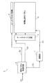
- FIG. 1 is a block diagram showing an example of the configuration of the organic EL display device according to the first embodiment.
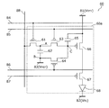
- FIG. 2 is a diagram illustrating an example of the configuration of the organic EL panel according to the first embodiment.
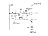
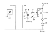
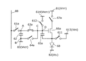
- FIG. 3 is a diagram illustrating an example of a circuit configuration of the display pixel according to the first embodiment.
- FIG. 4 is a diagram illustrating an example of the configuration of the adjustment unit according to the first embodiment.
- FIG. 5 is a diagram illustrating an example of a voltage adjustment method of the adjustment unit according to the first embodiment.
- FIG. 6 is a diagram showing a response time when the voltage of the adjustment unit according to the first embodiment is changed.
- FIG. 7 is a diagram illustrating a relationship between the adjustment unit and the pixel circuit according to the first embodiment.
- FIG. 1 is a block diagram showing an example of the configuration of the organic EL display device according to the first embodiment.
- FIG. 2 is a diagram illustrating an example of the configuration of the organic EL panel according to the first embodiment.
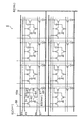
- FIG. 8 is a diagram illustrating a relationship between the pixel circuit and the power supply line according to the first embodiment.
- FIG. 9A is a diagram illustrating an example of the operation of the pixel circuit illustrated in FIG.
- FIG. 9B is a diagram illustrating an example of the operation of the pixel circuit illustrated in FIG. 3.
- FIG. 9C is a diagram illustrating an example of the operation of the pixel circuit illustrated in FIG. 3.
- FIG. 9D is a diagram illustrating an example of the operation of the pixel circuit illustrated in FIG. 3.
- FIG. 9E is a diagram illustrating an example of the operation of the pixel circuit illustrated in FIG. 3.
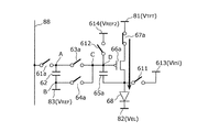
- FIG. 10 is a diagram illustrating an example of a circuit configuration of a display pixel according to the second embodiment.
- FIG. 11 is a diagram illustrating a relationship between the adjustment unit and the pixel circuit according to the second embodiment.
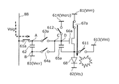
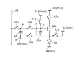
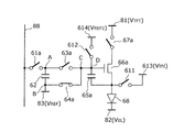
- 12A is a diagram illustrating an example of the operation of the pixel circuit illustrated in FIG. 12B is a diagram illustrating an example of the operation of the pixel circuit illustrated in FIG. 12C is a diagram illustrating an example of the operation of the pixel circuit illustrated in FIG. 12D is a diagram illustrating an example of the operation of the pixel circuit illustrated in FIG. 12E is a diagram illustrating an example of the operation of the pixel circuit illustrated in FIG.
- FIG. 12F is a diagram illustrating an example of operation of the pixel circuit illustrated in FIG. 10.
- FIG. 12G is a diagram illustrating an example of the operation of the pixel circuit illustrated in FIG.
- FIG. 12H is a diagram illustrating an example of operation of the pixel circuit illustrated in FIG.
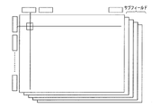
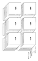
- FIG. 13 is a diagram conceptually illustrating a case where one frame according to Modification 1 is configured with a plurality of subfields.
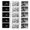
- FIG. 14 is a diagram illustrating an example of a frame including a plurality of subfields according to the first modification.
- FIG. 15 is a diagram illustrating an example of a frame including a plurality of subfields according to the second modification.
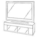
- FIG. 16 is an external view of a thin flat TV incorporating the organic EL display device of the present disclosure.
- One aspect of the organic EL display device includes a plurality of display pixels arranged in a matrix and an adjustment unit that adjusts a predetermined voltage applied to a power supply line connected to the plurality of display pixels.
- Each of the plurality of display pixels includes a light emitting element, a first capacitor element for holding a first voltage used for causing the light emitting element to emit light, and a first voltage held in the first capacitor element.
- a driving transistor that causes the light emitting element to emit light by supplying a current corresponding to the light emitting element, and a second voltage that is different from the first voltage held by the first capacitive element, and the first capacitive element is A second capacitance element for holding a voltage to be held, the power line is connected to a drain electrode of the driving transistor or a cathode of the light emitting element, and the adjustment unit is configured to display the plurality of display pixels.
- the voltage applied to the power supply line is adjusted to be lower than the predetermined voltage when the total value of the currents is equal to or greater than a threshold value. To do.
- the organic EL display device includes an adjustment unit, and can independently perform writing of a data signal voltage and display of an image.
- the overload restriction can be performed so that the panel power due to the current flowing into the organic EL panel does not exceed a certain level without deteriorating the video quality, it is possible to suppress a decrease in the lifetime of the organic EL element 68. it can.
- a control unit that controls each of the plurality of display pixels includes a first period in a light emission period in which the light emitting element emits light in each of the plurality of display pixels.
- the second capacitor element is held in the second capacitor element during a second period after an initialization period in which the first capacitor element is initialized in a non-light emission period after the light emission period.
- the second voltage held by the first capacitance element is copied to the first capacitance element so that the first capacitance element holds the first voltage, and the adjustment unit has a total current value corresponding to the second voltage equal to or greater than a threshold value.
- the voltage applied to the power supply line during the non-light emitting period may be adjusted to be lower than the predetermined voltage.
- the organic EL display device displays an image by dividing one frame period of a video signal into a plurality of subframe periods, and the light emitting element emits light, and the light emitting element emits light next.
- the period between the light emission periods may correspond to the subframe period.
- the adjustment unit when the current corresponding to the second voltage when the current corresponding to the second voltage is supplied to the light emitting elements in each of the plurality of display pixels, the adjustment unit is equal to or greater than a threshold value.
- the voltage applied to the power supply line may be adjusted by linearly changing over a predetermined time so as to be lower than the predetermined voltage.
- the driving transistor when the driving transistor is P-type, the driving transistor has a drain electrode connected to the first electrode of the first capacitor element and a gate electrode connected to the second electrode of the first capacitor element.
- the source electrode may be connected to the anode of the light emitting element, and the power line may be connected to the cathode of the light emitting element.
- each of the plurality of display pixels further includes a first switch that switches between conduction and non-conduction between a signal line for supplying a data signal voltage and the first electrode of the second capacitive element, and the first switch A second switch that switches between conduction and non-conduction between the first electrode of the two-capacitance element and the second electrode of the first capacitance element; a reference power supply line for supplying a reference voltage; and the first capacitance element A third switch that switches between conduction and non-conduction with the second electrode, and a fourth switch that switches between conduction and non-conduction between the source electrode of the drive transistor and the anode of the light emitting element, and the reference power supply line includes: It is also connected to the second electrode of the second capacitive element, and the first switch, the second switch, the third switch, and the fourth switch are P-type transistors. Good.
- the power supply line is connected to a drain electrode of the driving transistor, and the driving transistor has a source electrode connected to the first electrode of the first capacitor element and the light emitting element.
- the gate electrode may be connected to the second electrode of the first capacitor element.
- each of the plurality of display pixels further includes a first switch that switches between conduction and non-conduction between a signal line for supplying a data signal voltage and the first electrode of the second capacitive element, and the first switch A second switch that switches between conduction and non-conduction between the first electrode of the two-capacitance element and the second electrode of the first capacitance element; a reference power supply line for supplying a reference voltage; and the first capacitance element A third switch that switches between conduction and non-conduction with the second electrode; and a fourth switch that switches between conduction and non-conduction between the drain electrode of the driving transistor and the power supply line, and the reference power supply line includes the second switch
- the first switch, the second switch, the third switch, and the fourth switch may be N-type transistors, and are also connected to the second electrode of the capacitor.
- An aspect of the driving method according to the present invention is a driving method of an organic EL display device including a plurality of display pixels arranged in a matrix, and the organic EL display device includes a plurality of organic EL display devices arranged in a matrix. Display pixels and a power supply line connected to the plurality of display pixels to which a predetermined voltage is applied, each of the plurality of display pixels being used for emitting a light emitting element and the light emitting element.
- a second voltage element that is a second voltage different from the first voltage held by the one capacitor element and that holds the voltage that the first capacitor element should hold next, and the power supply line includes: Driving transistor Connected to the drain electrode or the cathode of the light emitting element, and the driving method is such that a total value of the currents when a current corresponding to the second voltage is supplied to the light emitting elements in each of the plurality of display pixels is greater than or equal to a threshold value In this case, the voltage applied to the power supply line is adjusted to be lower than the predetermined voltage, and the current corresponding to the second voltage held in the first capacitor element is supplied to the light emitting element in the driving transistor. Supply.
- FIG. 1 is a block diagram showing an example of the configuration of the organic EL display device according to the first embodiment.
- 1 includes a display panel control circuit 2, a gate driver IC (circuit) 3, a source driver IC (circuit) 5, an organic EL display panel 6, and an adjustment unit 7.
- EL elements composed of three primary colors of red (R), green (G), and blue (B) are formed in a matrix.
- a color filter composed of red (R), green (G), and blue (B) can be formed.
- the color filter is not limited to RGB, and may form pixels of cyan (C), magenta (M), and yellow (Y).
- white (W) pixels may be formed. That is, R, G, B, and W pixels are arranged in a matrix on the display screen.
- the pixel aperture ratios of R, G, and B may be different. By varying the aperture ratio, it is possible to vary the density of current flowing through each RGB light emitting element (organic EL element 68). By making the current densities different, the degradation rates of the RGB light emitting elements can be made the same. If the deterioration rates are the same, the white balance deviation of the organic EL display panel 6 does not occur.
- the pixel is composed of R, G, B, and W.
- R, G, B, and W high luminance can be achieved.
- configurations of R, G, B, and G are also exemplified.
- the colorization of the organic EL display panel 6 is performed by mask vapor deposition, but this embodiment is not limited to this.
- a blue light emitting EL layer may be formed, and the emitted blue light may be converted into R, G, B light by an R, G, B color conversion layer (CCM: Color Change Mediums).
- a circularly polarizing plate (circularly polarizing film) (not shown) can be disposed on the light exit surface of the organic EL display panel 6. What integrated the polarizing plate and the phase film is called a circularly polarizing plate (circularly polarizing film).
- the display panel control circuit 2 generates a control signal S2 for controlling the source driver IC (circuit) 5 based on the display data signal S1, and outputs the generated control signal S2 to the source driver IC (circuit) 5.
- the display panel control circuit 2 generates a control signal S3 for controlling the gate driver IC (circuit) 3 based on the synchronization signal included in the display data signal S1. Then, the display panel control circuit 2 outputs the generated control signal S3 to the gate driver IC (circuit) 3.
- the display data signal S1 is a signal indicating display data including a video signal, a vertical synchronization signal, and a horizontal synchronization signal.
- the video signal is a signal that designates each pixel value that is gradation information for each frame.
- the vertical synchronization signal is a signal for synchronizing the processing timing in the vertical direction with respect to the screen, and is a signal serving as a reference for processing timing for each frame.
- the horizontal synchronization signal is a signal for synchronizing the processing timing in the horizontal direction with respect to the screen.
- the control signal S2 includes a video signal and a horizontal synchronization signal.
- the control signal S3 includes a vertical synchronization signal and a horizontal synchronization signal.
- the gate driver IC (circuit) 3 drives the gate signal line of the organic EL display panel 6 based on the control signal S3 generated by the display panel control circuit 2.
- the source driver IC (circuit) 5 drives the source signal line of the organic EL display panel 6 based on the control signal S2 generated by the display panel control circuit 2. More specifically, the source driver IC (circuit) 5 outputs a source signal (data signal voltage) to each pixel circuit based on the video signal and the horizontal synchronization signal.
- the adjusting unit 7 adjusts a predetermined voltage applied to a power line (EL cathode power line) connected to a plurality of display pixels based on the display data signal S1 transmitted through the display panel control circuit 2. Since details will be described later, description thereof is omitted here.
- a power line EL cathode power line
- the organic EL display device 1 includes, for example, a CPU (Central Processing Unit), a storage medium such as a ROM (Read Only Memory) storing a control program, a working memory such as a RAM (Random Access Memory), although not illustrated. And a communication circuit.
- the display data signal S1 is generated, for example, when the CPU executes a control program.
- FIG. 2 is a diagram showing an example of the configuration of the organic EL display panel according to the first embodiment.
- FIG. 2 shows the positions and connection relationships of the organic EL display panel 6, the gate driver IC (circuit) 3, and the source driver IC (circuit) 5.
- the organic EL display panel 6 includes a gate signal line 84, a gate signal line 85, a gate signal line 85, a gate signal line 86, and a gate driver IC (circuit) 30 and a gate driver IC (circuit) 31.
- a gate signal line 87 is connected.
- the organic EL display panel 6 is connected to a source signal line 88 controlled by the source driver IC (circuit) 5.
- the gate signal line 84, the gate signal line 85, the gate signal line 86, the gate signal line 87, and the source signal line 88 will be described later.
- the gate driver IC (circuit) 3 includes a gate driver IC (circuit) 30 and a gate driver IC (circuit) 31, and gate driver ICs (circuits) are arranged on the left and right sides of the organic EL display panel 6. ) 30 and the gate driver IC (circuit) 31 are configured, but this configuration is an example. Only one of the left and right gate driver ICs (circuits) 3 may be provided.
- 5 is described as a source driver IC, but is not limited to a source driver IC made of a semiconductor chip.
- a source driver IC made of a semiconductor chip.
- a transistor formed of a silicon wafer, peeled off and transferred to a glass substrate is exemplified.
- a display panel in which a transistor chip is formed using a silicon wafer and a glass substrate is mounted by bonding is exemplified.
- a source driver circuit may be formed directly on a glass substrate on which pixels are formed using low-temperature polysilicon, high-temperature polysilicon, TAOS technology, or the like.
- 30 and 31 are described as gate driver ICs, they are not limited to source driver ICs made of semiconductor chips.
- a transistor formed of a silicon wafer, peeled off and transferred to a glass substrate is exemplified.
- a display panel in which a transistor chip is formed using a silicon wafer and a glass substrate is mounted by bonding is exemplified.
- a source driver circuit may be formed directly on a glass substrate on which pixels are formed using low-temperature polysilicon, high-temperature polysilicon, TAOS technology, or the like.
- FIG. 3 is a diagram illustrating an example of a circuit configuration of the display pixel according to the first embodiment.
- the display pixel according to the first embodiment includes a transistor, a capacitor, an EL element, and the like.
- the transistor including the driving transistor and the switching transistor is described as a thin film transistor (TFT), but is not limited thereto.
- TFT thin film transistor
- An FET, a MOS-FET, a MOS transistor, or a bipolar transistor may be used. These are also basically thin film transistors.
- varistors, thyristors, ring diodes, photodiodes, phototransistors, PLZT elements may be used.
- the transistor is not limited to a thin film element, and may be a transistor formed on a silicon wafer.
- a transistor formed of a silicon wafer, peeled off and transferred to a glass substrate is exemplified.
- a display panel in which a transistor chip is formed using a silicon wafer and a glass substrate is mounted by bonding is exemplified.
- the transistor adopts an LDD (Lightly Doped Drain) structure for both n-type and p-type transistors.
- LDD Lightly Doped Drain
- Transistors include high-temperature polysilicon (HTPS: high-temperature polycrystalline silicon), low-temperature polysilicon (LTPS: low-temperature polysilicon), continuous grain boundary silicon (CGS: continuous grain silicon), and transparent amorphous oxide semiconductor (TAOS: Any one of transparent (Amorphous) Oxide (Semiconductors, IZO), amorphous silicon (AS: Amorphous Silicon), and infrared RTA (RTA: Rapid Thermal Annealing) may be used.
- HTPS high-temperature polycrystalline silicon
- LTPS low-temperature polysilicon
- CGS continuous grain silicon
- TAOS transparent amorphous oxide semiconductor
- IZO transparent (Amorphous) Oxide
- AS amorphous silicon
- RTA Rapid Thermal Annealing
- all the transistors constituting the display pixel are p-type.
- the present disclosure is not limited to only configuring the pixel transistor to be p-type. You may comprise only n-type. Moreover, you may comprise using both n-type and p-type.
- the switch transistor is not limited to a transistor, and may be, for example, an analog switch configured using both a p-type transistor and an n-type transistor.
- the transistor preferably has a top gate structure.
- the parasitic capacitance is reduced, the gate electrode pattern of the top gate becomes a light shielding layer, and the light emitted from the EL element is blocked by the light shielding layer, so that malfunction of the transistor and off-leakage current can be reduced. is there.
- the gate signal line driven (controlled) by the gate driver IC (circuit) has a low impedance. Therefore, the same applies to the configuration or structure of the gate signal line.
- the transistor has a top gate structure and a small parasitic capacitance, so that n-type and p-type transistors can be manufactured, and a copper wiring or copper alloy wiring process can be used for the process.
- the copper wiring preferably employs a three-layer structure of Ti—Cu—Ti.
- the wiring such as the gate signal line or the source signal line preferably employs a three-layer structure of molybdenum (Mo) -Cu-Mo. .
- the capacitor is formed or arranged so as to overlap (overlap) at least one of the source signal line and the gate signal line.
- the degree of freedom in layout is improved, a wider space between elements can be secured, and the yield is improved.
- An insulating film or an insulating film (planarizing film) made of an acrylic material is formed on the source signal line and the gate signal line for insulation, and a pixel electrode is formed on the insulating film.
- a pixel circuit 60 shown in FIG. 3 is one pixel of the organic EL display panel 6 and has a function of emitting light by a source signal (video signal voltage) supplied via a source signal line 88.
- the pixel circuit 60 is an example of a display pixel (light emitting pixel), and is arranged in a matrix (matrix).
- the pixel circuit 60 includes a switch 61, a capacitive element 62, a switch 63, a switch 64, a capacitive element 65, a driving transistor 66, a switch 67, and an organic EL element 68.
- the pixel circuit 60 includes an EL anode power line 81 (V TFT ), an EL cathode power line 82 (V EL ), a reference power line 83 (V REF ), a gate signal line 84, a gate signal line 85, and a gate signal line 86.
- the source signal line 88 is an example of a signal line (source signal line) for supplying a data signal voltage (source signal).
- the EL anode power line 81 (V TFT ) is connected to the drain electrode of the driving transistor and is a high voltage side power line for determining the potential of the drain electrode of the driving transistor 66, and is 6 (v), for example.
- the EL cathode power line 82 (V EL ) is a low voltage side power line connected to the cathode (second electrode) of the organic EL element 68.
- the reference power supply line 83 (V REF ) is an example of a power supply line for supplying a reference voltage, and supplies the reference voltage V REF .
- the potential difference between the reference power source line 83 (V REF) reference voltage V REF and the EL anode power supply line 81 (V TFT) supplied by the anode voltage V TFT supplies is than the threshold voltage of the driving transistor 66 (Vth)
- Vth A large voltage, that is, a threshold voltage Vth ⁇ (anode voltage V TFT ⁇ reference voltage V REF ) is set.
- the reference voltage V REF is, for example, 0V.
- the organic EL element 68 is an example of a light emitting element that emits light according to the current supplied by the driving transistor 66, and is arranged in a matrix.
- the organic EL element 68 has a cathode (second electrode) connected to the EL cathode power supply line 82 and an anode (first electrode) connected to the source (source electrode) of the drive transistor 66 via the switch 67.
- the voltage supplied to the EL cathode power supply line 82 is V EL, for example -6 (v).
- the drive transistor 66 is a voltage-driven drive element that controls the supply of current to the organic EL element 68, and supplies the organic EL element 68 with a current corresponding to the voltage held in the capacitive element 65. 68 emits light. More specifically, as shown in FIG. 3, in the driving transistor 66, the drain electrode is electrically connected to the first electrode of the capacitor 65, the gate electrode is electrically connected to the second electrode of the capacitor 65, and the source electrode is organic. The anode of the EL element 68 is connected via the switch 67.
- the drive transistor 66 causes the organic EL element 68 to emit light by causing a current corresponding to the voltage (data signal voltage) held in the display capacitive element 65 to flow through the organic EL element 68 during the light emission period. More specifically, the drive transistor 66 converts the data signal voltage supplied to the gate electrode into a current corresponding to the data signal voltage, and supplies the converted current to the organic EL element 68, thereby providing an organic signal.
- the EL element 68 is caused to emit light. This light emission timing is controlled by the switch 67. In this embodiment, in all the pixel circuits 60 (all the pixels included in the organic EL display panel 6), the switches 67 are collectively controlled to be in an on state (conductive state). The organic EL elements 68 of all the pixels are turned on collectively. That is, the light emission period starts simultaneously on all screens.
- the drive transistor 66 does not flow current to the organic EL element 68 by controlling the switch 67 to be in an off state (non-conduction state). That is, the drive transistor 66 does not cause the organic EL element 68 to emit light during the non-light emission period.
- the thin film transistor (TFT) included in the driving transistor 66 is assumed to be P-type.
- the thin film transistor (TFT) constituting the driving transistor 66 may be N-type, P-type, or a combination of both.
- the channel layer of the thin film transistor may be formed of any one of amorphous silicon, microcrystalline silicon, polysilicon, an oxide semiconductor, an organic semiconductor, and the like.
- an oxide semiconductor material containing at least one of indium (in), gallium (Ga), and zinc (Zn) can be used for the oxide semiconductor.
- An oxide semiconductor has low off-state current, high electron mobility even in an amorphous state, and can be formed by a low-temperature process.
- an oxide semiconductor can be formed using amorphous indium gallium zinc oxide (InGaZnO).
- the capacitive element 65 is an example of a first capacitive element (display capacitor) for holding a first voltage used for causing the organic EL element 68 to emit light.
- the capacitive element 65 holds a voltage that determines the amount of current that the driving transistor 66 flows.
- the first electrode (electrode opposite to the node C side) of the capacitive element 65 is between the drain electrode (electrode on the EL anode power supply line 81 side) of the drive transistor 66 and the EL anode power supply line 81. It is connected.
- a second electrode (electrode on the node C side) of the capacitive element 65 is connected to the gate electrode of the driving transistor 66.
- the second electrode of the capacitive element 65 is connected to the first electrode (electrode on the node A side) of the capacitive element 62 via the switch 63.
- a second electrode of the capacitive element 65 is connected to a reference power supply line 83 (V REF ) that supplies a reference voltage V REF via a switch 64.
- the capacitive element 65 is controlled by the display panel control circuit 2 in the non-light emitting period after the light emitting period in which the organic EL element 68 emits light, after the initialization period in which the capacitive element 65 is initialized.
- the second voltage held by the capacitor 62 is copied and held as the first voltage.
- the capacitive element 62 is an example of a second capacitive element (write capacitor) that is a second voltage different from the first voltage held by the capacitive element 65 and that holds the voltage that the capacitive element 65 should hold next. .
- the capacitor 62 serves as a memory that temporarily holds a voltage that the capacitor 65 should hold next.
- the first electrode (node A side electrode) of the capacitive element 62 is connected to the source signal line 88 through the switch 61.
- the second electrode (electrode on the node B side) of the capacitive element 62 is also connected to a reference power supply line 83 (V REF ) that supplies a reference voltage V REF .
- the capacitor 62 holds the second voltage by writing the second voltage in the first period during the light emission period in which the organic EL element 68 emits light under the control of the display panel control circuit 2. .
- the switch 61 is an example of a first switch that switches between conduction and non-conduction between the source signal line 88 (signal line) for supplying the data signal voltage and the first electrode of the capacitive element 62. Specifically, in the switch 61, one terminal of the drain and the source is connected to the source signal line 88, the other terminal of the drain and the source is connected to the first electrode of the capacitor 62, and the gate is the gate signal line 84. Is a switching transistor connected to. In other words, the switch 61 writes the data signal voltage (data signal) corresponding to the video signal voltage (video signal) supplied via the source signal line 88 to the capacitive element 62 (write capacitor) that temporarily holds the data signal voltage. Has a function for.
- the switch 63 is an example of a second switch that switches between conduction and non-conduction between the first electrode of the capacitive element 62 and the second electrode of the capacitive element 65. Specifically, in the switch 63, one terminal of the drain and the source is connected to the first electrode of the capacitor 62, and the other terminal of the drain and the source of the switch 63 is connected to the second electrode of the capacitor 65, This is a switching transistor whose gate is connected to the gate signal line 85. In other words, the switch 63 has a function of applying (copying) the second voltage held by the capacitor 62 to the capacitor 65.
- the switch 64 is an example of a third switch that switches between conduction and non-conduction between the reference power supply line 83 (V REF ) that supplies the reference voltage V REF and the second electrode of the capacitive element 65.
- V REF reference power supply line 83
- the other terminal of the drain and the source is the gate electrode of the driving transistor 66 and the second element of the capacitor 65.
- the switching transistor is connected to the electrode and the gate is connected to the gate signal line 86.
- the switch 64 has a function of supplying the reference voltage (V REF ) to the second electrode of the capacitor 65 and the gate electrode of the driving transistor 66.
- the switch 67 is an example of a fourth switch that switches between conduction and non-conduction between the source electrode of the drive transistor 66 and the anode of the organic EL element 68.
- the switch 67 has one of drain and source terminals connected to the source electrode of the drive transistor 66, the other drain and source terminal connected to the anode of the organic EL element 68, and a gate connected to the gate signal line.
- 86 is a switching transistor connected to 86.
- the video signal voltage can be written to the pixel even when a current is supplied to the organic EL element 68.
- a voltage corresponding to the video signal written to the pixel in the previous frame period is held by a capacitor (capacitor element 65), and the drive transistor 66 is based on the voltage held by the capacitor element 65. To supply current.
- pixel rows are sequentially selected by a gate driver IC (circuit), and the source driver IC applies a video signal to the selected pixel (display pixel).
- a voltage corresponding to the video signal is held in the capacitive element 62.
- the voltage held in the capacitive element 62 is copied to the capacitive element 65. During this period, the display screen is maintained in a non-display state.
- the driving transistor 66 supplies current to the organic EL element 68 based on the voltage held in the capacitive element 65.
- the pixel in this embodiment includes the capacitor 65 and the capacitor 62 that hold a voltage based on a video signal.
- the capacitive element 65 and the capacitive element 62 that hold the voltage based on the video signal are provided.
- the present invention is not limited to this.
- two memory circuits may be constituted by transistors or the like, and the memory circuit may hold a voltage based on the video signal. Further, the voltage based on the video signal may be held in the gate capacitance of the MOS transistor.
- the switch 61, the switch 63, the switch 64, and the switch 67 that constitute the pixel circuit 60 are described as P-type TFTs, but the present invention is not limited thereto, and may be N-type TFTs.
- FIG. 4 is a diagram illustrating an example of the configuration of the adjustment unit according to the first embodiment.
- the adjustment unit 7 includes a current calculation unit 71, a voltage calculation unit 72, and a voltage change unit 73, and a predetermined voltage (cathode voltage V EL ) applied to the EL cathode power supply line 82 connected to the plurality of display pixels. Adjust.
- the current calculation unit 71 calculates a current value flowing through the organic EL display panel 6 when a data signal voltage based on display data (video data) included in the display data signal S1 is supplied to the organic EL display panel 6.
- the current calculation unit 71 includes a first current value calculation unit 711, a second current value calculation unit 712, a third current value calculation unit 713, a weighting unit 714, a weighting unit 715, and a weighting unit 716. , And an adder 717.
- the first current value calculation unit 711 is an organic EL display panel. 6 calculates a current value (first current value) flowing through the circuit 6.
- the second current value calculation unit 712 and the third current value calculation unit 713 are configured to display the green data signal voltage and the green data of the green data (Gdata) and the blue data (Bdata) included in the display data (video data).
- the weighting unit 714 weights the first current value calculated by the first current value calculation unit 711 and outputs it to the addition unit 717. This is because the color light emission efficiency of the organic EL element 68 varies depending on the material and the like. In the present embodiment, the weighting unit 714 weights, for example, 2, that is, doubles the first current value, and outputs the result to the adding unit 717. Similarly, the weighting unit 715 weights the second current value calculated by the second current value calculation unit 712 and outputs it to the addition unit 717, and the weighting unit 716 calculates the first current value calculated by the third current value calculation unit 713. The three current values are weighted and output to the adder 717. In the present embodiment, the weighting unit 715 weights 1 for example, and the weighting unit 716 weights 5 for example.
- the addition unit 717 outputs the total current value obtained by adding the weighting unit 714, the weighting unit 715, and the weighting unit 716 (taking the sum) to the voltage calculation unit 72.
- the total current value is a current value that flows through the organic EL display panel 6 when a data signal voltage based on the display data included in the display data signal S ⁇ b> 1 is supplied to the organic EL display panel 6.
- the voltage calculation unit 72 is described as obtaining the total current value in order to facilitate understanding, but is not limited thereto. Any value, size, amount of change, etc. may be used as long as the current or power flowing through the display screen of the organic EL display panel 6 has a proportional or predetermined correlation.
- a value correlated with the current value is obtained by calculating display data (video data), and the value correlated with the current value and the cathode voltage V EL , A value correlated with the power value can be obtained by multiplying with the anode voltage V TFT or the like.
- the cathode voltage V EL , the anode voltage V TFT, etc. are changed by the voltage changing unit 73 or the like, the cathode voltage V EL , the anode voltage V TFT is multiplied and the value corresponding to the power can be obtained. .
- the present invention is not limited to calculating the current by calculating all display data (video data) constituting the display screen.
- the current may be obtained by calculating display data (video data) corresponding to an arbitrary pixel selected on the display screen.
- the total current flowing in the display screen can be estimated by multiplying proportionally from any selected pixel. In this case, the calculation time for calculating the current value and the number of calculations can be reduced.
- the current may be obtained by calculating display data (video data) having a higher gradation than a predetermined level. Further, a value corresponding to the current may be obtained from the number of pixels of display data (video data) having a higher gradation than a predetermined level. Based on the total current value output from the adder 717, the voltage calculation unit 72 determines whether to change from a predetermined voltage applied by the EL cathode power supply line 82, and if so, applies the EL cathode power supply line 82. The power voltage is calculated.
- the voltage calculation unit 72 determines that the predetermined voltage applied to the EL cathode power supply line 82 should be changed when the total current value output by the addition unit 717 is equal to or greater than a predetermined threshold value. A voltage higher than the predetermined voltage is calculated as a voltage to be applied to the EL cathode power supply line 82.
- the voltage changing unit 73 changes the voltage (cathode voltage) so that the voltage value calculated by the voltage calculating unit 72 is obtained. For example, when the current flowing through the organic EL display panel 6 is in a predetermined value range (in the case of a steady range), the voltage of the EL cathode power supply line 82 is ⁇ 6 (v), and the current flowing through the EL display panel is When the voltage exceeds the predetermined value, the voltage of the EL cathode power supply line 82 is set to ⁇ 4 (v).
- FIG. 5 is a diagram illustrating an example of a voltage adjustment method of the adjustment unit according to the first embodiment.
- the horizontal axis represents the lighting rate (%).
- the lighting rate is obtained by adding gradation data such as a video signal.
- the lighting rate has a maximum value of 100% and a minimum value of 0%. However, it is necessary to obtain the lighting rate by weighting with the light emission efficiency of each color light emitting element such as red (R), green (G), and blue (B).
- the organic EL display panel 6 since the luminous efficiency is different for each of the red (R), green (G), and blue (B) EL elements, a weighting coefficient is assigned to the gradation data according to R, G, and B. Then, the addition data of the display screen is obtained. In the case of R, G, B, and W (white), the four colors are weighted based on the light emission efficiency.
- the gradation data is gamma-converted, the gradation data is calculated with a gamma conversion coefficient, and the current flowing through the organic EL element is obtained.
- a weighting process is performed on the obtained current based on the light emission efficiency of each emission color. For example, if the weighting coefficient of green (G) is 1 and the luminous efficiency of red (R) is 1/2 that of green (G), the weighting coefficient of red (R) is 2. Further, if the luminous efficiency of blue (B) is 1/5 of that of green (G), the weighting coefficient of blue (B) is 5.
- the lighting rate of 0% means that the display screen is black and the previous pixel is not lit. Therefore, ideally, no current flows through the organic EL element on the display screen.
- a lighting rate of 100% is white display with the highest luminance (maximum brightness) on the display screen. That is, all the pixels on the display screen are displaying with the maximum gradation, and the current flowing through the display screen is the maximum value.
- the lighting rate can be calculated by multiplying the current flowing through the EL element of each emission color by the weighting coefficient. It can.
- the lighting rate is obtained by weighting the current flowing through the display screen based on the light emission efficiency of the light emission colors arranged in a matrix.
- the lighting rate (%) It can be expressed as Ix / Im ⁇ 100.
- the cathode voltage and anode voltage are set to constant values (fixed values).
- the current flowing through the display screen (or a value correlated with the current) is acquired from the gradation data.
- each RGB current flowing through the cathode wiring or anode wiring may be measured with an ammeter or the like and weighted with each RGB current.
- the current flowing through the display screen may be measured, and the lighting rate may be obtained from the measured current.
- a current value flowing through the display screen may be obtained by arranging a pickup resistor in series between the EL cathode power supply line 82 and the EL anode power supply line 81 and measuring the voltage across the pickup resistance with a voltmeter. .
- the current data obtained by obtaining gradation data, or the current obtained by directly measuring the current can be obtained as current consumption (power consumption) flowing through the display screen if the anode voltage and cathode voltage are fixed values. it can.
- the current consumption is correlated with the value obtained by weighting the image signal such as RGB based on the efficiency of the EL element.
- the lighting rate is determined from the gradation data of the entire display screen or the flowing current, but is not limited to this. From the added value or current of gradation data in a part of the display screen (for example, 1/4 of the display screen), the added value or current of the gradation data of all display screens is estimated or obtained, and the lighting rate is obtained. Also good. Further, the lighting rate is not limited to being obtained from the addition value or current of gradation data in one frame period. For example, it goes without saying that the lighting rate may be obtained by averaging or moving and integrating the addition value or current of gradation data in a plurality of frames.
- the cathode voltage is ⁇ 7 (V) as a constant value in the lines of all examples.
- the lighting rate is as low as 25% or less, even if the cathode voltage is low (the absolute value of the anode-cathode voltage is large), the current flowing through the display screen is small and the panel heat generation is small. There is no.
- the lighting rate is high, the current flowing through the display screen becomes large, so the cathode voltage is increased.
- the adjustment unit 7 has a total current value (or lighting rate) corresponding to the second voltage that is equal to or greater than the threshold when the current corresponding to the second voltage is supplied to the organic EL element 68 in each of the plurality of display pixels.
- the voltage applied to the EL cathode power supply line 82 is adjusted by changing the voltage so as to be higher than a predetermined voltage (voltage V EL ) (so that the potential difference between the anode voltage and the cathode voltage is reduced). More specifically, the voltage changing unit 73 does not make the change in the cathode voltage steep, but changes the voltage so as to follow a straight line L1 having a certain gradient as shown in FIG. 5, for example.
- the voltage adjustment method is not limited to changing the cathode voltage along the straight line L1, but may be changed along the straight line L2 having a gentler slope than the straight line L1. Further, as shown by a line L3, the voltage may be adjusted from a constant lighting rate of 25%, and the lighting rate of 65% or more may be changed to maintain a constant voltage.
- FIG. 6 is a diagram showing the response time when the voltage of the adjustment unit according to the first embodiment is changed.
- the vertical axis in FIG. 6 indicates the response time (msec order), and the horizontal axis indicates the amount of change in the total current value (or lighting rate). That is, the voltage changing unit 73 is not limited to the case where the cathode voltage is changed sharply at the inflection point so as to be along the straight line L5, and may be changed smoothly along the curve L6.
- the adjustment unit 7 includes the current corresponding to the second voltage or the total value of the gradation values (lighting rate) when the current corresponding to the second voltage is supplied to the organic EL element 68 in each of the plurality of display pixels. ) Is equal to or greater than the threshold value, the voltage applied to the EL cathode power supply line 82 is adjusted to be lower than a predetermined voltage.
- the adjustment unit 7 uses the EL cathode power supply line 82 during the non-light emitting period of the pixel circuit 60 when the total value (lighting rate) of the current or gradation value corresponding to the second voltage is equal to or greater than the threshold value.
- the voltage applied to is adjusted to be lower than a predetermined voltage. Since the details of the adjustment timing will be described later, a description thereof is omitted here.
- the adjustment part 7 can perform an overload restriction
- FIG. This is because a current corresponding to the applied voltage (gradation signal voltage) flows through the organic EL element 68 by the driving transistor 66. And if the electric current which flows into the display pixel (organic EL element 68) which comprises the organic EL display panel 6 is large, the organic EL display panel 6 will generate
- FIG. 7 is a diagram illustrating a relationship between the adjustment unit and the pixel circuit according to the first embodiment. 3 and 4 are denoted by the same reference numerals, and detailed description thereof is omitted.
- Adjuster 7 (voltage changing unit 73), so that the voltage value calculated by the voltage calculation unit 72, changes the voltage V EL of the EL cathode power supply line 82 of the pixel circuits 60a (voltage V EL of the voltage source 73a) To do.
- FIG. 8 is a diagram showing a relationship between the pixel circuit and the power supply line according to the first embodiment.
- the pixel circuits 60a are arranged in a matrix (matrix) in the organic EL display panel 6, as shown in FIG. As shown in FIG. 6, the EL anode power line 81 and the EL cathode power line 82 are provided as a common power line for the plurality of pixel circuits 60a, not for each of the pixel circuits 60a.
- the writing process of the luminance signal and the light emitting process of the organic EL element can be performed independently.
- the display pixel of the present embodiment that is, the pixel circuit 60 shown in FIG. 3 is driven by executing a writing process, a reset process, a copy process, a voltage adjustment process, and a light emission process.
- the driving method according to the present embodiment can be realized by performing the five processes shown in FIGS. 9A to 9E with the configuration of the pixel circuit 60 shown in FIG.
- 9A to 9E are diagrams illustrating an example of the operation of the pixel circuit according to the first embodiment.
- 9A to 9E show scene operations corresponding to the writing process, the reset process, the copy process, the voltage adjustment process, and the light emission process, respectively. Elements similar to those in FIG. 3 are denoted by the same reference numerals, and detailed description thereof is omitted.
- FIG. 9A shows an operation scene of the writing process, which is executed in the first period during the light emission period in which the organic EL element 68 emits light. That is, as shown in FIG. 9A, the writing process is performed on the capacitor 62 in the first period during the light emission period in which the organic EL element 68 emits light according to the current video signal voltage of the capacitor 65. This is processing in which the video signal voltage (Vsig) for the light emission period is written.
- Vsig video signal voltage
- the switch 63 and the switch 64 are kept in a non-conduction state (off state), and the switch 67 is kept in a conduction state (on state), and is held in the drive transistor 66 and the capacitor 65.
- a current corresponding to the voltage is supplied to the organic EL element 68 and the organic EL element 68 emits light (light emission period).
- the switch 61 is turned on (on state), whereby the voltage that the capacitor 65 should hold next in the capacitor 62 (video signal voltage Vsig). Hold.
- the second voltage (voltage) is applied to the capacitor 62 during the light emission period (during the first period) in which the organic EL element 68 emits light in each of the plurality of pixel circuits 60 by the display panel control circuit 2.
- Next video signal voltage is written and held.
- the above operations are sequentially performed from the uppermost pixel row to the lowermost pixel row of the screen. That is, the gate driver circuit 3 performs a shift operation, and performs an operation of sequentially selecting pixel row positions to which video signals are applied.
- the next light emission is performed in the first period during the light emission period in which the voltage (video signal voltage) held in the capacitor element 65 is caused to emit light to the organic EL element 68.
- a voltage (video signal voltage) that should be held in the capacitor 65 during the period can be written and held in the capacitor 62 in advance. That is, according to the pixel circuit 60 according to the present embodiment, the next video signal voltage (video data) can be written into the pixel circuit 60 even when the organic EL element 68 is emitting light. Therefore, the next image display can be written in each pixel while maintaining the image display state of the display screen.
- FIG. 9B shows an operation scene of the reset process, which is executed during a non-light emission period after the organic EL element 68 emits light.
- the non-light emitting period is exemplified by a blanking period. That is, as illustrated in FIG. 9B, the reset process is a process in which the capacitor element 65 is reset in a state where the light emission of the organic EL element 68 is stopped.
- the switch 64 and the switch 63 are kept in the non-conduction state (off state) while the switch 67 is in the non-conduction state (off state), while the switch 64 is in the conduction state (on state). State), the voltage V REF is input to one end of the capacitor 65. Thereby, the reset process in which the capacitive element 65 is initialized is executed.
- FIG. 9C shows an operation scene of the copy process, and is executed in the second period after the reset process in the non-emission period in which the light emission of the organic EL element 68 is stopped. That is, as shown in FIG. 9C, in the copy process, the next video signal voltage (Vsig) held by the capacitor 62 is copied to the capacitor 65 in the second period after the reset process in the non-light emission period. It is processing.
- Vsig video signal voltage
- the switch 63 is maintained in the non-conduction state (off state) during the second period after the reset process is performed during the non-light emission period in which the switch 67 is in the non-conduction state (off state).
- the switch 63 is turned on (on state).
- the first electrode of the capacitive element 62 and the second electrode of the capacitive element 65 are connected, and the next video signal voltage (Vsig) held in the capacitive element 62 is copied (written) to the capacitive element 65.
- Vsig video signal voltage
- the video signal voltage held in the capacitive element 62 of each pixel is copied to the capacitive element 65 all at once.
- an image is displayed with the video signal voltage copied to the capacitive element 65.
- FIG. 9D shows an operation scene of voltage adjustment processing in which a predetermined voltage (cathode voltage) is adjusted by the adjustment unit 7, and is executed in a non-light emission period in which the light emission of the organic EL element 68 is stopped. That is, as shown in FIG. 9D, the voltage adjustment process is a process of adjusting the cathode voltage of the EL cathode power supply line 82 (the voltage V EL of the voltage source 73a) during the non-emission period.
- a predetermined voltage cathode voltage
- FIG. 9D shows a scene in which the voltage adjustment process is executed in parallel with the copy process shown in FIG. 9C, but is not limited thereto.
- the switch 67 may be in a non-light emitting period in which the switch 67 is in a non-conduction state (off state).
- the reset process, copy process, and voltage adjustment process are performed during the blanking period as an example. During these operation periods, the shift operation of the gate driver circuit is stopped. Further, these operations are performed simultaneously on all the pixels of the display screen.
- the adjustment unit 7 obtains the current flowing through the organic EL display panel 6 by calculation from the display data signal S1 of the subfield or one frame, and changes the anode voltage from the result so as to be lower than the predetermined voltage ( adjust. As a result, overload limitation can be performed so that the panel power due to the current flowing into the organic EL display panel 6 does not exceed a certain level. Further, the adjustment unit 7 is combined with the pixel circuit 60 of the present embodiment to change the anode voltage which is an overload limit without degrading the image quality during the non-light emission period before the image is displayed. be able to.
- FIG. 9E shows an operation scene of the light emission processing, and the organic EL element 68 emits light.
- the switch 67 is turned on (on state) while the switch 61, the switch 63, and the switch 64 are maintained in a non-conductive state (off state).
- the organic EL element 68 can emit light according to the next video signal voltage (Vsig) held in the capacitive element 65.
- an image (for example, a moving image) can be displayed on the plurality of display pixels of this embodiment. it can.
- all the display pixels configured in the organic EL display panel 6 are switched from the non-conductive state (off state) to the conductive state (on state) at the same time, thereby switching all the frame displays.
- the display pixels can be executed simultaneously. That is, the display based on the current video signal voltage and the display based on the next video signal voltage can be displayed without being mixed.
- the organic EL display device 1 includes the adjusting unit 7 and can independently perform writing of the data signal voltage and display of the video. Further, the adjustment unit 7 changes the cathode voltage and the like to the blanking period.
- the video signals are sequentially copied to the capacitive element 62, but the video signals held in the capacitive element 62 are simultaneously copied to the capacitive element 65 during the blanking period.
- it is possible to limit overloading so that the panel power due to the current flowing into the organic EL panel does not exceed a certain level without degrading the video quality and without occurrence of flicker when changing the cathode voltage or the like.
- the lifetime reduction of the organic EL element 68 can be suppressed.
- the adjustment unit 7 obtains the current flowing through the organic EL display panel 6 from the subfield or the display data signal S1 of one frame by calculation, and changes the anode voltage from the result to be lower than the predetermined voltage. .
- overload limitation can be performed so that the panel power due to the current flowing into the organic EL display panel 6 does not exceed a certain level.
- the adjustment unit 7 can change the anode voltage, which is an overload limit, during the non-light emission period before the display of the video, there is an effect that the video quality is not deteriorated.
- the organic EL display device 1 of the present embodiment since overload restriction can be performed, a heat dissipation mechanism is not required for cooling the organic EL display panel 6, and the organic EL display panel 6 is thin. There is also an effect that can be realized.
- the switch 61, the switch 63, the switch 64, the driving transistor 66, and the thin film transistor that configures the switch 67 are described as being P-type.
- the case where the thin film transistors included in the switch 61, the switch 63, the switch 64, the driving transistor 66, and the switch 67 are N-type will be described. The following description will focus on the differences from the first embodiment.
- FIG. 10 is a diagram illustrating an example of a circuit configuration of the display pixel according to the second embodiment. Elements similar to those in FIG. 3 are denoted by the same reference numerals, and detailed description thereof is omitted.
- a pixel circuit 60A shown in FIG. 10 is one pixel of the organic EL display panel 6 and has a function of emitting light by a source signal (data signal voltage) supplied via a source signal line 88.
- the pixel circuit 60A is an example of a display pixel (light emitting pixel), and is arranged in a matrix (matrix).
- the pixel circuit 60A includes a switch 61a, a capacitive element 62, a switch 63a, a switch 64a, a capacitive element 65a, a drive transistor 66a, a switch 67a, an organic EL element 68, A switch 611 and a switch 612 are provided.
- the pixel circuit 60 includes an EL anode power line 81 (V TFT ), an EL cathode power line 82 (V EL ), a reference power line 83 (V REF ), a gate signal line 84 a, a gate signal line 85 a, and a gate signal line 86 a.
- an initialization power supply line 613 (V INI ), a reference power supply line 614 (V REF2 ), a control line 616, and an Init line 617 are further provided. .
- the initialization power supply line 613 is a power supply line that supplies a voltage V INI (also referred to as an initialization voltage V INI ) for initializing a voltage between the source and gate of the driving transistor 66 a, that is, a voltage of the capacitor 65. It is an example.
- the reference power line 614 (V REF2 ) is an example of a power line for supplying the reference voltage V REF2 .
- the organic EL element 68 is an example of a light emitting element that emits light according to the current supplied by the driving transistor 66a, and is arranged in a matrix.
- the drive transistor 66a is a voltage-driven drive element that controls the supply of current to the organic EL element 68, and supplies the organic EL element 68 with a current corresponding to the voltage held in the capacitive element 65a. 68 emits light.
- the thin film transistor (TFT) included in the driving transistor 66a is N-type.
- the capacitive element 65a is an example of a first capacitive element (display capacitor) for holding a first voltage used for causing the organic EL element 68 to emit light.
- the capacitive element 65a holds a voltage that determines the amount of current that the drive transistor 66a flows.
- the first electrode (electrode opposite to the node D side) of the capacitive element 65 a is connected between the source electrode (EL cathode power supply line 82 side) of the drive transistor 66 a and the anode of the organic EL element 68.
- the second electrode (electrode on the node D side) of the capacitive element 65a is connected to the gate electrode of the drive transistor 66a.
- the second electrode of the capacitor 65 a is also connected to the initialization power supply line 613 (V INI ) via the switch 611.
- the capacitive element 65a is controlled by the display panel control circuit 2 in the non-light emitting period after the light emitting period in which the organic EL element 68 emits light, after the initialization period in which the capacitive element 65a is initialized.
- the second voltage held by the capacitor 62 is copied and held as the first voltage.
- the capacitive element 62 is an example of a second capacitive element (write capacitor) that is a second voltage different from the first voltage held by the capacitive element 65a and that holds the voltage that the capacitive element 65a should hold next. .
- the capacitor 62 serves as a memory that temporarily holds a voltage that the capacitor 65a should hold next.
- the first electrode (electrode on the node A side) of the capacitive element 62 is connected to the source signal line 88 via the switch 61a.
- the second electrode (electrode on the node B side) of the capacitive element 62 is also connected to a reference power supply line 83 (V REF ) that supplies a reference voltage V REF .
- the capacitor 62 holds the second voltage by writing the second voltage in the first period during the light emission period in which the organic EL element 68 emits light under the control of the display panel control circuit 2. .
- the switch 61a is an example of a first switch that switches between conduction and non-conduction between the source signal line 88 (signal line) for supplying the data signal voltage and the first electrode of the capacitive element 62.
- the switch 63a is an example of a second switch that switches between conduction and non-conduction between the first electrode of the capacitive element 62 and the second electrode of the capacitive element 65a.
- the switch 64a is an example of a third switch that switches between conduction and non-conduction between the reference power supply line 83 (V REF ) that supplies the reference voltage V REF and the second electrode of the capacitive element 65a.
- the switch 67a is an example of a fourth switch that switches between conduction and non-conduction between the drain electrode of the drive transistor 66a and the EL anode power supply line 81 (V TFT ).
- the switch 611 switches between conduction and non-conduction between the first electrode of the capacitor 65a and the source electrode of the drive transistor 66a and the initialization power supply line 613 (V INI ). Specifically, in the switch 611, one terminal of the drain and the source is connected to the initialization power supply line 613 (V INI ), and the other terminal of the drain and the source is the first electrode of the capacitor 65a and the driving transistor 66a. Connected to the source electrode, the gate is connected to the Init line 617. In other words, the switch 611 has a function of applying the initialization voltage V INI to the second electrode of the capacitor 65a and the source electrode of the driving transistor 66a.
- the switch 612 switches between conduction and non-conduction between the reference power supply line 614 (V REF2 ) that supplies the reference voltage V REF2 and the gate electrode of the drive transistor 66a and the second electrode of the capacitor 65a.
- V REF2 the reference power supply line 614
- V REF2 the reference power supply line 614
- V REF2 the reference voltage of the driving transistor 66a and the second capacitor element 65a.
- the gate is connected to the gate signal line 87a.
- the switch 612 has a function of resetting the gate electrode of the driving transistor 66a and the capacitor 65a by applying a reference voltage (V REF2 ).
- FIG. 11 is a diagram illustrating a relationship between the adjustment unit and the pixel circuit according to the second embodiment. Elements similar to those in FIGS. 4 and 10 are denoted by the same reference numerals, and detailed description thereof is omitted.
- the adjustment unit 7 (voltage change unit 73) causes the voltage V TFT (voltage source) of the EL anode power supply line 81 of the pixel circuit 60b to have the voltage value calculated by the voltage calculation unit 72. 73b (voltage VTFT ) is changed.
- the adjustment unit 7 can perform overload limitation (see FIG. 5 and the like) so that the panel power due to the current flowing into the organic EL display panel 6 does not exceed a certain level. The decrease can be suppressed.
- the display pixel has the configuration of the pixel circuit 60A illustrated in FIG. 10, and thus can perform luminance signal writing processing and organic EL element light emission processing independently.
- the display pixel of the present embodiment that is, the pixel circuit 60A illustrated in FIG. 10 is driven by executing a writing process, a reset process, a copy process, a voltage adjustment process, and a light emission process.
- FIGS. 12A to 12H are diagrams illustrating an example of the operation of the pixel circuit according to the first embodiment.
- 9A to 9E show scene operations corresponding to the first writing process, the reset process, the copy process (second writing process), the voltage adjustment process, and the light emission process, respectively.
- symbol is attached
- FIG. 12A shows an operation scene of the writing process.
- the following is performed with respect to the capacitive element 62.
- the operation scene of the writing process in which the writing of the video signal voltage (Vsig) for the light emission period is shown.
- the switch 61a and the switch 67a are in a conductive state (ON state), and the switch 63a, the switch 64a, the switch 611, and the switch 612 are in a non-conductive state (OFF state).
- Vsig next video signal voltage
- the above operations are sequentially performed from the uppermost pixel row to the lowermost pixel row of the screen. That is, the gate driver circuit 3 performs a shift operation, and performs an operation of sequentially selecting pixel row positions to which video signals are applied.
- the next video signal voltage (video data) can be written to the capacitor element 62 of the pixel circuit 60A. it can.
- (Reset processing) 12B to 12E show an operation scene of the reset process, and the organic EL element 68 is executed during the non-light emitting period after the light emission.
- the non-light emitting period is exemplified by a blanking period. That is, as shown in FIGS. 12B to 12E, the capacitor 65a and the drive transistor 66a are reset by switching the switches.
- the switch 61a, the switch 63a, the switch 64a, and the switch 67a are turned off (off state), and the switches 611 and 612 are turned on (on state).
- the potential of the node D is set to the voltage V REF2 of the reference power supply line 614.
- the switch 611 since the switch 611 is conductive, the potential of the node D is set to the voltage V INI of the initialization power supply line 613. That is, the voltage V REF2 of the reference power supply line 614 and the voltage V INI of the initialization power supply line 613 are applied to the drive transistor 66a.
- the switch 611 is turned off (off state) from the state shown in FIG. 12B. That is, when the switch 61a, the switch 63a, the switch 64a, and the switch 67a are turned off (off state) and the switch 612 is turned on (on state), the switch 611 is turned off (off state).
- the switch 612 is turned off (off state).
- the threshold compensation operation of the drive transistor 66a is performed by turning on the switch 67a in a state where the reference voltage (V REF2 ) of the reference power supply line 614 is input to the gate electrode of the drive transistor 66a.
- the threshold compensation operation can be terminated by setting the switch 612 to a non-conduction state (off state).
- the switch 67a is turned off (off state), and then the switch 64a is turned on (on state). Since the capacitive element 62 is in the conductive state (on state) while the next video signal voltage (Vsig) is being held, the voltage V of the reference power supply line 83 is connected to the second electrode of the capacitive element 65a. REF is input. Thereby, the capacitive element 65a is reset (initialized).
- FIG. 12F shows an operation scene of the copy process, and is executed in the second period after the reset process in the non-light emitting period. That is, as shown in FIG. 12F, the copy process copies the next video signal voltage (Vsig) held by the capacitive element 62 to the capacitive element 65a in the second period after the reset process in the non-light emitting period. It is processing.
- Vsig video signal voltage
- the switch 61a, the switch 63a, the switch 67a, the switch 611, and the switch 611 are in the second period after the reset process is performed during the non-light emission period in which the switch 67a is in the non-conduction state (off state). While the switch 612 is maintained in the non-conduction state (off state), the switch 63a is in the conduction state (on state). Thus, the first electrode of the capacitive element 62 and the second electrode of the capacitive element 65a are connected, and the next video signal voltage (Vsig) held in the capacitive element 62 is copied (written) to the capacitive element 65a. Can do.
- FIG. 12G shows an operation scene of voltage adjustment processing in which a predetermined voltage (anode voltage) is adjusted by the adjustment unit 7. That is, as shown in FIG. 12G, the voltage adjustment process is a process of adjusting the anode voltage of the EL anode power supply line 81 (the voltage V TFT of the voltage source 73b) during the non-light emission period.
- FIG. 12G shows a scene in which the voltage adjustment process is executed in parallel with the copy process shown in FIG. 12F, but is not limited thereto.
- the switch 67a may be in a non-light emitting period in which the switch 67a is in a non-conductive state (off state).
- the adjustment unit 7 obtains the current flowing through the organic EL display panel 6 by calculation from the display data signal S1 of the subfield or one frame, and changes the anode voltage from the result so as to be lower than the predetermined voltage ( adjust. As a result, overload limitation can be performed so that the panel power due to the current flowing into the organic EL display panel 6 does not exceed a certain level.
- the adjustment unit 7 is combined with the pixel circuit 60A of the present embodiment to change the cathode voltage which is an overload limit without degrading the image quality during the non-light emission period before the image display. be able to.
- the reset process, copy process, and voltage adjustment process are performed during the blanking period as an example. During these operation periods, the shift operation of the gate driver circuit is stopped. Further, these operations are performed simultaneously on all the pixels of the display screen.
- FIG. 12H shows an operation scene of the light emission processing, and the organic EL element 68 emits light.
- the organic EL element 68 can be made to emit light according to the next video signal voltage (Vsig) held in the capacitive element 65a.
- an image (for example, a moving image) can be displayed on the plurality of display pixels of this embodiment. it can.
- all the display pixels configured in the organic EL display panel 6 are switched from the non-conductive state (off state) to the conductive state (on state) at the same time, thereby switching all the frame displays.
- the display pixels can be executed simultaneously. That is, the display based on the current video signal voltage and the display based on the next video signal voltage can be displayed without being mixed.
- the organic EL display device 1 includes an adjustment unit 7 and can independently perform writing of a data signal voltage and display of an image.
- the overload restriction can be performed so that the panel power due to the current flowing into the organic EL panel does not exceed a certain level without deteriorating the video quality, it is possible to suppress a decrease in the lifetime of the organic EL element 68. it can.
- the adjustment unit 7 calculates the current flowing through the organic EL display panel 6 from the display data signal S1 of the subfield or one frame by calculation, and changes the cathode voltage from the result so as to be lower than the predetermined voltage. .
- overload limitation can be performed so that the panel power due to the current flowing into the organic EL display panel 6 does not exceed a certain level.
- the adjustment unit 7 can change the anode voltage, which is an overload limit, during the non-light emission period before the display of the video, there is an effect that the video quality is not deteriorated.
- the organic EL display device 1 of the present embodiment since overload restriction can be performed, a heat dissipation mechanism is not required for cooling the organic EL display panel 6, and the organic EL display panel 6 is thin. There is also an effect that can be realized.
- the organic EL display device 1 has been described as expressing a video signal with one frame in one frame period, but the present invention is not limited to this.
- the organic EL display device 1 may represent a video signal using a plurality of subfields obtained by dividing one frame period into a plurality of subfield periods (subframe periods).
- subfield periods obtained by dividing one frame period into a plurality of subfield periods.
- first light emission period the period between the light emission period during which the organic EL element 68 emits light
- second light emission period is one frame period.
- FIG. 13 is a diagram conceptually illustrating a case where one frame according to the modification example 1 includes a plurality of subfields. That is, in this modification, one frame may be expressed by superimposing a plurality of subfields (subframes). By illuminating the entire display pixel in each subframe period in accordance with the luminance value, for example, in one frame period, the luminance in each subfield period is superimposed, so that a desired luminance in one frame period can be obtained. it can. Note that the entire display pixel is not limited to being lit according to the luminance value in the subfield period.
- the total luminance value of one frame period may be evenly distributed to each subfield period, or the upper bit to the lower bit of the total luminance value of one frame period as in the case of PDP (Plasma Display Panel) field driving Each of these may be allocated. That is, the distribution method is not limited as long as the luminance values of each subfield period are superimposed to obtain the total luminance value of one frame period.
- one frame of video signal is decomposed into a plurality of subfields, and each subfield is divided by luminance (brightness).
- the video data may be divided into subfields according to upper bits to lower bits.
- the video signal is 8 bits
- one frame is composed of 8 subfields.
- the source driver IC outputs the voltage value weighted to the bit to the source signal line in each subfield. In this case, the index value of each pixel row can be obtained by obtaining the number of bits “1”.
- FIG. 14 is a diagram illustrating an example of a frame including a plurality of subfields according to the first modification.
- FIG. 14 shows a display screen for each subfield, and shows an example in which five subfields are configured.
- the organic EL display device includes the pixel circuit 60 or the pixel circuit 60A illustrated in FIG. 3 or FIG. 14 so that writing of a luminance signal and display of an image can be performed independently. Even when the video is displayed for each field, the video can be displayed without the video of the two subfields being mixedly displayed on one screen. That is, since the next video signal voltage can be written and held while displaying the subfield on one screen, when the next video is displayed, the screens can be switched and displayed collectively.
- the two subfields are mixedly displayed as in the conventional case and the video quality is not deteriorated, and the video quality can be improved and the organic EL display of the organic EL display device 1 can be improved.
- the amount of heat generated by the panel 6 can be reduced.
- Modification 2 In the first modification, the case where one frame is composed of a plurality of subframes has been described. As shown in FIG. 15, the gradation (luminance) of each pixel may be expressed by being divided into a plurality of subfields (subframes).
- the present invention can be used for an organic EL display device and a driving method thereof, and in particular, can be used for an FPD display device such as a television as shown in FIG.
Landscapes
- Engineering & Computer Science (AREA)
- Physics & Mathematics (AREA)
- Computer Hardware Design (AREA)
- General Physics & Mathematics (AREA)
- Theoretical Computer Science (AREA)
- Electroluminescent Light Sources (AREA)
- Control Of Indicators Other Than Cathode Ray Tubes (AREA)
- Control Of El Displays (AREA)
Abstract
Description
本実施の形態において、本開示の一態様に係る有機EL表示装置の発光素子として有機EL素子を用いる場合について説明する。
図1は、実施の形態1に係る有機EL表示装置の構成の一例を示すブロック図である。
図3は、実施の形態1に係る表示画素の回路構成の一例を示す図である。
次に、図1に示す調整部7について説明する。
次に、図3に示す画素回路の駆動方法について図9A~図9Eを用いながら説明を行う。
図9Aは、書き込み処理の動作場面を示しており、有機EL素子68が発光している発光期間中の第1期間に実行される。つまり、図9Aに示すように、書き込み処理は、容量素子65の現在の映像信号電圧に応じて有機EL素子68が発光されている発光期間中の第1期間に、容量素子62に対し次の発光期間用の映像信号電圧(Vsig)の書き込みが行われる処理である。
図9Bは、リセット処理の動作場面を示しており、有機EL素子68の発光後の非発光期間中に実行される。非発光期間とは、ブランキング期間が例示される。つまり、図9Bに示すように、リセット処理は、有機EL素子68の発光を停止した状態で、容量素子65のリセットが行われる処理である。
図9Cは、コピー処理の動作場面を示しており、有機EL素子68の発光が停止されている非発光期間中でリセット処理後の第2期間に実行される。つまり、図9Cに示すように、コピー処理は、非発光期間中でリセット処理後の第2期間に、容量素子62が保持されている次の映像信号電圧(Vsig)を容量素子65にコピーする処理である。
図9Dは、調整部7により所定の電圧(カソード電圧)が調整される電圧調整処理の動作場面を示しており、有機EL素子68の発光が停止されている非発光期間に実行される。つまり、図9Dに示すように、電圧調整処理は、非発光期間中に、ELカソード電源線82のカソード電圧(電圧源73aの電圧VEL)を調整する処理である。
図9Eは、発光処理の動作場面を示しており、有機EL素子68の発光が行われる。
以上、本実施の形態の有機EL表示装置1によれば、有機EL素子68の寿命の低下を抑制することができる。
実施の形態1では、スイッチ61、スイッチ63、スイッチ64、駆動トランジスタ66、およびスイッチ67を構成する薄膜トランジスタはP型であるとして説明したが、それに限らずN型であってもよい。実施の形態2では、スイッチ61、スイッチ63、スイッチ64、駆動トランジスタ66、およびスイッチ67を構成する薄膜トランジスタがN型の場合について説明する。以下、実施の形態1と異なるところを中心に説明する。
図10は、実施の形態2に係る表示画素の回路構成の一例を示す図である。図3と同様の要素には同一の符号を付しており、詳細な説明は省略する。
調整部7の構成は、実施の形態1の図4で示した構成と同様であるため、説明を省略し、実施の形態2に係る調整部7と画素回路60Aとの関係について説明する。
本実施の形態では、表示画素は、図10に示す画素回路60Aの構成を備えることより、輝度信号の書き込み処理と、有機EL素子の発光処理とを独立して行うことができる。具体的には、本実施の形態の表示画素すなわち図10に示す画素回路60Aは、書き込み処理、リセット処理、コピー処理、電圧調整処理、および、発光処理を実行することで駆動される。
図12Aは、書き込み処理の動作場面を示しており、容量素子65aの現在の映像信号電圧に応じて有機EL素子68が発光されている発光期間中の第1期間に、容量素子62に対し次の発光期間用の映像信号電圧(Vsig)の書き込みが行われる書き込み処理の動作場面が示されている。
図12B~図12Eは、リセット処理の動作場面を示しており、有機EL素子68が発光後の非発光期間中に実行される。非発光期間とは、ブランキング期間が例示される。つまり、図12B~図12Eに示すようにスイッチを切り替えることで、容量素子65aと駆動トランジスタ66aとのリセット処理が行われる。
図12Fは、コピー処理の動作場面を示しており、非発光期間中でリセット処理後の第2期間に実行される。つまり、図12Fに示すように、コピー処理は、非発光期間中でリセット処理後の第2期間に、容量素子62が保持されている次の映像信号電圧(Vsig)を容量素子65aにコピーする処理である。
図12Gは、調整部7により所定の電圧(アノード電圧)が調整される電圧調整処理の動作場面を示している。つまり、図12Gに示すように、電圧調整処理は、非発光期間中に、ELアノード電源線81のアノード電圧(電圧源73bの電圧VTFT)を調整する処理である。
図12Hは、発光処理の動作場面を示しており、有機EL素子68の発光が行われる。
以上、本実施の形態の有機EL表示装置1によれば、有機EL素子68の寿命の低下を抑制することができる。
実施の形態1および2では、有機EL表示装置1は、映像信号を、1フレーム期間で一枚のフレームで表現するとして説明したが、それに限らない。有機EL表示装置1は、1フレーム期間を複数のサブフィールド期間(サブフレーム期間)に分割した複数のサブフィールドを用いて映像信号を表現するとしてもよい。換言すると、有機EL素子68が発光される発光期間(第1発光期間)と、有機EL素子68が次に発光される発光期間(第2発光期間)との間の期間は、1フレーム期間であってもよいし、サブフィールド期間(フレーム期間)であってもよい。
なお、変形例1では、1フレームを複数のサブフレームで構成する場合について説明したが、それに限らない。図15に示すように各画素の階調(輝度)を複数のサブフィールド(サブフレーム)に分割して表現するとしてもよい。
以上、有機EL表示装置について、実施の形態に基づいて説明したが、本開示は、この実施の形態に限定されるものではない。本開示の趣旨を逸脱しない限り、当業者が思いつく各種変形を本実施の形態に施したものや、異なる実施の形態における構成要素を組み合わせて構築される形態も、一つまたは複数の態様の範囲内に含まれても良い。
2 表示パネル制御回路
3、30、31 ゲートドライバIC(回路)
5 ソースドライバIC(回路)
6 有機EL表示パネル
7 調整部
60、60A、60a、60b 画素回路
61、61a、63、63a、64、64a、67、67a、611、612 スイッチ
62、65、65a 容量素子
66、66a 駆動トランジスタ
68 有機EL素子
71 電流演算部
72 電圧算出部
73 電圧変更部
73a、73b 電圧源
81 ELアノード電源線
82 ELカソード電源線
83、614 参照電源線
84、84a、85、85a、86、86a、87、87a ゲート信号線
88 ソース信号線
613 初期化電源線
616 制御線
617 Init線
711 第1電流値算出部
712 第2電流値算出部
713 第3電流値算出部
714、715、716 重み付け部
717 加算部
Claims (9)
- マトリクス状に配置された複数の表示画素と、
前記複数の表示画素に接続される電源線に印加される所定電圧を調整する調整部とを備え、
前記複数の表示画素の各々は、
発光素子と、
前記発光素子を発光させるために用いられる第1電圧を保持するための第1容量素子と、
前記第1容量素子に保持された第1電圧に応じた電流を前記発光素子に供給することにより前記発光素子を発光させる駆動トランジスタと、
前記第1容量素子が保持する第1電圧と異なる第2電圧であって前記第1容量素子が次に保持すべき電圧を保持するための第2容量素子と、を有し、
前記電源線は、前記駆動トランジスタのドレイン電極または前記発光素子のカソードに接続され、
前記調整部は、
前記複数の表示画素それぞれにおける発光素子に前記第2電圧に応じた電流が供給された場合の前記電流の総和値が閾値以上のとき、前記電源線に印加される電圧を前記所定電圧より低くなるように調整する、
有機EL表示装置。 - さらに、前記複数の表示画素の各々を制御する制御部を備え、
前記制御部は、前記複数の表示画素それぞれにおいて、
前記発光素子が発光される発光期間中の第1期間に、前記第2容量素子に前記第2電圧を保持させ、
前記発光期間後の非発光期間において、前記第1容量素子が初期化される初期化期間後の第2期間に、前記第2容量素子が保持する前記第2電圧を前記第1容量素子にコピーすることで前記第1容量素子に第1電圧として保持させ、
前記調整部は、
前記第2電圧に応じた電流の総和値が閾値以上のとき、前記非発光期間中に、前記電源線に印加される電圧を前記所定電圧より低くなるように調整する、
請求項1に記載の有機EL表示装置。 - 前記有機EL表示装置は、映像信号の1フレーム期間を複数のサブフレーム期間に分割して映像を表示し、
前記発光素子が発光される発光期間と、前記発光素子が次に発光される発光期間との間は、前記サブフレーム期間に対応する、
請求項1または2に記載の有機EL表示装置。 - 前記調整部は、前記複数の表示画素それぞれにおける発光素子に前記第2電圧に応じた電流が供給された場合の前記第2電圧に応じた電流の総和値が閾値以上のとき、前記電源線に印加される電圧を前記所定電圧より低くなるよう、所定時間かけて線形変化させることにより調整する、
請求項1~3のいずれか1項に記載の有機EL表示装置。 - 前記駆動トランジスタがP型である場合、
前記駆動トランジスタは、ドレイン電極が前記第1容量素子の第1電極と接続し、ゲート電極が前記第1容量素子の第2電極と接続し、ソース電極が前記発光素子のアノードと接続し、
前記電源線は、前記発光素子のカソードに接続される、
請求項1~4のいずれか1項に記載の有機EL表示装置。 - 前記複数の表示画素の各々は、さらに、
データ信号電圧を供給するための信号線と前記第2容量素子の第1電極との導通および非導通を切り換える第1スイッチと、
前記第2容量素子の前記第1電極と前記第1容量素子の前記第2電極との導通および非導通を切り換える第2スイッチと、
参照電圧を供給するための参照電源線と前記第1容量素子の前記第2電極との導通および非導通を切り換える第3スイッチと、
前記駆動トランジスタのソース電極と前記発光素子のアノードとの導通および非導通を切り換える第4スイッチとを備え、
前記参照電源線は、前記第2容量素子の第2電極とも接続され、
前記第1スイッチ、前記第2スイッチ、前記第3スイッチ、および前記第4スイッチは、P型のトランジスタである、
請求項5に記載の有機EL表示装置。 - 前記駆動トランジスタがN型である場合、
前記電源線は、前記駆動トランジスタのドレイン電極に接続され、
前記駆動トランジスタは、ソース電極が前記第1容量素子の第1電極および前記発光素子のアノードと接続し、かつ、ゲート電極が前記第1容量素子の第2電極と接続する、
請求項1~4のいずれか1項に記載の有機EL表示装置。 - 前記複数の表示画素の各々は、さらに、
データ信号電圧を供給するための信号線と前記第2容量素子の第1電極との導通および非導通を切り換える第1スイッチと、
前記第2容量素子の前記第1電極と前記第1容量素子の前記第2電極との導通および非導通を切り換える第2スイッチと、
参照電圧を供給するための参照電源線と前記第1容量素子の前記第2電極との導通および非導通を切り換える第3スイッチと、
前記駆動トランジスタのドレイン電極と前記電源線との導通および非導通を切り換える第4スイッチとを備え、
前記参照電源線は、前記第2容量素子の第2電極とも接続され、
前記第1スイッチ、前記第2スイッチ、前記第3スイッチ、および前記第4スイッチは、N型のトランジスタである、
請求項7に記載の有機EL表示装置。 - マトリクス状に配置された複数の表示画素を備える有機EL表示装置の駆動方法であって、
前記有機EL表示装置は、マトリクス状に配置された複数の表示画素と、前記複数の表示画素に接続され所定電圧が印加される電源線と、を備え、
前記複数の表示画素の各々は、
発光素子と、
前記発光素子を発光させるために用いられる第1電圧を保持するための第1容量素子と、
前記第1容量素子に保持された第1電圧に応じた電流を前記発光素子に供給することにより前記発光素子を発光させる駆動トランジスタと、
前記第1容量素子が保持する第1電圧と異なる第2電圧であって前記第1容量素子が次に保持すべき電圧を保持するための第2容量素子と、を有し、
前記電源線は、前記駆動トランジスタのドレイン電極または前記発光素子のカソードに接続され、
前記駆動方法は、
前記複数の表示画素それぞれにおける発光素子に前記第2電圧に応じた電流が供給された場合の前記電流の総和値が閾値以上のとき、前記電源線に印加される電圧を前記所定電圧より低くなるように調整し、
前記駆動トランジスタに、前記第1容量素子に保持させた前記第2電圧に応じた電流を前記発光素子に供給させる、
有機EL表示装置の駆動方法。
Priority Applications (2)
| Application Number | Priority Date | Filing Date | Title |
|---|---|---|---|
| JP2015558617A JP6248352B2 (ja) | 2014-01-27 | 2014-12-22 | 有機el表示装置および駆動方法 |
| US15/114,530 US9928781B2 (en) | 2014-01-27 | 2014-12-22 | Organic EL display device and driving method |
Applications Claiming Priority (2)
| Application Number | Priority Date | Filing Date | Title |
|---|---|---|---|
| JP2014-012480 | 2014-01-27 | ||
| JP2014012480 | 2014-01-27 |
Publications (1)
| Publication Number | Publication Date |
|---|---|
| WO2015111118A1 true WO2015111118A1 (ja) | 2015-07-30 |
Family
ID=53680955
Family Applications (1)
| Application Number | Title | Priority Date | Filing Date |
|---|---|---|---|
| PCT/JP2014/006372 Ceased WO2015111118A1 (ja) | 2014-01-27 | 2014-12-22 | 有機el表示装置および駆動方法 |
Country Status (3)
| Country | Link |
|---|---|
| US (1) | US9928781B2 (ja) |
| JP (1) | JP6248352B2 (ja) |
| WO (1) | WO2015111118A1 (ja) |
Cited By (8)
| Publication number | Priority date | Publication date | Assignee | Title |
|---|---|---|---|---|
| CN107819030A (zh) * | 2016-09-14 | 2018-03-20 | 株式会社东芝 | 氧化物半导体、半导体装置、半导体存储装置及固体摄像装置 |
| JP2018105917A (ja) * | 2016-12-22 | 2018-07-05 | 株式会社Joled | 表示パネルおよび表示装置 |
| WO2018164105A1 (ja) * | 2017-03-06 | 2018-09-13 | ソニーセミコンダクタソリューションズ株式会社 | 駆動装置および表示装置 |
| JP2019165130A (ja) * | 2018-03-20 | 2019-09-26 | 株式会社ジャパンディスプレイ | 光センサー回路、光センサー装置、および、表示装置 |
| KR20210005410A (ko) * | 2019-07-04 | 2021-01-14 | 삼성디스플레이 주식회사 | 표시장치 및 표시장치의 작동방법 |
| JP2022088426A (ja) * | 2018-03-20 | 2022-06-14 | 株式会社ジャパンディスプレイ | 光センサー装置 |
| JP2023014005A (ja) * | 2021-07-16 | 2023-01-26 | シャープ株式会社 | 表示装置 |
| JP2025087721A (ja) * | 2018-05-08 | 2025-06-10 | アップル インコーポレイテッド | 画素内メモリディスプレイ |
Families Citing this family (6)
| Publication number | Priority date | Publication date | Assignee | Title |
|---|---|---|---|---|
| JP6232590B2 (ja) * | 2014-01-09 | 2017-11-22 | 株式会社Joled | 表示装置および表示方法 |
| KR20160123452A (ko) * | 2015-04-15 | 2016-10-26 | 삼성디스플레이 주식회사 | 유기 발광 표시 장치 및 그의 구동 방법 |
| KR102460685B1 (ko) | 2016-01-18 | 2022-11-01 | 삼성디스플레이 주식회사 | 유기발광 표시장치 및 그의 구동방법 |
| US10810931B2 (en) * | 2018-08-07 | 2020-10-20 | The Goodyear Tire & Rubber Company | Discrete LED display control |
| CN109285503B (zh) * | 2018-11-13 | 2023-06-30 | 京东方科技集团股份有限公司 | 像素电路、像素阵列、显示装置和驱动方法 |
| CN113781943B (zh) * | 2021-08-06 | 2023-09-22 | 武汉天马微电子有限公司 | 显示基板、显示面板、显示装置及电压调整方法 |
Citations (6)
| Publication number | Priority date | Publication date | Assignee | Title |
|---|---|---|---|---|
| JP2003330421A (ja) * | 2002-05-17 | 2003-11-19 | Hitachi Ltd | 表示装置及び表示制御方法 |
| JP2004252216A (ja) * | 2003-02-20 | 2004-09-09 | Hitachi Ltd | 自発光型表示装置とその駆動方法 |
| WO2009017156A1 (ja) * | 2007-07-30 | 2009-02-05 | Kyocera Corporation | 画像表示装置、画像表示装置の制御方法、画像表示装置の調整システム |
| WO2011077718A1 (ja) * | 2009-12-24 | 2011-06-30 | パナソニック株式会社 | 画像表示装置、画像表示回路および画像表示方法 |
| WO2011104965A1 (ja) * | 2010-02-24 | 2011-09-01 | シャープ株式会社 | 立体映像表示装置、立体映像表示システム、および立体映像表示装置の駆動方法 |
| JP2012083728A (ja) * | 2010-09-14 | 2012-04-26 | Semiconductor Energy Lab Co Ltd | 入出力装置の駆動方法 |
Family Cites Families (8)
| Publication number | Priority date | Publication date | Assignee | Title |
|---|---|---|---|---|
| JP2003150107A (ja) | 2001-11-09 | 2003-05-23 | Sharp Corp | 表示装置およびその駆動方法 |
| JP2004138830A (ja) * | 2002-10-17 | 2004-05-13 | Kodak Kk | 有機el表示装置 |
| JP4055679B2 (ja) | 2003-08-25 | 2008-03-05 | セイコーエプソン株式会社 | 電気光学装置、電気光学装置の駆動方法及び電子機器 |
| JP2007156045A (ja) | 2005-12-05 | 2007-06-21 | Sony Corp | 自発光表示装置、消費電力検出装置及びプログラム |
| US20080048951A1 (en) * | 2006-04-13 | 2008-02-28 | Naugler Walter E Jr | Method and apparatus for managing and uniformly maintaining pixel circuitry in a flat panel display |
| KR20110011592A (ko) | 2008-05-28 | 2011-02-08 | 파나소닉 주식회사 | 표시 장치, 표시 장치의 제조 방법 및 제어 방법 |
| US8922541B2 (en) | 2011-11-24 | 2014-12-30 | Panasonic Corporation | Method of driving display device |
| KR101970564B1 (ko) * | 2012-11-30 | 2019-08-13 | 엘지디스플레이 주식회사 | 유기 발광 다이오드 표시 장치의 전류 제어 방법 및 장치 |
-
2014
- 2014-12-22 US US15/114,530 patent/US9928781B2/en active Active
- 2014-12-22 WO PCT/JP2014/006372 patent/WO2015111118A1/ja not_active Ceased
- 2014-12-22 JP JP2015558617A patent/JP6248352B2/ja active Active
Patent Citations (6)
| Publication number | Priority date | Publication date | Assignee | Title |
|---|---|---|---|---|
| JP2003330421A (ja) * | 2002-05-17 | 2003-11-19 | Hitachi Ltd | 表示装置及び表示制御方法 |
| JP2004252216A (ja) * | 2003-02-20 | 2004-09-09 | Hitachi Ltd | 自発光型表示装置とその駆動方法 |
| WO2009017156A1 (ja) * | 2007-07-30 | 2009-02-05 | Kyocera Corporation | 画像表示装置、画像表示装置の制御方法、画像表示装置の調整システム |
| WO2011077718A1 (ja) * | 2009-12-24 | 2011-06-30 | パナソニック株式会社 | 画像表示装置、画像表示回路および画像表示方法 |
| WO2011104965A1 (ja) * | 2010-02-24 | 2011-09-01 | シャープ株式会社 | 立体映像表示装置、立体映像表示システム、および立体映像表示装置の駆動方法 |
| JP2012083728A (ja) * | 2010-09-14 | 2012-04-26 | Semiconductor Energy Lab Co Ltd | 入出力装置の駆動方法 |
Cited By (21)
| Publication number | Priority date | Publication date | Assignee | Title |
|---|---|---|---|---|
| CN107819030B (zh) * | 2016-09-14 | 2021-08-13 | 株式会社东芝 | 氧化物半导体、半导体装置、半导体存储装置及固体摄像装置 |
| CN107819030A (zh) * | 2016-09-14 | 2018-03-20 | 株式会社东芝 | 氧化物半导体、半导体装置、半导体存储装置及固体摄像装置 |
| JP2018105917A (ja) * | 2016-12-22 | 2018-07-05 | 株式会社Joled | 表示パネルおよび表示装置 |
| WO2018164105A1 (ja) * | 2017-03-06 | 2018-09-13 | ソニーセミコンダクタソリューションズ株式会社 | 駆動装置および表示装置 |
| US11328655B2 (en) | 2017-03-06 | 2022-05-10 | Sony Semiconductor Solutions Corporation | Drive device and display apparatus |
| JPWO2018164105A1 (ja) * | 2017-03-06 | 2019-12-26 | ソニーセミコンダクタソリューションズ株式会社 | 駆動装置および表示装置 |
| US20220077344A1 (en) * | 2018-03-20 | 2022-03-10 | Japan Display Inc. | Light sensor circuit, light sensor device, and display device |
| JP2022088426A (ja) * | 2018-03-20 | 2022-06-14 | 株式会社ジャパンディスプレイ | 光センサー装置 |
| CN111868940A (zh) * | 2018-03-20 | 2020-10-30 | 株式会社日本显示器 | 光传感器电路、光传感器装置及显示装置 |
| US11189745B2 (en) * | 2018-03-20 | 2021-11-30 | Japan Display Inc. | Light sensor circuit, light sensor device, and display device |
| WO2019181558A1 (ja) * | 2018-03-20 | 2019-09-26 | 株式会社ジャパンディスプレイ | 光センサー回路、光センサー装置、および、表示装置 |
| JP7039346B2 (ja) | 2018-03-20 | 2022-03-22 | 株式会社ジャパンディスプレイ | 光センサー回路、光センサー装置、および、表示装置 |
| JP2019165130A (ja) * | 2018-03-20 | 2019-09-26 | 株式会社ジャパンディスプレイ | 光センサー回路、光センサー装置、および、表示装置 |
| US11973161B2 (en) | 2018-03-20 | 2024-04-30 | Japan Display Inc. | Photo sensor device |
| CN111868940B (zh) * | 2018-03-20 | 2023-12-08 | 株式会社日本显示器 | 光传感器电路、光传感器装置及显示装置 |
| US11575062B2 (en) | 2018-03-20 | 2023-02-07 | Japan Display Inc. | Light sensor circuit, light sensor device, and display device |
| JP7326518B2 (ja) | 2018-03-20 | 2023-08-15 | 株式会社ジャパンディスプレイ | 光センサー装置 |
| JP2025087721A (ja) * | 2018-05-08 | 2025-06-10 | アップル インコーポレイテッド | 画素内メモリディスプレイ |
| KR20210005410A (ko) * | 2019-07-04 | 2021-01-14 | 삼성디스플레이 주식회사 | 표시장치 및 표시장치의 작동방법 |
| KR102727500B1 (ko) * | 2019-07-04 | 2024-11-11 | 삼성디스플레이 주식회사 | 표시장치 및 표시장치의 작동방법 |
| JP2023014005A (ja) * | 2021-07-16 | 2023-01-26 | シャープ株式会社 | 表示装置 |
Also Published As
| Publication number | Publication date |
|---|---|
| JPWO2015111118A1 (ja) | 2017-03-23 |
| US20160343305A1 (en) | 2016-11-24 |
| JP6248352B2 (ja) | 2017-12-20 |
| US9928781B2 (en) | 2018-03-27 |
Similar Documents
| Publication | Publication Date | Title |
|---|---|---|
| JP6248352B2 (ja) | 有機el表示装置および駆動方法 | |
| TWI409752B (zh) | Display device and image signal processing method | |
| JP4839352B2 (ja) | 有機電界発光表示装置 | |
| US8872842B2 (en) | Display device and electronics apparatus | |
| KR102431363B1 (ko) | 유기 발광 표시 장치 및 그 구동 방법 | |
| KR101065321B1 (ko) | 유기전계발광 표시장치 및 그 구동방법 | |
| TWI633529B (zh) | 顯示器、顯示器驅動電路、顯示器驅動方法及電子設備 | |
| WO2016127639A1 (zh) | 像素电路的驱动方法及其驱动装置 | |
| KR20110139764A (ko) | 커패시터 결합된 발광 컨트롤 트랜지스터를 이용한 디스플레이 디바이스 | |
| US20090140957A1 (en) | Pixel and organic light emitting display using the same | |
| US10056040B2 (en) | Display apparatus and display method | |
| CN112233620A (zh) | 一种显示基板及其驱动方法、显示装置 | |
| KR20110085776A (ko) | 화소 회로, 이를 이용한 표시 장치 및 표시 장치 구동 방법 | |
| JP2016009156A (ja) | ゲートドライバ回路およびel表示装置 | |
| JPWO2015001709A1 (ja) | El表示装置およびel表示装置の駆動方法 | |
| KR100659155B1 (ko) | 전류 피드백형 amoled 구동 회로 | |
| TW201220278A (en) | Organic light emitting diode displays | |
| US8314758B2 (en) | Display device | |
| US20150070377A1 (en) | Image signal processing circuit, image signal processing method and display apparatus | |
| JP4569107B2 (ja) | 表示装置及び表示装置の駆動方法 | |
| KR102478679B1 (ko) | 전계발광 표시장치 | |
| KR20170049788A (ko) | 백색 서브 픽셀을 가지는 표시장치와 그 구동 방법 | |
| JP6291670B2 (ja) | 表示装置および表示方法 | |
| JP2004004801A (ja) | 電流出力型駆動装置、表示装置、およびテレビ | |
| JP2016012073A (ja) | 表示装置 |
Legal Events
| Date | Code | Title | Description |
|---|---|---|---|
| 121 | Ep: the epo has been informed by wipo that ep was designated in this application |
Ref document number: 14879844 Country of ref document: EP Kind code of ref document: A1 |
|
| ENP | Entry into the national phase |
Ref document number: 2015558617 Country of ref document: JP Kind code of ref document: A |
|
| NENP | Non-entry into the national phase |
Ref country code: DE |
|
| WWE | Wipo information: entry into national phase |
Ref document number: 15114530 Country of ref document: US |
|
| 122 | Ep: pct application non-entry in european phase |
Ref document number: 14879844 Country of ref document: EP Kind code of ref document: A1 |