WO2015108197A1 - 外部共振器型発光装置 - Google Patents
外部共振器型発光装置 Download PDFInfo
- Publication number
- WO2015108197A1 WO2015108197A1 PCT/JP2015/051358 JP2015051358W WO2015108197A1 WO 2015108197 A1 WO2015108197 A1 WO 2015108197A1 JP 2015051358 W JP2015051358 W JP 2015051358W WO 2015108197 A1 WO2015108197 A1 WO 2015108197A1
- Authority
- WO
- WIPO (PCT)
- Prior art keywords
- emitting device
- light emitting
- external resonator
- resonator type
- wavelength
- Prior art date
- Legal status (The legal status is an assumption and is not a legal conclusion. Google has not performed a legal analysis and makes no representation as to the accuracy of the status listed.)
- Ceased
Links
Images

Classifications
-
- H—ELECTRICITY
- H01—ELECTRIC ELEMENTS
- H01S—DEVICES USING THE PROCESS OF LIGHT AMPLIFICATION BY STIMULATED EMISSION OF RADIATION [LASER] TO AMPLIFY OR GENERATE LIGHT; DEVICES USING STIMULATED EMISSION OF ELECTROMAGNETIC RADIATION IN WAVE RANGES OTHER THAN OPTICAL
- H01S5/00—Semiconductor lasers
- H01S5/10—Construction or shape of the optical resonator, e.g. extended or external cavity, coupled cavities, bent-guide, varying width, thickness or composition of the active region
- H01S5/14—External cavity lasers
- H01S5/141—External cavity lasers using a wavelength selective device, e.g. a grating or etalon
-
- H—ELECTRICITY
- H01—ELECTRIC ELEMENTS
- H01S—DEVICES USING THE PROCESS OF LIGHT AMPLIFICATION BY STIMULATED EMISSION OF RADIATION [LASER] TO AMPLIFY OR GENERATE LIGHT; DEVICES USING STIMULATED EMISSION OF ELECTROMAGNETIC RADIATION IN WAVE RANGES OTHER THAN OPTICAL
- H01S5/00—Semiconductor lasers
- H01S5/10—Construction or shape of the optical resonator, e.g. extended or external cavity, coupled cavities, bent-guide, varying width, thickness or composition of the active region
- H01S5/12—Construction or shape of the optical resonator, e.g. extended or external cavity, coupled cavities, bent-guide, varying width, thickness or composition of the active region the resonator having a periodic structure, e.g. in distributed feedback [DFB] lasers
- H01S5/1221—Detuning between Bragg wavelength and gain maximum
-
- H—ELECTRICITY
- H01—ELECTRIC ELEMENTS
- H01S—DEVICES USING THE PROCESS OF LIGHT AMPLIFICATION BY STIMULATED EMISSION OF RADIATION [LASER] TO AMPLIFY OR GENERATE LIGHT; DEVICES USING STIMULATED EMISSION OF ELECTROMAGNETIC RADIATION IN WAVE RANGES OTHER THAN OPTICAL
- H01S2301/00—Functional characteristics
- H01S2301/16—Semiconductor lasers with special structural design to influence the modes, e.g. specific multimode
- H01S2301/163—Single longitudinal mode
-
- H—ELECTRICITY
- H01—ELECTRIC ELEMENTS
- H01S—DEVICES USING THE PROCESS OF LIGHT AMPLIFICATION BY STIMULATED EMISSION OF RADIATION [LASER] TO AMPLIFY OR GENERATE LIGHT; DEVICES USING STIMULATED EMISSION OF ELECTROMAGNETIC RADIATION IN WAVE RANGES OTHER THAN OPTICAL
- H01S5/00—Semiconductor lasers
- H01S5/02—Structural details or components not essential to laser action
- H01S5/022—Mountings; Housings
- H01S5/023—Mount members, e.g. sub-mount members
- H01S5/02325—Mechanically integrated components on mount members or optical micro-benches
-
- H—ELECTRICITY
- H01—ELECTRIC ELEMENTS
- H01S—DEVICES USING THE PROCESS OF LIGHT AMPLIFICATION BY STIMULATED EMISSION OF RADIATION [LASER] TO AMPLIFY OR GENERATE LIGHT; DEVICES USING STIMULATED EMISSION OF ELECTROMAGNETIC RADIATION IN WAVE RANGES OTHER THAN OPTICAL
- H01S5/00—Semiconductor lasers
- H01S5/02—Structural details or components not essential to laser action
- H01S5/028—Coatings ; Treatment of the laser facets, e.g. etching, passivation layers or reflecting layers
- H01S5/0287—Facet reflectivity
Definitions
- the present invention relates to an external resonator type light emitting device using a grating element.
- a semiconductor laser of the Fabry-Perot (FP) type in which an optical resonator is formed by sandwiching an active layer between mirrors formed on both end faces is employed.
- FP Fabry-Perot
- the longitudinal mode tends to be multimode.
- the oscillation wavelength changes, and the light intensity changes accordingly.
- DFB distributed feedback
- DBR distributed reflection
- a DBR laser a laser having a resonator having a configuration in which an irregularity is formed on the waveguide surface on the extension of the waveguide of the active layer and a mirror by Bragg reflection is provided, and as one aspect thereof, a grating is used.
- the thing of the structure formed monolithically in the semiconductor is widely known (for example, refer patent document 1 and patent document 2).
- the gratings are provided at both ends of the optical waveguide layer, the light emitted from the active layer propagates through the optical waveguide layer, a part of which is reflected by the grating and returns to the current injection unit. Amplified.
- the wavelength of the laser light is constant. That is, the wavelength stable operation is realized by feeding back a part of the laser light to the semiconductor laser by a wavelength selective mirror using Bragg reflection.
- an external resonator type semiconductor laser in which a grating is provided as a grating element that is a component different from a semiconductor to form a resonator externally.
- This type of semiconductor laser is characterized by good wavelength stability, temperature stability, and controllability.
- the external resonator include a fiber Bragg grating (FBG) and a volume hologram grating (VHG) (see Non-Patent Document 1 and Non-Patent Document 2).
- These semiconductor lasers have a merit that the grating and the resonator length can be individually designed because the grating is composed of a member different from the semiconductor, and since it is not affected by temperature rise due to heat generation due to current injection, There is an effect that the wavelength stability can be further improved.
- the temperature change of the refractive index is different from that of a semiconductor, the effect of improving the temperature stability can be obtained by designing with the resonator length.
- an external resonator type laser in which a grating is formed in a waveguide made of quartz glass is known (for example, see Patent Document 3).
- the external resonator type laser disclosed in Patent Document 3 is a frequency-stabilized laser (temperature-independent laser) that can be used without using a temperature controller even in an environment where the room temperature changes greatly (for example, 30 ° C. or more). .
- Non-Patent Document 3 a method for stabilizing power by a combination of a semiconductor laser and a grating element is already known (for example, see Non-Patent Document 3).
- Non-Patent Document 4 and Non-Patent Document 5 also suggest that when the semiconductor laser is driven at a constant current, the optical output varies when the environmental temperature varies.
- Non-Patent Document 1 mentions a mode hop mechanism that occurs in a semiconductor laser and impairs wavelength stability as temperature rises, and measures for improving it.
- Lasers that can keep the oscillation wavelength constant without precise temperature control are already known (see, for example, Patent Document 4).
- Patent Document 4 it is assumed that the temperature change rate of the reflection wavelength of the diffraction grating (temperature coefficient of the Bragg reflection wavelength) is reduced.
- Patent Document 4 further describes that in such an external resonator laser, power stability can be realized by setting the laser oscillation to a longitudinal mode multimode.
- Patent Document 5 discloses that when the reflectance at the light exit surface of the semiconductor laser that is the light source in the external cavity laser having such an aspect is the effective reflectance Re (substantially 0.1 to 38.4%), It is described that power stability can be realized by setting the oscillation to a longitudinal mode multimode.
- the oscillation wavelength changes due to the change of the gain and resonator conditions, and a phenomenon called optical kink, called kink, occurs.
- the oscillation wavelength usually changes with a temperature coefficient of 0.3 nm / ° C.
- mode hop in which the oscillation mode (longitudinal mode) in the resonator shifts from one mode to another mode due to a temperature rise during use can occur.
- the oscillation mode longitudinal mode
- the output fluctuates by 5% or more.
- the temperature of the semiconductor laser is controlled using a Peltier element.
- the use of the Peltier element is a factor of high cost because the number of parts increases and the size of the module increases.
- the present invention has been made in view of the above problems, and realizes an external resonator type light emitting device in which high wavelength stability is ensured and light output fluctuation is suppressed without performing temperature control by a Peltier element.
- the purpose is to do.
- an external resonator type light emitting device includes a semiconductor laser light source having an active layer that emits laser light, and an optical axis of the laser light emitted from the active layer.
- the center wavelength of the reflectivity profile of Bragg gratings and lambda G, and ⁇ G the full width at half maximum of the reflectivity profile
- the wavelength range of the emitted light was ⁇ G - ⁇ G / 2 or ⁇ G + ⁇ G / 2 or less, as.
- the grating element is provided on a support substrate and the support substrate.
- An optical material layer having a thickness of 0 ⁇ m or less, and a bonding layer for bonding the support substrate and the optical material layer, wherein the ridge-type optical waveguide is provided in the optical material layer, and the semiconductor 10 ⁇ m ⁇ L b ⁇ 300 ⁇ m and 10 nm ⁇ t d ⁇ 250 nm, where L b is the length of the Bragg grating in the optical axis direction of the laser light and t d is the depth of the unevenness constituting the Bragg grating. I was there.
- the material of the optical material layer is gallium arsenide, lithium niobate, tantalum oxide, lithium tantalate, zinc oxide, and alumina oxide. Selected from the group consisting of:
- the grating element has a configuration including the ridge type optical waveguide on a support substrate,
- the ridge type optical waveguide has a cross section perpendicular to the longitudinal direction having a convex shape and a thickness of 0.5 ⁇ m or more and 3.0 ⁇ m or less, and the length of the Bragg grating in the optical axis direction of the semiconductor laser light.
- the thickness is L b and the depth of the unevenness constituting the Bragg grating is t d , 10 ⁇ m ⁇ L b ⁇ 300 ⁇ m and 10 nm ⁇ t d ⁇ 250 nm.
- the material of the ridge type optical waveguide is gallium arsenide, lithium niobate, tantalum oxide, lithium tantalate, zinc oxide, and oxide. It was selected from the group consisting of alumina.
- the external resonator type light emitting device according to any one of the first to sixth aspects, wherein the length of the grating element in the optical axis direction of the semiconductor laser light is LWG .
- L WG ⁇ 500 ⁇ m.
- a wavelength value that is a wavelength of the emitted light is 2 or more and 5 or less in the wavelength range. And so on.
- the temperature coefficient of the Bragg wavelength is d ⁇ G / dT
- the temperature coefficient of the wavelength of the emitted light is When d ⁇ TM / dT, It was made to be.
- the external resonator light-emitting device 1 in which the wavelength fluctuation and the output fluctuation are suppressed is realized even if the environmental temperature changes within the assumed operating temperature range.
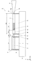
- FIG. 3 is a ZX sectional view of the external resonator type light emitting device 1.
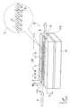
- FIG. 3 is a schematic perspective view of a grating element 9.
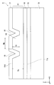
- FIG. 4 is a YZ sectional view of the grating element 9. It is ZX sectional drawing of the external resonator type light-emitting device 1A. It is YZ sectional drawing of the grating element 9A.
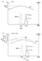
- 6 is a diagram showing a relationship between a gain curve of primary light emission in an active layer 5 and a reflectance profile of the grating element 9.
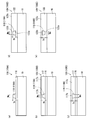
- FIG. 3 is a YZ sectional view of the grating element 109.
- FIG. 1 is a side sectional view schematically showing a configuration of an external resonator type light emitting device 1 according to a first embodiment of the present invention.
- the external resonator type light emitting device 1 mainly includes a light source element 2 that emits semiconductor laser light A by current injection and a grating element 9.
- the light source element 2 and the grating element 9 are provided to realize a resonator structure.
- the light source element 2 and the grating element 9 are mounted on one main surface of the flat common substrate 3.
- the common substrate 3 may be integrated, but a plurality of separate substrates may be joined.
- FIG. 1 is a ZX sectional view of the external resonator type light emitting device 1.
- the light source element 2 and the grating element 9 are mounted on the common substrate 3 in such a manner that a gap 14 is provided in the optical axis direction.
- Each end face of the light source element 2 and the grating element 9 may be cut obliquely in order to suppress end face reflection.
- the light source element 2 includes an active layer 5, a reflection film 6 provided on the outer surface of the active layer 5 (on the opposite side to the grating element 9), and a reflection provided on the end surface of the active layer 5 on the grating element 9 side.
- the light source element 2 oscillates alone (even without the grating element 9).
- the light source element 2 it is preferable to use an element that oscillates in a single mode in the longitudinal mode.
- the reflection characteristic depends on the wavelength as described later. Therefore, even if the longitudinal mode of the light source element 2 oscillates in multimode, the external resonator type light emitting device 1 can oscillate in single mode by controlling the wavelength characteristics. Is possible.
- the active layer 5 is provided on one main surface of the substrate 4, the reflective film is formed up to the side surface of the substrate 4, and the other main surface of the substrate 4 is a mounting surface for the common substrate 3.
- this is not an essential aspect, and an aspect in which the active layer 5 is provided directly on the common substrate 3 may be used.
- the active layer 5 it is preferable to use a GaAs-based semiconductor or an InP-based semiconductor. Specific materials and wavelengths can be selected as appropriate. For example, if a green laser that is the second harmonic is oscillated using a nonlinear optical element, a GaAs-based semiconductor that oscillates near a wavelength of 1064 nm is used for the active layer 5.
- the oscillation wavelength of the semiconductor laser light A may be 1100 nm or less, but is particularly preferably 990 nm or less.
- the wavelength of the semiconductor laser light A is shortened, the refractive index change of the semiconductor tends to be too large.
- the laser oscillation wavelength is particularly preferably 780 nm or more.
- the material of the reflection film 6 include a metal film such as gold.
- the reflective film 20 is preferably formed as a laminated film of oxides such as silicon dioxide, tantalum pentoxide, magnesium fluoride, and calcium fluoride.
- FIG. 2 is a schematic perspective view of the grating element 9.
- FIG. 3 is a YZ sectional view of the grating element 9.
- the grating element 9 generally has a configuration in which an optical material layer 11 is bonded to one main surface of a flat support substrate 10 by an adhesive layer 15.
- the other main surface of the support substrate 10 is a mounting surface of the grating element 9 with respect to the common substrate 3.
- the material of the support substrate 10 is not particularly limited, and examples thereof include glass such as lithium niobate, lithium tantalate, and quartz glass, crystal, Si, alumina, aluminum nitride, and silicon carbide.
- the optical material layer 11 has an incident surface 11a on which the semiconductor laser light A is incident and an output surface 11b that emits the output light B having a desired wavelength.
- the thickness Ts of the optical material layer 11 is preferably not less than 0.5 ⁇ m and not more than 3 ⁇ m.
- a pair of ridge grooves 19 which are linear grooves provided in parallel along the X-axis direction are provided, and a portion between the ridge grooves 19 is formed.
- An optical waveguide (ridge type optical waveguide) 18 is formed.
- the optical waveguide 18 is provided with the Bragg grating 12.
- the depth Tr of the ridge groove 19 is preferably 0.25 ⁇ m or more and 0.85 ⁇ m or less, and the width (size in the Y-axis direction) W m of the optical waveguide 18 is preferably 1.5 ⁇ m or more and 8 ⁇ m or less. . It is assumed that the width W m of the optical waveguide 18 is the width of the narrowest portion in the cross section of the optical waveguide 18 (a plane perpendicular to the optical axis direction of the semiconductor laser light A).
- the ridge groove 19 can be formed by physical processing such as dry etching using reactive ion etching, wet etching using hydrofluoric acid, cutting using an outer peripheral blade, laser ablation processing, or the like.
- the Bragg grating 12 is a periodic concavo-convex portion provided with a constant pitch ⁇ and a depth t d along the optical axis direction, as shown by a partially enlarged view E in FIG.
- the lengths of the convex part and the concave part in the optical axis direction are equal to ⁇ / 2.
- the Bragg grating 12 is shown along the ZX plane, but this is merely for convenience of explanation, and the Bragg grating 12 is actually formed along the XY plane.
- the pitch ⁇ is appropriately determined according to the wavelength of light desired to be emitted from the external resonator type light emitting device 1.
- the depth t d is suitably are 10nm or 250nm or less.
- the Bragg grating 12 reflects light based on a reflectance profile determined according to the pitch ⁇ under Bragg conditions.
- the wavelength ⁇ G of the main peak of the reflectance profile is a function of temperature that varies with the temperature coefficient d ⁇ G / dT.
- the reflectivity (grating reflectivity) in the Bragg grating 12, particularly the reflectivity at the wavelength ⁇ G of the main peak, is determined by the material for forming the optical material layer 11 (particularly its refractive index n b ), the pitch ⁇ of the Bragg grating 12, It is a value determined according to the value of the length L b and the depth t d .
- a grating reflectivity of 40% or less than 5% is achieved, which has a length L b of the Bragg grating 12 10 [mu] m or more It is realized by doing.
- the grating reflectance is preferably larger than the reflectance of the reflective film 6. If the grating reflectance is 5% or more, the output power is stable, but from the viewpoint of obtaining a large output power, the grating reflectance is more preferably 25% or less.
- the Bragg grating 12 may be provided on the lower surface 11 c side of the optical material layer 11. From the viewpoint of reducing variations in the shapes of the Bragg grating 12 and the ridge groove 19, it is preferable to form the Bragg grating 12 on the lower surface 11c so that the formation surfaces of the Bragg grating 12 and the ridge groove 19 are different.
- the Bragg grating 12 can be formed by physical or chemical etching. For example, a metal film such as Ni or Ti is formed on the upper surface of the optical material layer 11, and an etching mask is formed by periodically providing windows by photolithography. Then, the Bragg grating 12 is formed by etching the unmasked portion with a dry etching apparatus such as reactive ion etching and finally removing the metal mask.
- a dry etching apparatus such as reactive ion etching
- the Bragg grating 12 is provided separately from both the incident surface 11a and the exit surface 11b of the optical material layer 11. In particular, between the incident surface 11a and the Bragg grating 12, there is a propagation portion 13 in which no grating exists.
- the propagation part 13 is arranged to face the active layer 5 with a gap 14 interposed therebetween. However, from the viewpoint of shortening the length of the external resonator, the propagation unit 13 may be omitted.
- a lower buffer layer 16 and an upper buffer layer 17 are provided on the upper and lower surfaces of the optical material layer 11 as shown in FIG. Therefore, more strictly, the optical material layer 11 is provided on the support substrate 10 via the lower buffer layer 16.
- the lower buffer layer 16 and the upper buffer layer 17 may be omitted.
- the air layer is in direct contact with the Bragg grating 12, and therefore, the refractive index difference from where the Bragg grating 12 is not provided is greater than when the upper buffer layer 17 is provided. from while shortening the length L b of the Bragg grating 12, it is possible to increase the reflectivity.
- the lower buffer layer 16 and the upper buffer layer 17 are preferably made of, for example, silicon oxide.
- the lower buffer layer 16 and the upper buffer layer 17 can be formed on the substrate to be the optical material layer 11 by a known thin film forming method such as sputtering, vacuum deposition, or CVD.
- the optical material layer 11 is preferably configured using a substance having a refractive index nb of 1.8 or more and a thermal conductivity of 50 W / m ⁇ K or less.
- the optical material layer 11 By configuring the optical material layer 11 with a material having a refractive index nb of 1.8 or more, a high grating reflectance can be obtained while making the structure of the grating element 9 compact.
- the refractive index n b is more preferably 1.9 or more.
- the pitch ⁇ is too small Bragg grating since the formation of 12 is difficult, practically, although the refractive index n b is sufficient 4 or less, more preferably 3.6 or less.
- the equivalent refractive index of the region including the lower buffer layer 16 and the upper buffer layer 17 in the optical waveguide 18 is preferably 3.3 or less for the same reason.
- the support substrate 10 and the optical material layer 11 forming the grating element 9 are made of the above-described ceramics or glass material, a heat storage effect is obtained because the heat conduction is small. Thereby, the heat radiation of the semiconductor laser is suppressed, and the semiconductor laser is kept at a high temperature. Such a heat storage effect contributes to suppression of fluctuations in emission wavelength caused by changes in environmental temperature.
- the support substrate 10 and the optical material layer 11 are preferably formed of a material having a thermal conductivity of 25 W / m ⁇ K or less, and formed of a material of 10 W / m ⁇ K or less. Is most preferred.
- Mg magnesium
- Zn zinc
- Sc scandium
- In indium
- Mg magnesium
- Zn zinc
- Sc scandium
- In indium
- Mg magnesium
- Zn zinc
- Sc scandium
- In indium
- the aspect which contains rare earth elements as a dope component may be sufficient.
- the rare earth element Nd, Er, Tm, Ho, Dy, and Pr are particularly preferable.
- the adhesive layer 15 may be an aspect formed with an inorganic adhesive, an aspect formed with an organic adhesive, or an aspect formed with a combination of an inorganic adhesive and an organic adhesive. Also good.
- the support substrate 10 and the optical material layer 11 may be bonded together by direct bonding without forming the adhesive layer 15. In this case, a room temperature direct bonding method, a surface activation method, or an atomic diffusion bonding method can be employed.
- a mode in which a thin film layer to be the optical material layer 11 is formed on the support substrate 10 by a known thin film generation method such as sputtering, vacuum deposition, or CVD may be used.
- an antireflective film 7B is provided on the end surface on the incident surface 11a side of the optical material layer 11, and an antireflective film 7C is provided on the end surface on the output surface 11b side.
- the antireflective films 7B and 7C are preferably formed as a laminated film of an oxide such as silicon dioxide, tantalum pentoxide, magnesium fluoride, calcium fluoride, or a metal film.
- both the non-reflective films 7B and 7C may be provided as a layer having a smaller reflectance than the reflectance (grating reflectance) in the Bragg grating 12. Specifically, it is more preferably 0.1% or less.
- the principle of laser oscillation of the external resonator type light emitting device 1 having the above configuration will be outlined below.
- spontaneous emission light primary light emission
- the Bragg grating 12 reflects only light of a predetermined wavelength component that satisfies the Bragg condition among the primary light emission. 2 (reflected light C in FIG. 2), in the section from the reflective film 6 to the Bragg grating 12, oscillation (laser light) of light having a wavelength (oscillation wavelength) satisfying a predetermined phase condition occurs.
- the external resonator type light emitting device 1 can emit laser light having wavelength stability ensured in such a manner.
- a Fabry-Perot resonator can also be configured in the section between the reflective film 6 and the reflective film 20, but when the reflectance of the reflective film 20 is smaller than the reflectance of the grating, the distance from the reflective film 6 to the Bragg grating 12 is reached.
- the gain threshold can be made smaller in the resonator formed between the two. For this reason, the oscillation mode of the Bragg grating 12 becomes dominant.
- FIG. 4 is a ZX cross-sectional view of the external resonator type light emitting device 1A in which an antireflective film 7A is provided instead of the reflective film 20.
- the nonreflective film 7A may be provided in the same manner as the nonreflective films 7B and 7C.
- the configurations of the external resonator type light emitting device 1 and the external resonator type light emitting device 1A are the same except that the reflective film 20 and the nonreflective film 7A are different. Therefore, in the following description, unless otherwise specified, the external resonator type light emitting device 1 and the external resonator type light emitting device 1A will be described without any particular distinction.
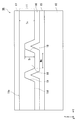
- FIG. 5 is a YZ sectional view of a grating element 9A, which is a modification of the grating element 9 shown in FIG.
- the grating element 9A has the same layer structure as the grating element 9, but the formation positions of the ridge groove 19 and the optical waveguide 18 are different. Specifically, a ridge groove 19 and an optical waveguide 18 are formed on the support substrate 10 side of the optical material layer 11 inside the element. Accordingly, the adhesive layer 15 has a convex portion corresponding to the portion of the ridge groove 19. Further, the upper surface 11e of the optical material layer 11 is a flat surface.
- the Bragg grating 12 may be formed on the upper surface 11e side which is a flat surface, or may be formed on the lower surface 11f side where the ridge groove 19 is provided.
- the Bragg grating 12 is formed on the upper surface 11e so that the formation surfaces of the Bragg grating 12 and the ridge groove 19 are different.
- the upper buffer layer 17 may not be provided in the grating element 9A.
- the difference in configuration between the grating element 9 and the grating element 9A is not directly related to the feature of the invention according to the present embodiment to be described later. Therefore, in the following description, unless otherwise specified, The grating element 9 and the grating element 9A will be described without any particular distinction. Further, the external resonator type light emitting device 1A shown in FIG. 4 may be provided with a grating element 9A.
- gain conditions and phase conditions which are conditions for emitting the emitted light B in the external resonator type light emitting device 1 according to the present embodiment, will be outlined.
- the gain condition is defined by the following equation (1).
- ⁇ t g th is a gain threshold value of the external resonator type light emitting device 1
- ⁇ a , ⁇ g , ⁇ m , and ⁇ b are the active layer 5, the gap 14, the propagation unit 13, and the Bragg grating 12, respectively.
- L a , L g , L m , and L b are the lengths of the active layer 5, the gap 14, the propagation unit 13, and the Bragg grating 12 in the optical axis direction, and r 1 and r 2 are respectively
- the reflectance of the reflective film 6 and the Bragg grating 12, and C out is the coupling efficiency between the grating element 9 and the light source element 2.
- Formula (1) indicates that if the gain of the resonator between the reflective film 6 and the Bragg grating 12 exceeds the loss represented by the right side, the laser oscillation and the emitted light B become the emitted light B. It represents that it is emitted to the outside. Since each variable on the right side has almost no wavelength dependence except for the reflectance r2 of the Bragg grating 12, the gain condition is actually determined according to the Bragg grating 12.
- ⁇ i 2 ⁇ n i / ⁇ (i is a, g, m).
- the length L a of the active layer 5 it is preferable that the viewpoint from 150 ⁇ m or more of increasing the power of the light emitted by B, as long 500 ⁇ m or less, it is preferable to 300 ⁇ m or less.
- the length of the gap 14 L g is preferably set to 1 ⁇ m or 10 ⁇ m or less. This is for oscillation stabilization.
- the length L b of the Bragg grating 12 is preferably from the viewpoint of reflectance 10 ⁇ m or more as described above, while preferably set to 300 ⁇ m or less. This has an effect of increasing the interval (longitudinal mode interval) ⁇ G TM of the wavelength ⁇ TM satisfying the phase condition of the equation (2), and contributes to mode hop suppression described later. From this viewpoint, it is more preferable that the length L b and 200 ⁇ m or less. Further, when the length Lb is short, the loss becomes small, so that the gain threshold value ⁇ t g th of the equation (1) can be reduced. As a result, driving with low current, low heat generation, and low energy is possible.
- the length L m of the propagating portion 13 is preferably a 100 ⁇ m or less. This promotes stable oscillation. Further, the length L m is preferably be at least 10 [mu] m, more preferably not less than 20 [mu] m.
- the length L WG grating element 9 in the optical axis direction is preferably set to 500 ⁇ m or less.
- the length LWG is more preferably 400 ⁇ m or less, and even more preferably 300 ⁇ m or less. Further, the length LWG is preferably 50 ⁇ m or more.
- FIG. 6 is a diagram showing the relationship between the primary emission gain curve in the active layer 5 and the reflectance profile of the grating element 9.
- FIG. 6A shows the case of a certain temperature Ta
- FIG. 6B shows the case of a temperature Tb higher than the temperature Ta.
- the temperatures Ta and Tb are both -10 ° C. or higher and 70 ° C. or lower.
- a temperature range of ⁇ 10 ° C. or more and 70 ° C. or less is particularly referred to as an assumed operation temperature range.
- movement assumption temperature range is a range assumed as the minimum as the temperature range of the environment where the external resonator type light-emitting device 1 which concerns on this Embodiment operate
- the gain of primary light emission has a temperature dependency associated with the temperature dependency of the band gap at least in the assumed operating temperature range.
- the center wavelength of the reflectance profile of the grating element 9 also has temperature dependence. More specifically, the gain of primary light emission is the maximum value of the gain while the peak value shifts to the longer wavelength side as the temperature of the light source element 2 (active layer 5) is higher, at least in the assumed operating temperature range. Is known to decrease. Further, it is known that the peak value (center wavelength ⁇ G ) of the reflection profile of the grating element 9 shifts to the longer wavelength side as the temperature of the grating element 9 increases, at least in the assumed operating temperature range. However, the shape of the reflectance profile can be regarded as almost constant regardless of the temperature.
- FIG. 6 also illustrates the reflectance profiles PF0 (a) and PF0 (b) of the Bragg grating used in the conventional external resonator type light emitting device for the cases of the temperatures Ta and Tb by broken lines. is doing.
- a Bragg grating is usually set (adjusted) so that the center wavelength at room temperature (20 ° C. to 30 ° C.) substantially coincides with the wavelength that gives the peak value of the gain curve at that temperature.
- the wavelength ⁇ 1 (a) giving the peak value Gp (a) in the gain curve GC1 is the center wavelength ⁇ g (a) of the reflectance profile PF0 (a).
- the wavelength ⁇ 1 (b) that gives the peak value Gp (b) in the gain curve GC2 and the center wavelength ⁇ g (b) of the reflectance profile PF0 (b) coincide with each other. do not do.
- the method of setting the Bragg grating as described above will be referred to as conventional setting.
- the gain of the emitted light becomes large at an environmental temperature where the peak position of the gain curve GC1 and the peak position of the reflectance profile coincide with each other.
- the peak shift of the gain curve is usually larger than the peak shift of the reflectance profile, so the difference between the two peak positions becomes larger and the reflection
- the value of the gain at the position in the rate profile is much lower than when the two match.
- the gain decreases from Gp (a) to Gg (b). That is, large gain fluctuations occur with changes in the environmental temperature.
- the gain shift is from Gp (a) to Gp (b) because the peak shift of the gain curve is directly the peak shift of the emitted light. Will be reduced. Also in this case, a large gain fluctuation occurs.
- the setting of the reflectance profile in the present embodiment takes into account gain fluctuations in the case of the conventional setting as described above.
- the Bragg grating 12 has a relationship of ⁇ 1 ⁇ G ⁇ G / 2.
- a reflectance profile is set (adjusted).
- FIG. 6 the relationship between the reflectance profile PF1 (a) at the temperature Ta and the reflectance profile PF1 (b) at the temperature Tb, which is indicated by a solid line, is shown.
- the wavelength range of the outgoing light B satisfying the phase condition is set in a range of ⁇ G ⁇ G / 2 to ⁇ G + ⁇ G / 2.
- a Fabry-Perot resonator can be configured even in the section between the reflective film 6 and the reflective film 20, but by setting the reflectance of the Bragg grating 12 larger than the reflectance of the reflective film 20.
- the gain threshold value of the resonator constituted by the Bragg grating 12 from the reflective film 6 can be reduced. For this reason, the oscillation mode of the Fabry-Perot resonator can be suppressed.
- the gain threshold of the Fabry-Perot resonator is further increased. Can be high. As a result, the oscillation mode of the Fabry-Perot resonator can be further suppressed.
- ⁇ G (Tmin) is the reflection wavelength of the Bragg grating at the lowest temperature of the assumed operation temperature
- ⁇ G (Tmax) is the reflection wavelength of the Bragg grating at the highest temperature of the assumed operation temperature.
- the difference value G (a) ⁇ G (b) can be made smaller than Gp (a) ⁇ Gg (b).
- ⁇ G ⁇ 1 ⁇ 5 nm at 50 ° C. or lower and ⁇ G ⁇ 1 ⁇ 10 nm at 20 ° C. or lower it is more preferable that ⁇ G ⁇ 1 ⁇ 5 nm at 50 ° C. or lower and ⁇ G ⁇ 1 ⁇ 10 nm at 20 ° C. or lower. In such a case, the fluctuation of the output of the emitted light can be suppressed to 3% or less of the output at room temperature within the assumed operating temperature range.
- G (a) -G (b) can be further reduced by using a material having a positive and large refractive index temperature dependency such as lithium niobate and lithium tantalate. Operation with less output fluctuation is possible.
- the external resonator type light emitting device 1 performs temperature control using a Peltier element or the like as in the conventional device. Wavelength-stable operation and power-stable operation can be realized without providing a power monitoring function.
- Mode hop suppression in the external resonator type light emitting device 1 will be described.
- Mode hop suppression in the present embodiment is realized from two viewpoints of limiting the wavelengths that can be taken by mode hops and expanding the temperature range in which mode hops do not occur. .
- the full width at half maximum ⁇ G of the main peak of the reflectivity profile 0.5nm or 3 It is set to a value larger than the conventional value of 0.0 nm or less. In other words, the main peak of the reflectance profile is broader than in the past.
- the main peak the number of longitudinal modes that fall within the scope of the full width at half maximum ⁇ G around the wavelength lambda G (the number of wavelength lambda TM) is set to 2 to 5.
- the spectral width of the laser-oscillated output is 0.1 nm or less.
- the wavelength variation falls within the range of ⁇ G. That is, large wavelength fluctuations do not occur.
- the temperature T mh at which the mode hop occurs is expressed by the following equation (3).
- ⁇ G TM in equation (3) is an interval (longitudinal mode interval) of the wavelength ⁇ TM that satisfies the phase condition in equation (2) as described above, but since ⁇ TM can take a plurality of values, ⁇ G TM can also take a plurality of values.
- d ⁇ G / dT is the temperature coefficient of the wavelength ⁇ G of the main peak in the reflectance profile of the grating reflectance as described above
- d ⁇ TM / dT is the outgoing light B that satisfies the phase condition of Expression (2). Is the temperature coefficient of the wavelength ⁇ TM.
- the refractive index n b of the optical material layer 11 is 1.8 or more as described above, the temperature coefficient d ⁇
- equation (4) is satisfied. It is more preferable that the value on the left side of the formula (4) is 0.025 or less.
- a pair of ridge grooves 19 are provided in the optical material layer 11 so that a ridge type optical waveguide 18 is provided in the grating element 9.
- the optical material layer 11 also exists in portions other than the optical waveguide 18, specifically, below and on the side of the ridge groove 19.
- the mode of providing the optical waveguide as a ridge-type optical waveguide is not limited to this.
- a ridge-type optical waveguide made of a material (hereinafter also simply referred to as an optical material) having a refractive index nb of 1.8 or more is the same as the material constituting the optical material layer 11.
- a grating element provided in a mode different from the above embodiment will be described.
- FIG. 7 is a YZ cross-sectional view of various grating elements 109 (109A to 109E) according to the present embodiment.
- a ridge-type optical waveguide 118 is formed of an optical material and has an elongated core extending in the X-axis direction.
- the optical waveguide 118 is common in that the YZ section (hereinafter also referred to as a transverse section) forms a convex figure.
- the ridge type optical waveguide 118 is made of an optical material in the various grating elements 109A to 109E according to the present embodiment.
- the YZ section of the optical waveguide 118 has a convex shape means that the line segment connecting any two points of the outer contour line of the transverse section of the optical waveguide 118 is inside the outer contour line of the transverse section. Means to be located.
- convex figures include polygons such as triangles, quadrilaterals, hexagons, and octagons, circles, and ellipses. Among these, a quadrangle having an upper side, a lower side, and a pair of side surfaces is preferable, and a trapezoid is particularly preferable.
- the optical waveguide 118 of the grating element 109 is also in the same manner as the optical waveguide 18 of the grating element 9 provided in the external resonator type light emitting device 1 according to the first embodiment.
- the Bragg grating 12 and the propagation unit 13 are provided.
- non-reflective films similar to the non-reflective films 7B and 7C included in the grating element 9 are provided at both ends of the optical waveguide 118 in the X-axis direction.
- the external resonator type light emitting device configured using the grating element 109 is configured by replacing the grating element 9 of the external resonator type light emitting device 1 according to the first embodiment with the grating element 109. The That is, all the requirements regarding the oscillation of the laser light in the grating element 109 are the same as the requirements in the grating element 9 according to the first embodiment.
- a grating element 109A shown in FIG. 7A has a configuration in which a buffer layer (first buffer layer) 116 is provided on a support substrate 10, and an optical waveguide 118 (118A) is provided on the buffer layer 116.
- the optical waveguide 118A has a trapezoidal shape in which the cross section is longer in the lower base than in the upper base. That is, in the optical waveguide 118A, the upper side surface facing the lower side surface is narrower than the lower side surface in contact with the buffer layer 116.
- the width W m of the optical waveguide 118A is 1.5 ⁇ m or more 8 ⁇ m or less according.
- T h (the height in the Z-axis direction) thickness of the optical waveguide 118A is preferably a 0.5 [mu] m ⁇ 3 [mu] m.
- the maximum width of the optical waveguide 118A is preferably 0.7 ⁇ m or more and 9 ⁇ m or less.
- the first buffer layer 116 is formed to a thickness of about 0.2 ⁇ m to 2 ⁇ m with a material selected from materials having a refractive index smaller than that of the optical material, such as SiO 2 , alumina, polyimide, and epoxy resin.
- the buffer layer 116 and the air (air layer) existing around the optical waveguide 118 function as a clad having a relatively lower refractive index than the optical waveguide 118 serving as the core.
- the buffer layer 116 and the optical waveguide 118A in the grating element 109A are sequentially formed by a known thin film forming method such as sputtering, vacuum deposition, and CVD, and the thin film layer made of an optical material constituting the optical waveguide 118A. Then, the latter unnecessary portion can be removed by etching. In addition, the aspect which forms the Bragg grating 12 in the case of the etching concerned may be sufficient.
- the grating element 109B shown in FIG. 7B further includes a buffer layer (second buffer layer) 117 that covers the optical waveguide 118A from above and from the side in the grating element 109A shown in FIG. 7A. It has a configuration. Similar to the first buffer layer 116, the second buffer layer 117 may be formed of a material selected from, for example, SiO 2 , alumina, polyimide, epoxy resin, etc., but is different from the first buffer layer 116. It is made of a material. The second buffer layer 117 is formed so that the thickness of the upper portion 117b of the optical waveguide 118 is about 0.2 ⁇ m to 2 ⁇ m.
- a buffer layer 116 and an optical waveguide 118A are formed in the same manner as in the case of forming the grating element 109A. Further, after the Bragg grating 12 is formed, a known thin film formation such as sputtering, vacuum evaporation, or CVD is formed. This can be done by forming the buffer layer 117 by a technique.
- the grating element 109C shown in FIG. 7C includes an optical waveguide 118B provided so as to have a trapezoidal shape in which the horizontal cross section is shorter than the upper base, and the grating shown in FIG. 7B.
- the structure is similar to that of the element 109B.
- the lower side surface in contact with the first buffer layer 116 is narrower than the upper side surface facing the lower side surface.
- the arrangement mode of the optical waveguide 118B corresponds to a configuration in which the optical waveguide 118A is turned upside down.
- the formation of the grating element 109C can be performed in the same manner as the formation of the grating element 109B, except that the etching conditions for etching a thin film layer made of an optical material are different.
- the aspect which has the structure which the grating element 109 is provided with the optical waveguide 118B which does not comprise the 2nd buffer layer 117 may be sufficient. This corresponds to a vertically inverted optical waveguide 118A of the grating element 109A.
- each of the grating elements 109D and 109E shown in FIGS. 7D and 7E has a configuration in which a buffer layer 122 made of one material is provided around the optical waveguide 118A or 118B.
- the buffer layer 122 may be formed of a material selected from SiO 2 , alumina, polyimide, epoxy resin, and the like.
- the grating elements 109D and 109E are formed in the same procedure as the grating elements 109B and 109C, the buffer layer 122 is formed for the portion corresponding to the first buffer layer 116, and the optical waveguide 118A or 118B is formed.
- the remaining portion of the buffer layer 122 can be formed in the same manner as the second buffer layer 117.
- the lower portion 122a of the optical waveguide 118 has the same thickness as the first buffer layer 116 of the grating elements 109A to 109C, and the upper portion 122b of the optical waveguide 118 has a thickness of the grating element 109A.
- the second buffer layer 117 of ⁇ 109C is formed to have the same thickness as the upper portion 117b of the optical waveguide 118.
- the buffer layer 116, 117, or 122 is formed so as to cover substantially the entire surface of the support substrate 10, this is an essential aspect. Absent.
- the support substrate 10 may be partially exposed as long as the buffer layer 116 exists at least below the optical waveguide 118A.
- the grating elements 109B to 109E if the periphery of the optical waveguide 118A or 118B is covered, the side portion 117c or 122c of the optical waveguide 118 needs to be provided so as to cover the entire support substrate 10.
- the support substrate 10 may be partially exposed.
- the grating element 109 it can be formed by bonding with the adhesive layer 15 as in the case of the grating element 9 according to the first embodiment.
- a buffer layer 116 is formed in advance on a substrate made of an optical material to be the optical waveguide 118A by sputtering or the like, and then the buffer layer 116 and the base substrate 10 are formed.
- the optical waveguide 118 may be formed by bonding with the adhesive layer 15 and then etching.
- a buffer layer is further provided above the optical waveguide 118 such as the grating elements 109B to 109E, this may be performed after the etching and the Bragg grating 12 are formed.
- the grating element 109 has the same configuration as the reflection wavelength setting mode in the grating element 9 in the first embodiment.
- the reflection wavelength it is possible to perform wavelength stable operation and power stable operation without performing temperature control using a Peltier element, etc., or even having a power monitoring function, as was done in conventional devices. Is realized.
- the optical material layer 11 may be formed on the support substrate 10 as a thin film layer.
- Examples of the method for forming the thin film layer include sputtering, vapor deposition, and CVD. In this case, since the optical material layer 11 is directly formed on the support substrate 10, it is not necessary to form the adhesive layer 15.
- Each end face of the light source element 2 and the grating element 9 may be cut obliquely for the purpose of suppressing end face reflection.
- light sources such as laser arrays arranged one-dimensionally instead of the light source elements 2 described above.
- a super luminescence diode or a semiconductor optical amplifier (SOA) may be used as the light source element 2.
- Example 1 A grating element 9A shown in FIG. 5 was produced and its characteristics were evaluated.
- a metal Ti film is formed as a mask on one main surface of the crystal substrate, and the pattern ⁇ is 225 nm, the length L b is 150 ⁇ m, and the depth is t d by patterning by a photolithography technique and fluorine-based reactive ion etching.
- a grating pattern to be a Bragg grating 12 having a thickness of 15 nm was formed. At the time of patterning, the length L m of the propagating portion 13 was set to be 20 [mu] m.
- the lower buffer layer 16 made of SiO 2 was formed to a thickness of 0.5 ⁇ m on the surface on which the ridge groove 19 was formed by a sputtering apparatus.
- a black LN substrate was prepared as the support substrate 10, and one main surface thereof and the lower buffer layer 16 were bonded to obtain a laminate.
- the adhesive layer 15 was formed using an epoxy resin.
- the non-adhesive surface side of the black LN substrate is attached to a polishing surface plate, the other main surface of the exposed LN substrate (the surface where the Bragg grating is not formed) is precisely polished, and the thickness Ts of the optical material layer 11 is obtained.
- the laminate was removed from the polishing surface plate, and an upper buffer layer 17 made of SiO 2 was formed to a thickness of 0.5 ⁇ m on the polishing surface by a sputtering apparatus.
- the optical characteristics at room temperature (20 ° C.) of the obtained grating element 9A were evaluated. Specifically, using a super luminescence diode (SLD) that is a broadband wavelength light source, TE mode light is input to the grating element 9A, and the output light is analyzed with an optical spectrum analyzer, and the obtained transmission is obtained. From the characteristics, the reflection characteristics of the grating element 9A were evaluated.
- SLD super luminescence diode
- the grating element 9A was mounted to produce the external resonator type light emitting device 1 of FIG.
- a GaAs laser in which the active layer 5 is made of GaAs, the reflectance of the reflective film 6 is 97%, and the reflectance of the reflective film 20 is 3% is prepared as the light source element 2.
- the center wavelength of the laser light (primary light emission) emitted from the light source element 2 at room temperature was 980 nm, and the output was 60 mW.
- the distance L g between the light source element 2 and the grating element 9 was 1 [mu] m.
- the wavelength 990 corresponding to the central wavelength ⁇ G of the reflection profile of the Bragg grating 12 at room temperature.
- An oscillation light (emitted light B) oscillating at .9 nm was obtained.
- the output (laser output) was 40.1 mW, which is smaller than the output of primary light emission.
- the difference in the laser output of the oscillation light (emitted light B) between 20 ° C. and 70 ° C. is 0.5 mW at the maximum, and the oscillation wavelength ⁇ TM is The maximum difference was 5.2 nm.
- the maximum laser output difference of the oscillation light (emitted light B) between 20 ° C. and 70 ° C. is 0.5 mW
- the oscillation wavelength ⁇ TM is The maximum difference was 5.0 nm.
- Example 3 the grating element 9 including the optical material layer 11 as a thin film layer was formed.
- a grating pattern to be the Bragg grating 12 with t d 40 nm was formed.
- the laminate was cut into a bar shape in which the extending direction of the black grating was the longitudinal direction using a dicing apparatus. After the cut surface was optically polished, an AR coating having a reflectance of 0.1% was formed as the antireflective films 7B and 7C. Finally, the grating element 9 was obtained by cutting the chip.
- the wavelength ⁇ 1 of the primary light emission in the external resonator type light emitting device 1 was measured in Table 3.
- the temperature coefficient d ⁇ TM / dT of the oscillation light was 0.05 nm / ° C., and the formula (4) was satisfied.
- the difference in laser output of the oscillation light (emitted light B) between 20 ° C. and 70 ° C. is 2.2 mW at the maximum, and the oscillation wavelength ⁇ TM is The difference was a maximum of 2.1 nm.
- the grating element 9A and the external resonator type light emitting device 1A were manufactured and evaluated in the same procedure as in Example 1 except that the pitch ⁇ of the Bragg grating 12 was set to 222 nm.
- the results of the laser output were measured in Table 4.
- the temperature coefficient d ⁇ TM / dT of the oscillation light was 0.05 nm / ° C., and the formula (4) was satisfied.
- the maximum laser output difference of the oscillation light (emitted light B) between 20 ° C. and 70 ° C. is 9.6 mW, and the oscillation wavelength ⁇ TM is The maximum difference was 5.0 nm.
Landscapes
- Physics & Mathematics (AREA)
- Condensed Matter Physics & Semiconductors (AREA)
- General Physics & Mathematics (AREA)
- Electromagnetism (AREA)
- Optics & Photonics (AREA)
- Semiconductor Lasers (AREA)
- Diffracting Gratings Or Hologram Optical Elements (AREA)
Abstract
高い波長安定性が確保されるとともに、光出力変動が抑制されてなる外部共振器型発光装置を実現する。外部共振器型発光装置が、レーザ光を発する活性層を有する半導体レーザ光源と、活性層から発せられたレーザ光の光軸方向を長手方向とするリッジ型光導波路を備えるとともに、光導波路の途中に設けられたブラッググレーティング(BG)を備えており、入射したレーザ光のうち所定の波長成分の光を半導体レーザ光源とBGとの間で発振させて装置外部への出射光として出射するグレーティング素子と、を備え、半導体レーザ光源から発せられるレーザ光の波長をλ1とし、BGの反射率プロファイルの中心波長をλGとし、半値全幅をΔλGとするときに、少なくとも-10℃以上30℃以下においてλ1<λG-ΔλG/2であるとともに、出射光の波長域がλG-ΔλG/2以上λG+ΔλG/2以下であるようにした。
Description
本発明は、グレーティング素子を用いた外部共振器型発光装置に関する。
一般に、半導体レーザとしては、両端面に形成したミラーで活性層を挟むことにより光共振器を構成してなる、ファブリ-ペロー(FP)型のものが採用されている。しかしながら、このFP型レーザは、定在波条件が成立する波長で発振するために、縦モードが多モードになりやすい。特に電流や温度が変化すると発振波長が変化し、それにより光強度が変化するという性質がある。
一方、光通信やガスセンシングなどの分野では、波長安定性の高い単一モード発振のレーザが必要とされている。係る要求を満たすべく、波長安定性のある半導体レーザとして、分布帰還型(DFB)レーザや分布反射型(DBR)レーザが開発されてなる。これらのレーザは、半導体中にグレーティング(回折格子)を設け、その波長依存性を利用して特定の波長のみを発振させるものである。
例えば、DBRレーザとして、活性層の導波路の延長上の導波路面に凹凸を形成しブラッグ反射によるミラーを設けた構成の共振器を備えるものが既に公知であり、その一態様として、グレーティングを半導体の中にモノリシックに形成した構成のものが広く知られている(例えば、特許文献1および特許文献2参照)。係るDBRレーザにおいては、光導波層の両端にグレーティングが設けられているため、活性層で発せられた光は光導波層を伝搬し、その一部が該グレーティングで反射されて電流注入部に戻り、増幅される。係るDBRレーザにおいては、特定の波長の光だけが、グレーティングによって決められた方向に反射されるので、レーザ光の波長は一定になる。すなわち、ブラッグ反射を利用した波長選択性のあるミラーによって、レーザ光の一部を半導体レーザに帰還させることにより、波長安定動作が実現されている。
また、DBRレーザの応用として、グレーティングを半導体とは異なる部品であるグレーティング素子として設けることで、外部で共振器を形成する、外部共振器型半導体レーザが開発されている。このタイプの半導体レーザは、波長安定性、温度安定性、制御性がよいという特徴がある。外部共振器としては、ファイバ・ブラッグ・グレーティング(FBG)や、ボリューム・ホログラム・グレーティング(VHG)がある(非特許文献1および非特許文献2参照)。これらの半導体レーザは、グレーティングを半導体とは別部材で構成してなるので、反射率、共振器長を個別に設計できるというメリットがあり、電流注入による発熱による温度上昇の影響を受けないので、波長安定性をさらに良くすることができるという効果を奏する。また、半導体とは屈折率の温度変化が異なるので、共振器長と合わせて設計することにより、温度安定性を高めることができる、という効果も得られる。
例えば、グレーティングを石英ガラスからなる導波路に形成してなる外部共振器型レーザが公知である(例えば、特許文献3参照)。特許文献3に開示されている外部共振器型レーザは、室温が大きく変化する(例えば30℃以上)環境においても温度コントローラを使用することなく使える、周波数安定化レーザ(温度無依存レーザ)である。
また、半導体レーザとグレーティング素子との組み合わせでパワーの安定化を行う方法も既に公知である(例えば、非特許文献3参照)。
また、半導体レーザにおいては、温度が上昇すると最大のゲインが低下し、かつ、発振閾値電流が上昇する、という点も公知である(例えば、非特許文献4および非特許文献5参照)。非特許文献4および非特許文献5には、半導体レーザを電流一定駆動させた場合には、環境温度が変動した場合に光出力が変動することも示唆されている。
また、非特許文献1には、半導体レーザにおいて生じる、温度上昇に伴って波長安定性を損なう現象であるモードホップのメカニズムと、その改善策について言及がある。
さらには、SiO2、SiO1-xNx(0.55≦x≦0.65)、あるいはSiとSiNとをコア層とする光導波路、およびこの光導波路にグレーティングを形成した外部共振器型レーザであって、精密な温度制御なしで発振波長を一定に保つことができるものがすでに公知である(例えば、特許文献4参照)。特許文献4に開示されてなる外部共振器型レーザにおいては、回折格子の反射波長の温度変化率(ブラッグ反射波長の温度係数)を小さくすることが前提条件とされてなる。特許文献4にはさらに、係る外部共振器レーザにおいてレーザ発振を縦モードマルチモードとすることでパワー安定性を実現できることも記載されている。
また、石英、InP、GaAs、LiNbO3、LiTaO3、ポリイミド樹脂からなる光導波路に形成したグレーティングを利用した外部共振器レーザもすでに公知である(例えば、特許文献5参照)。特許文献5には、係る態様の外部共振器レーザにおいて光源である半導体レーザの光射出面における反射率が実効反射率Re(実質的に0.1~38.4%)となる場合に、レーザ発振を縦モードマルチモードとすることでパワー安定性を実現できることが記載されている。
半導体レーザにおいては、使用中に温度や注入電流が変化すると、ゲインや共振器の条件が代わることによって発振波長が変化し、キンクといわれる、光パワーが変動する現象が生じる。例えば、FP型のGaAs半導体レーザの場合、通常、発振波長が0.3nm/℃の温度係数で変化する。
また、使用中の温度上昇によって、共振器内の発振モード(縦モード)が、あるモードから違うモードに移る、モードホップと呼ばれる現象が生じ得ることも知られている。例えば、FP型のGaAs半導体レーザの場合、モードホップが生じると、上述の温度係数に従う変化よりもさらに大きな波長変動が起こり、それと同時に、出力が5%以上変動することが知られている。
このような波長の変化を抑制するには、半導体レーザを所定の温度範囲内(例えば、非特許文献1においてΔTallとされている温度範囲)で使用する必要がある。そこで、従来の半導体レーザにおいては、ペルチェ素子を使用して半導体レーザの温度を制御している。ペルチェ素子の使用は、部品点数が多くなるととともにモジュールのサイズが大きくなるため、コスト高の要因となっている。
また、特許文献3に開示された外部共振器型レーザにおいては、温度無依存にするために、従来の共振器構造はそのままに、光導波路層に応力を与えることによって熱膨張に起因する温度係数を補償することにより、温度無依存性およびモードホップの抑制が実現されている。具体的には、素子に金属板を貼りつけ、さらに導波路中に温度係数を調整する層を付加させている。このため、共振器構造が、さらに大きくなるという問題がある。
電子情報通信学会論文誌 C‐II Vol.J81, No.7 pp.664-665, 1998年7月
電子情報通信学会技術研究報告 LQE, 2005年 105巻 52号 pp.17-20
古河電工時報 平成12年1月 第105号 p24-29
M.Asada,etal, "Gainand intervalence band absorption in quantum-well lasers", IEEE J. Quantumn Electron, QE-2(7), p.745-753, 1984.
Y.Suematsu, A.R.Adams, "Handbook of semiconductor lasers and photonic integrated circuits", Ohmsha Ltd.,p.334-337, 1994.
本発明は上記課題に鑑みてなされたものであり、ペルチェ素子による温度制御を行わずとも、高い波長安定性が確保されるとともに、光出力変動が抑制されてなる外部共振器型発光装置を実現することを目的とする。
上記課題を解決するため、本発明の第1の態様では、外部共振器型発光装置が、レーザ光を発する活性層を有する半導体レーザ光源と、前記活性層から発せられた前記レーザ光の光軸方向を長手方向とするリッジ型光導波路を備えるとともに、前記リッジ型光導波路の途中に設けられたブラッググレーティングを備えており、入射した前記レーザ光のうち所定の波長成分の光を前記半導体レーザ光源と前記ブラッググレーティングとの間で発振させて前記外部共振器型発光装置の外部への出射光として出射するグレーティング素子と、を備え、前記半導体レーザ光源から発せられる前記レーザ光の波長をλ1とし、前記ブラッググレーティングの反射率プロファイルの中心波長をλGとし、前記反射率プロファイルの半値全幅をΔλGとするときに、少なくとも-10℃以上30℃以下においてλ1<λG-ΔλG/2であるとともに、前記出射光の波長域がλG-ΔλG/2以上λG+ΔλG/2以下である、ようにした。
本発明の第2の態様では、第1の態様に係る外部共振器型発光装置において、50℃以下においてλG-λ1≧5nmであり、20℃以下においてλG-λ1≧10nmである、ようにした。
本発明の第3の態様では、第1または第2の態様に係る外部共振器型発光装置において、前記グレーティング素子が、支持基板と、前記支持基板上に設けられてなり0.5μm以上3.0μm以下の厚みを有する光学材料層と、前記支持基板と前記光学材料層とを接合する接合層と、を備えており、前記リッジ型光導波路が前記光学材料層に設けられており、前記半導体レーザ光の光軸方向における前記ブラッググレーティングの長さをLbとし、前記ブラッググレーティングを構成する凹凸の深さをtdとするときに、10μm≦Lb≦300μmかつ10nm≦td≦250nmであるようにした。
本発明の第4の態様では、第3の態様に係る外部共振器型発光装置において、前記光学材料層の材質が、ガリウム砒素、ニオブ酸リチウム、酸化タンタル、タンタル酸リチウム、酸化亜鉛および酸化アルミナからなる群より選択される、ようにした。
本発明の第5の態様では、第1または第2の態様に係る外部共振器型発光装置において、前記グレーティング素子が、支持基板の上に前記リッジ型光導波路を備える構成を有するものであり、前記リッジ型光導波路が、前記長手方向に垂直な断面が凸図形をなすとともに0.5μm以上3.0μm以下の厚みを有してなり、前記半導体レーザ光の光軸方向における前記ブラッググレーティングの長さをLbとし、前記ブラッググレーティングを構成する凹凸の深さをtdとするときに、10μm≦Lb≦300μmかつ10nm≦td≦250nmである、ようにした。
本発明の第6の態様では、第5の態様に係る外部共振器型発光装置において、前記リッジ型光導波路の材質が、ガリウム砒素、ニオブ酸リチウム、酸化タンタル、タンタル酸リチウム、酸化亜鉛および酸化アルミナからなる群より選択される、ようにした。
本発明の第7の態様では、第1ないし第6の態様のいずれかに係る外部共振器型発光装置であって、前記半導体レーザ光の光軸方向における前記グレーティング素子の長さをLWGとするときに、LWG≦500μmであることを特徴とする。
本発明の8の態様では、第7の態様に記載の外部共振器型発光装置において、0.5nm≦ΔλG≦3.0nmであるようにした。
本発明の第9の態様では、第1ないし第8の態様のいずれかに係る外部共振器型発光装置において、前記波長域に、前記出射光の波長となる波長値が2以上5以下存在する、ようにした。
本発明の第10の態様では、第1ないし第9の態様のいずれかに係る外部共振器型発光装置において、ブラッグ波長の温度係数をdλG/dTとし、前記出射光の波長の温度係数をdλTM/dTとするときに、
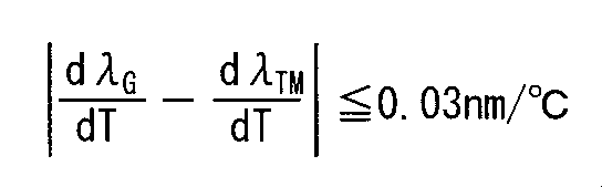
であるようにした。
本発明の第1ないし第10の態様によれば、動作想定温度範囲内において環境温度が変化したとしても、波長変動および出力変動の抑制された外部共振器型発光装置1が実現される。
<第1の実施の形態>
<外部共振器型発光装置の構成>
図1は、本発明の第1の実施の形態に係る外部共振器型発光装置1の構成を模式的に示す側断面図である。外部共振器型発光装置1は、電流の注入によって半導体レーザ光Aを発する光源素子2と、グレーティング素子9とを主として備える。外部共振器型発光装置1においては、これら光源素子2とグレーティング素子9とが備わることで、共振器構造が実現されてなる。光源素子2とグレーティング素子9とは、平板状の共通基板3の一方主面上にマウントされている。共通基板3は一体であってよいが、複数個の別体の基板を接合したものであってもよい。
<外部共振器型発光装置の構成>
図1は、本発明の第1の実施の形態に係る外部共振器型発光装置1の構成を模式的に示す側断面図である。外部共振器型発光装置1は、電流の注入によって半導体レーザ光Aを発する光源素子2と、グレーティング素子9とを主として備える。外部共振器型発光装置1においては、これら光源素子2とグレーティング素子9とが備わることで、共振器構造が実現されてなる。光源素子2とグレーティング素子9とは、平板状の共通基板3の一方主面上にマウントされている。共通基板3は一体であってよいが、複数個の別体の基板を接合したものであってもよい。
なお、図1および以降の図面においては、光源素子2からの半導体レーザ光Aの出射は水平面内においてなされるものとする。そして、これらの図面においては、係る半導体レーザ光Aの光軸方向をX軸方向とし、水平面内においてX軸方向と垂直な方向をY軸方向とし、鉛直方向をZ軸方向とする、右手系のXYZ座標を付している。従って、より詳細にいえば、図1は外部共振器型発光装置1のZX断面図である。
光源素子2とグレーティング素子9とは、光軸方向において間隙14を設ける態様にて、共通基板3にマウントされる。なお、光源素子2とグレーティング素子9の各端面は、それぞれ、端面反射を抑制するために斜めカットされていてもよい。
光源素子2は、活性層5と、活性層5の外側(グレーティング素子9とは反対側)の端面に設けられた反射膜6と、活性層5のグレーティング素子9側の端面に設けられた反射膜20とを備える。反射膜20の反射率はグレーティングの反射率よりも小さい。
光源素子2は単独で(グレーティング素子9がなくても)レーザ発振するものである。光源素子2としては、縦モードがシングルモード発振するものを用いるのが好ましい。しかし、光源素子2に加えてグレーティング素子9を備えることで外部共振器型レーザとしての構成を有する本実施の形態に係る外部共振器型発光装置1においては、後述するように反射特性に波長依存性を持たせることができることから、その波長特性を制御することにより、光源素子2の縦モードがマルチモード発振する場合であっても、外部共振器型発光装置1としてはシングルモード発振することが可能である。
なお、図1においては活性層5が基体4の一方主面上に設けられるとともに反射膜が基体4の側面にまで形成され、かつ、該基体4の他方主面が共通基板3に対する載置面となる場合を例示しているが、これは必須の態様ではなく、活性層5が直接に共通基板3上に設けられる態様であってもよい。
活性層5としては、GaAs系半導体やInP系半導体を用いるのが好適である。具体的な材質や波長は適宜選択できる。例えば、非線形光学素子を利用して第2高調波である緑色レーザを発振させる場合であれば、波長1064nm付近で発振するGaAs系半導体を活性層5に用いることになる。
なお、光源素子2から出射される半導体レーザ光Aの波長が長くなると、ブラッグ波長の温度変化が大きくなる傾向がある。波長安定性を高めるという観点からは、半導体レーザ光Aの発振波長は1100nm以下であればよいが、990nm以下であることが特に好ましい。一方、半導体レーザ光Aの波長が短くなると、半導体の屈折率変化が大きくなりすぎる傾向がある。波長安定性を高めるためには、レーザの発振波長は780nm以上が特に好ましい。
また、反射膜6の材質としては、金などの金属膜などが例示される。一方、反射膜20は、二酸化珪素、五酸化タンタル、フッ化マグネシウム、フッ化カルシウムなどの酸化物の積層膜として形成するのが好適である。
図2は、グレーティング素子9の概略斜視図である。図3は、グレーティング素子9のYZ断面図である。
図1においては図示を省略しているが、グレーティング素子9は、概略、平板状の支持基板10の一方主面上に、光学材料層11を接着層15によって接合させた構成を有する。なお、支持基板10の他方主面が共通基板3に対するグレーティング素子9の載置面となっている。支持基板10の材質は特に限定されず、ニオブ酸リチウム、タンタル酸リチウム、石英ガラス等のガラス、水晶、Si、アルミナ、窒化アルミニウム、炭化ケイ素などを例示することができる。
光学材料層11は、半導体レーザ光Aが入射する入射面11aと所望波長の出射光Bを出射する出射面11bとを有する。光学材料層11の厚みTsは、0.5μm以上3μm以下であるのが好ましい。
また、光学材料層11の上面11d側には、X軸方向に沿って平行に設けられた直線状の溝部である1対のリッジ溝19が設けられてなり、リッジ溝19の間の部分が光導波路(リッジ型光導波路)18とされてなる。そして、係る光導波路18に、ブラッググレーティング12が設けられてなる。リッジ溝19の深さTrは、0.25μm以上0.85μm以下であるのが好ましく、光導波路18の幅(Y軸方向のサイズ)Wmは1.5μm以上8μm以下であるのが好ましい。なお、光導波路18の幅Wmとは、光導波路18の横断面(半導体レーザ光Aの光軸方向に垂直な面)において最も狭い部分の幅であるとする。
リッジ溝19は、例えば、反応性イオンエッチングによるドライエッチング、フッ硝酸によるウエットエッチング、外周刃による切削加工やレーザアブレーション加工などによる物理的な加工によって形成が可能である。
ブラッググレーティング12は、図2において部分拡大図Eにて示すように、光軸方向に沿って一定のピッチΛおよび深さtdで設けられた周期的な凹凸部である。光軸方向における凸部と凹部の長さは等しくΛ/2である。なお、図1においてはZX平面に沿ってブラッググレーティング12を示しているがこれはあくまで説明の都合に過ぎず、実際には、ブラッググレーティング12はXY平面に沿って形成される。
ピッチΛは、外部共振器型発光装置1から出射させたい光の波長に応じて適宜に定められる。一方、深さtdは、10nm以上250nm以下とされるのが好適である。
ブラッググレーティング12においては、ブラッグ条件のもと、ピッチΛに応じて定まる反射率プロファイルに基づき光が反射される。なお、反射率プロファイルの主ピークの波長λGは温度係数dλG/dTで変化する温度の関数となる。また、ブラッググレーティング12における反射率(グレーティング反射率)、特に主ピークの波長λGにおける反射率は、光学材料層11の形成材料(特にその屈折率nb)や、ブラッググレーティング12のピッチΛ、長さLb、深さtdの値などに応じて定まる値である。
外部共振器型発光装置1における発振を促進するという観点からは、5%以上40%以下というグレーティング反射率が実現されるのが好ましく、これは、ブラッググレーティング12の長さLbを10μm以上とすることによって実現される。また、グレーティング反射率は反射膜6の反射率よりも大きい方が好ましい。なお、グレーティング反射率が5%以上であれば出力パワーは安定するが、大きな出力パワーを得るという観点からは、グレーティング反射率は25%以下がより好ましい。
なお、ブラッググレーティング12は、光学材料層11の下面11cの側に設けられる態様であってもよい。ブラッググレーティング12とリッジ溝19の形状ばらつきを低減するという観点からは、ブラッググレーティング12を下面11c上に形成することによって、ブラッググレーティング12とリッジ溝19の形成面を違える方が好ましい。
ブラッググレーティング12は、物理的あるいは化学的なエッチングにより形成することができる。例えば、Ni、Tiなどの金属膜を光学材料層11の上面に成膜し、フォトリソグラフィーにより周期的に窓を設けることによってエッチング用マスクを形成する。その後、マスクされていない箇所を反応性イオンエッチングなどのドライエッチング装置でエッチングし、最後に金属マスクを除去することにより、ブラッググレーティング12が形成される。
ブラッググレーティング12は、光学材料層11の入射面11aおよび出射面11bのいずれからも離隔して設けられてなる。特に、入射面11aとブラッググレーティング12との間は、グレーティングが存在しない伝搬部13となっている。伝搬部13は、間隙14を介して活性層5と対向配置されてなる。ただし、外部共振器の長さを短くするという観点からは、伝搬部13はなくてもよい。
なお、図2では図示を省略しているが、図3に示すように、光学材料層11の上下面に下側バッファ層16と上側バッファ層17とが設けられる。従って、より厳密には、光学材料層11は下側バッファ層16を介して支持基板10上に設けられる。
ただし、下側バッファ層16および上側バッファ層17はなくてもよい。上側バッファ層17がない場合、空気層が直接ブラッググレーティング12に接することになるので、上側バッファ層17が備わる場合に比して、ブラッググレーティング12が無いところとの屈折率差がより大きくなることから、ブラッググレーティング12の長さLbを短くしつつ、反射率を大きくすることができる。
下側バッファ層16と上側バッファ層17とは、例えば酸化珪素からなるのが好適である。下側バッファ層16と上側バッファ層17とは、スパッタ、真空蒸着、CVDなどの公知の薄膜形成手法によって、光学材料層11となる基板上に形成することが可能である。
光学材料層11は、屈折率nbが1.8以上であって、熱伝導率が50W/m・K以下の物質を用いて構成するのが好ましい。例えば、ガリウム砒素、ニオブ酸リチウム、酸化タンタル、タンタル酸リチウム、酸化亜鉛、および、酸化アルミナからなる群より選択される物質のバルク結晶(基板)などを用いることが好ましい。
屈折率nbが1.8以上の材料にて光学材料層11を構成することにより、グレーティング素子9の構造をコンパクトなものとしつつ高いグレーティング反射率を得ることができる。さらには、屈折率nbは1.9以上であることがより好ましい。なお、屈折率nbの上限に特段の制限はないが、屈折率nbを大きくする一方でピッチΛを小さくすることによって反射率を確保するような場合において、ピッチΛが小さすぎるとブラッググレーティング12の形成が困難になることから、実用上は、屈折率nbは4以下で十分であるが、さらに3.6以下であることが好ましい。また、光導波路18に下側バッファ層16および上側バッファ層17までを含んだ領域の等価屈折率についても、同様の理由から3.3以下であることが好ましい。
また、グレーティング素子9をなす支持基板10や光学材料層11が上述のようなセラミックスやガラス材料で構成される場合、熱伝導が小さいことから、蓄熱効果を奏する。これにより、半導体レーザの放熱が抑制され、半導体レーザが高温に保持される。係る蓄熱効果は、環境温度の変化に起因した発光波長の変動の抑制に資するものである。係る蓄熱効果を高めるためには、支持基板10や光学材料層11を熱伝導率が25W/m・K以下の物質にて形成するのが好ましく、10W/m・K以下の物質にて形成するのがもっとも好ましい。
光学材料層11中には、光導波路18の耐光損傷性を更に向上させるために、マグネシウム(Mg)、亜鉛(Zn)、スカンジウム(Sc)及びインジウム(In)からなる群より選ばれる1種以上の金属元素を含有させてもよい。係る場合においては、マグネシウムを含有させるのが特に好ましい。また、ドープ成分として、希土類元素を含有させる態様であってもよい。係る場合、希土類元素としては、特にNd、Er、Tm、Ho、Dy、Prが好ましい。
接着層15は、無機接着剤にて形成する態様であっても、有機接着剤にて形成する態様であってもよく、無機接着剤と有機接着剤との組み合わせにて形成する態様であってもよい。あるいは、接着層15を形成せず、直接接合によって支持基板10と光学材料層11とを貼り合わせる態様であってもよい。この場合、常温直接接合法、表面活性化法、原子拡散接合法を採用することができる。あるいはまた、スパッタ、真空蒸着、CVDなど、公知の薄膜生成手法にて、支持基板10の上に光学材料層11となる薄膜層を形成する態様であってもよい。
また、光学材料層11の入射面11a側の端面には無反射膜7Bが設けられており、出射面11b側の端面には無反射膜7Cが設けられている。無反射膜7B、7Cは、二酸化珪素、五酸化タンタル、フッ化マグネシウム、フッ化カルシウムなどの酸化物の積層膜や、金属膜として形成するのが好適である。なお、実際には、無反射膜7B、7Cはいずれも、ブラッググレーティング12における反射率(グレーティング反射率)よりも反射率が小さい層として設けられればよい。具体的には、0.1%以下であるのがより好ましい。
以上のような構成を有する外部共振器型発光装置1のレーザ発振の原理について以下に概説する。レーザ発振する初期の過程において、活性層5に注入電流が与えられると該活性層5において自然放出光(一次発光)が生じる。係る自然放出光は、図2の入射光Aとなってグレーティング素子9の光導波路18に入射するが、ブラッググレーティング12においては該一次発光のうちブラッグ条件を満たす所定の波長成分の光のみが反射される(図2の反射光C)ので、反射膜6からブラッググレーティング12までの区間において、所定の位相条件をみたす波長(発振波長)の光の発振(レーザ光)が生じる。なお、光学材料層11の光軸方向両端面には無反射膜7B、7Cが設けられているので、これら両端面で反射が生じることはない。外部共振器型発光装置1においては、概略、このような態様にて波長安定性の確保されたレーザ光を出射することができるようになっている。このとき、反射膜6と反射膜20の区間においてもファブリペロー型共振器が構成できるが、反射膜20の反射率がグレーティングの反射率より小さい場合には、反射膜6からブラッググレーティング12までの間で構成する共振器の方がゲイン閾値を小さくすることができる。このためブラッググレーティング12の発振モードが支配的になる。
なお、光学材料層11の端面における反射率がグレーティング反射率よりも小さくなる場合は、反射膜に代えて無反射膜を設ける態様であってもよい。図4は、反射膜20に代えて無反射膜7Aが設けられた外部共振器型発光装置1AのZX断面図である。無反射膜7Aは、無反射膜7B、7Cと同様の態様にて設けられてよい。反射膜20と無反射膜7Aとが相違するほかは、外部共振器型発光装置1と外部共振器型発光装置1Aの構成と同じである。それゆえ、以降の説明においては、特に断らない限り、外部共振器型発光装置1と外部共振器型発光装置1Aとを特に区別せずに説明する。
また、図5は、図3に示したグレーティング素子9の変形例であるグレーティング素子9AのYZ断面図である。グレーティング素子9Aは、グレーティング素子9と同じ層構成を有しているが、リッジ溝19および光導波路18の形成位置が異なっている。具体的には、素子内部である光学材料層11の支持基板10側に、リッジ溝19と光導波路18とが形成されている。これに伴い、接着層15がリッジ溝19の部分に対応して凸部を有してなる。また、光学材料層11の上面11eは平坦面となっている。
係る場合においては、ブラッググレーティング12は平坦面である上面11e側に形成される態様であってもよく、リッジ溝19のある下面11f側に形成される態様であってもよい。
あるいは、ブラッググレーティング12とリッジ溝19の形状ばらつきを低減するという観点からは、ブラッググレーティング12を上面11e上に形成することによって、ブラッググレーティング12とリッジ溝19の形成面を違える方が好ましい。
また、グレーティング素子9の場合と同様の理由から、グレーティング素子9Aにおいても上側バッファ層17はなくてもよい。
なお、グレーティング素子9とグレーティング素子9Aとの構成上の差異点は、後述する本実施の形態に係る発明の特徴点と直接には関係しないことから、以降の説明においては、特に断らない限り、グレーティング素子9とグレーティング素子9Aとを特に区別せずに説明する。また、図4に示した外部共振器型発光装置1Aがグレーティング素子9Aを備える態様であってもよい。
<レーザ光の発振条件とこれに関係する各部のサイズ>
次に、本実施の形態に係る外部共振器型発光装置1において出射光Bが出射されるための条件である、ゲイン条件と位相条件とについて概説する。
次に、本実施の形態に係る外部共振器型発光装置1において出射光Bが出射されるための条件である、ゲイン条件と位相条件とについて概説する。
まず、ゲイン条件は、以下の式(1)で規定される。

ただし、ξtgthは、外部共振器型発光装置1のゲイン閾値であり、αa、αg、αm、αbはそれぞれ、活性層5、間隙14、伝搬部13、ブラッググレーティング12の損失係数であり、La、Lg、Lm、Lbはそれぞれ、光軸方向における活性層5、間隙14、伝搬部13、ブラッググレーティング12の長さであり、r1、r2はそれぞれ、反射膜6とブラッググレーティング12の反射率であり、Coutは、グレーティング素子9と光源素子2との結合効率である。
式(1)は、反射膜6とブラッググレーティング12との間の共振器のゲインが、右辺で表される損失を上回れば、レーザ発振し出射光Bとなって外部共振器型発光装置1の外部へと出射されることを表している。なお、右辺の各変数は、ブラッググレーティング12の反射率r2を除いてはほとんど波長依存性がないので、事実上、ゲイン条件はブラッググレーティング12に応じて定まる。
一方、位相条件は以下の式(2)で表される。

ここで、φ2は、ブラッググレーティング12での位相変化量であり、βa、βg、βbはそれぞれ、活性層5、間隙14、伝搬部13の実効屈折率na、ng、nmとの間でβi=2πni/λなる関係をみたす値である(iは、a、g、m)。なお、ブラッググレーティング12においては、凹凸のピッチΛと値βbとの間に、Λ=π/βbの関係が成り立つ。式(2)を成立させるλが、外部共振器型発光装置1から外部へと出射される出射光Bの波長λTMとなる。式(2)より、波長λTMとして取り得る値は離散的なものとなる。
活性層5の長さLaは、出射光Bの出力を大きくするという観点から150μm以上とすることが好ましいが、500μm以下であればよく、300μm以下とすることが好ましい。
間隙14の長さLgは1μm以上10μm以下とするのが好ましい。これは、発振の安定のためである。
ブラッググレーティング12の長さLbは、反射率の観点から上述のように10μm以上とするのが好ましいが、一方で、300μm以下とするのが好ましい。これは、式(2)の位相条件をみたす波長λTMの間隔(縦モード間隔)ΔGTMが大きくする効果があり、後述する、モードホップ抑制に資するものとなっている。この観点からは、長さLbを200μm以下とすることがいっそう好ましい。また、長さLbが短い場合、損失が小さくなるので、式(1)のゲイン閾値ξtgthを低減できるという効果も得られる。この結果、低電流、低発熱、低エネルギーでの駆動が可能となる。
伝搬部13の長さLmは100μm以下とするのが好ましい。これによって安定した発振が促進される。さらに、長さLmは10μm以上とするのが好ましく、20μm以上がより好ましい。
さらに、光軸方向におけるグレーティング素子9の長さLWGは500μm以下とするのが好ましい。長さLWGは400μm以下とするのがより好ましく、300μm以下がさらに好ましい。また、長さLWGは50μm以上が好ましい。
<グレーティング素子における反射波長の設定>
次に、本実施の形態に係る外部共振器型発光装置1において特徴的な、温度制御なし、かつ、パワーモニター機能なしでの波長安定動作およびパワー安定動作を実現可能な、ブラッググレーティング12における反射波長(より詳細には反射プロファイルの中心波長)の設定の仕方について説明する。
次に、本実施の形態に係る外部共振器型発光装置1において特徴的な、温度制御なし、かつ、パワーモニター機能なしでの波長安定動作およびパワー安定動作を実現可能な、ブラッググレーティング12における反射波長(より詳細には反射プロファイルの中心波長)の設定の仕方について説明する。
図6は、活性層5における一次発光のゲインカーブと、グレーティング素子9の反射率プロファイルとの関係を示す図である。図6(a)はある温度Taの場合を示し、図6(b)は温度Taより高い温度Tbの場合を示している。なお、温度Ta、Tbはともに、-10℃以上70℃以下の値であるとする。なお、以降の説明において、-10℃以上70℃以下という温度範囲を特に、動作想定温度範囲と称する。なお、動作想定温度範囲は、本実施の形態に係る外部共振器型発光装置1の動作する環境の温度範囲として最小限想定されている範囲である。
例えば、非特許文献4および非特許文献5などにも示唆されているように、少なくとも動作想定温度範囲において、一次発光のゲインにはバンドギャップの温度依存性に伴う温度依存性があることが知られており、グレーティング素子9の反射率プロファイルの中心波長も同様に温度依存性を有する。より具体的には、一次発光のゲインは、少なくとも動作想定温度範囲においては、光源素子2(活性層5)の温度が高いほどピーク値が長波長側へとシフトする一方で、ゲインの最大値が低下することが知られている。また、グレーティング素子9の反射プロファイルは、少なくとも動作想定温度範囲においては、グレーティング素子9の温度が高いほど、ピーク値(中心波長λG)が長波長側へとシフトすることが知られている。ただし、反射率プロファイルの形状は温度によらずほぼ一定とみなすことが出来る。
図6においては、このような傾向を示すべく、図6(a)に示す温度TaにおけるゲインカーブGC1では波長λ1(a)でゲインがピーク値Gp(a)をとり、図6(b)に示す温度TbにおけるゲインカーブGC2では、波長λ1(a)よりも大きな波長λ1(b)でゲインがGp(a)よりも小さいピーク値Gp(b)をとるものとしている。
また、図6には併せて、温度Ta、Tbの場合についてそれぞれ、従来の外部共振器型発光装置において使用されるブラッググレーティングの反射率プロファイルPF0(a)、PF0(b)を破線にて例示している。係るブラッググレーティングは、通常、室温(20℃~30℃)における中心波長が、当該温度におけるゲインカーブのピーク値を与える波長と略一致するように設定(調整)されてなる。図6においては、図6(a)に示す温度Taの場合に、ゲインカーブGC1においてピーク値Gp(a)を与える波長λ1(a)が反射率プロファイルPF0(a)の中心波長λg(a)と一致するものとしている。この場合、図6(b)に示す温度Tbにおいては、ゲインカーブGC2においてピーク値Gp(b)を与える波長λ1(b)と反射率プロファイルPF0(b)の中心波長λg(b)とは一致しない。以降、以上のようなブラッググレーティングの設定の仕方を、従来設定と称することとする。
係る従来設定の場合、図6(a)に示す温度Taの場合のように、ゲインカーブGC1のピーク位置と反射率プロファイルのピーク位置とが一致する環境温度では、出射光のゲインは大きくなる。しかしながら、使用の継続に伴い環境温度が変化していくと、通常は、ゲインカーブのピークシフトの方が反射率プロファイルのピークシフトよりも大きいために、2つのピーク位置の差は大きくなり、反射率プロファイルに位置におけるゲインの値は、両者が一致していたときよりも大きく低下する。例えば図6に示す場合であれば、ゲインはGp(a)からGg(b)まで低下する。すなわち、環境温度の変化に伴って、大きなゲイン変動が生じてしまうことになる。なお、ブラッググレーティングを用いず、光源素子から直接にレーザ光を出射させる場合は、ゲインカーブのピークシフトがそのまま出射光のピークシフトとなることから、ゲインはGp(a)からGp(b)まで低下することになる。この場合も、大きなゲイン変動が生じることとなる。
本実施の形態における反射率プロファイルの設定は、上述のような従来設定の場合のゲイン変動を考慮したものとなっている。
具体的には、室温を含む-10℃以上30℃以下なる温度範囲においては(好ましくは動作想定温度範囲においては)、λ1<λG-ΔλG/2なる関係をみたすように、ブラッググレーティング12の反射率プロファイルが設定(調整)される。図6においては、それぞれ実線で示す、温度Taの場合の反射率プロファイルPF1(a)と温度Tbの場合の反射率プロファイルPF1(b)とが係る関係をみたすものとなっている。
さらには、位相条件をみたす出射光Bの波長域がλG-△λG/2以上λG+△λG/2以下の範囲となるようにされてなる。
このように設定することで、動作想定温度範囲内において得られるゲインの最大値こそ、従来設定よりも小さくはなるものの、ゲイン変動が抑制された出射光Bを得ることが出来るようになる。
図1のような構成の場合、反射膜6と反射膜20の区間においてもファブリペロー型共振器が構成できるが、ブラッググレーティング12の反射率を反射膜20の反射率よりも大きく設定することにより、反射膜6からブラッググレーティング12で構成する共振器のゲイン閾値を小さくすることができる。このためにファブリペロー型共振器の発振モードを抑圧することができる。
さらに、無反射膜7B、7Cの無反射透過特性をλG(Tmin)-△λG/2以上λG(Tmax)+△λG/2とすることにより、ファブリペロー型共振器のゲイン閾値をさらに高くすることができる。これによりさらに一層ファブリペロー型共振器の発振モードを抑圧することができる。ここで、λG(Tmin)は動作想定温度の最低温度におけるブラッググレーティングの反射波長であり、λG(Tmax)は動作想定温度の最高温度におけるブラッググレーティングの反射波長である。
例えば、図6に示す場合であれば、反射率プロファイルPF1(a)、PF1(b)のピーク位置(中心波長)である波長λG(a)、λG(b)が位相条件をみたす出射光Bの波長であるとすると、温度Taから温度Tbへと変化したときゲインは、G(a)からG(b)へと変化する。ブラッググレーティング12を上述のように構成することで、この差分値G(a)-G(b)をGp(a)-Gg(b)よりも小さくすることが可能である。
より具体的には、50℃以下においてλG-λ1≧5nmであり、20℃以下においてλG-λ1≧10nmであるようにするのがより好ましい。係る場合、動作想定温度範囲内において、出射光の出力の変動を、室温における出力の3%以下に抑制することが出来る。
また光学材料層11について、ニオブ酸リチウム、タンタル酸リチウムのような屈折率の温度依存性が正で大きな材料を使用することによりG(a)-G(b)をさらに小さくすることができ、出力変動のより小さい動作が可能となる。
以上のような態様にてグレーティング素子9における反射波長を設定することによって、外部共振器型発光装置1においては、従来の装置において行われていたような、ペルチェ素子などを用いた温度制御を行うことなく、あるいはさらに、パワーモニター機能を備えることなく、波長安定動作およびパワー安定動作が実現される。
<モードホップとその抑制>
最後に、本実施の形態に係る外部共振器型発光装置1において実現されてなる、モードホップの抑制について説明する。本実施の形態におけるモードホップの抑制は、モードホップにより取り得る波長を限定的なものとすることと、モードホップが生じない温度域を拡げることの2つの観点から実現されるようになっている。
最後に、本実施の形態に係る外部共振器型発光装置1において実現されてなる、モードホップの抑制について説明する。本実施の形態におけるモードホップの抑制は、モードホップにより取り得る波長を限定的なものとすることと、モードホップが生じない温度域を拡げることの2つの観点から実現されるようになっている。
まず、モードホップに際して取り得る波長を限定的なものとするという点に関して説明する。
外部共振器型発光装置1においては、ブラッググレーティング12の凹凸の深さtdを上述のように10nm以上250nm以下とすることによって、反射率プロファイルの主ピークの半値全幅ΔλGを0.5nm以上3.0nm以下という、従来に比して大きい値としている。つまりは、反射率プロファイルの主ピークを従来に比してブロードなものとしている。
その一方で、ブラッググレーティング12の長さLbを300μm以下とすることによって、式(2)の位相条件をみたす波長λTMの間隔(縦モード間隔)ΔGTMを大きくすることで、主ピークの波長λGを中心とした半値全幅ΔλGの範囲に含まれる縦モードの数(波長λTMの数)が2以上5以下に設定されてなる。係る場合、安定なレーザ発振条件で、縦モードがシングルモードとなる発振が可能である。このときレーザ発振した出力のスペクトル幅は0.1nm以下となる。
これにより、モードホップが生じたとしても、波長の変動はΔλGの範囲内で収まるようになる。すなわち、大きな波長変動は生じないようになっている。
次に、モードホップが生じない温度域を拡げるという点に関して説明する。
モードホップが生じる温度Tmhは、以下の式(3)のように表される。
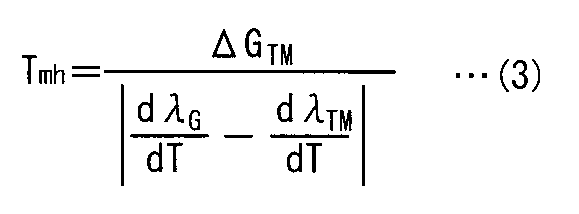
なお、式(3)のΔGTMは、上述のように式(2)の位相条件をみたす波長λTMの間隔(縦モード間隔)であるが、λTMが複数の値を取り得ることから、ΔGTMも複数の値を取り得る。また、dλG/dTは、上述のようにグレーティング反射率の反射率プロファイルにおける主ピークの波長λGの温度係数であり、dλTM/dTは、式(2)の位相条件をみたす出射光Bの波長λTMの温度係数である。
本実施の形態においては、上述のようにΔGTMの値を大きくすることに加えて、式(3)の右辺の分母|dλG/dT-dλTM/dT|が、以下に示す式(4)をみたすようにする。これにより、式(3)の温度Tmhの値が大きくなるので、モードホップの発生は抑制される。
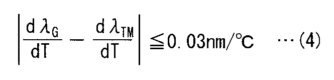
具体的には、屈折率の大きい材料は屈折率の温度変化が大きいという傾向を利用し、上述のように光学材料層11の屈折率nbを1.8以上とすることによって、温度係数dλG/dTの値を大きくすることで、式(4)をみたすようになっている。なお、式(4)の左辺の値は0.025以下であればさらに好ましい。
このように、外部共振器型発光装置1においてはモードホップの抑制もなされていることから、本実施の形態によれば、動作想定温度範囲内において環境温度が変化したとしても、波長変動および出力変動の抑制された外部共振器型発光装置1が実現されるといえる。
<第2の実施の形態>
上述した第1の実施の形態に係る外部共振器型発光装置1では、光学材料層11に一対のリッジ溝19を設けることによって、グレーティング素子9にリッジ型の光導波路18が設けられてなる。係る構成では、光導波路18以外の部分、具体的には、リッジ溝19の下方および側方にも光学材料層11が存在する。しかしながら、光導波路をリッジ型光導波路として設ける態様はこれに限られるものではない。本実施の形態では、光学材料層11を構成する材料と同じく屈折率nbが1.8以上である材料(以下、単に光学材料とも称する)からなるリッジ型の光導波路を、第1の実施の形態とは異なる態様にて具備するグレーティング素子について説明する。
上述した第1の実施の形態に係る外部共振器型発光装置1では、光学材料層11に一対のリッジ溝19を設けることによって、グレーティング素子9にリッジ型の光導波路18が設けられてなる。係る構成では、光導波路18以外の部分、具体的には、リッジ溝19の下方および側方にも光学材料層11が存在する。しかしながら、光導波路をリッジ型光導波路として設ける態様はこれに限られるものではない。本実施の形態では、光学材料層11を構成する材料と同じく屈折率nbが1.8以上である材料(以下、単に光学材料とも称する)からなるリッジ型の光導波路を、第1の実施の形態とは異なる態様にて具備するグレーティング素子について説明する。
図7は、本実施の形態に係る種々のグレーティング素子109(109A~109E)についてのYZ断面図である。図7(a)~(e)に示す5通りのグレーティング素子109A~109Eはいずれも、リッジ型の光導波路118が、光学材料からなりX軸方向に延在する細長いコアとなっており、該光導波路118のYZ断面(以下、横断面とも称する)が凸図形をなしている点で共通している。換言すれば、本実施の形態に係る種々のグレーティング素子109A~109Eにおいて光学材料にて構成されてなるのは、リッジ型光導波路118のみとなっている。
ここで、光導波路118のYZ断面が凸図形をなしているとは、光導波路118の横断面の外側輪郭線の任意の二点を結ぶ線分が、当該横断面の外側輪郭線の内側に位置することを意味する。このような凸図形としては、三角形、四角形、六角形、八角形などの多角形、円形、楕円形などを例示できる。なかでも、上辺と下辺と一対の側面を有する四角形が好ましく、台形が特に好ましい。
なお、図示は省略するが、グレーティング素子109の光導波路118においても、第1の実施の形態に係る外部共振器型発光装置1に備わるグレーティング素子9の光導波路18の場合と同様の態様にて、ブラッググレーティング12および伝搬部13が設けられてなる。加えて、光導波路118のX軸方向両端部には、グレーティング素子9に備わる無反射膜7B、7Cと同様の無反射膜が設けられてなる。そして、グレーティング素子109を用いて構成される外部共振器型発光装置は、第1の実施の形態に係る外部共振器型発光装置1のグレーティング素子9をグレーティング素子109にて置き換えたものとして構成される。すなわち、グレーティング素子109におけるレーザ光の発振に関する要件は全て、第1の実施の形態に係るグレーティング素子9における要件と同じである。
図7(a)に示すグレーティング素子109Aは、支持基板10上にバッファ層(第1のバッファ層)116を備え、該バッファ層116上に光導波路118(118A)を備えた構成を有する。光導波路118Aは、その横断面が上底よりも下底が長い台形形状をなすように設けられてなる。すなわち、光導波路118Aにおいては、バッファ層116と接する下側面よりも該下側面に対向する上側面の方が狭くなっている。係る光導波路118Aの幅Wmは1.5μm以上8μm以下であるのが好ましい。また、光導波路118Aの厚み(Z軸方向の高さ)Thは、0.5μm~3μmであるのが好ましい。なお、光導波路118Aの最大幅は0.7μm以上9μm以下であるのが好ましい。
第1のバッファ層116は、例えばSiO2、アルミナ、ポリイミド、エポキシ樹脂など、光学材料よりも屈折率の小さい材料から選択された材料にて0.2μm~2μm程度の厚みに形成されてなる。
係る構成を有するグレーティング素子109Aにおいては、バッファ層116と、光導波路118の周りに存在する空気(空気層)とが、コアたる光導波路118よりも相対的に屈折率の小さいクラッドとして機能する。
グレーティング素子109Aにおけるバッファ層116および光導波路118Aの形成は、スパッタ、真空蒸着、CVDなどの公知の薄膜形成手法によってバッファ層116と光導波路118Aを構成する光学材料からなる薄膜層とを順次に形成した後、後者の不要部分をエッチング除去することによって行える。なお、係るエッチングの際に併せてブラッググレーティング12を形成する態様であってもよい。
一方、図7(b)に示すグレーティング素子109Bは、図7(a)に示すグレーティング素子109Aに、光導波路118Aを上方および側方から覆うバッファ層(第2のバッファ層)117をさらに設けた構成を有する。第2のバッファ層117は、第1のバッファ層116と同様、例えばSiO2、アルミナ、ポリイミド、エポキシ樹脂などから選択された材料にて形成されてよいが、第1のバッファ層116とは異なる材料にて形成されてなる。また、第2のバッファ層117は、光導波路118の上方部分117bの厚みが0.2μm~2μm程度となるように形成される。
グレーティング素子109Bの形成は、グレーティング素子109Aを形成する場合と同様にバッファ層116および光導波路118Aを形成し、さらにはブラッググレーティング12を形成した後、スパッタ、真空蒸着、CVDなどの公知の薄膜形成手法によってバッファ層117を形成することによって行える。
また、図7(c)に示すグレーティング素子109Cは、横断面が上底よりも下底が短い台形形状をなすように設けられた光導波路118Bを備えるほかは、図7(b)に示すグレーティング素子109Bと同様の構成を有する。光導波路118Bにおいては、第1のバッファ層116と接する下側面が該下側面に対向する上側面よりも狭くなっている。係る光導波路118Bの配置態様は、換言すれば、光導波路118Aを上下反転させたものに相当する。
グレーティング素子109Cの形成は、光学材料からなる薄膜層をエッチングする際のエッチング条件を違えるほかは、グレーティング素子109Bの形成と同様に行える。
なお、図示は省略するが、グレーティング素子109が、係る光導波路118Bを備える一方で第2のバッファ層117を具備しない構成を有する態様であってもよい。これは、グレーティング素子109Aの光導波路118Aを上下反転させたものに相当する。
さらには、図7(d)および図7(e)に示すグレーティング素子109Dおよび109Eはそれぞれ、光導波路118Aもしくは118Bの周囲に一の材料からなるバッファ層122を設けた構成を有するものである。バッファ層122の第1のバッファ層116および第2のバッファ層117と同様、例えばSiO2、アルミナ、ポリイミド、エポキシ樹脂などから選択された材料にて形成されてよい。
これらグレーティング素子109Dおよび109Eの形成はそれぞれ、グレーティング素子109Bおよび109Cと同様の手順にて、第1のバッファ層116に相当する部分についてのバッファ層122の形成と、光導波路118Aもしくは118Bの形成さらにはブラッググレーティング12の形成とを行った後、引き続きバッファ層122の残りの部分を第2のバッファ層117と同様に形成することで行える。バッファ層122は、光導波路118の下方部分122aの厚みがグレーティング素子109A~109Cの第1のバッファ層116と同じ厚みとなるように、かつ、光導波路118の上方部分122bの厚みがグレーティング素子109A~109Cの第2のバッファ層117における光導波路118の上方部分117bと同じ厚みとなるように、形成される。
なお、図7(a)~(e)においてはバッファ層116、117、あるいは122が支持基板10の略全面を覆う態様にて形成される場合を例示しているが、これは必須の態様ではない。例えば、グレーティング素子109Aにおいては、少なくとも光導波路118Aの下方にバッファ層116が存在していれば、支持基板10が部分的に露出してなる態様であってもよい。同様に、グレーティング素子109B~109Eにおいては光導波路118Aあるいは118Bの周囲が覆われていれば、光導波路118の側方部分117cまたは122cが支持基板10の全てを覆うように設けられてなる必要はなく、支持基板10が部分的に露出してなる態様であってもよい。
また、本実施の形態に係るグレーティング素子109の場合も、第1の実施の形態に係るグレーティング素子9と同様、接着層15による貼り合わせによって形成することは可能である。例えば、グレーティング素子109Aを作製する場合であれば、光導波路118Aとなる光学材料からなる基板にあらかじめバッファ層116をスパッタ等で形成しておいたうえで、該バッファ層116と下地基板10とを接着層15にて貼り合わせ、その後、エッチングによって光導波路118を形成すればよい。グレーティング素子109B~109Eなど、光導波路118の上方にもバッファ層をさらに設ける場合は、係るエッチングおよびブラッググレーティング12の形成の後にこれを行えばよい。
以上のような構成を有するグレーティング素子109を備えた外部共振器型発光装置1においても、第1の実施の形態でのグレーティング素子9における反射波長の設定態様と同様の態様にてグレーティング素子109における反射波長を設定することによって、従来の装置において行われていたような、ペルチェ素子などを用いた温度制御を行うことなく、あるいはさらに、パワーモニター機能を備えることなく、波長安定動作およびパワー安定動作が実現される。
また、本実施の形態のように、コアたる光導波路118の部分のみを光学材料にて形成し、その周囲をクラッドとする構成を採用することは、第1の実施の形態の構成に比して、光閉じ込め効果が高まるという点や、光の伝搬損失低減、パッシベーションという点で好適である。
<変形例>
光学材料層11は、支持基板10上に薄膜層として形成してもよい。係る薄膜層の形成手法としては、スパッタ、蒸着、CVDを例示できる。この場合、光学材料層11は支持基板10に直接形成されるので、接着層15の形成は不要である。
光学材料層11は、支持基板10上に薄膜層として形成してもよい。係る薄膜層の形成手法としては、スパッタ、蒸着、CVDを例示できる。この場合、光学材料層11は支持基板10に直接形成されるので、接着層15の形成は不要である。
光源素子2およびグレーティング素子9の各端面は、端面反射を抑制する目的で斜めカットされていてもよい。
GaAs系半導体やInP系半導体のレーザのほか、上述の光源素子2に代えて一次元状に配列したレーザアレイ等の光源を使用することも可能である。あるいは、光源素子2として、スーパールミネッセンスダイオードや半導体光アンプ(SOA)を用いる態様であってもよい。
(実施例1)
図5に示すグレーティング素子9Aを作製し、その特性を評価した。
図5に示すグレーティング素子9Aを作製し、その特性を評価した。
具体的には、まず、グレーティング素子9Aを形成するために、光学材料層11の材料として屈折率nb=2.17であるy板MgOドープのニオブ酸リチウム結晶基板(以下、LN基板)を用意した。該結晶基板の一方主面上にマスクとして金属Ti膜を形成し、フォトリソグラフィー技術によるパターニングとフッ素系の反応性イオンエッチングとにより、ピッチΛ=225nm、長さLb=150μm、深さtd=15nmのブラッググレーティング12となるグレーティングパターンを形成した。なお、パターニングの際には、伝搬部13の長さLmが20μmとなるようにした。
続いて、エキシマレーザを用いて、グレーティングパターンの延在方向に沿ってリッジ溝19を形成することにより、幅Wm=3μm、深さTr=0.6μmの光導波路18を設けた。さらに、スパッタ装置によって、リッジ溝19が形成された側の面にSiO2からなる下側バッファ層16を0.5μmの厚みに形成した。その後、支持基板10としてブラックLN基板を用意し、その一方主面と下側バッファ層16とを接着して積層体を得た。接着層15はエポキシ系樹脂を使用して形成した。
次に、ブラックLN基板の非接着面側を研磨定盤に貼り付けて、露出しているLN基板の他方主面(ブラッググレーティングの非形成面)を精密研磨し、光学材料層11の厚みTsを1.2μmとした。その後、積層体を研磨定盤から外し、研磨面に対し、スパッタ装置によってSiO2からなる上側バッファ層17を0.5μmの厚みに形成した。
続いて、ダイシング装置にて、積層体をブラックグレーティングの延在方向が長手方向となる棒状に切断した。切断面を光学研磨した後、無反射膜7B、7Cとして反射率0.1%のARコートを形成した。最後に、チップ切断を行うことにより、グレーティング素子9Aを得た。最終的な素子サイズは長さLWG=500μm、幅=1mmとした。
得られたグレーティング素子9Aについて室温(20℃とする)での光学特性を評価した。具体的には、広帯域波長光源であるスーパ・ルミネッセンス・ダイオード(SLD)を使用して、グレーティング素子9AにTEモードの光を入力し、その出力光を光スペクトルアナライザで分析し、得られた透過特性から、グレーティング素子9Aの反射特性を評価した。
その結果、TEモードに対して、中心波長λG=991nm、最大反射率=10%、半値全幅△λG=0.5nmという結果を得た。
続いて、このグレーティング素子9Aを実装して、図1の外部共振器型発光装置1を作製した。
具体的には、光源素子2として、活性層5がGaAsからなり、反射膜6の反射率が97%で、反射膜20の反射率が3%であるGaAs系レーザを用意した。光源素子2の素子長(活性層5の長さ)Laは250μmであった。光源素子2から出射されるレーザ光(一次発光)の室温における中心波長は980nmであり、出力は60mWであった。
実装に際しては、共通基板3としてSUSを使用し、光源素子2とグレーティング素子9との間隔Lgは1μmとした。
実装後、ペルチェ素子による冷却を行うことなく、外部共振器型発光装置1Aを電流制御(ACC)で駆動したところ、室温においては、ブラッググレーティング12の反射プロファイルの中心波長λGに対応した波長990.9nmで発振する発振光(出射光B)が得られた。出力(レーザ出力)は、一次発光の出力よりも小さい40.1mWであった。
続いて、外部共振器型発光装置1Aを恒温槽内に設置し、30℃~70℃の温度範囲において10℃ごとに、一次発光の波長λ1と、発振光の波長λTMと、レーザ出力とを測定した。その結果を上述した室温(20℃)の結果も含めて表1に示す。なお、発振光の温度係数dλTM/dTは0.1nm/℃であり、式(4)はみたされていた。
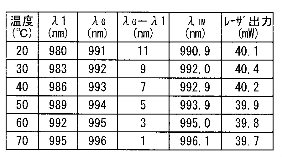
表1に示す結果からわかるように、本実施例においては、20℃~70℃の間における発振光(出射光B)のレーザ出力の差は最大で0.5mWであり、発振波長λTMの差は最大で5.2nmであった。
(実施例2)
ブラッググレーティング12を、ピッチΛ=222nm、長さLb=100μm、深さtd=40nmとなるように形成したほかは、実施例1と同様の手順でグレーティング素子9Aおよび外部共振器型発光装置1Aの作製および評価を行った。
ブラッググレーティング12を、ピッチΛ=222nm、長さLb=100μm、深さtd=40nmとなるように形成したほかは、実施例1と同様の手順でグレーティング素子9Aおよび外部共振器型発光装置1Aの作製および評価を行った。
ブラッググレーティング12の評価結果は、中心波長λG=991nm、最大反射率=20%、半値全幅△λG=2nmであった。
また、20℃~70℃での、外部共振器型発光装置1Aにおける一次発光の波長λ1と、発振光の波長λTMと、レーザ出力とを測定した結果を表2に示す。なお、発振光の温度係数dλTM/dTは0.1nm/℃であり、式(4)はみたされていた。
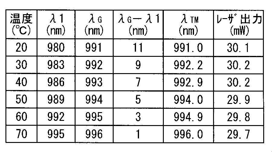
表2に示す結果からわかるように、本実施例においては、20℃~70℃の間における発振光(出射光B)のレーザ出力の差は最大で0.5mWであり、発振波長λTMの差は最大で5.0nmであった。
(実施例3)
本実施例では、光学材料層11を薄膜層として備えるグレーティング素子9を形成した。
本実施例では、光学材料層11を薄膜層として備えるグレーティング素子9を形成した。
具体的には、まず、支持基板10として石英基板を用意し、該石英基板の一方主面に対して、スパッタ装置にて光学材料層11としてのTa2O5層(屈折率nb=2.1)を1.2μmの厚みに形成した。次に、Ta2O5層の上にマスクとして金属Ni膜を形成し、フォトリソグラフィー技術によるパターニングとフッ素系の反応性イオンエッチングとにより、ピッチΛ=240nm、長さLb=100μm、深さtd=40nmのブラッググレーティング12となるグレーティングパターンを形成した。
次に、エキシマレーザにて、グレーティングパターンの延在方向に沿ってリッジ溝19を形成することにより、幅Wm=3μm、深さTr=0.6μmの光導波路18を設けた。
続いて、ダイシング装置にて、積層体をブラックグレーティングの延在方向が長手方向となる棒状に切断した。切断面を光学研磨した後、無反射膜7B、7Cとして反射率0.1%のARコートを形成した。最後に、チップ切断を行うことにより、グレーティング素子9を得た。最終的な素子サイズは長さLWG=500μm、幅=1mmとした。
以降のグレーティング素子9の評価、および、外部共振器型発光装置1の作製および評価は、実施例1と同様に行った。
ブラッググレーティング12の評価結果は、中心波長λG=993.5nm、最大反射率=20%、半値全幅△λG=2nmであった。
また、20℃~70℃での、外部共振器型発光装置1における一次発光の波長λ1と、発振光の波長λTMと、レーザ出力とを測定した結果を表3に示す。なお、発振光の温度係数dλTM/dTは0.05nm/℃であり、式(4)はみたされていた。
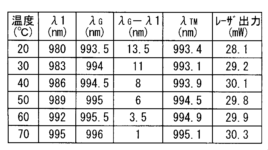
表2に示す結果からわかるように、本実施例においては、20℃~70℃の間における発振光(出射光B)のレーザ出力の差は最大で2.2mWであり、発振波長λTMの差は最大で2.1nmであった。
(比較例)
ブラッググレーティング12のピッチΛを222nmとしたほかは、実施例1と同様の手順でグレーティング素子9Aおよび外部共振器型発光装置1Aの作製および評価を行った。
ブラッググレーティング12のピッチΛを222nmとしたほかは、実施例1と同様の手順でグレーティング素子9Aおよび外部共振器型発光装置1Aの作製および評価を行った。
ブラッググレーティング12の評価結果は、中心波長λG=977nm、最大反射率=10%、半値全幅△λG=0.5nmであった。
また、20℃~70℃での、外部共振器型発光装置1Aにおける一次発光の波長λ1と、発振光の波長λTMと、レーザ出力とを測定した結果を表4に示す。なお、発振光の温度係数dλTM/dTは0.05nm/℃であり、式(4)はみたされていた。
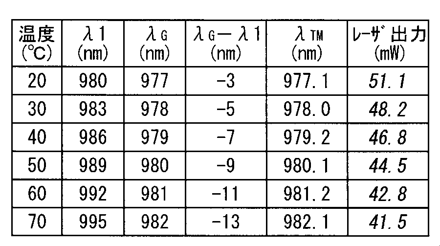
表4に示す結果からわかるように、本比較例においては、20℃~70℃の間における発振光(出射光B)のレーザ出力の差は最大で9.6mWであり、発振波長λTMの差は最大で5.0nmであった。
実施例1~実施例3の結果と本比較例の結果とを対比すると、前者の方が、レーザ出力の安定性に優れていることがわかる。
Claims (10)
- 外部共振器型発光装置であって、
レーザ光を発する活性層を有する半導体レーザ光源と、
前記活性層から発せられた前記レーザ光の光軸方向を長手方向とするリッジ型光導波路を備えるとともに、前記リッジ型光導波路の途中に設けられたブラッググレーティングを備えており、入射した前記レーザ光のうち所定の波長成分の光を前記半導体レーザ光源と前記ブラッググレーティングとの間で発振させて前記外部共振器型発光装置の外部への出射光として出射するグレーティング素子と、
を備え、
前記半導体レーザ光源から発せられる前記レーザ光の波長をλ1とし、
前記ブラッググレーティングの反射率プロファイルの中心波長をλGとし、前記反射率プロファイルの半値全幅をΔλGとするときに、
少なくとも-10℃以上30℃以下においてλ1<λG-ΔλG/2であるとともに、前記出射光の波長域がλG-ΔλG/2以上λG+ΔλG/2以下である、
ことを特徴とする外部共振器型発光装置。 - 請求項1に記載の外部共振器型発光装置であって、
50℃以下においてλG-λ1≧5nmであり、
20℃以下においてλG-λ1≧10nmである、
ことを特徴とする外部共振器型発光装置。 - 請求項1または請求項2に記載の外部共振器型発光装置であって、
前記グレーティング素子が、
支持基板と、
前記支持基板上に設けられてなり0.5μm以上3.0μm以下の厚みを有する光学材料層と、
前記支持基板と前記光学材料層とを接合する接合層と、
を備えており、
前記リッジ型光導波路が前記光学材料層に設けられており、
前記半導体レーザ光の光軸方向における前記ブラッググレーティングの長さをLbとし、前記ブラッググレーティングを構成する凹凸の深さをtdとするときに、
10μm≦Lb≦300μm
かつ
10nm≦td≦250nm
であることを特徴とする外部共振器型発光装置。 - 請求項3に記載の外部共振器型発光装置であって、
前記光学材料層の材質が、ガリウム砒素、ニオブ酸リチウム、酸化タンタル、酸化亜鉛および酸化アルミナからなる群より選択される、
ことを特徴とする外部共振器型発光装置。 - 請求項1または請求項2に記載の外部共振器型発光装置であって、
前記グレーティング素子が、支持基板の上に前記リッジ型光導波路を備える構成を有するものであり、
前記リッジ型光導波路が、前記長手方向に垂直な断面が凸図形をなすとともに0.5μm以上3.0μm以下の厚みを有してなり、
前記半導体レーザ光の光軸方向における前記ブラッググレーティングの長さをLbとし、前記ブラッググレーティングを構成する凹凸の深さをtdとするときに、
10μm≦Lb≦300μm
かつ
10nm≦td≦250nm
であることを特徴とする外部共振器型発光装置。 - 請求項5に記載の外部共振器型発光装置であって、
前記リッジ型光導波路の材質が、ガリウム砒素、ニオブ酸リチウム、酸化タンタル、酸化亜鉛および酸化アルミナからなる群より選択される、
ことを特徴とする外部共振器型発光装置。 - 請求項1ないし請求項6のいずれかに記載の外部共振器型発光装置であって、
前記半導体レーザ光の光軸方向における前記グレーティング素子の長さをLWGとするときに、
LWG≦500μm
であることを特徴とする外部共振器型発光装置。 - 請求項7に記載の外部共振器型発光装置であって、
0.5nm≦ΔλG≦3.0nm
であることを特徴とする外部共振器型発光装置。 - 請求項1ないし請求項8のいずれかに記載の外部共振器型発光装置であって、
前記波長域に、前記出射光の波長となる波長値が2以上5以下存在する、
ことを特徴とする外部共振器型発光装置。 - 請求項1ないし請求項9のいずれかに記載の外部共振器型発光装置であって、
ブラッグ波長の温度係数をdλG/dTとし、前記出射光の波長の温度係数をdλTM/dTとするときに、

Priority Applications (1)
| Application Number | Priority Date | Filing Date | Title |
|---|---|---|---|
| JP2015557920A JPWO2015108197A1 (ja) | 2014-01-20 | 2015-01-20 | 外部共振器型発光装置 |
Applications Claiming Priority (2)
| Application Number | Priority Date | Filing Date | Title |
|---|---|---|---|
| JP2014007597 | 2014-01-20 | ||
| JP2014-007597 | 2014-01-20 |
Publications (1)
| Publication Number | Publication Date |
|---|---|
| WO2015108197A1 true WO2015108197A1 (ja) | 2015-07-23 |
Family
ID=53543078
Family Applications (1)
| Application Number | Title | Priority Date | Filing Date |
|---|---|---|---|
| PCT/JP2015/051358 Ceased WO2015108197A1 (ja) | 2014-01-20 | 2015-01-20 | 外部共振器型発光装置 |
Country Status (2)
| Country | Link |
|---|---|
| JP (1) | JPWO2015108197A1 (ja) |
| WO (1) | WO2015108197A1 (ja) |
Cited By (1)
| Publication number | Priority date | Publication date | Assignee | Title |
|---|---|---|---|---|
| WO2017043222A1 (ja) * | 2015-09-08 | 2017-03-16 | 日本碍子株式会社 | 光学デバイス |
Citations (8)
| Publication number | Priority date | Publication date | Assignee | Title |
|---|---|---|---|---|
| JPH10303495A (ja) * | 1997-04-30 | 1998-11-13 | Fujitsu Ltd | 半導体レーザ |
| WO2000045482A1 (en) * | 1999-01-27 | 2000-08-03 | The Furukawa Electric Co., Ltd. | Semiconductor laser module |
| JP2002050827A (ja) * | 2000-08-01 | 2002-02-15 | Sumitomo Electric Ind Ltd | 半導体レーザ |
| US20070127538A1 (en) * | 2005-12-07 | 2007-06-07 | Electronics And Telecommunications Research Institute | Athermal external cavity laser |
| JP2008152003A (ja) * | 2006-12-18 | 2008-07-03 | Seiko Epson Corp | 光モジュール及び光通信装置 |
| US20120099611A1 (en) * | 2009-06-12 | 2012-04-26 | Mel | External cavity tunable laser module |
| WO2013034813A2 (en) * | 2011-09-07 | 2013-03-14 | Epicrystals Oy | Wavelength conversion unit |
| WO2014196553A1 (ja) * | 2013-06-07 | 2014-12-11 | 日本碍子株式会社 | 外部共振器型発光装置 |
-
2015
- 2015-01-20 JP JP2015557920A patent/JPWO2015108197A1/ja active Pending
- 2015-01-20 WO PCT/JP2015/051358 patent/WO2015108197A1/ja not_active Ceased
Patent Citations (8)
| Publication number | Priority date | Publication date | Assignee | Title |
|---|---|---|---|---|
| JPH10303495A (ja) * | 1997-04-30 | 1998-11-13 | Fujitsu Ltd | 半導体レーザ |
| WO2000045482A1 (en) * | 1999-01-27 | 2000-08-03 | The Furukawa Electric Co., Ltd. | Semiconductor laser module |
| JP2002050827A (ja) * | 2000-08-01 | 2002-02-15 | Sumitomo Electric Ind Ltd | 半導体レーザ |
| US20070127538A1 (en) * | 2005-12-07 | 2007-06-07 | Electronics And Telecommunications Research Institute | Athermal external cavity laser |
| JP2008152003A (ja) * | 2006-12-18 | 2008-07-03 | Seiko Epson Corp | 光モジュール及び光通信装置 |
| US20120099611A1 (en) * | 2009-06-12 | 2012-04-26 | Mel | External cavity tunable laser module |
| WO2013034813A2 (en) * | 2011-09-07 | 2013-03-14 | Epicrystals Oy | Wavelength conversion unit |
| WO2014196553A1 (ja) * | 2013-06-07 | 2014-12-11 | 日本碍子株式会社 | 外部共振器型発光装置 |
Cited By (1)
| Publication number | Priority date | Publication date | Assignee | Title |
|---|---|---|---|---|
| WO2017043222A1 (ja) * | 2015-09-08 | 2017-03-16 | 日本碍子株式会社 | 光学デバイス |
Also Published As
| Publication number | Publication date |
|---|---|
| JPWO2015108197A1 (ja) | 2017-03-23 |
Similar Documents
| Publication | Publication Date | Title |
|---|---|---|
| JP6125631B2 (ja) | 外部共振器型発光装置 | |
| JP5936771B2 (ja) | 外部共振器型発光装置 | |
| US20160372891A1 (en) | External resonator type light emitting device | |
| JP6554035B2 (ja) | グレーティング素子および外部共振器型発光装置 | |
| US9915794B2 (en) | Optical device, and optical-device production method | |
| JP5641631B1 (ja) | 外部共振器型発光装置 | |
| JP5936777B2 (ja) | グレーティング素子および外部共振器型発光装置 | |
| JP6629194B2 (ja) | 外部共振器型発光装置 | |
| JP2015115457A (ja) | 外部共振器型発光装置 | |
| JPWO2015108197A1 (ja) | 外部共振器型発光装置 | |
| WO2015190385A1 (ja) | 外部共振器型発光装置 | |
| WO2016093187A1 (ja) | 外部共振器型発光装置 | |
| JP2015039011A (ja) | 外部共振器型発光装置 | |
| WO2016152730A1 (ja) | 外部共振器型発光装置 | |
| JP2017126625A (ja) | 外部共振器型発光装置 | |
| WO2017043222A1 (ja) | 光学デバイス | |
| WO2015087914A1 (ja) | 外部共振器型発光装置 | |
| JP2015103732A (ja) | グレーティング素子および外部共振器型発光装置 | |
| WO2016125746A1 (ja) | 光導波路素子および光学デバイス |
Legal Events
| Date | Code | Title | Description |
|---|---|---|---|
| 121 | Ep: the epo has been informed by wipo that ep was designated in this application |
Ref document number: 15737535 Country of ref document: EP Kind code of ref document: A1 |
|
| ENP | Entry into the national phase |
Ref document number: 2015557920 Country of ref document: JP Kind code of ref document: A |
|
| NENP | Non-entry into the national phase |
Ref country code: DE |
|
| 122 | Ep: pct application non-entry in european phase |
Ref document number: 15737535 Country of ref document: EP Kind code of ref document: A1 |