WO2015107715A1 - 実装基板の製造装置、及び実装基板の製造方法 - Google Patents
実装基板の製造装置、及び実装基板の製造方法 Download PDFInfo
- Publication number
- WO2015107715A1 WO2015107715A1 PCT/JP2014/072396 JP2014072396W WO2015107715A1 WO 2015107715 A1 WO2015107715 A1 WO 2015107715A1 JP 2014072396 W JP2014072396 W JP 2014072396W WO 2015107715 A1 WO2015107715 A1 WO 2015107715A1
- Authority
- WO
- WIPO (PCT)
- Prior art keywords
- substrate
- mounting
- receiving portion
- driver
- substrate receiving
- Prior art date
- Legal status (The legal status is an assumption and is not a legal conclusion. Google has not performed a legal analysis and makes no representation as to the accuracy of the status listed.)
- Ceased
Links
Images













Classifications
-
- H—ELECTRICITY
- H10—SEMICONDUCTOR DEVICES; ELECTRIC SOLID-STATE DEVICES NOT OTHERWISE PROVIDED FOR
- H10W—GENERIC PACKAGES, INTERCONNECTIONS, CONNECTORS OR OTHER CONSTRUCTIONAL DETAILS OF DEVICES COVERED BY CLASS H10
- H10W72/00—Interconnections or connectors in packages
- H10W72/071—Connecting or disconnecting
- H10W72/073—Connecting or disconnecting of die-attach connectors
-
- G—PHYSICS
- G02—OPTICS
- G02F—OPTICAL DEVICES OR ARRANGEMENTS FOR THE CONTROL OF LIGHT BY MODIFICATION OF THE OPTICAL PROPERTIES OF THE MEDIA OF THE ELEMENTS INVOLVED THEREIN; NON-LINEAR OPTICS; FREQUENCY-CHANGING OF LIGHT; OPTICAL LOGIC ELEMENTS; OPTICAL ANALOGUE/DIGITAL CONVERTERS
- G02F1/00—Devices or arrangements for the control of the intensity, colour, phase, polarisation or direction of light arriving from an independent light source, e.g. switching, gating or modulating; Non-linear optics
- G02F1/01—Devices or arrangements for the control of the intensity, colour, phase, polarisation or direction of light arriving from an independent light source, e.g. switching, gating or modulating; Non-linear optics for the control of the intensity, phase, polarisation or colour
- G02F1/13—Devices or arrangements for the control of the intensity, colour, phase, polarisation or direction of light arriving from an independent light source, e.g. switching, gating or modulating; Non-linear optics for the control of the intensity, phase, polarisation or colour based on liquid crystals, e.g. single liquid crystal display cells
- G02F1/1303—Apparatus specially adapted to the manufacture of LCDs
-
- H—ELECTRICITY
- H10—SEMICONDUCTOR DEVICES; ELECTRIC SOLID-STATE DEVICES NOT OTHERWISE PROVIDED FOR
- H10W—GENERIC PACKAGES, INTERCONNECTIONS, CONNECTORS OR OTHER CONSTRUCTIONAL DETAILS OF DEVICES COVERED BY CLASS H10
- H10W72/00—Interconnections or connectors in packages
- H10W72/01—Manufacture or treatment
- H10W72/013—Manufacture or treatment of die-attach connectors
- H10W72/01321—Manufacture or treatment of die-attach connectors using local deposition
- H10W72/01325—Manufacture or treatment of die-attach connectors using local deposition in solid form
-
- H—ELECTRICITY
- H10—SEMICONDUCTOR DEVICES; ELECTRIC SOLID-STATE DEVICES NOT OTHERWISE PROVIDED FOR
- H10W—GENERIC PACKAGES, INTERCONNECTIONS, CONNECTORS OR OTHER CONSTRUCTIONAL DETAILS OF DEVICES COVERED BY CLASS H10
- H10W72/00—Interconnections or connectors in packages
- H10W72/071—Connecting or disconnecting
- H10W72/0711—Apparatus therefor
- H10W72/07141—Means for applying energy, e.g. ovens or lasers
-
- H—ELECTRICITY
- H10—SEMICONDUCTOR DEVICES; ELECTRIC SOLID-STATE DEVICES NOT OTHERWISE PROVIDED FOR
- H10W—GENERIC PACKAGES, INTERCONNECTIONS, CONNECTORS OR OTHER CONSTRUCTIONAL DETAILS OF DEVICES COVERED BY CLASS H10
- H10W72/00—Interconnections or connectors in packages
- H10W72/071—Connecting or disconnecting
- H10W72/0711—Apparatus therefor
- H10W72/07173—Means for moving chips, wafers or other parts, e.g. conveyor belts
-
- H—ELECTRICITY
- H10—SEMICONDUCTOR DEVICES; ELECTRIC SOLID-STATE DEVICES NOT OTHERWISE PROVIDED FOR
- H10W—GENERIC PACKAGES, INTERCONNECTIONS, CONNECTORS OR OTHER CONSTRUCTIONAL DETAILS OF DEVICES COVERED BY CLASS H10
- H10W72/00—Interconnections or connectors in packages
- H10W72/071—Connecting or disconnecting
- H10W72/0711—Apparatus therefor
- H10W72/07178—Means for aligning
-
- H—ELECTRICITY
- H10—SEMICONDUCTOR DEVICES; ELECTRIC SOLID-STATE DEVICES NOT OTHERWISE PROVIDED FOR
- H10W—GENERIC PACKAGES, INTERCONNECTIONS, CONNECTORS OR OTHER CONSTRUCTIONAL DETAILS OF DEVICES COVERED BY CLASS H10
- H10W72/00—Interconnections or connectors in packages
- H10W72/071—Connecting or disconnecting
- H10W72/0711—Apparatus therefor
- H10W72/07183—Means for monitoring
-
- H—ELECTRICITY
- H10—SEMICONDUCTOR DEVICES; ELECTRIC SOLID-STATE DEVICES NOT OTHERWISE PROVIDED FOR
- H10W—GENERIC PACKAGES, INTERCONNECTIONS, CONNECTORS OR OTHER CONSTRUCTIONAL DETAILS OF DEVICES COVERED BY CLASS H10
- H10W72/00—Interconnections or connectors in packages
- H10W72/071—Connecting or disconnecting
- H10W72/0711—Apparatus therefor
- H10W72/07188—Apparatus chuck
-
- H—ELECTRICITY
- H10—SEMICONDUCTOR DEVICES; ELECTRIC SOLID-STATE DEVICES NOT OTHERWISE PROVIDED FOR
- H10W—GENERIC PACKAGES, INTERCONNECTIONS, CONNECTORS OR OTHER CONSTRUCTIONAL DETAILS OF DEVICES COVERED BY CLASS H10
- H10W72/00—Interconnections or connectors in packages
- H10W72/071—Connecting or disconnecting
- H10W72/072—Connecting or disconnecting of bump connectors
-
- H—ELECTRICITY
- H10—SEMICONDUCTOR DEVICES; ELECTRIC SOLID-STATE DEVICES NOT OTHERWISE PROVIDED FOR
- H10W—GENERIC PACKAGES, INTERCONNECTIONS, CONNECTORS OR OTHER CONSTRUCTIONAL DETAILS OF DEVICES COVERED BY CLASS H10
- H10W72/00—Interconnections or connectors in packages
- H10W72/071—Connecting or disconnecting
- H10W72/073—Connecting or disconnecting of die-attach connectors
- H10W72/07331—Connecting techniques
- H10W72/07332—Compression bonding, e.g. thermocompression bonding
-
- H—ELECTRICITY
- H10—SEMICONDUCTOR DEVICES; ELECTRIC SOLID-STATE DEVICES NOT OTHERWISE PROVIDED FOR
- H10W—GENERIC PACKAGES, INTERCONNECTIONS, CONNECTORS OR OTHER CONSTRUCTIONAL DETAILS OF DEVICES COVERED BY CLASS H10
- H10W72/00—Interconnections or connectors in packages
- H10W72/071—Connecting or disconnecting
- H10W72/073—Connecting or disconnecting of die-attach connectors
- H10W72/07331—Connecting techniques
- H10W72/07337—Connecting techniques using a polymer adhesive, e.g. an adhesive based on silicone or epoxy
- H10W72/07338—Connecting techniques using a polymer adhesive, e.g. an adhesive based on silicone or epoxy hardening the adhesive by curing, e.g. thermosetting
-
- H—ELECTRICITY
- H10—SEMICONDUCTOR DEVICES; ELECTRIC SOLID-STATE DEVICES NOT OTHERWISE PROVIDED FOR
- H10W—GENERIC PACKAGES, INTERCONNECTIONS, CONNECTORS OR OTHER CONSTRUCTIONAL DETAILS OF DEVICES COVERED BY CLASS H10
- H10W72/00—Interconnections or connectors in packages
- H10W72/071—Connecting or disconnecting
- H10W72/074—Connecting or disconnecting of anisotropic conductive adhesives
-
- H—ELECTRICITY
- H10—SEMICONDUCTOR DEVICES; ELECTRIC SOLID-STATE DEVICES NOT OTHERWISE PROVIDED FOR
- H10W—GENERIC PACKAGES, INTERCONNECTIONS, CONNECTORS OR OTHER CONSTRUCTIONAL DETAILS OF DEVICES COVERED BY CLASS H10
- H10W72/00—Interconnections or connectors in packages
- H10W72/20—Bump connectors, e.g. solder bumps or copper pillars; Dummy bumps; Thermal bumps
- H10W72/241—Dispositions, e.g. layouts
-
- H—ELECTRICITY
- H10—SEMICONDUCTOR DEVICES; ELECTRIC SOLID-STATE DEVICES NOT OTHERWISE PROVIDED FOR
- H10W—GENERIC PACKAGES, INTERCONNECTIONS, CONNECTORS OR OTHER CONSTRUCTIONAL DETAILS OF DEVICES COVERED BY CLASS H10
- H10W72/00—Interconnections or connectors in packages
- H10W72/20—Bump connectors, e.g. solder bumps or copper pillars; Dummy bumps; Thermal bumps
- H10W72/241—Dispositions, e.g. layouts
- H10W72/247—Dispositions of multiple bumps
- H10W72/248—Top-view layouts, e.g. mirror arrays
-
- H—ELECTRICITY
- H10—SEMICONDUCTOR DEVICES; ELECTRIC SOLID-STATE DEVICES NOT OTHERWISE PROVIDED FOR
- H10W—GENERIC PACKAGES, INTERCONNECTIONS, CONNECTORS OR OTHER CONSTRUCTIONAL DETAILS OF DEVICES COVERED BY CLASS H10
- H10W72/00—Interconnections or connectors in packages
- H10W72/20—Bump connectors, e.g. solder bumps or copper pillars; Dummy bumps; Thermal bumps
- H10W72/251—Materials
- H10W72/252—Materials comprising solid metals or solid metalloids, e.g. PbSn, Ag or Cu
-
- H—ELECTRICITY
- H10—SEMICONDUCTOR DEVICES; ELECTRIC SOLID-STATE DEVICES NOT OTHERWISE PROVIDED FOR
- H10W—GENERIC PACKAGES, INTERCONNECTIONS, CONNECTORS OR OTHER CONSTRUCTIONAL DETAILS OF DEVICES COVERED BY CLASS H10
- H10W72/00—Interconnections or connectors in packages
- H10W72/20—Bump connectors, e.g. solder bumps or copper pillars; Dummy bumps; Thermal bumps
- H10W72/261—Functions other than electrical connecting
-
- H—ELECTRICITY
- H10—SEMICONDUCTOR DEVICES; ELECTRIC SOLID-STATE DEVICES NOT OTHERWISE PROVIDED FOR
- H10W—GENERIC PACKAGES, INTERCONNECTIONS, CONNECTORS OR OTHER CONSTRUCTIONAL DETAILS OF DEVICES COVERED BY CLASS H10
- H10W74/00—Encapsulations, e.g. protective coatings
- H10W74/10—Encapsulations, e.g. protective coatings characterised by their shape or disposition
- H10W74/15—Encapsulations, e.g. protective coatings characterised by their shape or disposition on active surfaces of flip-chip devices, e.g. underfills
-
- H—ELECTRICITY
- H10—SEMICONDUCTOR DEVICES; ELECTRIC SOLID-STATE DEVICES NOT OTHERWISE PROVIDED FOR
- H10W—GENERIC PACKAGES, INTERCONNECTIONS, CONNECTORS OR OTHER CONSTRUCTIONAL DETAILS OF DEVICES COVERED BY CLASS H10
- H10W90/00—Package configurations
- H10W90/701—Package configurations characterised by the relative positions of pads or connectors relative to package parts
- H10W90/721—Package configurations characterised by the relative positions of pads or connectors relative to package parts of bump connectors
- H10W90/724—Package configurations characterised by the relative positions of pads or connectors relative to package parts of bump connectors between a chip and a stacked insulating package substrate, interposer or RDL
-
- H—ELECTRICITY
- H10—SEMICONDUCTOR DEVICES; ELECTRIC SOLID-STATE DEVICES NOT OTHERWISE PROVIDED FOR
- H10W—GENERIC PACKAGES, INTERCONNECTIONS, CONNECTORS OR OTHER CONSTRUCTIONAL DETAILS OF DEVICES COVERED BY CLASS H10
- H10W90/00—Package configurations
- H10W90/701—Package configurations characterised by the relative positions of pads or connectors relative to package parts
- H10W90/731—Package configurations characterised by the relative positions of pads or connectors relative to package parts of die-attach connectors
- H10W90/734—Package configurations characterised by the relative positions of pads or connectors relative to package parts of die-attach connectors between a chip and a stacked insulating package substrate, interposer or RDL
Definitions
- the present invention relates to a mounting board manufacturing apparatus and a mounting board manufacturing method.
- Display devices equipped with a display panel such as a liquid crystal panel are used for portable electronic devices such as mobile phones, smartphones, and notebook computers.
- a display device includes a display panel having a display unit for displaying an image, and a semiconductor that drives the display panel by supplying an output signal generated by processing an input signal supplied from a signal supply source to the display unit.
- a chip As described above, in a display device that is generally classified into small and medium size, as a semiconductor chip mounting method, a COG (Chip On Glass) mounting technique in which a semiconductor chip is directly mounted in an area outside the display portion of the display panel. Is preferably used.
- COG Chip On Glass
- Patent Document 1 described above describes a manufacturing apparatus in which a guide plate having a rough surface with an upper surface of 0.1 ⁇ m to 5 ⁇ m is arranged on a part of the upper surface of a mounting table on which a substrate constituting a display panel is mounted. Yes. In this way, the contact area between the bottom surface of the substrate and the guide plate is reduced, so that heat from the head disposed on the side opposite to the mounting table side with respect to the substrate becomes difficult to be transmitted to the guide plate.
- a semiconductor chip can be mounted in a short time.
- the present invention has been completed based on the above situation, and an object thereof is to suppress the occurrence of mounting defects.
- a mounting substrate manufacturing apparatus includes a substrate receiving portion that receives a substrate, and a mounting component that is disposed on the opposite side of the substrate receiving portion from the substrate and is interposed between the substrate and the substrate.
- the substrate receiving portion was supported from the opposite side to the substrate side, and the substrate receiving portion was inclined on the substrate receiving portion side plate surface of the substrate. And a tilting support section that tilts to follow the tilt in some cases.
- the mounting component can be mounted on the substrate by pressing the mounting component against the substrate from the side opposite to the substrate receiving portion side with the pressing portion while receiving the substrate by the substrate receiving portion.
- the shape of the plate surface on the substrate receiving portion side of the substrate is not flat, for example, it is an inclined shape
- the substrate receiving portion follows the inclination on the plate surface of the substrate by the tilting support portion. Therefore, the mounting component is pressed by the pressing unit in a state where the substrate is firmly received by the substrate receiving unit.
- unevenness is hardly generated in the pressure applied to the mounting component from the pressurizing portion, so that mounting failure is unlikely to occur.
- the board receiving portion is configured to selectively receive a component mounting portion on which the mounting component is mounted among the boards, and is disposed on the same side as the board receiving portion with respect to the board.
- a board holding unit that holds the main board part of the board excluding the component mounting part is provided. In this way, by holding the board main part of the board by the board holding part, it is possible to fix the arrangement of the entire board including the component mounting part. It can pressurize more stably by a pressurizing part. As a result, unevenness is less likely to occur due to the pressure applied to the mounting component from the pressurizing portion, and therefore, mounting defects are less likely to occur.
- the tilt support portion is configured to support the substrate receiving portion so that the substrate receiving portion can be relatively displaced, and a support surface supporting the substrate receiving portion is formed of a curved surface. In this way, when the substrate receiving portion is supported so as to be relatively displaceable by the curved support surface of the tilt support portion, the plate surface on the substrate receiving portion side of the substrate is inclined. It is tilted appropriately following the tilt. If the tilt support part is integrated with the substrate receiving part, the structure becomes simple as compared to the case where a member that supports the tilt support part so as to be relatively displaceable is required.
- the tilting support portion is configured such that the support surface is a spherical surface. In this way, since the degree of freedom of tilting of the substrate receiving portion is high, if the plate surface on the substrate receiving portion side of the substrate is inclined, the substrate receiving portion is more suitable following the inclination. Can be tilted. As a result, unevenness is less likely to occur in the pressure applied to the mounting component from the pressurizing portion, so that mounting defects are less likely to occur.
- a posture holding portion that supports the substrate receiving portion from a side opposite to the substrate side and holds the posture of the substrate receiving portion. In this way, when the substrate receiving part is relatively displaced with respect to the tilting support part with the tilting, the posture holding part supports the substrate receiving part from the side opposite to the substrate side. Can be held appropriately. As a result, unevenness is less likely to occur in the pressure applied to the mounting component from the pressurizing portion, so that mounting defects are less likely to occur.
- the mounting components have a longitudinal shape, and at least a pair of the posture holding portions are arranged so as to sandwich the tilt support portion from both sides in the longitudinal direction of the mounting components.
- the shape of the board surface on the substrate receiving portion side of the substrate is inclined with respect to the longitudinal direction of the mounting component having a longitudinal shape, uneven pressure tends to occur more easily in the mounting component in the longitudinal direction.
- the posture holding parts are arranged at least in a pair so as to sandwich the tilting support part from both sides in the longitudinal direction of the mounted component, the board holding part is relative to the tilting support part as the board receiving part tilts in the longitudinal direction.
- the substrate receiving portion When displaced, the substrate receiving portion is supported from the side opposite to the substrate side by at least one pair of posture holding portions, so that the posture of the substrate receiving portion can be more appropriately held.
- the posture of the substrate receiving portion can be more appropriately held.
- the tilt support portion is configured such that the support surface is a spherical surface, and at least three of the posture holding portions are arranged at equiangular intervals when viewed in plan with the tilt support portion as a center. Has been.
- the support surface of the tilt support portion is a spherical surface
- the substrate receiving portion to be supported has a high degree of freedom in tilting, so that the substrate surface on the substrate receiving portion side is inclined. In such a case, the substrate receiving portion can be more suitably tilted following the tilt.
- the posture of the substrate receiving portion tilted with a high degree of tilt freedom is more appropriate. Can be held in. As a result, unevenness is less likely to occur in the pressure applied to the mounting component from the pressurizing portion, so that mounting defects are less likely to occur.
- the posture holding unit includes an elastic support unit that elastically supports the substrate receiving unit from the side opposite to the substrate side. If it does in this way, the attitude
- the elastic support portion is elastically restored, so that the posture of the board receiving portion can be restored.
- the posture holding unit is made of a damper. If it does in this way, a substrate receiving part can be stably held by supporting a substrate receiving part from the opposite side to a substrate side with a damper.
- the posture holding unit is an air cylinder. If it does in this way, a substrate receiving part can be stably held by supporting a substrate receiving part from the opposite side to a substrate side with an air cylinder.
- the tilt support portion is fixed to the substrate receiving portion, and a receiving portion fixing portion whose surface opposite to the substrate receiving portion side is curved, and the receiving portion fixing portion is relatively displaceable. And a fixing portion supporting portion that supports the receiving portion fixing portion from a side opposite to the substrate receiving portion side in contact with the curved surface.
- the receiving portion fixing portion fixed to the substrate receiving portion can be relatively displaced by being supported from the opposite side of the substrate receiving portion side by the fixing portion supporting portion in contact with the curved surface.
- the fixing portion support portion has a curved surface in which the surface on the receiving portion fixing portion side follows the curved surface, and the curved surface of the receiving portion fixing portion so as to maintain the posture of the receiving portion fixing portion.
- a vacuum posture holding unit that vacuums a space between the fixed portion support portion and the curved surface is provided. In this way, the space between the curved surface of the receiving portion fixing portion and the curved surface of the fixing portion supporting portion is evacuated by the vacuum posture holding portion in a state where the receiving portion fixing portion is tilted together with the substrate receiving portion. By doing so, the posture of the receiving portion fixing portion can be suitably held. After mounting the mounting parts, return the posture of the receiving part fixing part to its original position by releasing the vacuum state of the space between the curved surface of the receiving part fixing part and the curved surface of the fixing part support part. Can do.
- the mounting substrate manufacturing method of the present invention includes a substrate thinning step for thinning the substrate by subjecting the substrate to a thickness opposite to the mounting plate surface on which the mounting component is mounted.
- the substrate receiving portion is supported by the substrate receiving portion from the side opposite to the mounting component side, and the substrate receiving portion is adapted to follow the inclination of the opposite plate surface when the opposite plate surface of the substrate is inclined.
- a mounting step in which the mounting component is pressed by a pressing portion disposed on the side opposite to the substrate side with respect to the mounting component while being tilted by the tilt support portion.
- the substrate is thinned by applying a thinning process to the opposite plate surface of the substrate opposite to the mounting plate surface on which the mounting component is mounted.
- the substrate is supported by the substrate receiving portion from the side opposite to the mounting component side, and the substrate receiving portion is tilted by the tilt supporting portion so as to follow the inclination of the opposite plate surface of the substrate. Therefore, unevenness is less likely to occur in the pressure applied to the mounting component when the mounting component is pressed by the pressurizing unit disposed on the side opposite to the substrate side with respect to the mounting component. Accordingly, it is difficult to cause mounting defects.
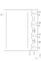
- FIG. 1 is a schematic plan view showing a connection configuration of a liquid crystal panel, a flexible substrate, and a control circuit board on which a driver according to Embodiment 1 of the present invention is mounted.
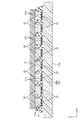
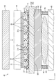
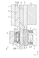
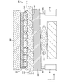
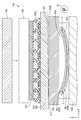
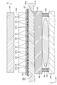
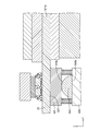
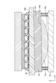
- Schematic sectional view showing the sectional structure of the liquid crystal panel The enlarged plan view which shows the mounting area of the driver and flexible substrate in the array substrate which comprises a liquid crystal panel AA line sectional view of FIG. BB sectional view of FIG. 4 is a cross-sectional view taken along the line AA of FIG. 4 showing the operation of the pressing unit of the driver mounting apparatus when the outer plate surface of the glass substrate forming the array substrate is not inclined.
- 4 is a cross-sectional view taken along the line BB of FIG. 4 showing the operation of the pressing unit of the driver mounting device when the outside plate surface of the glass substrate forming the array substrate is not inclined.
- 4 is a cross-sectional view taken along the line AA in FIG. 4 showing a state in which the driver is mounted by the pressurizing unit of the driver mounting apparatus when there is no inclination on the outer surface of the glass substrate forming the array substrate.
- 4 is a cross-sectional view taken along the line BB of FIG. 4 showing a state in which the driver is mounted by the pressure unit of the driver mounting apparatus when the outer plate surface of the glass substrate forming the array substrate is not inclined.
- 4 is a cross-sectional view taken along the line BB in FIG.
- 4 showing the operation of the pressing unit of the driver mounting device when the outer surface of the glass substrate forming the array substrate is inclined in the X-axis direction.
- 4 is a cross-sectional view taken along the line BB of FIG. 4 showing a state in which the driver is mounted by the pressurizing unit of the driver mounting device when the outer surface of the glass substrate forming the array substrate is inclined in the X-axis direction.
- 4 is a cross-sectional view taken along the line AA in FIG. 4 showing the operation of the pressing unit of the driver mounting device when the outer surface of the glass substrate forming the array substrate is inclined in the Y-axis direction.
- 4 is a cross-sectional view taken along line AA in FIG.
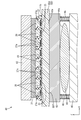
- Sectional drawing which shows the cross-sectional structure about the X-axis direction showing operation
- Sectional drawing which shows the cross-sectional structure about the X-axis direction in the state in which the driver was mounted by the pressurization part of the driver mounting apparatus
- Sectional drawing which shows the cross-sectional structure about the X-axis direction showing operation
- Sectional drawing which shows the cross-sectional structure about the X-axis direction in the state in which the driver was mounted by the pressurization part of the driver mounting apparatus
- Sectional drawing which shows the cross-sectional structure about the X-axis direction showing operation
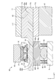
- movement of the pressurization part of the driver mounting apparatus which concerns on Embodiment 4 of this invention.
- Sectional drawing which shows the cross-sectional structure about the X-axis direction in the state in which the driver was mounted by the pressurization part of the driver mounting apparatus
- Sectional drawing which shows the cross-sectional structure about the Y-axis direction showing operation
- Sectional drawing which shows the cross-sectional structure about the Y-axis direction in the state in which the driver was mounted by the pressurization part of the driver mounting apparatus
- Sectional drawing which shows the cross-sectional structure about the X-axis direction showing operation
- Sectional drawing which shows the cross-sectional structure about the X-axis direction in the state in which the flexible substrate was mounted in the liquid crystal panel by the pressurization part of the flexible substrate mounting apparatus
- the top view which shows the plane structure of the liquid crystal panel which concerns on Embodiment 6 of this invention, a flexible substrate, and a printed circuit board.
- FIG. 25 is a cross-sectional view taken along the line CC of FIG. Sectional drawing which shows the cross-sectional structure about the X-axis direction in the state in which the driver was mounted by the pressurization part of the driver mounting apparatus which concerns on Embodiment 7 of this invention.
- Sectional drawing which shows the cross-sectional structure about the Y-axis direction in the state in which the driver was mounted by the pressurization part of the driver mounting apparatus
- Sectional drawing which shows the cross-sectional structure about the X-axis direction in the state in which the driver was mounted by the pressurization part of the driver mounting apparatus which concerns on Embodiment 8 of this invention.
- Sectional drawing which shows the cross-sectional structure about the Y-axis direction in the state in which the driver was mounted by the pressurization part of the driver mounting apparatus which concerns on Embodiment 9 of this invention.
- FIGS. 1 A first embodiment of the present invention will be described with reference to FIGS.
- a method for manufacturing a liquid crystal panel (display panel) 11 constituting the liquid crystal display device 10 and a driver mounting device (manufacturing device) 40 used for the manufacture will be exemplified.
- a part of each drawing shows an X axis, a Y axis, and a Z axis, and each axis direction is drawn to be a direction shown in each drawing. 2 and 3, the upper side of the figure is the front side and the lower side of the figure is the back side.
- the liquid crystal display device 10 includes a liquid crystal panel 11, a driver (mounted component) 21 that is mounted on the liquid crystal panel 11 and drives the liquid crystal panel 11, and various input signals to the driver 21.
- a backlight device (illumination device) 14 that is an external light source for supplying light.
- the liquid crystal display device 10 also includes a pair of front and back exterior members 15 and 16 for housing and holding the liquid crystal panel 11 and the backlight device 14 assembled to each other.
- the liquid crystal display device 10 includes a portable information terminal (including an electronic book and a PDA), a mobile phone (including a smartphone), a notebook computer (including a tablet notebook computer), a digital photo frame, It is used for various electronic devices (not shown) such as portable game machines and electronic ink paper. For this reason, the screen size of the liquid crystal panel 11 constituting the liquid crystal display device 10 is set to about several inches to several tens of inches, and is generally classified into a small size and a small size.
- the backlight device 14 includes a chassis 14a having a substantially box shape that opens toward the front side (the liquid crystal panel 11 side), and a light source (not shown) disposed in the chassis 14a (for example, a cold cathode tube, LED, organic EL, etc.) and an optical member (not shown) arranged to cover the opening of the chassis 14a.
- the optical member has a function of converting light emitted from the light source into a planar shape.
- the liquid crystal panel 11 has a vertically long rectangular shape (rectangular shape) as a whole, and an image is located at a position offset toward one end side (upper side in FIG. 1) in the long side direction.
- Display area (active area) AA is arranged, and the driver 21 and the flexible substrate 13 are respectively attached to the other end side in the long side direction (the lower side shown in FIG. 1).
- an area outside the display area AA is a non-display area (non-active area) NAA in which no image is displayed, and a part of the non-display area NAA is a mounting area for the driver 21 and the flexible substrate 13. Yes.
- a frame-shaped one-dot chain line that is slightly smaller than the CF substrate 11a represents the outer shape of the display area AA, and an area outside the one-dot chain line is a non-display area NAA.
- the liquid crystal panel 11 is interposed between a pair of transparent (excellent light-transmitting) substrates 11a and 11b and both the substrates 11a and 11b, and its optical characteristics change as an electric field is applied.
- a liquid crystal layer 11c containing liquid crystal molecules as a substance, and both substrates 11a and 11b are bonded together by a sealing agent (not shown) while maintaining a cell gap corresponding to the thickness of the liquid crystal layer 11c.
- Both the substrates 11a and 11b are each provided with a glass substrate GS made of alkali-free glass, quartz glass or the like, and a plurality of films are laminated on each glass substrate GS by a known photolithography method or the like. .
- the front side is a CF substrate (counter substrate) 11a
- the back side is an array substrate (mounting substrate, element substrate, active matrix substrate) 11b
- the CF substrate 11a has a short side dimension substantially equal to that of the array substrate 11b as shown in FIGS. 1 and 2, but the long side dimension is smaller than that of the array substrate 11b. It is bonded to 11b with one end (upper side shown in FIG. 1) in the long side direction aligned. Therefore, the other end (the lower side shown in FIG.
- the configuration existing in the display area AA in the array substrate 11b and the CF substrate 11a will be briefly described.
- the TFTs 17 and the pixel electrodes 18 are provided side by side in a matrix, and are arranged around the TFTs 17 and the pixel electrodes 18 so as to surround a gate wiring and a source wiring (both not shown).
- the TFT 17 and the pixel electrode 18 are arranged in parallel in a matrix form at the intersection of the gate wiring and the source wiring forming a lattice shape.
- the gate wiring and the source wiring are connected to the gate electrode and the source electrode of the TFT 17, respectively, and the pixel electrode 18 is connected to the drain electrode of the TFT 17.
- the pixel electrode 18 has a vertically long rectangular shape (rectangular shape) when seen in a plan view, and is made of a transparent electrode material such as ITO (IndiumInTin Oxide) or ZnO (Zinc Oxide).
- the array substrate 11b can be provided with a capacitor wiring (not shown) that is parallel to the gate wiring and that crosses the pixel electrode 18.
- the CF substrate 11a has colored portions such as R (red), G (green), and B (blue) as viewed in plan with the pixel electrodes 18 on the array substrate 11b side.
- a large number of color filters 11h are arranged in parallel so as to overlap each other.
- a substantially lattice-shaped light shielding layer (black matrix) 11i for preventing color mixture is formed between each colored portion constituting the color filter 11h.
- the light shielding layer 11i is arranged so as to overlap the above-described gate wiring and source wiring in a plan view.
- a solid counter electrode 11j facing the pixel electrode 18 on the array substrate 11b side is provided on the surface of the color filter 11h and the light shielding layer 11i.
- one display pixel which is a display unit by a set of three colored portions of R (red), G (green), and B (blue) and three pixel electrodes 18 facing them. Is configured.
- the display pixel includes a red pixel having an R colored portion, a green pixel having a G colored portion, and a blue pixel having a B colored portion.
- the pixels of each color constitute a pixel group by being repeatedly arranged along the row direction (X-axis direction) on the plate surface of the liquid crystal panel 11, and this pixel group constitutes the column direction (Y-axis direction). Many are arranged side by side.
- the control circuit board 12 is attached to the back surface of the chassis 14a (the outer surface opposite to the liquid crystal panel 11 side) of the backlight device 14 with screws or the like.
- the control circuit board 12 is mounted with electronic components for supplying various input signals to the driver 21 on a board made of paper phenol or glass epoxy resin, and wiring (conductive path) of a predetermined pattern (not shown) is provided. Routed formation.
- One end (one end side) of the flexible substrate 13 is electrically and mechanically connected to the control circuit board 12 via an ACF (Anisotropic Conductive Film) (not shown).
- the flexible substrate (FPC substrate) 13 includes a base material made of a synthetic resin material (for example, polyimide resin) having insulating properties and flexibility, and a large number of wirings are provided on the base material. It has a pattern (not shown), and one end in the length direction is connected to the control circuit board 12 arranged on the back side of the chassis 14a as described above, while the other end Since the portion (the other end side) is connected to the array substrate 11 b in the liquid crystal panel 11, the liquid crystal display device 10 is bent in a folded shape so that the cross-sectional shape is substantially U-shaped.
- a synthetic resin material for example, polyimide resin
- the wiring pattern is exposed to the outside to form terminal portions (not shown), and these terminal portions are respectively connected to the control circuit board 12 and the liquid crystal panel 11. Are electrically connected to each other. Thereby, an input signal supplied from the control circuit board 12 side can be transmitted to the liquid crystal panel 11 side.
- the driver 21 is composed of an LSI chip having a drive circuit therein, and operates based on a signal supplied from a control circuit board 12 that is a signal supply source. An input signal supplied from the control circuit board 12 is processed to generate an output signal, and the output signal is output toward the display area AA of the liquid crystal panel 11.
- the driver 21 has a horizontally long shape when viewed from above, that is, has a long shape along the short side of the liquid crystal panel 11.
- the driver 21 is directly mounted on the non-display area NAA of the array substrate 11b in the liquid crystal panel 11, that is, COG (Chip On On Glass).
- the long side direction (longitudinal direction) of the driver 21 coincides with the X-axis direction (short side direction of the liquid crystal panel 11), and the short side direction (direction orthogonal to the longitudinal direction) is the Y-axis direction (of the liquid crystal panel 11). (Long side direction).
- the connection structure of the flexible substrate 13 and the driver 21 to the non-display area NAA of the array substrate 11b will be described.
- the end portions of the driver 21 and the flexible substrate 13 are respectively attached to the non-overlapping portion that does not overlap the CF substrate 11 a in the non-display area NAA of the array substrate 11 b.
- the driver 21 is disposed on the display substrate AA side of the flexible substrate 13 in the array substrate 11b.
- the driver 21 is arranged at a position sandwiched between the display area AA and the flexible board 13 in the non-display area NAA, whereas the flexible board 13 has an end portion (to the liquid crystal panel 11).
- the attachment part) is arranged on the opposite side to the display area AA side (the end side of the array substrate 11b) with respect to the driver 21.
- the flexible substrate 13 has an end attached to the central portion of the end on the short side of the array substrate 11b, and the attached end is an end on the short side of the array substrate 11b (short side direction, (X-axis direction).
- the dimension of the end portion of the flexible substrate 13 attached to the array substrate 11b is smaller than the long side dimension of the array substrate 11b.
- the driver 21 is mounted on the central portion of the non-display area NAA in the short side direction of the array substrate 11b in a posture in which the long side direction coincides with the short side direction (X-axis direction) of the array substrate 11b. .
- an external connection terminal portion 22 for receiving an input signal from the flexible substrate 13 side is formed in the mounting area of the flexible substrate 13 on the array substrate 11b.
- a panel-side input terminal portion (substrate-side input terminal portion) 23 for supplying an input signal to the driver 21 and an output signal from the driver 21 are supplied in the mounting area of the driver 21 on the array substrate 11b.
- Panel-side output terminal portion (substrate-side output terminal portion) 24 is provided.
- the external connection terminal portion 22 and the panel side input terminal portion 23 are relay wiring formed so as to cross between the mounting area of the flexible substrate 13 and the mounting area of the driver 21 in the non-display area NAA. (Not shown) are electrically connected.
- the driver 21 is electrically connected to the driver side input terminal portion (mounting component side input terminal portion) 25 electrically connected to the panel side input terminal portion 23 and the panel side output terminal portion 24.
- the driver side output terminal portion (mounting component side output terminal portion) 26 is provided.
- the flexible substrate 13 and the driver 21 are illustrated by a two-dot chain line.
- the alternate long and short dash line represents the outer shape of the display area AA, and the area outside the alternate long and short dash line is the non-display area NAA.
- the panel-side input terminal portion 23 and the panel-side output terminal portion 24 are made of a transparent electrode material such as ITO or ZnO whose surface of the thin film made of the same metal material as the gate wiring or source wiring is the same as the pixel electrode Become covered by. Therefore, the panel side input terminal portion 23 and the panel side output terminal portion 24 are formed by a known photolithography method when patterning the gate wiring, the source wiring, or the pixel electrode 18 in the manufacturing process of the liquid crystal panel 11 (array substrate 11b). At the same time, it is patterned on the array substrate 11b.
- a transparent electrode material such as ITO or ZnO whose surface of the thin film made of the same metal material as the gate wiring or source wiring is the same as the pixel electrode Become covered by. Therefore, the panel side input terminal portion 23 and the panel side output terminal portion 24 are formed by a known photolithography method when patterning the gate wiring, the source wiring, or the pixel electrode 18 in the manufacturing process of the liquid crystal panel 11 (array substrate 11b). At the
- An anisotropic conductive film (ACF) 27 is disposed on the panel-side input terminal portion 23 and the panel-side output terminal portion 24, and conductive particles 27 a included in the anisotropic conductive film 27.
- the driver side input terminal portion 25 of the driver 21 is electrically connected to the panel side input terminal portion 23, and the driver side output terminal portion 26 is electrically connected to the panel side output terminal portion 24, respectively.
- the connection between the terminal portions 23 to 26 via the anisotropic conductive film 27 is performed by mounting the driver 21 on the array substrate 11b using a driver mounting device 40 described in detail later.
- the external connection terminal portion 22 has the same cross-sectional structure as the panel side input terminal portion 23 and the panel side output terminal portion 24 described above, and is flexible via an anisotropic conductive film.
- the terminal portion of the substrate 13 is electrically connected.
- the panel-side input terminal portion 23 and the panel-side output terminal portion 24 are arranged on the array substrate 11 b so as to overlap with the driver 21 in a plan view, that is, in the mounting region of the driver 21. ing.
- the panel-side input terminal portion 23 and the panel-side output terminal portion 24 are arranged side by side along the Y-axis direction (the alignment direction of the driver 21 and the display area AA (flexible substrate 13)) with a predetermined interval therebetween. Has been.
- the panel side input terminal portion 23 is arranged on the flexible substrate 13 side (the opposite side to the display area AA side) in the mounting area of the driver 21 on the array substrate 11b, whereas the panel side output terminal The part 24 is arranged on the display area AA side (the side opposite to the flexible substrate 13 side).
- the panel-side input terminal portion 23 and the panel-side output terminal portion 24 are spaced apart from each other at predetermined intervals along the X-axis direction, that is, the long side direction (longitudinal direction) of the driver 21. Are arranged in a straight line. 6 representatively illustrates the cross-sectional configuration of the input terminal portions 23 and 25, the cross-sectional configuration of the output terminal portions 24 and 26 is the same as this.
- the driver-side input terminal portion 25 and the driver-side output terminal portion 26 are made of a metal material having excellent conductivity such as gold and protrude from the bottom surface of the driver 21 (the surface facing the array substrate 11b). It has a bump shape (projection shape).
- the driver side input terminal unit 25 and the driver side output terminal unit 26 are respectively connected to a processing circuit included in the driver 21, and an input signal input from the driver side input terminal unit 25 is processed by the processing circuit. Thereafter, it is possible to output to the driver side output terminal portion 26. As shown in FIG.
- the driver side input terminal portion 25 and the driver side output terminal portion 26 are arranged in the X-axis direction, that is, in the long side direction of the driver 21, similarly to the panel side input terminal portion 23 and the panel side output terminal portion 24. A large number of them are arranged in a straight line at predetermined intervals.
- the glass substrates GS of the CF substrate 11a and the array substrate 11b constituting the liquid crystal panel 11 are required to be thinner. It has been.
- the glass substrates GS of the CF substrate 11a and the array substrate 11b are thinned, there is a limit to the thinning in the manufacturing stage, and even if the thinning can be realized, there are distortions and deflections. Since it becomes easy to occur and it becomes difficult to ensure the flatness of the glass substrate GS, there is a possibility that defects are likely to occur when various films are formed on the glass substrate GS and patterned.
- various films are formed on the glass substrates GS of the CF substrate 11a and the array substrate 11b and subjected to a patterning process. Then, the various films are formed on the glass substrates GS.
- the glass substrate GS is thinned by etching (wet etching) the plate surface GSf opposite to the surface, that is, the outer plate surface GSf. In this way, the manufacturing of the glass substrate GS can be performed in the same manner as before, and the defect rate in forming and patterning various films is also the same as in the past, while the glass substrate GS is manufactured. Thinning can be achieved.
- the glass substrate GS according to the present embodiment is thinned so as to have a thickness of about 150 ⁇ m, for example, by performing the thinning process as described above.
- each terminal portion 25 of the driver 21 is mounted in the mounting process of the driver 21 performed after the thinning process.
- 26 are not normally connected to the respective terminal portions 23, 24 on the array substrate 11b side, and there is a concern that a mounting defect may occur.
- the driver mounting apparatus 40 used in the process of mounting the driver 21 on the array substrate 11b that has been thinned through the thinning process has the following configuration. That is, as shown in FIGS. 7 and 8, the driver mounting device 40 is mounted with a substrate holding portion 41 that holds the main substrate portion GSm in the glass substrate GS that forms the array substrate 11b, and the driver 21 of the glass substrate GS. A board receiving part 42 that receives a driver mounting part (component mounting part) GSd, and a pressurizing part 43 that presses the driver 21 against the glass substrate GS from the side opposite to the board receiving part 42 side.
- the substrate receiving portion 42 is supported from the side opposite to the glass substrate GS side, and the substrate receiving portion 42 follows the inclination when the outer plate surface GSf of the glass substrate GS is inclined.
- a tilting support portion 44 that tilts in such a manner is provided. If the driver mounting device 40 includes the tilt support portion 44 as described above, even if the outer plate surface GSf of the glass substrate GS is tilted due to the thinning process, the pressurizing portion 43 is provided. When the driver 21 is pressurized by the above, the tilting support portion 44 causes the substrate receiving portion 42 to be tilted so as to follow the tilt of the outer plate surface GSf in the glass substrate GS.
- the driver 21 is pressurized by the pressure unit 43 while the glass substrate GS is firmly received by the substrate receiving unit 42.
- unevenness is hardly generated in the pressure applied to the driver 21 from the pressurizing unit 43, and thus mounting defects are hardly generated.
- the components of the driver mounting apparatus 40 will be described in detail.
- the substrate holding unit 41 holds the glass substrate GS by vacuum suction while supporting the substrate main part GSm of the glass substrate GS constituting the array substrate 11b from the back side. It is supposed to be possible.
- the substrate main portion GSm held by the substrate holding portion 41 is a large portion of the glass substrate GS forming the array substrate 11b except for the driver mounting portion GSd (specifically, the CF substrate 11a of the array substrate 11b and (Overlapping part).
- the size of the substrate holding portion 41 as viewed in a plane is substantially the same as the main substrate portion GSm of the glass substrate GS that forms the array substrate 11b, whereby the main substrate portion GSm is held substantially over the entire area. It is possible to do.
- the substrate holding unit 41 does not directly vacuum-suck the glass substrate GS forming the array substrate 11b, but indirectly holds the glass substrate GS by directly vacuum-sucking the polarizing plate 11g attached to the array substrate 11b. is doing.
- the polarizing plate 11g is sufficiently thicker than the thickness gap (the difference between the thickness of the thinnest part and the thickness of the thickest part) due to the inclination of the plate surface GSf on the outer side of the glass substrate GS.
- the substrate holding part 41 is vacuum-sucked with a protective film (not shown) attached to the surface.
- board thickness gap which arises in the above-mentioned glass substrate GS is specifically about 10 micrometers, for example, and is about 10% of the plate
- the substrate receiving portion 42 supports the driver mounting portion GSd of the glass substrate GS forming the array substrate 11b from the back side, thereby pressing the driver 21 pressed by the pressing portion 43.
- the driver mounting portion GSd can be received from the back side.
- the driver mounting portion GSd received by the substrate receiving portion 42 is a part of the glass substrate GS that forms the array substrate 11b except for the main substrate portion GSm (specifically, the CF substrate 11a of the array substrate 11b). Non-overlapping part). Accordingly, the driver mounting portion GSd is sufficiently larger than the driver 21 in size in plan view.
- the size of the substrate holding portion 41 in plan view is larger than that of the driver 21 and is substantially the same as the driver mounting portion GSd of the glass substrate GS that forms the array substrate 11b. It is possible to hold the driver mounting portion GSd over substantially the entire area.
- the substrate holding portion 41 has a horizontally long planar shape following the driver mounting portion GSd, the long side direction matches the X-axis direction, and the short side direction matches the Y-axis direction. .
- the substrate receiving portion 42 is made of, for example, metal, has high rigidity, and the flatness is sufficiently high because the receiving surface 42a that receives the driver mounting portion GSd is processed with high processing accuracy. Has been.
- the board receiving portion 42 can receive the driver mounting portion GSd such that the receiving surface 42a is in surface contact with the outer plate surface GSf of the driver mounting portion GSd.
- the pressurizing unit 43 is disposed on the front side, that is, on the side opposite to the substrate receiving unit 42 side with respect to the glass substrate GS forming the array substrate 11b, and is received by the substrate receiving unit 42.
- the driver 21 is interposed between the glass substrate GS and the driver mounting portion GSd.
- the pressurizing unit 43 is supported by an elevating device (not shown) so as to be able to move up and down along the Z-axis direction (the thickness direction of the glass substrate GS), whereby the substrate receiving unit 42 and the glass substrate GS are supported. Relative displacement is possible so as to make contact and separation.
- the pressurizing unit 43 is configured to pressurize the driver 21 sandwiched between the driver mounting unit GSd of the glass substrate GS with a predetermined pressure and to heat the driver 21.
- the anisotropic conductive film 27 is thermally cured by the heat transmitted from the pressure unit 43 to the driver 21.
- the tilting support portion 44 is disposed on the back side of the substrate receiving portion 42, that is, on the opposite side to the glass substrate GS side forming the array substrate 11b. 42 is supported so that it can be tilted.
- the tilting support portion 44 is made of metal and has a flat spherical shape as a whole, in other words, an elliptical shape.
- the tilt support portion 44 has a major axis direction that coincides with a long side direction (X-axis direction) of the substrate receiving portion 42 and a minor axis direction that coincides with a short side direction (Y-axis direction) of the substrate receiving portion 42. It is arranged in the form to do.
- the outer peripheral surface of the tilting support portion 44 is a spherical surface over the entire area. Since about half of the outer peripheral surface of the tilting support portion 44 on the substrate receiving portion 42 side is a support surface 44a for the substrate receiving portion 42, the support surface 44a is constituted by a spherical surface (curved surface). Therefore, the tilting support portion 44 makes point contact with the substrate receiving portion 42 that is a support target, and a gap is provided between the tilt receiving portion 44 and the substrate receiving portion 42 around the contact portion. Thereby, the board
- the state in which the receiving surface 42a of the substrate receiving portion 42 is substantially horizontal is the initial state, and in this initial state, the apex portion on the substrate receiving portion 42 side of the tilting support portion 44 is.
- the contact portion with respect to the substrate receiving portion 42 is used.
- the substrate receiving portion 42 is tilted from the initial state, the receiving surface 42a is tilted from a substantially horizontal state, and the contact point moves on the spherical surface that is the outer peripheral surface of the tilt supporting portion 44. It is supposed to be possible.
- the tilting support portion 44 is supported by the pedestal portion 45 at the apex portion of the outer peripheral surface opposite to the substrate receiving portion 42 side.
- the tilting support portion 44 is disposed in a form that is sandwiched between the pedestal portion 45 and the substrate receiving portion 42.
- the tilting support portion 44 makes point contact with the pedestal portion 45, and a gap is provided between the tilting support portion 44 and the pedestal portion 45 around the entire contact portion.
- the driver mounting apparatus 40 includes an elastic support portion (posture holding portion) 46 for holding the posture of the substrate receiving portion 42 in addition to the tilting support portion 44 having the above-described configuration.
- the elastic support part 46 can elastically support the substrate receiving part 42 from the side opposite to the glass substrate GS side.
- the elastic support portion 46 is made of a metal spring material, and is a so-called tension spring that exerts an elastic force to return to the natural state when a tensile force is applied from the natural state.
- One end side of the elastic support portion 46 is fixed to the surface of the substrate receiving portion 42 opposite to the glass substrate GS side, and the other end side is fixed to the support surface for the tilt support portion 44 of the pedestal portion 45.
- the elastic support portion 46 is arranged in a form that is sandwiched between the substrate receiving portion 42 and the pedestal portion 45 similarly to the tilting support portion 44, and its natural length is between the substrate receiving portion 42 and the pedestal portion 45. It should be slightly smaller than the interval. Therefore, the elastic support portion 46 is in a slightly pulled state between the substrate receiving portion 42 and the pedestal portion 45 and always exhibits an elastic force, whereby the substrate receiving portion 42 is maintained in the initial state. It has come to droop.
- the elastic support portion 46 is disposed outside the tilt support portion 44 in the direction along the surface of the substrate receiving portion 42, and is in a position to sandwich the tilt support portion 44 from both sides in the X-axis direction (long side direction of the driver 21).
- the pair is disposed at a position where the tilt support portion 44 is sandwiched from both sides in the Y-axis direction (the short side direction of the driver 21).
- four elastic support portions 46 are radially arranged at equal angular intervals of about 90 ° with the tilt support portion 44 as the center.
- the substrate receiving portion 42 is supported in a well-balanced manner by the elastic support portions 46 arranged as described above.
- the manufacturing method of the liquid crystal panel 11 includes various metal films, insulating films, and the like formed by laminating various metal films and insulating films on the inner plate surfaces of the glass substrates GS forming the CF substrate 11a and the array substrate 11b by a known photolithography method.
- a structure forming step for forming each structure a substrate thinning step for thinning the glass substrate GS by etching the outer plate surface GSf of the glass substrate GS on which the structure is formed, and a driver mounting device 40 And at least a driver mounting step (mounting step) for mounting the driver 21 on the driver mounting portion GSd of the glass substrate GS forming the array substrate 11b.
- the manufacturing method of the liquid crystal panel 11 includes a substrate bonding step in which the glass substrate GS forming the CF substrate 11a and the glass substrate GS forming the array substrate 11b are bonded, and the plate surface GSf on the outer side of each glass substrate GS.
- a polarizing plate attaching step for attaching the polarizing plates 11f and 11g.
- the method for manufacturing the liquid crystal panel 11 includes a flexible substrate mounting process for mounting the flexible substrate 13 on the liquid crystal panel 11.
- substrate 11b are demonstrated in detail.
- the outer plate surface GSf is etched by immersing the glass substrate GS forming the array substrate 11b in an etching solution for a predetermined time.
- the etched glass substrate GS has a smaller plate thickness than before the etching, for example, about 150 ⁇ m.
- the glass substrate GS thinned through the substrate thinning step may have a substantially uniform plate thickness over the entire area in the plane, but the plate thickness at one end side and the other end side in the direction along the plate surface. There may be a difference in thickness (plate thickness gap). When the plate thickness gap occurs, the outer plate surface GSf of the glass substrate GS becomes an inclined surface inclined from one end side toward the other end side with respect to the inner plate surface.
- the liquid crystal panel 11 having the polarizing plates 11f and 11g already attached on the substrate holding portion 41 and the substrate receiving portion 42 constituting the driver mounting device 40 is mounted. Placed.
- the glass substrate GS constituting the array substrate 11b is supported from the back side by the substrate holding part 41 for the substrate main part GSm and the substrate receiving part 42 for the driver mounting part GSd.
- the substrate main portion GSm is firmly held by the vacuum holding of the polarizing plate 11g attached to the outer plate surface GSf by the substrate holding portion 41.
- the driver mounting portion GSd is in surface contact with the entire region by the substrate receiving portion 42 in the initial state. It is supported in the state.
- the pressurizing unit 43 when the pressurizing unit 43 is lowered so as to approach the driver 21 and is brought into contact with the driver 21, pressure and heat are applied to the driver 21 from the pressurizing unit 43.
- the pressurizing unit 43 continues to apply pressure and heat to the driver 21 for a predetermined time.
- the pressurization unit 43 in a state before pressurization is illustrated by a solid line
- the pressurization unit 43 in a state of being in contact with the driver 21 during pressurization is illustrated by a two-dot chain line.
- the pressure applied to the driver 21 from the pressurizing unit 43 is firmly received by the tilting support unit 44 through the glass substrate GS forming the array substrate 11b and the substrate receiving unit 42 receiving the glass substrate GS.
- the driver 21 is uniformly applied with pressure over the entire area in the long side direction and the short side direction, so that the terminal portions 25 and 26 on the driver 21 side are as shown in FIGS. 9 and 10.
- the terminal portions 23 and 24 on the array substrate 11b side are all well electrically connected by the conductive particles 27a included in the anisotropic conductive film 27.
- the anisotropic conductive film 27 is thermally cured by the heat from the pressurizing unit 43, so that the driver 21 is fixed to the array substrate 11b and the terminal units 23 to 26 are electrically connected to each other. Is done.
- the outer plate surface GSf of the glass substrate GS forming the array substrate 11b is inclined.
- the substrate main portion GSm of the glass substrate GS is the substrate holding portion 41 ( 8)
- the driver mounting portion GSd is supported by the substrate receiving portion 42 only for a part of the outer plate surface GSf (a portion having a thick plate thickness). That is, a gap is formed between the board mounting portion 42 and the thin portion of the driver mounting portion GSd.
- the gap increases gradually and gradually from the thicker side of the driver mounting portion GSd toward the thinner side.
- the plate thickness of the driver mounting portion GSd becomes thinner toward the right side of the drawing, and the outer plate surface GSf is inclined so that the plate thickness of the driver mounting portion GSd becomes thicker toward the left side of the drawing.
- the pressurization part 43 in the state before pressurization is shown by a solid line
- the pressurization part 43 in a state of being in contact with the driver 21 during pressurization is shown by a two-dot chain line.
- the board receiving part 42 is interposed via a thick part (contact part with the board receiving part 42) of the driver mounting part GSd. Pressure is applied to the.
- the substrate receiving portion 42 is tilted with the contact point with the tilting support portion 44 as a fulcrum as shown in FIG. 12, so that the receiving surface 42a is placed on the plate surface GSf outside the driver mounting portion GSd.
- the posture is inclined to be parallel. As a result, the gap generated between the board receiving part 42 and the driver mounting part GSd is eliminated, and the receiving surface 42a of the board receiving part 42 is in surface contact with the plate surface GSf outside the driver mounting part GSd. Is done.
- the elastic support portion 46 disposed on the thin side (right side shown in FIG. 12) of the driver mounting portion GSd of the elastic support portion 46 is stretched while accumulating elastic force. It is.
- the substrate receiving portion 42 is tilted following the inclination of the outer plate surface GSf of the driver mounting portion GSd, but in addition to being supported by the tilt support portion 44, the substrate support portion 42 is also supported by the elastic support portion 46. Since it is elastically supported, it is suitably maintained in a tilted posture.
- the substrate receiving portion 42 maintained in the tilted posture receives the applied pressure from the pressurizing portion 43 because the receiving surface 42a is in surface contact with the outer plate surface GSf of the driver mounting portion GSd.
- the entire surface 42a can be received.
- the driver 21 is almost uniformly applied with pressure and heat in the long side direction, so that the driver 21 is mounted in the long side direction of the driver 21 among the terminal portions 25 and 26 on the driver 21 side.
- the array substrate 11b includes the portion GSd arranged on the thick side (left side shown in FIG. 12) and the driver mounting portion GSd arranged on the thin side (right side shown in FIG. 12). It is difficult for a difference in the connection state to each of the terminal portions 23 and 24 to occur. As described above, the driver 21 is mounted on the array substrate 11b satisfactorily and the yield rate is high.
- the driver mounting portion GSd is supported by the substrate receiving portion 42 only for part of the outer plate surface GSf (thick plate portion). That is, a gap is formed between the board mounting portion 42 and the thin portion of the driver mounting portion GSd. The gap increases gradually and gradually from the thicker side of the driver mounting portion GSd toward the thinner side.
- the outer plate surface GSf is inclined so that the plate thickness of the driver mounting portion GSd becomes thicker toward the right side of the drawing and the plate thickness of the driver mounting portion GSd becomes thinner toward the left side of the drawing. .
- the pressurization part 43 in the state before pressurization is shown by a solid line
- the pressurization part 43 in a state of being in contact with the driver 21 during pressurization is shown by a two-dot chain line.
- the board receiving part 42 is interposed via a thick part (contact part with the board receiving part 42) of the driver mounting part GSd. Pressure is applied to the.
- the substrate receiving portion 42 is tilted with the contact point with the tilting support portion 44 as a fulcrum as shown in FIG. 14, so that the receiving surface 42a is placed on the plate surface GSf outside the driver mounting portion GSd.
- the posture is inclined to be parallel. As a result, the gap generated between the board receiving part 42 and the driver mounting part GSd is eliminated, and the receiving surface 42a of the board receiving part 42 is in surface contact with the plate surface GSf outside the driver mounting part GSd. Is done.
- the elastic support portion 46 arranged on the thin side (left side shown in FIG. 14) of the driver mounting portion GSd of the elastic support portion 46 is stretched while accumulating elastic force. It is.
- the substrate receiving portion 42 is tilted following the inclination of the outer plate surface GSf of the driver mounting portion GSd, but in addition to being supported by the tilt support portion 44, the substrate support portion 42 is also supported by the elastic support portion 46. Since it is elastically supported, it is suitably maintained in a tilted posture.
- the substrate receiving portion 42 maintained in the tilted posture receives the applied pressure from the pressurizing portion 43 because the receiving surface 42a is in surface contact with the outer plate surface GSf of the driver mounting portion GSd.
- the entire surface 42a can be received.
- the driver 21 is almost uniformly applied with pressure and heat in the long side direction, so that the side of the driver mounting portion GSd that is thinner in the short side direction of the driver 21 (FIG. 14).
- a difference in connection state with respect to the terminal portions 23 and 24 of the array substrate 11b hardly occurs.
- the driver 21 is mounted on the array substrate 11b satisfactorily and the yield rate is high.
- the tilt support portion 44 has a spherical support surface 44 a for the substrate receiving portion 42, so that the degree of freedom of tilting of the substrate receiving portion 42 is sufficient. It is secured. Therefore, for example, even when the outer plate surface GSf of the driver mounting portion GSd has a undulation different from a simple inclination and has a complicated shape, the support surface 44a which is the spherical surface of the tilt support portion 44 The supported substrate receiving portion 42 can freely tilt following the inclination of the outer plate surface GSf, and the receiving surface 42a can be preferably brought into surface contact with the outer plate surface GSf. Has been. Therefore, even if the shape of the plate surface GSf on the outside of the driver mounting portion GSd is complicated, it is difficult for pressure unevenness to occur in the driver 21 and the occurrence of mounting defects can be suppressed.
- the driver mounting apparatus (manufacturing apparatus) 40 of the present embodiment is arranged on the substrate receiving portion 42 that receives the glass substrate (substrate) GS, and on the opposite side of the glass substrate GS from the substrate receiving portion 42 side.
- the substrate receiving portion 42 receives the glass substrate (substrate) GS, and on the opposite side of the glass substrate GS from the substrate receiving portion 42 side.
- a tilt support portion 44 that tilts the substrate receiving portion 42 so as to follow the tilt when the plate surface GSf of the glass substrate GS on the substrate receiving portion 42 side is tilted.
- the driver 21 is pressed against the glass substrate GS from the side opposite to the substrate receiving portion 42 side by the pressurizing portion 43 while receiving the glass substrate GS by the substrate receiving portion 42.
- 21 can be mounted on the glass substrate GS.
- the shape of the plate surface GSf on the side of the substrate receiving portion 42 in the glass substrate GS is not flat, for example, an inclined shape
- the substrate receiving portion 42 is made to be in contact with the glass substrate GS by the tilting support portion 44. Since the glass substrate GS is firmly received by the substrate receiving portion 42, the driver 21 is pressed by the pressing portion 43. As a result, unevenness is hardly generated in the pressure applied to the driver 21 from the pressurizing portion 43, and therefore, mounting failure is hardly caused.
- substrate receiving part 42 is set as the structure which selectively receives the driver mounting part (component mounting part) GSd by which the driver 21 is mounted among the glass substrates GS, and with the board
- a substrate holding portion 41 is provided that is disposed on the same side and holds the main substrate portion GSm of the glass substrate GS excluding the driver mounting portion GSd. In this way, by holding the substrate main part GSm of the glass substrate GS by the substrate holding part 41, the arrangement of the entire glass substrate GS including the driver mounting part GSd can be fixed.
- the driver 21 mounted on the GSd can be more stably pressurized by the pressure unit 43. As a result, unevenness is less likely to occur due to the pressure applied to the driver 21 from the pressurizing portion 43, and therefore, mounting defects are less likely to occur.
- the tilting support portion 44 is configured to support the substrate receiving portion 42 so that the substrate receiving portion 42 can be relatively displaced, and the support surface 44a supporting the substrate receiving portion 42 is formed of a curved surface. If it does in this way, the substrate receiving part 42 will be supported by the support surface 44a which consists of a curved surface in the tilting support part 44 so that a relative displacement is possible, and it will be by the board surface GSf by the side of the substrate receiving part 42 in the glass substrate GS. When the tilt is generated, the tilt is appropriately performed following the tilt. If the tilt support part is integrated with the substrate receiving part 42, the structure is simple as compared to the case where a member for supporting the tilt support part 44 so as to be relatively displaceable is required.
- the tilting support portion 44 is configured such that the support surface 44a is a spherical surface.
- the degree of freedom of tilting of the substrate receiving portion 42 is high, when the plate surface GSf on the substrate receiving portion 42 side of the glass substrate GS is inclined, the substrate follows the inclination.
- the receiving part 42 can be tilted more suitably. As a result, unevenness is less likely to occur in the pressure applied to the driver 21 from the pressurizing unit 43, and therefore, mounting defects are less likely to occur.
- an elastic support portion 46 is provided as a posture holding portion that supports the substrate receiving portion 42 from the side opposite to the glass substrate GS side and holds the posture of the substrate receiving portion 42.
- the substrate receiving portion 42 is relatively displaced with respect to the tilting support portion 44 with the tilting, the substrate receiving portion 42 is opposite to the glass substrate GS side by the elastic support portion 46 that is a posture holding portion. Therefore, the posture of the substrate receiving portion 42 can be appropriately maintained. As a result, unevenness is less likely to occur in the pressure applied to the driver 21 from the pressurizing unit 43, and therefore, mounting defects are less likely to occur.
- the driver 21 has a longitudinal shape, and at least a pair of elastic support portions 46 that are posture holding portions are arranged so as to sandwich the tilt support portions 44 from both sides in the longitudinal direction of the driver 21.
- the shape of the plate surface GSf on the side of the substrate receiving portion 42 in the glass substrate GS is inclined with respect to the longitudinal direction of the driver 21 having a longitudinal shape, uneven pressure is more likely to occur in the driver 21 in the longitudinal direction. is there.
- at least one pair of the elastic support portions 46 as posture holding portions are arranged so as to sandwich the tilt support portions 44 from both sides in the longitudinal direction of the driver 21, the substrate receiving portion 42 tilts in the longitudinal direction.
- the substrate support part 42 When the substrate support part 42 is supported from the opposite side to the glass substrate GS side by the elastic support part 46 that is at least a pair of posture holding parts, the substrate support part 42 The posture can be held more appropriately. As described above, even in a situation where uneven pressure is easily applied to the driver 21, unevenness is applied to the pressure applied from the pressurizing unit 43 to the driver 21 by appropriately maintaining the posture of the substrate receiving portion 42. It becomes difficult to occur and mounting defects are less likely to occur.
- the tilt support portion 44 is configured such that the support surface 44a is a spherical surface, and the elastic support portion 46, which is a posture holding portion, is at a position that is equiangularly spaced from the tilt support portion 44 as viewed in a plane. At least three are arranged. In this way, since the support surface 44a of the tilt support portion 44 is a spherical surface, the substrate receiving portion 42 to be supported has a high degree of freedom in tilting. Therefore, the glass substrate GS on the substrate receiving portion 42 side is increased. When the plate surface GSf is inclined, the substrate receiving portion 42 can be more preferably tilted following the inclination.
- the elastic support portions 46 that are at least three posture holding portions are arranged at equal angular intervals around the tilt support portion 44 in a plan view, the substrate tilts with a high degree of tilt freedom.
- position of the receiving part 42 can be hold
- the posture holding unit includes an elastic support unit 46 that elastically supports the substrate receiving unit 42 from the side opposite to the glass substrate GS side. In this way, the posture of the substrate receiving portion 42 can be stably held while securing the ease of tilting of the substrate receiving portion 42 by the elastic support portion 46. Further, after the mounting of the driver 21 is completed, the elastic support portion 46 is elastically restored, so that the posture of the substrate receiving portion 42 can be returned to the original position.
- the glass substrate GS is thinned on a plate surface (opposite plate surface) GSf opposite to the mounting plate surface on which the driver 21 is mounted.
- a substrate thinning step for thinning the GS, and the glass substrate GS is supported by the substrate receiving portion 42 from the side opposite to the driver 21 side, and the plate surface GSf of the glass substrate GS is inclined when the plate surface GSf is inclined.
- the glass substrate GS is thinned by applying a thinning process to the plate surface GSf on the side opposite to the mounting plate surface on which the driver 21 is mounted in the glass substrate GS. For this reason, the plate surface GSf of the glass substrate GS may be inclined. Even in such a case, in the mounting process, the glass substrate GS is supported by the substrate receiving portion 42 from the side opposite to the driver 21 side, and the substrate receiving portion 42 is tilted so as to follow the inclination of the plate surface GSf of the glass substrate GS.
- the substrate receiving portion 142 is supported by a damper (posture holding portion) 47 from the side opposite to the glass substrate GS side forming the array substrate 111b, thereby maintaining its posture. It has come to be.
- the damper 47 is a so-called oil damper in which oil is sealed as a fluid and the operation of the piston 47a is controlled using the viscosity of the oil.
- the damper 47 supports the substrate receiving portion 142 by fixing the substrate receiving portion 142 to the surface opposite to the glass substrate GS side at the tip of the piston 47a.
- dampers 47 are arranged radially at equal angular intervals of about 90 ° with the tilt support portion 144 as the center, and the tilt support portions 144 are arranged in the X-axis direction (long side direction of the driver 121). In addition to the pair being disposed at positions sandwiched from both sides, the pair is disposed at a position sandwiching the tilting support portion 144 from both sides in the Y-axis direction (the short side direction of the driver 121).
- the gap generated between the board receiving part 142 and the driver mounting part GSd is eliminated, and the receiving surface 142a of the board receiving part 142 is in surface contact with the plate surface GSf outside the driver mounting part GSd. Is done.
- the piston 47a provided on the damper 47 disposed on the thin side (the right side shown in FIG. 16) of the driver mounting portion GSd of the damper 47 resists the fluid resistance of the oil. It is slowly raised (moved toward the substrate receiving part 142 side).
- the substrate receiving portion 142 is tilted while slowly approaching the driver mounting portion GSd of the glass substrate GS and is brought into surface contact with the outer plate surface GSf, so that the driver mounting portion GSd is buffered. Since the tilted substrate receiving portion 142 is supported by the damper 47 in addition to being supported by the tilt support portion 144, the tilted posture is suitably maintained. The substrate receiving portion 142 maintained in the tilted posture receives the pressure from the pressing portion 143 because the receiving surface 142a is in surface contact with the outer plate surface GSf of the driver mounting portion GSd. The entire surface 142a can be received.
- the driver 121 is almost uniformly applied with pressure and heat in the long side direction, so that mounting failure is unlikely to occur. Note that the driver 121 is well mounted in the same manner as described above even when the outer plate surface GSf of the glass substrate GS is inclined in the Y-axis direction.
- the posture holding unit includes the damper 47.
- the substrate receiving portion 142 can be stably held by supporting the substrate receiving portion 142 from the side opposite to the glass substrate GS side by the damper 47.
- the substrate receiving portion 242 is supported from the opposite side to the glass substrate GS side forming the array substrate 211b by an air cylinder (posture holding portion) 48, so that the posture thereof is It is supposed to be retained.
- the air cylinder 48 encloses air as a fluid therein and controls the air pressure to operate the piston 48a.
- the air cylinder 48 supports the substrate receiving portion 242 by fixing the substrate receiving portion 242 to the surface opposite to the glass substrate GS side at the tip of the piston 48a.
- Four air cylinders 48 are radially arranged at equal angular intervals of about 90 ° with the tilt support portion 244 as the center, and the tilt support portions 244 are arranged in the X-axis direction (long side direction of the driver 221). In addition, a pair is disposed at a position where the tilt support portion 244 is sandwiched from both sides in the Y-axis direction (the short side direction of the driver 221).
- the driver mounting apparatus 240 provided with the air cylinder 48 as described above as a member for maintaining the posture of the board receiving portion 242
- the driver mounting unit GSd when pressure and heat are applied from the pressure unit 243 to the driver 221, the driver mounting unit GSd.
- a pressing force acts on the substrate receiving portion 242 through a thick portion (contact portion with the substrate receiving portion 242).
- the substrate receiving portion 242 is tilted with the contact point with the tilting support portion 244 as a fulcrum as shown in FIG.
- the posture is inclined to be parallel.
- the gap generated between the board receiving part 242 and the driver mounting part GSd is eliminated, and the receiving surface 242a of the board receiving part 242 is in surface contact with the plate surface GSf outside the driver mounting part GSd. Is done.
- the air pressure in the air cylinder 48 arranged on the thin side (the right side shown in FIG. 16) of the driver mounting portion GSd of the air cylinder 48 is controlled. 48a is raised (moved to the substrate receiving portion 242 side). Since the tilted substrate receiving portion 242 is supported by the air cylinder 48 in addition to being supported by the tilt support portion 244, the tilted posture is suitably maintained.
- the substrate receiving portion 242 maintained in the tilted posture receives the pressure from the pressing portion 243 because the receiving surface 242a is in surface contact with the outer plate surface GSf of the driver mounting portion GSd.
- the entire surface 242a can be received.
- the pressing force and heat are almost uniformly applied to the driver 221 in the long side direction, so that mounting defects are unlikely to occur.
- the driver 221 is well mounted in the same manner as described above even when the outer plate surface GSf of the glass substrate GS is inclined in the Y-axis direction.
- the posture holding unit is composed of the air cylinder 48.
- the substrate receiving portion 242 can be stably held by supporting the substrate receiving portion 242 from the side opposite to the glass substrate GS side by the air cylinder 48.
- Embodiment 4 A fourth embodiment of the present invention will be described with reference to FIGS.
- this Embodiment 4 what changed the structure of the tilting support part 344 from above-mentioned Embodiment 1 is shown.
- movement, and effect as above-mentioned Embodiment 1 is abbreviate
- the tilting support portion 344 includes a receiving portion fixing portion 49 fixed to the substrate receiving portion 342 and the receiving portion fixing portion 49 opposite to the substrate receiving portion 342 side. And a fixed portion support portion 50 supported from the side.
- the receiving portion fixing portion 49 has a cross-sectional shape cut along a direction orthogonal to the receiving surface 342a of the substrate receiving portion 342 to form a bow shape, and as a whole, a flat bowl opened toward the substrate receiving portion 342 side It has a shape.
- the major axis direction thereof coincides with the long side direction of the substrate receiving portion 342, and the minor axis direction thereof coincides with the long side direction of the substrate receiving portion 342.
- the receiving portion fixing portion 49 has an opening edge fixed to the substrate receiving portion 342 over the entire circumference.
- the surface opposite to the substrate receiving portion 342 is a supported surface 49a supported by the fixing portion supporting portion 50
- the supported surface 49a is a spherical surface (curved surface).
- the fixed portion support portion 50 has a flat bowl shape opened toward the substrate receiving portion 342 as a whole, like the receiving portion fixing portion 49.
- the fixing part support part 50 receives the receiving part fixing part 49 inside through the opening, and the surface of the receiving part fixing part 49 that faces the supported surface 49a is in contact with the supported surface 49a so that the receiving part fixing part 49 49 is a support surface 50a that supports 49.
- the support surface 50a of the fixed portion support portion 50 is a spherical surface (curved surface) that follows the supported surface 49a, and is in point contact with the supported surface 49a.
- the spherical surface forming the support surface 50a has a curvature smaller than that of the spherical surface forming the supported surface 49a. Therefore, a space S corresponding to the difference in curvature is provided around the contact points between the supported surface 49a of the receiving portion fixing portion 49 and the supporting surface 50a of the fixing portion support portion 50.
- the receiving portion fixing portion 49 is relatively displaced with respect to the fixing portion supporting portion 50 so as to retreat into a space S provided between the receiving portion fixing portion 49 and the fixing portion supporting portion 50 around the contact portion with the fixing portion supporting portion 50.
- the substrate receiving portion 342 tilts (displace in a seesaw shape) together with the substrate receiving portion 342 with the contact location as a fulcrum.
- the central portions of the receiving portion fixing portion 49 and the fixing portion supporting portion 50 are in contact with each other.
- the fixed portion support portion 50 is fixed to the pedestal portion 345 at a surface opposite to the substrate receiving portion 342 and the receiving portion fixing portion 49 side.
- FIGS. (Attitude holding unit) 51 In a space S between the supported surface 49a of the receiving portion fixing portion 49 and the supporting surface 50a of the fixing portion supporting portion 50, as shown in FIGS. (Attitude holding unit) 51 is connected, and the vacuum pump 51 can evacuate the space S.
- the receiving portion fixing portion 49 and the fixing portion supporting portion 50 are firmly fixed so that relative displacement is impossible. That is, the posture of the receiving portion fixing portion 49 can be held by the vacuum pump 51.
- the receiving portion fixing portion 49 can be freely displaced relative to the fixing portion supporting portion 50 again.
- the relative displacement is made so that it tilts.
- the substrate receiving portion 342 also tilts, and the receiving surface 342a is inclined so as to be parallel to the outer plate surface GSf of the driver mounting portion GSd.
- the gap generated between the board receiving part 342 and the driver mounting part GSd is eliminated, and the receiving surface 342a of the board receiving part 342 is in surface contact with the plate surface GSf outside the driver mounting part GSd. Is done.
- the vacuum pump 51 is operated, and a space provided between the supported surface 49a of the receiving portion fixing portion 49 and the supporting surface 50a of the fixing portion supporting portion 50. S is evacuated.
- the tilted receiving part fixing part 49 and the substrate receiving part 342 are preferably maintained in posture.
- the substrate receiving portion 342 maintained in the tilted posture receives the applied pressure from the pressing portion 343 because the receiving surface 342a is in surface contact with the outer plate surface GSf of the driver mounting portion GSd.
- the entire surface 342a can be received.
- the pressing force and heat are applied almost uniformly to the driver 321 in the long side direction, so that mounting defects are unlikely to occur.
- the vacuum pump 51 is operated to evacuate the space S provided between the supported surface 49a of the receiving portion fixing portion 49 and the supporting surface 50a of the fixing portion supporting portion 50, thereby tilting the receiving portion.
- the postures of the fixing portion 49 and the substrate receiving portion 342 are preferably held. Since the receiving surface 342a of the substrate receiving portion 342 maintained in the tilted posture is in surface contact with the outer plate surface GSf of the driver mounting portion GSd, the receiving surface 342a receives the pressure from the pressing portion 343. Can be received as a whole. As a result, the pressing force and heat are almost uniformly applied to the driver 321 in the short-side direction, so that mounting defects are unlikely to occur.
- the tilting support portion 344 is fixed to the substrate receiving portion 342 and the supported surface 49a that is the surface opposite to the substrate receiving portion 342 side is a curved receiving surface.
- a support unit 50 a support unit 50.
- the receiving portion fixing portion 49 fixed to the substrate receiving portion 342 is supported from the opposite side to the substrate receiving portion 342 side by the fixing portion supporting portion 50 in contact with the supported surface 49a that is a curved surface. Therefore, when the plate surface GSf on the substrate receiving portion 342 side of the glass substrate GS is inclined, the glass substrate GS is appropriately tilted together with the substrate receiving portion 342 following the inclination.
- the support surface 50a that is the surface on the receiving portion fixing portion 49 side is a curved surface that follows the supported surface 49a that is a curved surface, and maintains the posture of the receiving portion fixing portion 49.
- a vacuum pump vacuum posture holding unit
- the support surface 49 a that is the curved surface of the receiving portion fixing portion 49 and the support surface that is the curved surface of the fixing portion supporting portion 50 are supported by the vacuum pump 51 while the receiving portion fixing portion 49 is tilted together with the substrate receiving portion 42.
- the posture of the receiving portion fixing portion 49 can be suitably maintained.
- the vacuum state of the space S between the supported surface 49a that is the curved surface of the receiving portion fixing portion 49 and the support surface 50a that is the curved surface of the fixing portion supporting portion 50 is released. Thereby, the attitude
- a fifth embodiment of the present invention will be described with reference to FIG. 23 or FIG.
- a flexible substrate mounting apparatus 52 used for mounting a flexible substrate 413 on a liquid crystal panel 411 is shown.
- movement, and effect as above-mentioned Embodiment 1 is abbreviate
- the flexible substrate 413 is attached to the end portion of the array substrate 411b forming the liquid crystal panel 411 (see FIG. 4), as shown in FIG.
- the external connection terminal portion 422 is electrically connected through conductive particles 427 a included in the anisotropic conductive film 427.
- the flexible substrate 413 is provided with a flexible substrate side terminal portion 28 connected to the external connection terminal portion 422 at an end portion on the liquid crystal panel 411 side of the film-like base material. Similar to the external connection terminal portion 422, a large number of the flexible substrate side terminal portions 28 are arranged in a line along the X-axis direction with a predetermined interval.
- a flexible substrate mounting apparatus 52 shown in FIG. 23 In the flexible substrate mounting process for mounting the flexible substrate 413 having the above configuration on the liquid crystal panel 411, a flexible substrate mounting apparatus 52 shown in FIG. 23 is used.
- the flexible substrate mounting apparatus 52 includes a substrate holding portion (not shown) for holding a main portion of the glass substrate GS forming the array substrate 411b, and a flexible substrate on which the flexible substrate 413 is mounted among the glass substrates GS.
- a tilt support 444 that supports the substrate GS from the side opposite to the substrate GS, and tilts the substrate receiver 442 so as to follow the tilt when the outer plate surface GSf of the glass substrate GS is tilted; And an elastic support portion 446 for holding the posture of the portion 442.
- the specific configurations of the substrate holding unit 441, the substrate receiving unit 442, the pressurizing unit 443, the tilting support unit 444, and the elastic support unit 446 constituting the flexible substrate mounting apparatus 52 are the same as those described in the first embodiment. It is the same.
- the gap generated between the substrate receiving portion 442 and the flexible substrate mounting portion GSb is eliminated, and the receiving surface 442a of the substrate receiving portion 442 is against the plate surface GSf outside the flexible substrate mounting portion GSb. Face contact.
- the elastic support portion 446 disposed on the thin side (the right side shown in FIG. 24) of the flexible substrate mounting portion GSb of the elastic support portion 446 pulls while accumulating elastic force. Stretched. Since the tilted substrate receiving portion 442 is supported by the elastic support portion 446 in addition to being supported by the tilt support portion 444, the tilt posture is suitably maintained.
- the receiving surface 442a of the substrate receiving portion 442 maintained in the tilted posture is in surface contact with the outer plate surface GSf of the flexible substrate mounting portion GSb, the pressing force from the pressurizing portion 443 is applied. It can be received by the entire receiving surface 442a. As a result, the pressing force and heat are almost uniformly applied to the flexible substrate 413 in the arrangement direction (X-axis direction) of the flexible substrate-side terminal portions 28, so that mounting defects are unlikely to occur. Note that the flexible substrate 413 can be satisfactorily mounted in the same manner as described above even when the outer plate surface GSf of the glass substrate GS is inclined in the Y-axis direction.
- FIGS. 6 A sixth embodiment of the present invention will be described with reference to FIGS.
- the flexible substrate 513 includes a driver 521 mounted on a film-like base material, and one end portion of the base material is placed on the array substrate 511b of the liquid crystal panel 511, and the other base material is placed. Are respectively mounted on the printed circuit board 29.
- the flexible substrate 513 is electrically connected to the other end portion of the flexible substrate 513 via the conductive particles 527a included in the anisotropic conductive film 527 with respect to the printed circuit board side terminal portion 30 provided in the printed circuit board 29.
- a substrate side terminal portion 528 is provided.
- a large number of flexible substrate side terminal portions 528 and printed circuit board side terminal portions 30 are arranged in a line along the X-axis direction with a predetermined interval.
- the flexible substrates 513 are arranged and connected in such a manner that four of the flexible substrates 513 are arrayed intermittently with respect to the end portion along the long side direction of the array substrate 511b forming the liquid crystal panel 511.
- the flexible board mounting device 552 includes a board holding section (not shown) that holds the main board portion 29m of the printed board 29, and a board receiving section that receives the flexible board mounting section 29b on which the flexible board 513 is mounted. 542, a pressurizing unit 543 that presses the flexible substrate 513 against the printed circuit board 29 from the side opposite to the substrate receiving unit 542 side, and the substrate receiving unit 542 is supported from the side opposite to the printed circuit board 29 side.
- the portion 542 When the outer plate surface 29f of the printed circuit board 29 is inclined, the portion 542 is inclined so as to follow the inclination, and the elastic support portion 546 for maintaining the posture of the substrate receiving portion 542. And.
- the specific configurations of the substrate holding unit 541, the substrate receiving unit 542, the pressing unit 543, the tilting support unit 544, and the elastic support unit 546 that form the flexible substrate mounting apparatus 552 are described in the first and fifth embodiments. It is the same as that.
- the flexible substrate 513 is flexible.
- a pressure is applied to the substrate receiving portion 542 through a thick portion (contact portion with the substrate receiving portion 542) of the substrate mounting portion 29b.
- the substrate receiving portion 542 is tilted with the contact point with the tilting support portion 544 as a fulcrum as shown in FIG. 27, so that the receiving surface 542a becomes the outer plate surface 29f of the flexible substrate mounting portion 29b.
- the posture is inclined so as to be parallel.
- the gap generated between the substrate receiving portion 542 and the flexible substrate mounting portion 29b is eliminated, and the receiving surface 542a of the substrate receiving portion 542 is opposed to the plate surface 29f outside the flexible substrate mounting portion 29b. Face contact.
- the elastic support portion 546 disposed on the thin side (the right side shown in FIG. 27) of the flexible substrate mounting portion 29b of the elastic support portion 546 pulls while accumulating elastic force. Stretched. Since the tilted substrate receiving portion 542 is supported by the elastic support portion 546 in addition to being supported by the tilt support portion 544, the tilt posture is suitably maintained.
- the receiving surface 542a of the substrate receiving portion 542 maintained in the tilted posture is in surface contact with the outer plate surface 29f of the flexible substrate mounting portion 29b, the pressing force from the pressing portion 543 is applied. It can be received by the entire receiving surface 542a. Thereby, the pressing force and the heat are almost uniformly applied to the flexible substrate 513 in the arrangement direction (X-axis direction) of the flexible substrate-side terminal portions 528, so that mounting defects are hardly caused. Even when the outer plate surface 29f of the printed circuit board 29 is inclined in the Y-axis direction, the flexible substrate 513 is mounted well in the same manner as described above.
- Embodiment 7 shows what changed the shape of the tilting support part 644 from above-mentioned Embodiment 1 and fixed the tilting support part 644 to the base part 645.
- FIG. 7 the overlapping description about the same structure, operation
- the tilt support portion 644 has a flat spherical crown shape as a whole, and the support surface 644a that supports the substrate receiving portion 642 is made of a spherical surface. .
- the tilting support portion 644 has a flat surface 644 b that faces the pedestal portion 645, and is fixed to the pedestal portion 645 in a state where the flat surface 644 b is in contact with the pedestal portion 645.
- the substrate receiving portion 642 makes point contact with the tilting support portion 644, and a gap is provided between the substrate receiving portion 642 and the tilting support portion 644 around the entire contact portion.
- the substrate receiving portion 642 can be tilted with the contact location as a fulcrum by retreating to a gap provided between the tilt support portion 644 and the tilt support portion 644. Therefore, in the driver mounting process, when an inclination is generated on the outer surface GSf of the glass substrate GS forming the array substrate 611b, the inclination is appropriately followed and the glass substrate GS is firmly received. It is supposed to be possible.
- the tilting support portion 744 is fixed to the substrate receiving portion 742 such that the flat surface 744b is in contact with the surface of the substrate receiving portion 742 opposite to the glass substrate GS side. Yes.
- the tilt support portion 744 supports the substrate receiving portion 742 in a tiltable manner by the point that the support surface 744 a opposite to the flat surface 744 b is in point contact with the pedestal portion 745.
- a gap is provided around the entire contact area between the tilting support portion 744 and the base portion 745.
- the substrate receiving portion 742 is retracted in a clearance provided between the tilt support portion 744 and the pedestal portion 745 around the contact portion with the pedestal portion 745, so that the contact location is used as a fulcrum. Since it is possible to tilt, in the driver mounting process, when an inclination occurs on the outer plate surface GSf of the glass substrate GS forming the array substrate 711b, the glass substrate GS is appropriately followed by the inclination. It is supposed to be able to receive firmly.
- the illustration which concerns on the cross section about the Y-axis direction in the tilting support part 744 is abbreviate
- a ninth embodiment of the present invention will be described with reference to FIG.
- the shape of the tilt support portion 844 is changed from the first embodiment.
- movement, and effect as above-mentioned Embodiment 1 is abbreviate
- the tilting support portion 844 has a square cross-sectional shape in the Y-axis direction.
- the tilting support portion 844 has an elliptical column shape as a whole because the cross-sectional shape in the X-axis direction is an elliptical shape (see FIG. 8).
- the support surface 844a of the tilt support portion 844 has a spherical cross-sectional shape cut along the X-axis direction (see FIG. 8), but the cross-sectional shape cut along the Y-axis direction is the substrate receiving portion 842. It has a planar shape parallel to the surface opposite to the glass substrate GS side.
- the tilting support portion 844 supports the substrate receiving portion 842 so as to be tiltable only in the X-axis direction by the line contact of the support surface 844a with the substrate receiving portion 842 along the Y-axis direction. Even in such a configuration, the substrate receiving portion 842 tilts in the X-axis direction in the driver mounting process, so that pressure and heat are applied from the pressure portion 843 to the driver 821 in the long side direction (X-axis direction). Since it is provided substantially evenly without unevenness, a plurality of terminal portions 823 to 826 arranged in a plurality along the X-axis direction are well connected to each other, so that the occurrence of mounting defects can be suitably suppressed.
- the substrate receiving portion may have a function of heating the glass substrate.
- the tilt support portion having a flat ellipsoidal shape is shown.
- a tilt support portion having a true spherical shape may be used.
- the receiving part fixing part and the fixing part support part both of which have a flat bowl shape, are shown. It is also possible to use a part support part.
- the cross-sectional shapes of the receiving portion fixing portion and the fixing portion supporting portion are not necessarily the same shape, and may be different from each other.
- the tilt support portion having a flat spherical crown shape is shown, but for example, a tilt support portion having a true spherical crown shape can also be used.
- the tilt support portion having an elliptical column shape is shown, but, for example, a columnar tilt support portion having a perfect circular cross section may be used.
- the substrate support portion is supported by the tilt support portion so as to be tiltable only in the long side direction of the driver. It is good also as a structure supported by the tilting support part so that tilting is possible. Moreover, it is good also as a structure supported by the tilting support part so that a board
- the support surface of the tilt support portion is a spherical surface.
- the support surface of the tilt support portion can be an aspherical curved surface. It is.
- the cross-sectional shape of the tilting support portion may be a triangular shape, and the support surface may be a gently inclined surface.
- the surfaces of the receiving portion fixing portion and the fixing portion supporting portion that are opposed to each other are spherical surfaces.
- the surfaces of the receiving portion fixing portion and the fixing portion supporting portion that are opposite to each other are illustrated.
- An aspherical curved surface is also possible.
- the cross-sectional shape of the receiving portion fixing portion and the fixing portion supporting portion may be a triangular shape, and the surfaces facing each other may be gently inclined surfaces.
- the configuration of the tilting support portion described in the ninth embodiment is applied to the configuration of the receiving portion fixing portion and the fixing portion supporting portion described in the fourth embodiment, and the receiving portion fixing portion is unidirectional (X-axis direction). ) Only to tilt.
- the damper or air cylinder is used to hold the posture of the substrate receiving portion.
- the posture of the substrate receiving portion can be changed using, for example, a gas cylinder. You may make it hold
- the flexible substrate mounting apparatus used when mounting the flexible substrate on which the driver is mounted on the printed board is shown, but when mounting the flexible substrate on which the driver is mounted on the liquid crystal panel, The flexible substrate mounting apparatus described in Embodiment 5 may be used.
- the present invention can also be applied to a driver mounting apparatus used when a driver is mounted on a flexible substrate.
- a driver mounting apparatus used when a driver is mounted on a flexible substrate.
- a substrate receiving portion that receives the base material of the flexible substrate And a pressurizing unit that pressurizes the driver toward the base material of the flexible substrate, and a tilt support unit that tilts the substrate receiving unit so as to follow the tilt when the plate surface of the base material of the flexible substrate is tilted
- a driver mounting apparatus having at least the above.
- the driver having a longitudinal shape is exemplified as the mounting component.
- a driver having a square shape when viewed in a plan view can be used as the mounting component.
- the substrate holding part that holds the main part of the glass substrate or the printed board is provided independently of the substrate receiving part. It is also possible to adopt a configuration in which the integrated part is supported by the tilt support part so as to be tiltable.
- a buffer material may be interposed between the pressurizing unit and the driver or the flexible substrate.
- a manufacturing apparatus for mounting a driver or a flexible substrate on an array substrate included in a transmissive liquid crystal display device including a backlight device as an external light source, and a manufacturing method using the same are exemplified.
- the present invention is also applicable to a manufacturing apparatus for mounting a driver or a flexible substrate on an array substrate provided in a reflective liquid crystal display device that performs display using external light, and a manufacturing method using the same.
- a TFT is used as a switching element of a liquid crystal display device.
- a driver or a flexible substrate is provided on an array substrate provided in a liquid crystal display device using a switching element other than TFT (for example, a thin film diode (TFD)).
- TFT thin film diode
- the present invention can also be applied to a manufacturing apparatus for mounting a substrate and a manufacturing method using the same, and besides a liquid crystal display device for color display, a driver or a flexible substrate is included in an array substrate provided in a liquid crystal display device for monochrome display. It is applicable also to the manufacturing apparatus which mounts, and the manufacturing method using the same.
- a manufacturing apparatus for mounting a driver or a flexible substrate on an array substrate provided in a liquid crystal display device using a liquid crystal panel as a display panel and a manufacturing method using the same are exemplified.
- the present invention is also applicable to a manufacturing apparatus for mounting a driver or a flexible substrate on an array substrate provided in a display device using a display panel (PDP, organic EL panel, etc.) and a manufacturing method using the same.
- Elastic support unit (posture holding unit), 47 ... damper (posture holding part), 48 ... air cylinder (posture holding part), 49 ... receiving part fixing part, 49a ... supported surface (opposite surface), 5 ... fixed part support part, 50a ... support surface (surface on the receiving part fixed part side), 51 ... vacuum pump (vacuum orientation holding part), 52,552 ... flexible substrate mounting apparatus (manufacturing apparatus), 413,513 ... flexible Substrate (mounting component), GS ... Glass substrate (substrate), GSb ... Flexible substrate mounting portion (component mounting portion), GSd ... Driver mounting portion (component mounting portion), GSf ... Plate surface (opposite plate surface), GSm ... Substrate Main part, S ... space
Landscapes
- Devices For Indicating Variable Information By Combining Individual Elements (AREA)
- Liquid Crystal (AREA)
Abstract
ドライバ実装装置40は、ガラス基板GSを受ける基板受け部42と、ガラス基板GSに対して基板受け部42側とは反対側に配され、ガラス基板GSとの間に介在させたドライバ21をガラス基板GSに対して加圧する加圧部43と、基板受け部42をガラス基板GS側とは反対側から支持するとともに、基板受け部42を、ガラス基板GSにおける基板受け部42側の板面GSfに傾きが生じていた場合にその傾きに追従するよう傾動させる傾動支持部44と、を備える。
Description
本発明は、実装基板の製造装置、及び実装基板の製造方法に関する。
携帯電話、スマートフォン、ノートパソコンなどの携帯型の電子機器には、液晶パネルなどの表示パネルを備えた表示装置が用いられている。このような表示装置は、画像を表示する表示部を有する表示パネルと、信号供給源から供給される入力信号を処理して生成した出力信号を表示部に供給することで表示パネルを駆動する半導体チップとを備えている。上記のように一般的に中小型に分類される表示装置においては、半導体チップの実装方法として、半導体チップを表示パネルのうち表示部外の領域に直接実装する、COG(Chip On Glass)実装技術を用いるのが好ましい。なお、この種の表示装置の製造装置の一例として下記特許文献1に記載されたものが知られている。
(発明が解決しようとする課題)
上記した特許文献1には、表示パネルをなす基板を載置する載置台の上面の一部に、上面が0.1μm~5μmの粗面とされた案内板を配置した製造装置が記載されている。このようにすれば、基板の底面と案内板との接触面積を少なくなるので、基板に対して載置台側とは反対側に配されたヘッドからの熱が案内板に伝達され難くなり、もって半導体チップを短時間で実装することができる。
上記した特許文献1には、表示パネルをなす基板を載置する載置台の上面の一部に、上面が0.1μm~5μmの粗面とされた案内板を配置した製造装置が記載されている。このようにすれば、基板の底面と案内板との接触面積を少なくなるので、基板に対して載置台側とは反対側に配されたヘッドからの熱が案内板に伝達され難くなり、もって半導体チップを短時間で実装することができる。
しかしながら、製造上の理由により基板における載置台側の板面に傾きが生じていた場合には、ヘッドから半導体チップに付与される加圧力が不均一になる可能性があり、そうなると半導体チップの端子が正常に接続されず、実装不良となるおそれがある。上記した特許文献1に記載された構成では、このような問題を解決することができなかった。
本発明は上記のような事情に基づいて完成されたものであって、実装不良の発生を抑制することを目的とする。
(課題を解決するための手段)
本発明の実装基板の製造装置は、基板を受ける基板受け部と、前記基板に対して前記基板受け部側とは反対側に配され、前記基板との間に介在させた実装部品を前記基板に対して加圧する加圧部と、前記基板受け部を前記基板側とは反対側から支持するとともに、前記基板受け部を、前記基板における前記基板受け部側の板面に傾きが生じていた場合にその傾きに追従するよう傾動させる傾動支持部と、を備える。
本発明の実装基板の製造装置は、基板を受ける基板受け部と、前記基板に対して前記基板受け部側とは反対側に配され、前記基板との間に介在させた実装部品を前記基板に対して加圧する加圧部と、前記基板受け部を前記基板側とは反対側から支持するとともに、前記基板受け部を、前記基板における前記基板受け部側の板面に傾きが生じていた場合にその傾きに追従するよう傾動させる傾動支持部と、を備える。
このようにすれば、基板受け部によって基板を受けた状態で、加圧部により実装部品を基板に対して基板受け部側とは反対側から加圧することで、実装部品を基板に実装することができる。ここで、基板における基板受け部側の板面の形状が平坦なものではなく、例えば傾いた形状であった場合には、傾動支持部によって基板受け部が、基板の板面における傾きに追従するよう傾動させられるので、基板を基板受け部によってしっかりと受けた状態で加圧部による実装部品の加圧が行われる。これにより、加圧部から実装部品に付与される加圧力にムラが生じ難くなるので、実装不良が生じ難いものとされる。
本発明の実装基板の製造装置の実施態様として、次の構成が好ましい。
(1)前記基板受け部は、前記基板のうち前記実装部品が実装される部品実装部を選択的に受ける構成とされており、前記基板に対して前記基板受け部と同じ側に配されるとともに、前記基板のうち前記部品実装部を除いた基板主要部を保持する基板保持部を備える。このようにすれば、基板保持部により基板の基板主要部を保持することで、部品実装部を含めた基板全体の配置を固定化することができるので、部品実装部に実装される実装部品を加圧部によってより安定的に加圧することができる。これにより、加圧部から実装部品に付与される加圧力によりムラが生じ難くなるので、実装不良がより生じ難いものとされる。
(1)前記基板受け部は、前記基板のうち前記実装部品が実装される部品実装部を選択的に受ける構成とされており、前記基板に対して前記基板受け部と同じ側に配されるとともに、前記基板のうち前記部品実装部を除いた基板主要部を保持する基板保持部を備える。このようにすれば、基板保持部により基板の基板主要部を保持することで、部品実装部を含めた基板全体の配置を固定化することができるので、部品実装部に実装される実装部品を加圧部によってより安定的に加圧することができる。これにより、加圧部から実装部品に付与される加圧力によりムラが生じ難くなるので、実装不良がより生じ難いものとされる。
(2)前記傾動支持部は、前記基板受け部が相対変位可能となるよう前記基板受け部を支持するとともに、前記基板受け部を支持する支持面が曲面からなる構成とされる。このようにすれば、基板受け部は、傾動支持部における曲面からなる支持面によって相対変位可能となるよう支持されることで、基板における基板受け部側の板面に傾きが生じていた場合にその傾きに追従して適切に傾動される。仮に傾動支持部を基板受け部に一体化した場合には、傾動支持部を相対変位可能となるよう支持する部材が別途に必要になるのに比べると、構造が簡単なものとなる。
(3)前記傾動支持部は、前記支持面が球面からなる構成とされる。このようにすれば、基板受け部の傾動自由度が高いものとなるので、基板における基板受け部側の板面に傾きが生じていた場合にその傾きに追従して、基板受け部をより好適に傾動させることができる。これにより、加圧部から実装部品に付与される加圧力にムラがより生じ難くなるので、実装不良がより生じ難いものとされる。
(4)前記基板受け部を前記基板側とは反対側から支持し、前記基板受け部の姿勢を保持する姿勢保持部を備える。このようにすれば、基板受け部が傾動に伴って傾動支持部に対して相対変位したとき、姿勢保持部によって基板受け部が基板側とは反対側から支持されるので、基板受け部の姿勢を適切に保持することができる。これにより、加圧部から実装部品に付与される加圧力にムラがより生じ難くなるので、実装不良がより生じ難いものとされる。
(5)前記実装部品は、長手状をなしており、前記姿勢保持部は、前記実装部品の長手方向について前記傾動支持部を両側から挟み込む形で少なくとも一対配されている。基板における基板受け部側の板面の形状が、長手状をなす実装部品の長手方向について傾いていた場合には、長手方向について実装部品に加圧ムラがより生じ易くなる傾向にある。その点、姿勢保持部が実装部品の長手方向について傾動支持部を両側から挟み込む形で少なくとも一対配されているので、基板受け部が長手方向について傾動するのに伴って傾動支持部に対して相対変位したとき、少なくとも一対の姿勢保持部によって基板受け部が基板側とは反対側から支持されるので、基板受け部の姿勢をより適切に保持することができる。このように、実装部品に対する加圧ムラが生じ易い状況であっても、基板受け部の姿勢が適切に保持されることで、加圧部から実装部品に付与される加圧力にムラが生じ難くなるとともに、実装不良が生じ難くなっている。
(6)前記傾動支持部は、前記支持面が球面からなる構成とされており、前記姿勢保持部は、平面に視て前記傾動支持部を中心として等角度間隔となる位置に少なくとも3つ配されている。このようにすれば、傾動支持部における支持面が球面とされることで、支持される基板受け部の傾動自由度が高いものとなるので、基板における基板受け部側の板面に傾きが生じていた場合にその傾きに追従して、基板受け部をより好適に傾動させることができる。その上で、少なくとも3つの姿勢保持部が平面に視て傾動支持部を中心として等角度間隔となる位置に配されているので、高い傾動自由度でもって傾動する基板受け部の姿勢をより適切に保持することができる。これにより、加圧部から実装部品に付与される加圧力にムラが一層生じ難くなるので、実装不良が一層生じ難いものとされる。
(7)前記姿勢保持部は、前記基板受け部を前記基板側とは反対側から弾性的に支持する弾性支持部からなる。このようにすれば、弾性支持部によって基板受け部の傾動容易性を担保しつつ基板受け部の姿勢を安定的に保持することができる。また、実装部品の実装を終えた後には、弾性支持部が弾性復帰することで、基板受け部の姿勢を元に戻すことができる。
(8)前記姿勢保持部は、ダンパからなる。このようにすれば、ダンパによって基板受け部を基板側とは反対側から支持することで、基板受け部を安定的に保持することができる。
(9)前記姿勢保持部は、エアシリンダからなる。このようにすれば、エアシリンダによって基板受け部を基板側とは反対側から支持することで、基板受け部を安定的に保持することができる。
(10)前記傾動支持部は、前記基板受け部に固定されるとともに前記基板受け部側とは反対側の面が曲面とされる受け部固定部と、前記受け部固定部が相対変位可能となるよう、前記曲面に接する形で前記受け部固定部を前記基板受け部側とは反対側から支持する固定部支持部と、を備える。このようにすれば、基板受け部に固定された受け部固定部は、その曲面に接する固定部支持部によって基板受け部側とは反対側から支持されることで相対変位可能とされているので、基板における基板受け部側の板面に傾きが生じていた場合にその傾きに追従して基板受け部と共に適切に傾動される。
(11)前記固定部支持部は、前記受け部固定部側の面が前記曲面に倣う曲面とされており、前記受け部固定部の姿勢を保持するよう、前記受け部固定部の前記曲面と前記固定部支持部の前記曲面との間に有される空間を真空化する真空化姿勢保持部を備える。このようにすれば、受け部固定部が基板受け部と共に傾動した状態で、真空化姿勢保持部によって受け部固定部の曲面と固定部支持部の曲面との間に有される空間を真空化することで、受け部固定部の姿勢を好適に保持することができる。実装部品の実装を終えた後、受け部固定部の曲面と固定部支持部の曲面との間に有される空間の真空状態を解除することで、受け部固定部の姿勢を元に戻すことができる。
本発明の実装基板の製造方法は、基板のうち実装部品が実装される実装板面とは反対側の反対板面に薄型化加工を施し、前記基板を薄型化する基板薄型化工程と、前記基板を前記実装部品側とは反対側から基板受け部によって支持するとともに、前記基板の前記反対板面に傾きが生じていた場合には前記反対板面の傾きに追従するよう前記基板受け部を傾動支持部によって傾動させつつ、前記実装部品に対して前記基板側とは反対側に配した加圧部によって前記実装部品を加圧する実装工程と、を備える。
このように、基板薄型化工程では、基板のうち実装部品が実装される実装板面とは反対側の反対板面に薄型化加工を施すことで、基板の薄型化を図っているため、基板の反対板面には傾きが生じる場合がある。そのような場合でも、実装工程では、基板を実装部品側とは反対側から基板受け部によって支持するとともに、基板の反対板面の傾きに追従するよう基板受け部を傾動支持部によって傾動させているから、実装部品に対して基板側とは反対側に配した加圧部によって実装部品を加圧する際に実装部品に付与される加圧力にムラが生じ難くなる。従って、実装不良が生じ難いものとされる。
(発明の効果)
本発明によれば、実装不良の発生を抑制することができる。
本発明によれば、実装不良の発生を抑制することができる。
<実施形態1>
本発明の実施形態1を図1から図14によって説明する。本実施形態では、液晶表示装置10を構成する液晶パネル(表示パネル)11の製造方法、及びその製造に用いられるドライバ実装装置(製造装置)40について例示する。なお、各図面の一部にはX軸、Y軸及びZ軸を示しており、各軸方向が各図面で示した方向となるように描かれている。また、上下方向については、図2及び図3を基準とし、且つ同図上側を表側とするとともに同図下側を裏側とする。
本発明の実施形態1を図1から図14によって説明する。本実施形態では、液晶表示装置10を構成する液晶パネル(表示パネル)11の製造方法、及びその製造に用いられるドライバ実装装置(製造装置)40について例示する。なお、各図面の一部にはX軸、Y軸及びZ軸を示しており、各軸方向が各図面で示した方向となるように描かれている。また、上下方向については、図2及び図3を基準とし、且つ同図上側を表側とするとともに同図下側を裏側とする。
液晶表示装置10は、図1及び図2に示すように、液晶パネル11と、液晶パネル11に実装されて液晶パネル11を駆動するドライバ(実装部品)21と、ドライバ21に対して各種入力信号を外部から供給する制御回路基板(外部の信号供給源)12と、液晶パネル11と外部の制御回路基板12とを電気的に接続するフレキシブル基板(外部接続部品)13と、液晶パネル11に光を供給する外部光源であるバックライト装置(照明装置)14とを備える。また、液晶表示装置10は、相互に組み付けた液晶パネル11及びバックライト装置14を収容・保持するための表裏一対の外装部材15,16をも備えており、このうち表側の外装部材15には、液晶パネル11に表示された画像を外部から視認させるための開口部15aが形成されている。本実施形態に係る液晶表示装置10は、携帯型情報端末(電子ブックやPDAなどを含む)、携帯電話(スマートフォンなどを含む)、ノートパソコン(タブレット型ノートパソコンなどを含む)、デジタルフォトフレーム、携帯型ゲーム機、電子インクペーパなどの各種電子機器(図示せず)に用いられるものである。このため、液晶表示装置10を構成する液晶パネル11の画面サイズは、数インチ~10数インチ程度とされ、一般的には小型または中小型に分類される大きさとされている。
先にバックライト装置14について簡単に説明する。バックライト装置14は、図2に示すように、表側(液晶パネル11側)に向けて開口した略箱形をなすシャーシ14aと、シャーシ14a内に配された図示しない光源(例えば冷陰極管、LED、有機ELなど)と、シャーシ14aの開口部を覆う形で配される図示しない光学部材とを備える。光学部材は、光源から発せられる光を面状に変換するなどの機能を有するものである。
次に、液晶パネル11について説明する。液晶パネル11は、図1に示すように、全体として縦長な方形状(矩形状)をなしており、その長辺方向における一方の端部側(図1に示す上側)に片寄った位置に画像を表示可能な表示領域(アクティブエリア)AAが配されるとともに、長辺方向における他方の端部側(図1に示す下側)に片寄った位置にドライバ21及びフレキシブル基板13がそれぞれ取り付けられている。この液晶パネル11において表示領域AA外の領域が、画像が表示されない非表示領域(ノンアクティブエリア)NAAとされ、この非表示領域NAAの一部がドライバ21及びフレキシブル基板13の実装領域となっている。液晶パネル11における短辺方向が各図面のX軸方向と一致し、長辺方向が各図面のY軸方向と一致している。なお、図1では、CF基板11aよりも一回り小さな枠状の一点鎖線が表示領域AAの外形を表しており、当該一点鎖線よりも外側の領域が非表示領域NAAとなっている。
液晶パネル11は、図3に示すように、一対の透明な(透光性に優れた)基板11a,11bと、両基板11a,11b間に介在し、電界印加に伴って光学特性が変化する物質である液晶分子を含む液晶層11cと、を備え、両基板11a,11bが液晶層11cの厚さ分のセルギャップを維持した状態で図示しないシール剤によって貼り合わせられている。両基板11a,11bは、それぞれ無アルカリガラスや石英ガラスなどからなるガラス基板GSを備えており、それぞれのガラス基板GS上に既知のフォトリソグラフィ法などによって複数の膜が積層された構成とされる。両基板11a,11bのうち表側(正面側)がCF基板(対向基板)11aとされ、裏側(背面側)がアレイ基板(実装基板、素子基板、アクティブマトリクス基板)11bとされる。このうち、CF基板11aは、図1及び図2に示すように、短辺寸法がアレイ基板11bと概ね同等であるものの、長辺寸法がアレイ基板11bよりも小さなものとされるとともに、アレイ基板11bに対して長辺方向についての一方(図1に示す上側)の端部を揃えた状態で貼り合わせられている。従って、アレイ基板11bのうち長辺方向についての他方(図1に示す下側)の端部は、所定範囲にわたってCF基板11aが重なり合うことがなく、表裏両板面が外部に露出した状態とされており、ここに後述するドライバ21及びフレキシブル基板13の実装領域が確保されている。なお、両基板11a,11bの内面側には、液晶層11cに含まれる液晶分子を配向させるための配向膜11d,11eがそれぞれ形成されている。また、両基板11a,11bの外面側には、それぞれ偏光板11f,11gが貼り付けられている。
続いて、アレイ基板11b及びCF基板11aにおける表示領域AA内に存在する構成について簡単に説明する。アレイ基板11bの内面側(液晶層11c側、CF基板11aとの対向面側)には、図3に示すように、スイッチング素子であるTFT(Thin Film Transistor)17及び画素電極18が多数個ずつマトリクス状に並んで設けられるとともに、これらTFT17及び画素電極18の周りには、格子状をなすゲート配線及びソース配線(共に図示を省略する)が取り囲むようにして配設されている。言い換えると、格子状をなすゲート配線及びソース配線の交差部に、TFT17及び画素電極18が行列状に並列配置されている。ゲート配線とソース配線とがそれぞれTFT17のゲート電極とソース電極とに接続され、画素電極18がTFT17のドレイン電極に接続されている。また、画素電極18は、平面に視て縦長の方形状(矩形状)をなすとともに、ITO(Indium Tin Oxide)或いはZnO(Zinc Oxide)といった透明電極材料からなる。なお、アレイ基板11bには、ゲート配線に並行するとともに画素電極18を横切る容量配線(図示せず)を設けることも可能である。
一方、CF基板11aには、図3に示すように、R(赤色),G(緑色),B(青色)等の各着色部が、アレイ基板11b側の各画素電極18と平面に視て重畳するよう多数個マトリクス状に並列して配置されたカラーフィルタ11hが設けられている。カラーフィルタ11hをなす各着色部間には、混色を防ぐための略格子状の遮光層(ブラックマトリクス)11iが形成されている。遮光層11iは、上記したゲート配線及びソース配線と平面に視て重畳する配置とされる。カラーフィルタ11h及び遮光層11iの表面には、アレイ基板11b側の画素電極18と対向するベタ状の対向電極11jが設けられている。なお、当該液晶パネル11においては、R(赤色),G(緑色),B(青色)の3色の着色部及びそれらと対向する3つの画素電極18の組によって表示単位である1つの表示画素が構成されている。表示画素は、Rの着色部を有する赤色画素と、Gの着色部を有する緑色画素と、Bの着色部を有する青色画素とからなる。これら各色の画素は、液晶パネル11の板面において行方向(X軸方向)に沿って繰り返し並べて配されることで、画素群を構成しており、この画素群が列方向(Y軸方向)に沿って多数並んで配されている。
次に、液晶パネル11に接続される部材について説明する。制御回路基板12は、図1及び図2に示すように、バックライト装置14におけるシャーシ14aの裏面(液晶パネル11側とは反対側の外面)にネジなどにより取り付けられている。この制御回路基板12は、紙フェノールないしはガラスエポキシ樹脂製の基板上に、ドライバ21に各種入力信号を供給するための電子部品が実装されるとともに、図示しない所定のパターンの配線(導電路)が配索形成されている。この制御回路基板12には、フレキシブル基板13の一方の端部(一端側)が図示しないACF(Anisotropic Conductive Film)を介して電気的に且つ機械的に接続されている。
フレキシブル基板(FPC基板)13は、図2に示すように、絶縁性及び可撓性を有する合成樹脂材料(例えばポリイミド系樹脂等)からなる基材を備え、その基材上に多数本の配線パターン(図示せず)を有しており、長さ方向についての一方の端部が既述した通りシャーシ14aの裏面側に配された制御回路基板12に接続されるのに対し、他方の端部(他端側)が液晶パネル11におけるアレイ基板11bに接続されているため、液晶表示装置10内では断面形状が略U型となるよう折り返し状に屈曲されている。フレキシブル基板13における長さ方向についての両端部においては、配線パターンが外部に露出して端子部(図示せず)を構成しており、これらの端子部がそれぞれ制御回路基板12及び液晶パネル11に対して電気的に接続されている。これにより、制御回路基板12側から供給される入力信号を液晶パネル11側に伝送することが可能とされている。
ドライバ21は、図1に示すように、内部に駆動回路を有するLSIチップからなるものとされ、信号供給源である制御回路基板12から供給される信号に基づいて作動することで、信号供給源である制御回路基板12から供給される入力信号を処理して出力信号を生成し、その出力信号を液晶パネル11の表示領域AAへ向けて出力するものとされる。このドライバ21は、平面に視て横長の方形状をなす、つまり液晶パネル11の短辺に沿って長手状をなしている。ドライバ21は、液晶パネル11におけるアレイ基板11bの非表示領域NAAに対して直接実装、つまりCOG(Chip On Glass)実装されている。なお、ドライバ21の長辺方向(長手方向)がX軸方向(液晶パネル11の短辺方向)と一致し、同短辺方向(長手方向と直交する方向)がY軸方向(液晶パネル11の長辺方向)と一致している。
次に、アレイ基板11bの非表示領域NAAに対する、フレキシブル基板13及びドライバ21の接続構造について説明する。アレイ基板11bの非表示領域NAAのうちCF基板11aとは重畳しない非重畳部分には、図1に示すように、ドライバ21及びフレキシブル基板13の端部がそれぞれ取り付けられており、フレキシブル基板13の端部がアレイ基板11bにおける短辺方向に沿った端部に配されるのに対して、ドライバ21がアレイ基板11bにおいてフレキシブル基板13よりも表示領域AA側に位置して配されている。言い換えると、ドライバ21は、非表示領域NAAにおいて、表示領域AAとフレキシブル基板13との間に挟まれた位置に配されているのに対し、フレキシブル基板13は、その端部(液晶パネル11に対する取付部位)がドライバ21に対して表示領域AA側とは反対側(アレイ基板11bの端側)に配されている。フレキシブル基板13は、その端部がアレイ基板11bの短辺側の端部における中央部分に取り付けられており、その取り付けられた端部がアレイ基板11bの短辺側の端部(短辺方向、X軸方向)に沿って延在している。フレキシブル基板13におけるアレイ基板11bに対して取り付けられた端部の寸法は、アレイ基板11bの長辺寸法よりも小さくなっている。一方、ドライバ21は、その長辺方向をアレイ基板11bの短辺方向(X軸方向)と一致させた姿勢で非表示領域NAAにおけるアレイ基板11bの短辺方向についての中央部分に実装されている。
上記したアレイ基板11bにおけるフレキシブル基板13の実装領域には、図4に示すように、フレキシブル基板13側から入力信号の供給を受ける外部接続端子部22が形成されている。その一方、アレイ基板11bにおけるドライバ21の実装領域には、ドライバ21への入力信号の供給を図るためのパネル側入力端子部(基板側入力端子部)23と、ドライバ21からの出力信号の供給を受けるパネル側出力端子部(基板側出力端子部)24とが設けられている。また、外部接続端子部22とパネル側入力端子部23とは、非表示領域NAAのうち、フレキシブル基板13の実装領域とドライバ21の実装領域との間を横切る形で配索形成された中継配線(図示せず)によって電気的に接続されている。これに対して、ドライバ21には、パネル側入力端子部23に電気的に接続されるドライバ側入力端子部(実装部品側入力端子部)25と、パネル側出力端子部24に電気的に接続されるドライバ側出力端子部(実装部品側出力端子部)26とが設けられている。なお、図4では、フレキシブル基板13及びドライバ21を二点鎖線により図示している。また、図4では、一点鎖線が表示領域AAの外形を表しており、当該一点鎖線よりも外側の領域が非表示領域NAAとなっている。
パネル側入力端子部23及びパネル側出力端子部24は、図5に示すように、ゲート配線またはソース配線と同じ金属材料からなる薄膜の表面が、画素電極18と同じITO或いはZnOといった透明電極材料によって覆われてなる。従って、パネル側入力端子部23及びパネル側出力端子部24は、液晶パネル11(アレイ基板11b)の製造工程においてゲート配線またはソース配線や画素電極18をパターニングする際に既知のフォトリソグラフィ法によりこれらと同時にアレイ基板11b上にパターニングされている。パネル側入力端子部23及びパネル側出力端子部24上には、異方性導電膜(ACF:Anisotropic Conductive Film)27が配されており、この異方性導電膜27に含まれる導電性粒子27aを介してドライバ21のドライバ側入力端子部25がパネル側入力端子部23に対して、ドライバ側出力端子部26がパネル側出力端子部24に対してそれぞれ電気的に接続されている。この異方性導電膜27を介した端子部23~26間の接続は、後に詳しく説明するドライバ実装装置40を用いてドライバ21をアレイ基板11bに実装することで行われるものとされる。なお、図示は省略するが、外部接続端子部22についても上記したパネル側入力端子部23及びパネル側出力端子部24と同様の断面構造を有しており、異方性導電膜を介してフレキシブル基板13の端子部に対して電気的に接続されている。
パネル側入力端子部23及びパネル側出力端子部24は、図4及び図5に示すように、アレイ基板11bのうちドライバ21と平面に視て重畳する位置、つまりドライバ21の実装領域に配されている。パネル側入力端子部23とパネル側出力端子部24とは、間に所定の間隔を空けつつY軸方向(ドライバ21と表示領域AA(フレキシブル基板13)との並び方向)に沿って並んで配されている。このうち、パネル側入力端子部23は、アレイ基板11bにおけるドライバ21の実装領域のうち、フレキシブル基板13側(表示領域AA側とは反対側)に配されているのに対し、パネル側出力端子部24は、表示領域AA側(フレキシブル基板13側とは反対側)に配されている。パネル側入力端子部23及びパネル側出力端子部24は、図6に示すように、X軸方向、つまりドライバ21の長辺方向(長手方向)に沿って多数個ずつがそれぞれ所定の間隔を空けて直線的に並んで配置されている。なお、図6には、各入力端子部23,25の断面構成を代表して例示したが、各出力端子部24,26の断面構成もこれと同様である。
ドライバ側入力端子部25及びドライバ側出力端子部26は、図5に示すように、金などの導電性に優れた金属材料からなるとともにドライバ21の底面(アレイ基板11bとの対向面)から突出するバンプ状(突起状)をなしている。ドライバ側入力端子部25及びドライバ側出力端子部26は、ドライバ21内に有される処理回路にそれぞれ接続されており、ドライバ側入力端子部25から入力された入力信号を処理回路にて処理した後、ドライバ側出力端子部26へと出力することが可能とされる。ドライバ側入力端子部25及びドライバ側出力端子部26は、図6に示すように、パネル側入力端子部23及びパネル側出力端子部24と同様にX軸方向、つまりドライバ21の長辺方向に沿って多数個ずつがそれぞれ所定の間隔を空けて直線的に並んで配置されている。
ところで、近年では、液晶パネル11にさらなる薄型化や軽量化が求められる傾向にあり、それに伴って液晶パネル11を構成するCF基板11a及びアレイ基板11bの各ガラス基板GSを薄型にすることが求められている。しかしながら、CF基板11a及びアレイ基板11bの各ガラス基板GSを薄型化するにしても、製造段階での薄型化にも限界があり、また仮に薄型化を実現できたとしても、歪みや撓みなどが生じ易くなってガラス基板GSの平坦性を担保するのが難しくなるため、ガラス基板GS上に各種の膜を成膜し、パターニングする際に不良が生じ易くなるおそれがある。そこで、本実施形態では、CF基板11a及びアレイ基板11bの各ガラス基板GS上に各種の膜を成膜し、パターニングする工程を経た後に、各ガラス基板GSにおいて各種の膜が成膜された板面とは反対側、つまり外側の板面GSfをエッチング(ウェットエッチング)することで、ガラス基板GSに薄型化加工を施すようにしている。このようにすれば、ガラス基板GSの製造に関しては従前同様に行うことができるのに加え、各種の膜を成膜及びパターニングする際に係る不良率に関しても従前同様としつつも、ガラス基板GSの薄型化を図ることができる。本実施形態に係るガラス基板GSは、上記のような薄型化加工が施されることで、例えば150μm程度の板厚寸法になるよう薄型化が図られている。
ところが、上記したエッチングによる薄型化加工では、ガラス基板GSの面内における全域を均等に薄型化するのが難しく、ガラス基板GSにおいてエッチングされる外側の板面GSfに傾きやうねりなどが生じて平坦に保つことができなくなるおそれがあった。特に、アレイ基板11bをなすガラス基板GSにおける外側の板面GSfに傾きやうねりなどが生じていると、薄型化加工を行った後に行われるドライバ21の実装工程において、ドライバ21の各端子部25,26がアレイ基板11b側の各端子部23,24に対して正常に接続されず、実装不良が生じる、という問題が生じることが懸念される。
そこで、本実施形態では、薄型化加工を経て薄型化したアレイ基板11bにドライバ21を実装する工程において用いるドライバ実装装置40を次のような構成としている。すなわち、ドライバ実装装置40は、図7及び図8に示すように、アレイ基板11bをなすガラス基板GSにおける基板主要部GSmを保持する基板保持部41と、ガラス基板GSのうちドライバ21が実装される部分であるドライバ実装部(部品実装部)GSdを受ける基板受け部42と、ドライバ21を基板受け部42側とは反対側からガラス基板GSに対して加圧する加圧部43と、を備えるのに加えて、基板受け部42をガラス基板GS側とは反対側から支持し、基板受け部42を、ガラス基板GSにおける外側の板面GSfに傾きが生じていた場合にその傾きに追従するよう傾動させる傾動支持部44を備えている。ドライバ実装装置40に上記のような傾動支持部44が備えられていれば、薄型化加工に起因してガラス基板GSにおける外側の板面GSfに傾きなどが生じていたとしても、加圧部43によるドライバ21の加圧が行われる際に、傾動支持部44によって基板受け部42がガラス基板GSにおける外側の板面GSfの傾きに追従するよう傾動させられることになる。従って、ガラス基板GSを基板受け部42によってしっかりと受けた状態で加圧部43によるドライバ21の加圧が行われる。これにより、加圧部43からドライバ21に付与される加圧力にムラが生じ難くなるので、実装不良が生じ難くなる。以下では、ドライバ実装装置40の構成部位に関して詳しく説明する。
基板保持部41は、図7及び図8に示すように、アレイ基板11bをなすガラス基板GSのうちの基板主要部GSmを裏側から支持しつつ真空吸着することで、ガラス基板GSの保持を図ることができるものとされる。この基板保持部41によって保持される基板主要部GSmは、アレイ基板11bをなすガラス基板GSのうち、ドライバ実装部GSdを除いた大部分(具体的には、アレイ基板11bのうちCF基板11aと重畳する部分)である。基板保持部41は、その平面に視た大きさが、アレイ基板11bをなすガラス基板GSの基板主要部GSmと概ね同じになるようにされており、それにより基板主要部GSmを概ね全域にわたって保持することが可能とされている。基板保持部41は、アレイ基板11bをなすガラス基板GSを直接真空吸着するのではなく、アレイ基板11bに貼り付けられた偏光板11gを直接真空吸着することで、ガラス基板GSを間接的に保持している。偏光板11gは、自身の板厚が、ガラス基板GSの外側の板面GSfにおける傾きに伴う板厚ギャップ(最も薄い部分の板厚と最も厚い部分の板厚との差)に比べて十分に大きなものとされるのに加えて、表面に保護フィルム(図示せず)が貼られた状態で基板保持部41により真空吸着されるようになっている。従って、アレイ基板11bをなすガラス基板GSは、外側の板面GSfに傾きが生じていても、基板保持部41により保持された状態では、内側の板面がほぼ水平に保たれるようになっている。基板保持部41は、固定的に設置されたものである。なお、上記したガラス基板GSに生じる板厚ギャップは、具体的には例えば約10μm程度であり、ガラス基板GSの板厚寸法の約10%程度とされている。
基板受け部42は、図7及び図8に示すように、アレイ基板11bをなすガラス基板GSのうちのドライバ実装部GSdを裏側から支持することで、加圧部43によって加圧されるドライバ21及びドライバ実装部GSdを裏側から受けることができるものとされる。この基板受け部42によって受けられるドライバ実装部GSdは、アレイ基板11bをなすガラス基板GSのうち、基板主要部GSmを除いた一部(具体的には、アレイ基板11bのうちCF基板11aとは非重畳となる部分)である。従って、ドライバ実装部GSdは、平面に視た大きさがドライバ21よりも十分に大きなものとされる。基板保持部41は、その平面に視た大きさが、ドライバ21よりも大きくされるとともに、アレイ基板11bをなすガラス基板GSのドライバ実装部GSdと概ね同じになるようにされており、それによりドライバ実装部GSdを概ね全域にわたって保持することが可能とされている。基板保持部41は、その平面形状がドライバ実装部GSdに倣って横長な方形状をなしており、その長辺方向がX軸方向と一致し、短辺方向がY軸方向と一致している。基板受け部42は、例えば金属製とされることで、高い剛性を備えるとともに、ドライバ実装部GSdを受ける受け面42aが高い加工精度でもって加工されることでその平坦性が十分に高いものとされている。基板受け部42は、受け面42aがドライバ実装部GSdにおける外側の板面GSfに面接触する形でドライバ実装部GSdを受けることが可能とされる。
加圧部43は、図7及び図8に示すように、アレイ基板11bをなすガラス基板GSに対して表側、つまり基板受け部42側とは反対側に配され、基板受け部42によって受けられたガラス基板GSのドライバ実装部GSdとの間にドライバ21を介在させた配置とされている。加圧部43は、Z軸方向(ガラス基板GSの板厚方向)に沿って昇降可能となるよう、図示しない昇降装置によって支持されており、それにより基板受け部42及びガラス基板GSに対して接離するよう相対変位可能とされる。加圧部43は、ガラス基板GSのドライバ実装部GSdとの間に挟み込んだドライバ21を所定の圧力でもって加圧するとともに、ドライバ21を加熱することが可能とされている。加圧部43からドライバ21に付与される加圧力によってドライバ21側の端子部25,26と、アレイ基板11b側の端子部23,24との間が異方性導電膜27に含まれる導電性粒子27aを介して電気的に接続されるようになっている。加圧部43からドライバ21に伝達される熱によって異方性導電膜27が熱硬化されるようになっている。
そして、傾動支持部44は、図7及び図8に示すように、基板受け部42に対して裏側、つまりアレイ基板11bをなすガラス基板GS側とは反対側に配されるとともに、基板受け部42を傾動可能となるよう支持している。傾動支持部44は、金属製とされていて全体として扁平な球状、言い換えると楕円体状をなしている。詳しくは、傾動支持部44は、その長軸方向が基板受け部42の長辺方向(X軸方向)と、短軸方向が基板受け部42の短辺方向(Y軸方向)と、それぞれ一致する形で配されている。傾動支持部44は、その外周面が全域にわたって球面とされている。傾動支持部44の外周面のうち、基板受け部42側の約半分が基板受け部42に対する支持面44aとなっているので、支持面44aが球面(曲面)により構成されていることになる。従って、傾動支持部44は、支持対象である基板受け部42に対して点接触するとともに、その接触箇所の周りには全周にわたって基板受け部42との間に隙間が有されている。これにより、基板受け部42は、傾動支持部44との接触箇所の周りにおいて傾動支持部44との間に有される隙間に退避することで、接触箇所を支点として傾動(シーソー状に変位)することが可能とされている。基板受け部42における受け面42aがほぼ水平な状態(図7及び図8に示された状態)が初期状態であり、この初期状態では傾動支持部44のうち基板受け部42側の頂点部が基板受け部42に対する接触箇所とされている。初期状態から基板受け部42が傾動されるのに伴い、受け面42aがほぼ水平な状態から傾いた状態とされるとともに、上記した接触箇所が傾動支持部44の外周面である球面上を移動し得るものとされる。また、傾動支持部44は、その外周面のうち基板受け部42側とは反対側の頂点部が台座部45によって支持されている。つまり、傾動支持部44は、台座部45と基板受け部42との間に挟み込まれる形で配置されている。傾動支持部44は、台座部45に対して点接触するとともに、その接触箇所の周りには全周にわたって台座部45との間に隙間が有されている。
本実施形態に係るドライバ実装装置40は、上記した構成の傾動支持部44に加えて、さらに基板受け部42の姿勢を保持するための弾性支持部(姿勢保持部)46を備えている。弾性支持部46は、基板受け部42をガラス基板GS側とは反対側から弾性的に支持することが可能とされる。弾性支持部46は、金属製のばね材からなるものとされ、自然状態から引っ張り力が付与されると自然状態に戻ろうとして弾性力を発揮する、いわゆる引っ張りばねとなっている。弾性支持部46は、その一端側が基板受け部42におけるガラス基板GS側とは反対側の面に、他端側が台座部45における傾動支持部44に対する支持面に、それぞれ固定されている。弾性支持部46は、傾動支持部44と同様に基板受け部42と台座部45との間に挟み込まれる形で配されており、その自然長が基板受け部42と台座部45との間の間隔よりも僅かに小さなものとされる。従って、弾性支持部46は、基板受け部42と台座部45との間において僅かに引っ張られた状態とされていて常に弾性力を発揮しており、それにより基板受け部42が初期状態に保たれるようになっている。弾性支持部46は、基板受け部42の面に沿う方向について傾動支持部44の外側に配されており、傾動支持部44をX軸方向(ドライバ21の長辺方向)について両側から挟み込む位置に一対が配置されているのに加えて、傾動支持部44をY軸方向(ドライバ21の短辺方向)について両側から挟み込む位置に一対が配置されている。つまり、弾性支持部46は、傾動支持部44を中心としてほぼ90°ずつの等しい角度間隔を空けた位置に4つが放射状に配されている。このような配置とされた各弾性支持部46によって基板受け部42がバランス良く支持されている。
次に、上記のような構成のドライバ実装装置40を用いた液晶パネル(アレイ基板11b)の製造方法について説明する。液晶パネル11の製造方法は、CF基板11a及びアレイ基板11bをなす各ガラス基板GSにおける内側の板面上に既知のフォトリソグラフィ法などによって各種の金属膜や絶縁膜などを積層形成して各種の構造物をそれぞれ形成する構造物形成工程と、構造物が形成されたガラス基板GSにおける外側の板面GSfをエッチングすることでガラス基板GSを薄型化する基板薄型化工程と、ドライバ実装装置40を用いてアレイ基板11bをなすガラス基板GSにおけるドライバ実装部GSdにドライバ21を実装するドライバ実装工程(実装工程)と、を少なくとも含んでいる。さらには、液晶パネル11の製造方法は、CF基板11aをなすガラス基板GSとアレイ基板11bをなすガラス基板GSとを貼り合わせる基板貼り合わせ工程と、各ガラス基板GSの外側の板面GSfに各偏光板11f,11gを貼り付ける偏光板貼付工程と、を含んでいる。これら基板貼り合わせ工程及び偏光板貼付工程は、例えば基板薄型化工程とドライバ実装工程との間に行われるのが好ましい。また、液晶パネル11の製造方法は、フレキシブル基板13を液晶パネル11に実装するフレキシブル基板実装工程なども含んでいる。以下では、アレイ基板11bに係る基板薄型化工程及びドライバ実装工程について詳しく説明する。
基板薄型化工程では、アレイ基板11bをなすガラス基板GSをエッチング液中に所定時間の間浸漬させることで、外側の板面GSfをエッチングする。エッチングされたガラス基板GSは、エッチング前に比べるとその板厚が薄くなっており、例えば150μm程度となっている。この基板薄型化工程を経て薄型化されたガラス基板GSは、その面内において全域にわたって板厚がほぼ均一になる場合もあるが、板面に沿う方向について一端側と他端側とで板厚に差(板厚ギャップ)が生じる場合もある。板厚ギャップが生じた場合、ガラス基板GSにおける外側の板面GSfは、内側の板面に対して一端側から他端側に向けて傾いた傾斜面となる。
ドライバ実装工程では、図7及び図8に示すように、ドライバ実装装置40をなす基板保持部41及び基板受け部42の上に、既に偏光板11f,11gが貼り付けられた液晶パネル11が載置される。アレイ基板11bをなすガラス基板GSは、基板主要部GSmが基板保持部41により、ドライバ実装部GSdが基板受け部42により、それぞれ裏側から支持される。このうち、基板主要部GSmは、外側の板面GSfに貼り付けられた偏光板11gが基板保持部41によって真空吸着されることで、強固に保持されている。図7及び図8に示される通り、アレイ基板11bをなすガラス基板GSの板厚が全域にわたってほぼ均一であれば、ドライバ実装部GSdは、初期状態とされた基板受け部42によって全域にわたって面接触した状態で支持される。この状態で加圧部43がドライバ21に接近するよう下降され、ドライバ21に接触されると、ドライバ21には加圧部43から加圧力及び熱が付与される。加圧部43は、所定時間の間、加圧力及び熱をドライバ21に付与し続ける。なお、図7及び図8では、加圧前の状態の加圧部43を実線で、加圧する途中でドライバ21に接触した状態の加圧部43を二点鎖線で、それぞれ図示している。
加圧部43からドライバ21に付与された加圧力は、アレイ基板11bをなすガラス基板GS及びそれを受ける基板受け部42を介して傾動支持部44によってしっかりと受けられる。これにより、ドライバ21には、その長辺方向及び短辺方向について全域にわたってムラ無く加圧力が付与されるので、ドライバ21側の各端子部25,26は、図9及び図10に示すように、アレイ基板11b側の各端子部23,24に対して異方性導電膜27に含まれる導電性粒子27aによって全て良好に電気的に接続される。加圧部43からの熱により異方性導電膜27が熱硬化されることで、ドライバ21がアレイ基板11bに固着されるとともに各端子部23~26同士が電気的に接続された状態に保持される。
続いて、アレイ基板11bをなすガラス基板GSにおける外側の板面GSfに傾きが生じていた場合のドライバ実装工程について説明する。ガラス基板GSにおける外側の板面GSfがX軸方向、つまりドライバ21の長辺方向について傾いていた場合には、図11に示すように、ガラス基板GSにおける基板主要部GSmが基板保持部41(図8を参照)によって吸着保持されているので、ドライバ実装部GSdについては、外側の板面GSfの一部(板厚が厚い部分)のみが基板受け部42により支持されている。つまり、ドライバ実装部GSdのうちの板厚が薄い部分と、基板受け部42との間に隙間が空けられることになる。この隙間は、ドライバ実装部GSdにおける板厚の厚い側から板厚の薄い側に向けて連続的に漸次増加している。図11では、同図右側ほどドライバ実装部GSdの板厚が薄くなるとともに、同図左側ほどドライバ実装部GSdの板厚が厚くなるよう、外側の板面GSfが傾斜したものを図示している。また、図11では、加圧前の状態の加圧部43を実線で、加圧する途中でドライバ21に接触した状態の加圧部43を二点鎖線で、それぞれ図示している。
この状態で加圧部43からドライバ21に加圧力及び熱が付与されると、ドライバ実装部GSdのうちの板厚が厚い部分(基板受け部42との接触部分)を介して基板受け部42に加圧力が作用する。この加圧力によって基板受け部42は、図12に示すように、傾動支持部44との接触箇所を支点として傾動されることで、その受け面42aがドライバ実装部GSdの外側の板面GSfに並行するよう傾いた姿勢となる。これにより、基板受け部42とドライバ実装部GSdとの間に生じていた隙間がなくされるとともに、基板受け部42の受け面42aがドライバ実装部GSdの外側の板面GSfに対して面接触される。この基板受け部42の傾動に伴い、弾性支持部46のうちドライバ実装部GSdにおける板厚が薄い側(図12に示す右側)に配された弾性支持部46が弾性力を蓄積しつつ引っ張り伸ばされる。このように基板受け部42は、ドライバ実装部GSdの外側の板面GSfの傾きに追従して傾動しているものの、傾動支持部44によって支持されるのに加えて、弾性支持部46によっても弾性的に支持されているので、傾動した姿勢に好適に保たれている。そして、傾動した姿勢に保たれた基板受け部42は、その受け面42aがドライバ実装部GSdの外側の板面GSfに対して面接触しているので、加圧部43からの加圧力を受け面42aの全体で受けることができる。これにより、ドライバ21には、その長辺方向について加圧力及び熱がムラ無く概ね均等に付与されるので、ドライバ21側の各端子部25,26のうち、ドライバ21の長辺方向についてドライバ実装部GSdの板厚が厚い側(図12に示す左側)に配されたものと、ドライバ実装部GSdの板厚が薄い側(図12に示す右側)に配されたものと、でアレイ基板11bの各端子部23,24に対する接続状態に差が生じ難いものとなっている。以上により、ドライバ21がアレイ基板11bに良好に実装されるとともにその良品率が高いものとなっている。
一方、ガラス基板GSにおける外側の板面GSfがY軸方向、つまりドライバ21の短辺方向について傾いていた場合には、図13に示すように、ガラス基板GSにおける基板主要部GSmが基板保持部41(図7を参照)によって吸着保持されているので、ドライバ実装部GSdについては、外側の板面GSfの一部(板厚が厚い部分)のみが基板受け部42により支持されている。つまり、ドライバ実装部GSdのうちの板厚が薄い部分と、基板受け部42との間に隙間が空けられることになる。この隙間は、ドライバ実装部GSdにおける板厚の厚い側から板厚の薄い側に向けて連続的に漸次増加している。図13では、同図右側ほどドライバ実装部GSdの板厚が厚くなるとともに、同図左側ほどドライバ実装部GSdの板厚が薄くなるよう、外側の板面GSfが傾斜したものを図示している。また、図13では、加圧前の状態の加圧部43を実線で、加圧する途中でドライバ21に接触した状態の加圧部43を二点鎖線で、それぞれ図示している。
この状態で加圧部43からドライバ21に加圧力及び熱が付与されると、ドライバ実装部GSdのうちの板厚が厚い部分(基板受け部42との接触部分)を介して基板受け部42に加圧力が作用する。この加圧力によって基板受け部42は、図14に示すように、傾動支持部44との接触箇所を支点として傾動されることで、その受け面42aがドライバ実装部GSdの外側の板面GSfに並行するよう傾いた姿勢となる。これにより、基板受け部42とドライバ実装部GSdとの間に生じていた隙間がなくされるとともに、基板受け部42の受け面42aがドライバ実装部GSdの外側の板面GSfに対して面接触される。この基板受け部42の傾動に伴い、弾性支持部46のうちドライバ実装部GSdにおける板厚が薄い側(図14に示す左側)に配された弾性支持部46が弾性力を蓄積しつつ引っ張り伸ばされる。このように基板受け部42は、ドライバ実装部GSdの外側の板面GSfの傾きに追従して傾動しているものの、傾動支持部44によって支持されるのに加えて、弾性支持部46によっても弾性的に支持されているので、傾動した姿勢に好適に保たれている。そして、傾動した姿勢に保たれた基板受け部42は、その受け面42aがドライバ実装部GSdの外側の板面GSfに対して面接触しているので、加圧部43からの加圧力を受け面42aの全体で受けることができる。これにより、ドライバ21には、その長辺方向について加圧力及び熱がムラ無く概ね均等に付与されるので、ドライバ21のうちその短辺方向についてドライバ実装部GSdの板厚が薄い側(図14に示す左側)に配されたドライバ側入力端子部25と、短辺方向についてドライバ実装部GSdの板厚が厚い側(図14に示す右側)に配されたドライバ側出力端子部26と、でアレイ基板11bの各端子部23,24に対する接続状態に差が生じ難いものとなっている。以上により、ドライバ21がアレイ基板11bに良好に実装されるとともにその良品率が高いものとなっている。
なお、本実施形態に係る傾動支持部44は、図11及び図13に示すように、基板受け部42に対する支持面44aが球面とされているので、基板受け部42の傾動自由度が十分に担保されている。従って、例えばドライバ実装部GSdの外側の板面GSfに単純な傾きとは異なるうねりが生じていてその形状が複雑なものになっていた場合でも、傾動支持部44の球面である支持面44aによって支持された基板受け部42は、外側の板面GSfの傾きに追従して自在に傾動することができ、その受け面42aを外側の板面GSfに対して好適に面接触させることが可能とされている。もって、ドライバ実装部GSdの外側の板面GSfの形状が複雑化していても、ドライバ21に加圧ムラが生じ難くなっていて実装不良の発生を抑制することができる。
以上説明したように本実施形態のドライバ実装装置(製造装置)40は、ガラス基板(基板)GSを受ける基板受け部42と、ガラス基板GSに対して基板受け部42側とは反対側に配され、ガラス基板GSとの間に介在させたドライバ(実装部品)21をガラス基板GSに対して加圧する加圧部43と、基板受け部42をガラス基板GS側とは反対側から支持するとともに、基板受け部42を、ガラス基板GSにおける基板受け部42側の板面GSfに傾きが生じていた場合にその傾きに追従するよう傾動させる傾動支持部44と、を備える。
このようにすれば、基板受け部42によってガラス基板GSを受けた状態で、加圧部43によりドライバ21をガラス基板GSに対して基板受け部42側とは反対側から加圧することで、ドライバ21をガラス基板GSに実装することができる。ここで、ガラス基板GSにおける基板受け部42側の板面GSfの形状が平坦なものではなく、例えば傾いた形状であった場合には、傾動支持部44によって基板受け部42が、ガラス基板GSの板面GSfにおける傾きに追従するよう傾動させられるので、ガラス基板GSを基板受け部42によってしっかりと受けた状態で加圧部43によるドライバ21の加圧が行われる。これにより、加圧部43からドライバ21に付与される加圧力にムラが生じ難くなるので、実装不良が生じ難いものとされる。
また、基板受け部42は、ガラス基板GSのうちドライバ21が実装されるドライバ実装部(部品実装部)GSdを選択的に受ける構成とされており、ガラス基板GSに対して基板受け部42と同じ側に配されるとともに、ガラス基板GSのうちドライバ実装部GSdを除いた基板主要部GSmを保持する基板保持部41を備える。このようにすれば、基板保持部41によりガラス基板GSの基板主要部GSmを保持することで、ドライバ実装部GSdを含めたガラス基板GS全体の配置を固定化することができるので、ドライバ実装部GSdに実装されるドライバ21を加圧部43によってより安定的に加圧することができる。これにより、加圧部43からドライバ21に付与される加圧力によりムラが生じ難くなるので、実装不良がより生じ難いものとされる。
また、傾動支持部44は、基板受け部42が相対変位可能となるよう基板受け部42を支持するとともに、基板受け部42を支持する支持面44aが曲面からなる構成とされる。このようにすれば、基板受け部42は、傾動支持部44における曲面からなる支持面44aによって相対変位可能となるよう支持されることで、ガラス基板GSにおける基板受け部42側の板面GSfに傾きが生じていた場合にその傾きに追従して適切に傾動される。仮に傾動支持部を基板受け部42に一体化した場合には、傾動支持部44を相対変位可能となるよう支持する部材が別途に必要になるのに比べると、構造が簡単なものとなる。
また、傾動支持部44は、支持面44aが球面からなる構成とされる。このようにすれば、基板受け部42の傾動自由度が高いものとなるので、ガラス基板GSにおける基板受け部42側の板面GSfに傾きが生じていた場合にその傾きに追従して、基板受け部42をより好適に傾動させることができる。これにより、加圧部43からドライバ21に付与される加圧力にムラがより生じ難くなるので、実装不良がより生じ難いものとされる。
また、基板受け部42をガラス基板GS側とは反対側から支持し、基板受け部42の姿勢を保持する姿勢保持部として弾性支持部46を備える。このようにすれば、基板受け部42が傾動に伴って傾動支持部44に対して相対変位したとき、姿勢保持部である弾性支持部46によって基板受け部42がガラス基板GS側とは反対側から支持されるので、基板受け部42の姿勢を適切に保持することができる。これにより、加圧部43からドライバ21に付与される加圧力にムラがより生じ難くなるので、実装不良がより生じ難いものとされる。
また、ドライバ21は、長手状をなしており、姿勢保持部である弾性支持部46は、ドライバ21の長手方向について傾動支持部44を両側から挟み込む形で少なくとも一対配されている。ガラス基板GSにおける基板受け部42側の板面GSfの形状が、長手状をなすドライバ21の長手方向について傾いていた場合には、長手方向についてドライバ21に加圧ムラがより生じ易くなる傾向にある。その点、姿勢保持部である弾性支持部46がドライバ21の長手方向について傾動支持部44を両側から挟み込む形で少なくとも一対配されているので、基板受け部42が長手方向について傾動するのに伴って傾動支持部44に対して相対変位したとき、少なくとも一対の姿勢保持部である弾性支持部46によって基板受け部42がガラス基板GS側とは反対側から支持されるので、基板受け部42の姿勢をより適切に保持することができる。このように、ドライバ21に対する加圧ムラが生じ易い状況であっても、基板受け部42の姿勢が適切に保持されることで、加圧部43からドライバ21に付与される加圧力にムラが生じ難くなるとともに、実装不良が生じ難くなっている。
また、傾動支持部44は、支持面44aが球面からなる構成とされており、姿勢保持部である弾性支持部46は、平面に視て傾動支持部44を中心として等角度間隔となる位置に少なくとも3つ配されている。このようにすれば、傾動支持部44における支持面44aが球面とされることで、支持される基板受け部42の傾動自由度が高いものとなるので、ガラス基板GSにおける基板受け部42側の板面GSfに傾きが生じていた場合にその傾きに追従して、基板受け部42をより好適に傾動させることができる。その上で、少なくとも3つの姿勢保持部である弾性支持部46が平面に視て傾動支持部44を中心として等角度間隔となる位置に配されているので、高い傾動自由度でもって傾動する基板受け部42の姿勢をより適切に保持することができる。これにより、加圧部43からドライバ21に付与される加圧力にムラが一層生じ難くなるので、実装不良が一層生じ難いものとされる。
また、姿勢保持部は、基板受け部42をガラス基板GS側とは反対側から弾性的に支持する弾性支持部46からなる。このようにすれば、弾性支持部46によって基板受け部42の傾動容易性を担保しつつ基板受け部42の姿勢を安定的に保持することができる。また、ドライバ21の実装を終えた後には、弾性支持部46が弾性復帰することで、基板受け部42の姿勢を元に戻すことができる。
また、本実施形態のアレイ基板11bの製造方法は、ガラス基板GSのうちドライバ21が実装される実装板面とは反対側の板面(反対板面)GSfに薄型化加工を施し、ガラス基板GSを薄型化する基板薄型化工程と、ガラス基板GSをドライバ21側とは反対側から基板受け部42によって支持するとともに、ガラス基板GSの板面GSfに傾きが生じていた場合には板面GSfの傾きに追従するよう基板受け部42を傾動支持部44によって傾動させつつ、ドライバ21に対してガラス基板GS側とは反対側に配した加圧部43によってドライバ21を加圧するドライバ実装工程(実装工程)と、を備える。
このように、基板薄型化工程では、ガラス基板GSのうちドライバ21が実装される実装板面とは反対側の板面GSfに薄型化加工を施すことで、ガラス基板GSの薄型化を図っているため、ガラス基板GSの板面GSfには傾きが生じる場合がある。そのような場合でも、実装工程では、ガラス基板GSをドライバ21側とは反対側から基板受け部42によって支持するとともに、ガラス基板GSの板面GSfの傾きに追従するよう基板受け部42を傾動支持部44によって傾動させているから、ドライバ21に対してガラス基板GS側とは反対側に配した加圧部43によってドライバ21を加圧する際にドライバ21に付与される加圧力にムラが生じ難くなる。従って、実装不良が生じ難いものとされる。
<実施形態2>
本発明の実施形態2を図15または図16によって説明する。この実施形態2では、上記した実施形態1に記載した弾性支持部46に代えてダンパ47を用いたものを示す。なお、上記した実施形態1と同様の構造、作用及び効果について重複する説明は省略する。
本発明の実施形態2を図15または図16によって説明する。この実施形態2では、上記した実施形態1に記載した弾性支持部46に代えてダンパ47を用いたものを示す。なお、上記した実施形態1と同様の構造、作用及び効果について重複する説明は省略する。
本実施形態に係る基板受け部142は、図15に示すように、ダンパ(姿勢保持部)47によってアレイ基板111bをなすガラス基板GS側とは反対側から支持されることで、その姿勢が保持されるようになっている。ダンパ47は、内部に流体としてオイルを封入し、そのオイルの粘性を利用してピストン47aの動作が制御される、いわゆるオイルダンパとされる。ダンパ47は、ピストン47aの先端部が基板受け部142をガラス基板GS側とは反対側の面に固定されることで、基板受け部142を支持している。ダンパ47は、傾動支持部144を中心としてほぼ90°ずつの等しい角度間隔を空けた位置に4つが放射状に配されており、傾動支持部144をX軸方向(ドライバ121の長辺方向)について両側から挟み込む位置に一対が配置されているのに加えて、傾動支持部144をY軸方向(ドライバ121の短辺方向)について両側から挟み込む位置に一対が配置されている。
次に、基板受け部142の姿勢を保持する部材として、上記のようなダンパ47を備えたドライバ実装装置140を用いたドライバ実装工程について説明する。アレイ基板111bをなすガラス基板GSにおける外側の板面GSfにX軸方向についての傾きが生じていた場合において、加圧部143からドライバ121に加圧力及び熱が付与されると、ドライバ実装部GSdのうちの板厚が厚い部分(基板受け部142との接触部分)を介して基板受け部142に加圧力が作用する。この加圧力によって基板受け部142は、図16に示すように、傾動支持部144との接触箇所を支点として傾動されることで、その受け面142aがドライバ実装部GSdの外側の板面GSfに並行するよう傾いた姿勢となる。これにより、基板受け部142とドライバ実装部GSdとの間に生じていた隙間がなくされるとともに、基板受け部142の受け面142aがドライバ実装部GSdの外側の板面GSfに対して面接触される。この基板受け部142の傾動に伴い、ダンパ47のうちドライバ実装部GSdにおける板厚が薄い側(図16に示す右側)に配されたダンパ47に備えられるピストン47aがオイルの流体抵抗に抗しつつゆっくりと上昇(基板受け部142側に移動)される。これにより、基板受け部142は、ガラス基板GSのドライバ実装部GSdにゆっくりと接近しつつ傾動して外側の板面GSfに面接触されるので、ドライバ実装部GSdの緩衝が図られている。傾動した基板受け部142は、傾動支持部144によって支持されるのに加えてダンパ47によっても支持されているので、その傾動姿勢が好適に保持されている。そして、傾動した姿勢に保たれた基板受け部142は、その受け面142aがドライバ実装部GSdの外側の板面GSfに対して面接触しているので、加圧部143からの加圧力を受け面142aの全体で受けることができる。これにより、ドライバ121には、その長辺方向について加圧力及び熱がムラ無く概ね均等に付与されるので、実装不良が生じ難いものとなっている。なお、ガラス基板GSにおける外側の板面GSfにY軸方向についての傾きが生じていた場合も上記と同様にしてドライバ121が良好に実装される。
以上説明したように本実施形態によれば、姿勢保持部は、ダンパ47からなる。このようにすれば、ダンパ47によって基板受け部142をガラス基板GS側とは反対側から支持することで、基板受け部142を安定的に保持することができる。
<実施形態3>
本発明の実施形態3を図17または図18によって説明する。この実施形態3では、上記した実施形態2に記載したダンパ47に代えてエアシリンダ48を用いたものを示す。なお、上記した実施形態2と同様の構造、作用及び効果について重複する説明は省略する。
本発明の実施形態3を図17または図18によって説明する。この実施形態3では、上記した実施形態2に記載したダンパ47に代えてエアシリンダ48を用いたものを示す。なお、上記した実施形態2と同様の構造、作用及び効果について重複する説明は省略する。
本実施形態に係る基板受け部242は、図17に示すように、エアシリンダ(姿勢保持部)48によってアレイ基板211bをなすガラス基板GS側とは反対側から支持されることで、その姿勢が保持されるようになっている。エアシリンダ48は、内部に流体として空気を封入し、その空気圧を制御することで、ピストン48aを作動させることが可能とされる。エアシリンダ48は、ピストン48aの先端部が基板受け部242をガラス基板GS側とは反対側の面に固定されることで、基板受け部242を支持している。エアシリンダ48は、傾動支持部244を中心としてほぼ90°ずつの等しい角度間隔を空けた位置に4つが放射状に配されており、傾動支持部244をX軸方向(ドライバ221の長辺方向)について両側から挟み込む位置に一対が配置されているのに加えて、傾動支持部244をY軸方向(ドライバ221の短辺方向)について両側から挟み込む位置に一対が配置されている。
次に、基板受け部242の姿勢を保持する部材として、上記のようなエアシリンダ48を備えたドライバ実装装置240を用いたドライバ実装工程について説明する。アレイ基板211bをなすガラス基板GSにおける外側の板面GSfにX軸方向についての傾きが生じていた場合において、加圧部243からドライバ221に加圧力及び熱が付与されると、ドライバ実装部GSdのうちの板厚が厚い部分(基板受け部242との接触部分)を介して基板受け部242に加圧力が作用する。この加圧力によって基板受け部242は、図18に示すように、傾動支持部244との接触箇所を支点として傾動されることで、その受け面242aがドライバ実装部GSdの外側の板面GSfに並行するよう傾いた姿勢となる。これにより、基板受け部242とドライバ実装部GSdとの間に生じていた隙間がなくされるとともに、基板受け部242の受け面242aがドライバ実装部GSdの外側の板面GSfに対して面接触される。この基板受け部242の傾動に伴い、エアシリンダ48のうちドライバ実装部GSdにおける板厚が薄い側(図16に示す右側)に配されたエアシリンダ48内の空気圧が制御されることで、ピストン48aが上昇(基板受け部242側に移動)される。傾動した基板受け部242は、傾動支持部244によって支持されるのに加えてエアシリンダ48によっても支持されているので、その傾動姿勢が好適に保持されている。そして、傾動した姿勢に保たれた基板受け部242は、その受け面242aがドライバ実装部GSdの外側の板面GSfに対して面接触しているので、加圧部243からの加圧力を受け面242aの全体で受けることができる。これにより、ドライバ221には、その長辺方向について加圧力及び熱がムラ無く概ね均等に付与されるので、実装不良が生じ難いものとなっている。なお、ガラス基板GSにおける外側の板面GSfにY軸方向についての傾きが生じていた場合も上記と同様にしてドライバ221が良好に実装される。
以上説明したように本実施形態によれば、姿勢保持部は、エアシリンダ48からなる。このようにすれば、エアシリンダ48によって基板受け部242をガラス基板GS側とは反対側から支持することで、基板受け部242を安定的に保持することができる。
<実施形態4>
本発明の実施形態4を図19から図22によって説明する。この実施形態4では、上記した実施形態1から傾動支持部344の構成を変更したものを示す。なお、上記した実施形態1と同様の構造、作用及び効果について重複する説明は省略する。
本発明の実施形態4を図19から図22によって説明する。この実施形態4では、上記した実施形態1から傾動支持部344の構成を変更したものを示す。なお、上記した実施形態1と同様の構造、作用及び効果について重複する説明は省略する。
本実施形態に係る傾動支持部344は、図19及び図21に示すように、基板受け部342に固定される受け部固定部49と、受け部固定部49を基板受け部342側とは反対側から支持する固定部支持部50と、を備えてなる。受け部固定部49は、基板受け部342の受け面342aと直交する方向に沿って切断した断面形状が弓形状をなしており、全体としては基板受け部342側に向けて開口した扁平なボウル状をなしている。受け部固定部49は、その長軸方向が基板受け部342の長辺方向と、短軸方向が基板受け部342の長辺方向と、それぞれ一致している。受け部固定部49は、その開口縁部が全周にわたって基板受け部342に対して固定されている。受け部固定部49は、基板受け部342側とは反対側の面が、固定部支持部50によって支持される被支持面49aとなっており、その被支持面49aが球面(曲面)とされている。固定部支持部50は、受け部固定部49と同様に全体として基板受け部342側に向けて開口した扁平なボウル状をなしている。固定部支持部50は、その開口部を通して内側に受け部固定部49を受け入れていて、受け部固定部49の被支持面49aと対向する面が被支持面49aに接することで受け部固定部49を支持する支持面50aとされる。固定部支持部50の支持面50aは、被支持面49aに倣う球面(曲面)とされており、被支持面49aに対して点接触されている。支持面50aをなす球面は、その曲率が被支持面49aをなす球面の曲率よりも小さなものとされる。従って、受け部固定部49の被支持面49aと、固定部支持部50の支持面50aとの間には、互いの接触箇所の周りに曲率の差に応じた空間Sが空けられている。受け部固定部49は、固定部支持部50との接触箇所の周りにおいて固定部支持部50との間に有される空間Sに退避するよう固定部支持部50に対して相対変位されることで、接触箇所を支点として基板受け部342と共に傾動(シーソー状に変位)することが可能とされている。基板受け部342が初期状態とされたとき、受け部固定部49及び固定部支持部50における中心部が互いの接触箇所となっている。また、固定部支持部50は、基板受け部342及び受け部固定部49側とは反対側の面が台座部345に固定されている。
そして、受け部固定部49の被支持面49aと、固定部支持部50の支持面50aとの間に有される空間Sには、図19及び図21に示すように、真空ポンプ(真空化姿勢保持部)51が接続されており、その真空ポンプ51によって同空間Sを真空化することが可能とされている。真空ポンプ51によって上記空間Sが真空化されると、受け部固定部49と固定部支持部50とが相対変位不能となるよう強固に固定化される。つまり、真空ポンプ51によって受け部固定部49の姿勢を保持することが可能とされる。一方、上記空間Sの真空状態を解除すれば、再び受け部固定部49が固定部支持部50に対して自由に相対変位することが可能となる。
次に、受け部固定部49及び固定部支持部50からなる傾動支持部344と真空ポンプ51とを備えたドライバ実装装置340を用いたドライバ実装工程について説明する。図19に示すように、アレイ基板311bをなすガラス基板GSにおける外側の板面GSfにX軸方向についての傾きが生じていた場合において、加圧部343からドライバ321に加圧力及び熱が付与されると、ドライバ実装部GSdのうちの板厚が厚い部分(基板受け部342との接触部分)を介して基板受け部342に加圧力が作用する。この加圧力によって基板受け部342に固定された受け部固定部49は、図20に示すように、固定部支持部50との間に有される空間Sに退避しつつ固定部支持部50に対して傾くよう相対変位される。この受け部固定部49の傾動に伴って基板受け部342も傾動するとともに、その受け面342aがドライバ実装部GSdの外側の板面GSfに並行するよう傾いた姿勢となる。これにより、基板受け部342とドライバ実装部GSdとの間に生じていた隙間がなくされるとともに、基板受け部342の受け面342aがドライバ実装部GSdの外側の板面GSfに対して面接触される。受け部固定部49が基板受け部342と共に傾動したら、真空ポンプ51を作動させ、受け部固定部49の被支持面49aと、固定部支持部50の支持面50aとの間に有される空間Sを真空化する。すると、受け部固定部49と固定部支持部50とが相対変位不能となるよう強固に固定化されるので、傾動した受け部固定部49及び基板受け部342の姿勢が好適に保持される。そして、傾動した姿勢に保たれた基板受け部342は、その受け面342aがドライバ実装部GSdの外側の板面GSfに対して面接触しているので、加圧部343からの加圧力を受け面342aの全体で受けることができる。これにより、ドライバ321には、その長辺方向について加圧力及び熱がムラ無く概ね均等に付与されるので、実装不良が生じ難いものとなっている。加圧部343による加圧が完了した後に、受け部固定部49の被支持面49aと、固定部支持部50の支持面50aとの間に有される空間Sの真空状態を解除すると、受け部固定部49が元の姿勢に戻されるとともに、基板受け部342が初期状態に戻されるので、次に搬送されてくる液晶パネル311に係る処理を連続的に行うことができる。
一方、図21に示すように、アレイ基板311bをなすガラス基板GSにおける外側の板面GSfにY軸方向についての傾きが生じていた場合において、加圧部343からドライバ321に加圧力及び熱が付与されると、ドライバ実装部GSdのうちの板厚が厚い部分を介して基板受け部342に加圧力が作用する。この加圧力によって基板受け部342に固定された受け部固定部49は、図22に示すように、固定部支持部50との間に有される空間Sに退避しつつ固定部支持部50に対して傾くよう相対変位され、それに伴って基板受け部342も傾動する。その後、真空ポンプ51を作動させ、受け部固定部49の被支持面49aと、固定部支持部50の支持面50aとの間に有される空間Sを真空化することで、傾動した受け部固定部49及び基板受け部342の姿勢が好適に保持される。傾動した姿勢に保たれた基板受け部342は、その受け面342aがドライバ実装部GSdの外側の板面GSfに対して面接触しているので、加圧部343からの加圧力を受け面342aの全体で受けることができる。これにより、ドライバ321には、その短辺方向について加圧力及び熱がムラ無く概ね均等に付与されるので、実装不良が生じ難いものとなっている。加圧部343による加圧が完了した後に、受け部固定部49の被支持面49aと、固定部支持部50の支持面50aとの間に有される空間Sの真空状態を解除すれば、次に搬送されてくる液晶パネル311に係る処理を連続的に行うことができる。
以上説明したように本実施形態によれば、傾動支持部344は、基板受け部342に固定されるとともに基板受け部342側とは反対側の面である被支持面49aが曲面とされる受け部固定部49と、受け部固定部49が相対変位可能となるよう、曲面である被支持面49aに接する形で受け部固定部49を基板受け部42側とは反対側から支持する固定部支持部50と、を備える。このようにすれば、基板受け部342に固定された受け部固定部49は、その曲面である被支持面49aに接する固定部支持部50によって基板受け部342側とは反対側から支持されることで相対変位可能とされているので、ガラス基板GSにおける基板受け部342側の板面GSfに傾きが生じていた場合にその傾きに追従して基板受け部342と共に適切に傾動される。
また、固定部支持部50は、受け部固定部49側の面である支持面50aが、曲面とされた被支持面49aに倣う曲面とされており、受け部固定部49の姿勢を保持するよう、受け部固定部49の曲面である被支持面49aと固定部支持部50の曲面である支持面50aとの間に有される空間Sを真空化する真空ポンプ(真空化姿勢保持部)51を備える。このようにすれば、受け部固定部49が基板受け部42と共に傾動した状態で、真空ポンプ51によって受け部固定部49の曲面である被支持面49aと固定部支持部50の曲面である支持面50aとの間に有される空間Sを真空化することで、受け部固定部49の姿勢を好適に保持することができる。ドライバ321の実装を終えた後、受け部固定部49の曲面である被支持面49aと固定部支持部50の曲面である支持面50aとの間に有される空間Sの真空状態を解除することで、受け部固定部49の姿勢を元に戻すことができる。
<実施形態5>
本発明の実施形態5を図23または図24によって説明する。この実施形態5では、液晶パネル411にフレキシブル基板413を実装するのに用いるフレキシブル基板実装装置52を示す。なお、上記した実施形態1と同様の構造、作用及び効果について重複する説明は省略する。
本発明の実施形態5を図23または図24によって説明する。この実施形態5では、液晶パネル411にフレキシブル基板413を実装するのに用いるフレキシブル基板実装装置52を示す。なお、上記した実施形態1と同様の構造、作用及び効果について重複する説明は省略する。
上記した実施形態1に記載した通り、フレキシブル基板413は、図23に示すように、液晶パネル411をなすアレイ基板411bの端部に取り付けられることで(図4を参照)、そこに配された外部接続端子部422に対して異方性導電膜427に含まれる導電性粒子427aを介して電気的に接続されている。フレキシブル基板413には、フィルム状の基材における液晶パネル411側の端部に、外部接続端子部422に対して接続されるフレキシブル基板側端子部28が設けられている。フレキシブル基板側端子部28は、外部接続端子部422と同様に、X軸方向に沿って多数個が所定の間隔を空けて直線的に並ぶ形で配置されている。
上記した構成のフレキシブル基板413を液晶パネル411に実装するフレキシブル基板実装工程では、図23に示すフレキシブル基板実装装置52が用いられている。フレキシブル基板実装装置52は、アレイ基板411bをなすガラス基板GSにおける基板主要部を保持する基板保持部(基板主要部共々図示せず)と、ガラス基板GSのうちフレキシブル基板413が実装されるフレキシブル基板実装部(部品実装部)GSbを受ける基板受け部442と、フレキシブル基板413を基板受け部442側とは反対側からガラス基板GSに対して加圧する加圧部443と、基板受け部442をガラス基板GS側とは反対側から支持し、基板受け部442を、ガラス基板GSにおける外側の板面GSfに傾きが生じていた場合にその傾きに追従するよう傾動させる傾動支持部444と、基板受け部442の姿勢を保持するための弾性支持部446と、を備えている。フレキシブル基板実装装置52をなす基板保持部441、基板受け部442、加圧部443、傾動支持部444、及び弾性支持部446の具体的な構成に関しては、上記した実施形態1に記載したものと同様である。
次に、フレキシブル基板実装装置52を用いたフレキシブル基板実装工程について説明する。図23に示すように、アレイ基板411bをなすガラス基板GSにおける外側の板面GSfにX軸方向についての傾きが生じていた場合において、加圧部443からフレキシブル基板413に加圧力及び熱が付与されると、フレキシブル基板実装部GSbのうちの板厚が厚い部分(基板受け部442との接触部分)を介して基板受け部442に加圧力が作用する。この加圧力によって基板受け部442は、図24に示すように、傾動支持部444との接触箇所を支点として傾動されることで、その受け面442aがフレキシブル基板実装部GSbの外側の板面GSfに並行するよう傾いた姿勢となる。これにより、基板受け部442とフレキシブル基板実装部GSbとの間に生じていた隙間がなくされるとともに、基板受け部442の受け面442aがフレキシブル基板実装部GSbの外側の板面GSfに対して面接触される。この基板受け部442の傾動に伴い、弾性支持部446のうちフレキシブル基板実装部GSbにおける板厚が薄い側(図24に示す右側)に配された弾性支持部446が弾性力を蓄積しつつ引っ張り伸ばされる。傾動した基板受け部442は、傾動支持部444によって支持されるのに加えて弾性支持部446によっても支持されているので、その傾動姿勢が好適に保持されている。そして、傾動した姿勢に保たれた基板受け部442は、その受け面442aがフレキシブル基板実装部GSbの外側の板面GSfに対して面接触しているので、加圧部443からの加圧力を受け面442aの全体で受けることができる。これにより、フレキシブル基板413には、フレキシブル基板側端子部28の並び方向(X軸方向)について加圧力及び熱がムラ無く概ね均等に付与されるので、実装不良が生じ難いものとなっている。なお、ガラス基板GSにおける外側の板面GSfにY軸方向についての傾きが生じていた場合も上記と同様にしてフレキシブル基板413が良好に実装される。
<実施形態6>
本発明の実施形態6を図25から図27によって説明する。この実施形態6では、フレキシブル基板513の構成を変更するとともに、プリント基板29にフレキシブル基板513を実装するのに用いるフレキシブル基板実装装置552を示す。なお、上記した実施形態5と同様の構造、作用及び効果について重複する説明は省略する。
本発明の実施形態6を図25から図27によって説明する。この実施形態6では、フレキシブル基板513の構成を変更するとともに、プリント基板29にフレキシブル基板513を実装するのに用いるフレキシブル基板実装装置552を示す。なお、上記した実施形態5と同様の構造、作用及び効果について重複する説明は省略する。
フレキシブル基板513は、図25及び図26に示すように、フィルム状の基材にドライバ521が搭載されるとともに、基材における一方の端部が液晶パネル511のアレイ基板511bに、基材における他方の端部がプリント基板29に、それぞれ実装されている。フレキシブル基板513における他方の端部には、プリント基板29に備えられたプリント基板側端子部30に対して異方性導電膜527に含まれる導電性粒子527aを介して電気的に接続されるフレキシブル基板側端子部528が設けられている。フレキシブル基板側端子部528及びプリント基板側端子部30は、X軸方向に沿って多数個ずつが所定の間隔を空けてそれぞれ直線的に並ぶ形で配置されている。また、フレキシブル基板513は、液晶パネル511をなすアレイ基板511bにおける長辺方向に沿った端部に対して4つが間欠的に並んだ形で配置・接続されている。
上記した構成のフレキシブル基板513をプリント基板29に実装するフレキシブル基板実装工程では、図26に示すフレキシブル基板実装装置552が用いられている。フレキシブル基板実装装置552は、プリント基板29における基板主要部29mを保持する基板保持部(図示せず)と、プリント基板29のうちフレキシブル基板513が実装されるフレキシブル基板実装部29bを受ける基板受け部542と、フレキシブル基板513を基板受け部542側とは反対側からプリント基板29に対して加圧する加圧部543と、基板受け部542をプリント基板29側とは反対側から支持し、基板受け部542を、プリント基板29における外側の板面29fに傾きが生じていた場合にその傾きに追従するよう傾動させる傾動支持部544と、基板受け部542の姿勢を保持するための弾性支持部546と、を備えている。フレキシブル基板実装装置552をなす基板保持部541、基板受け部542、加圧部543、傾動支持部544、及び弾性支持部546の具体的な構成に関しては、上記した実施形態1,5に記載したものと同様である。
次に、フレキシブル基板実装装置552を用いたフレキシブル基板実装工程について説明する。図26に示すように、プリント基板29における外側の板面29fにX軸方向についての傾きが生じていた場合において、加圧部543からフレキシブル基板513に加圧力及び熱が付与されると、フレキシブル基板実装部29bのうちの板厚が厚い部分(基板受け部542との接触部分)を介して基板受け部542に加圧力が作用する。この加圧力によって基板受け部542は、図27に示すように、傾動支持部544との接触箇所を支点として傾動されることで、その受け面542aがフレキシブル基板実装部29bの外側の板面29fに並行するよう傾いた姿勢となる。これにより、基板受け部542とフレキシブル基板実装部29bとの間に生じていた隙間がなくされるとともに、基板受け部542の受け面542aがフレキシブル基板実装部29bの外側の板面29fに対して面接触される。この基板受け部542の傾動に伴い、弾性支持部546のうちフレキシブル基板実装部29bにおける板厚が薄い側(図27に示す右側)に配された弾性支持部546が弾性力を蓄積しつつ引っ張り伸ばされる。傾動した基板受け部542は、傾動支持部544によって支持されるのに加えて弾性支持部546によっても支持されているので、その傾動姿勢が好適に保持されている。そして、傾動した姿勢に保たれた基板受け部542は、その受け面542aがフレキシブル基板実装部29bの外側の板面29fに対して面接触しているので、加圧部543からの加圧力を受け面542aの全体で受けることができる。これにより、フレキシブル基板513には、フレキシブル基板側端子部528の並び方向(X軸方向)について加圧力及び熱がムラ無く概ね均等に付与されるので、実装不良が生じ難いものとなっている。なお、プリント基板29における外側の板面29fにY軸方向についての傾きが生じていた場合も上記と同様にしてフレキシブル基板513が良好に実装される。
<実施形態7>
本発明の実施形態7を図28または図29によって説明する。この実施形態7では、上記した実施形態1から傾動支持部644の形状を変更するとともに傾動支持部644を台座部645に固定するよう変更したものを示す。なお、上記した実施形態1と同様の構造、作用及び効果について重複する説明は省略する。
本発明の実施形態7を図28または図29によって説明する。この実施形態7では、上記した実施形態1から傾動支持部644の形状を変更するとともに傾動支持部644を台座部645に固定するよう変更したものを示す。なお、上記した実施形態1と同様の構造、作用及び効果について重複する説明は省略する。
本実施形態に係る傾動支持部644は、図28及び図29に示すように、全体として扁平な球冠状をなしており、基板受け部642を支持する支持面644aが球面からなるものとされる。傾動支持部644は、台座部645側を向いた面が平坦面644bとされており、この平坦面644bが台座部645に接した状態で台座部645に固定されている。基板受け部642は、傾動支持部644に対して点接触するとともに、その接触箇所の周りには全周にわたって傾動支持部644との間に隙間が有されている。このような構成においても、基板受け部642は、傾動支持部644との接触箇所の周りにおいて傾動支持部644との間に有される隙間に退避することで、接触箇所を支点として傾動することが可能とされているので、ドライバ実装工程において、アレイ基板611bをなすガラス基板GSの外側の板面GSfに傾きが生じていた場合にその傾きに適切に追従し、ガラス基板GSをしっかりと受けることができるものとされる。
<実施形態8>
本発明の実施形態8を図30によって説明する。この実施形態8では、上記した実施形態7から傾動支持部744を基板受け部742に固定するよう変更したものを示す。なお、上記した実施形態7と同様の構造、作用及び効果について重複する説明は省略する。
本発明の実施形態8を図30によって説明する。この実施形態8では、上記した実施形態7から傾動支持部744を基板受け部742に固定するよう変更したものを示す。なお、上記した実施形態7と同様の構造、作用及び効果について重複する説明は省略する。
本実施形態に係る傾動支持部744は、図30に示すように、その平坦面744bが基板受け部742におけるガラス基板GS側とは反対側の面に接する形で基板受け部742に固定されている。傾動支持部744は、平坦面744bとは反対側の支持面744aが台座部745に対して点接触することで、基板受け部742を傾動可能な形で支持している。傾動支持部744と台座部745との接触箇所の周りには全周にわたって隙間が有されている。このような構成においても、基板受け部742は、傾動支持部744が台座部745との接触箇所の周りにおいて台座部745との間に有される隙間に退避することで、接触箇所を支点として傾動することが可能とされているので、ドライバ実装工程において、アレイ基板711bをなすガラス基板GSの外側の板面GSfに傾きが生じていた場合にその傾きに適切に追従し、ガラス基板GSをしっかりと受けることができるものとされる。なお、傾動支持部744におけるY軸方向についての断面に係る図示は省略している。
<実施形態9>
本発明の実施形態9を図31によって説明する。この実施形態9では、上記した実施形態1から傾動支持部844の形状を変更したものを示す。なお、上記した実施形態1と同様の構造、作用及び効果について重複する説明は省略する。
本発明の実施形態9を図31によって説明する。この実施形態9では、上記した実施形態1から傾動支持部844の形状を変更したものを示す。なお、上記した実施形態1と同様の構造、作用及び効果について重複する説明は省略する。
本実施形態に係る傾動支持部844は、図31に示すように、Y軸方向についての断面形状が方形状をなしている。この傾動支持部844は、X軸方向についての断面形状が楕円形状をなしていることから(図8を参照)、全体としては楕円柱状をなしている。傾動支持部844の支持面844aは、X軸方向に沿って切断した断面形状が球面状をなすものの(図8を参照)、Y軸方向に沿って切断した断面形状が、基板受け部842におけるガラス基板GS側とは反対側の面に並行する平面状をなしている。従って、傾動支持部844は、支持面844aが基板受け部842に対してY軸方向に沿う形で線接触することで、基板受け部842をX軸方向についてのみ傾動可能に支持している。このような構成であっても、ドライバ実装工程において基板受け部842がX軸方向について傾動することで、加圧部843からドライバ821にその長辺方向(X軸方向)について加圧力及び熱がムラ無く概ね均等に付与されるので、X軸方向に沿って複数ずつ並ぶ各端子部823~826同士がそれぞれ良好に接続され、もって実装不良の発生を好適に抑制することができる。
<他の実施形態>
本発明は上記記述及び図面によって説明した実施形態に限定されるものではなく、例えば次のような実施形態も本発明の技術的範囲に含まれる。
(1)上記した各実施形態以外にも、例えば、基板受け部がガラス基板を加熱する機能を有する構成としても構わない。
本発明は上記記述及び図面によって説明した実施形態に限定されるものではなく、例えば次のような実施形態も本発明の技術的範囲に含まれる。
(1)上記した各実施形態以外にも、例えば、基板受け部がガラス基板を加熱する機能を有する構成としても構わない。
(2)上記した各実施形態1~3,5,6では、扁平な楕円体状をなす傾動支持部を示したが、例えば、真球状をなす傾動支持部を用いることも可能である。
(3)上記した実施形態4では、共に扁平なボウル状をなす受け部固定部及び固定部支持部を示したが、例えば、真球の球冠をボウル状に形成した受け部固定部及び固定部支持部を用いることも可能である。また、受け部固定部及び固定部支持部の断面形状は、必ずしも同様の形状である必要はなく、互いに異なる断面形状であっても構わない。
(4)上記した実施形態7,8では、扁平な球冠状をなす傾動支持部を示したが、例えば、真球の球冠状をなす傾動支持部を用いることも可能である。
(5)上記した実施形態9では、楕円柱状をなす傾動支持部を示したが、例えば、断面形状が真円状をなす円柱状の傾動支持部を用いることも可能である。
(6)上記した実施形態9では、基板受け部がドライバの長辺方向についてのみ傾動可能となるよう傾動支持部により支持されるものを示したが、基板受け部がドライバの短辺方向についてのみ傾動可能となるよう傾動支持部により支持される構成としてもよい。また、基板受け部がドライバの長辺方向及び短辺方向に対する斜め方向についてのみ傾動可能となるよう傾動支持部により支持される構成としてもよい。
(7)上記した各実施形態(実施形態4を除く)では、傾動支持部の支持面が球面とされたものを示したが、傾動支持部の支持面を非球面の曲面とすることも可能である。それ以外にも、例えば、傾動支持部の断面形状が三角形状とされ、支持面がなだらかな傾斜面とされる構成としてもよい。
(8)上記した実施形態4では、受け部固定部及び固定部支持部における互いに対向する面が球面とされたものを示したが、受け部固定部及び固定部支持部における互いに対向する面を非球面の曲面とすることも可能である。それ以外にも、例えば、受け部固定部及び固定部支持部の断面形状が三角形状とされ、互いに対向する面がなだらかな傾斜面とされる構成としてもよい。
(9)上記した実施形態1では、弾性支持部により基板受け部の姿勢を保持する構成のものを示したが、実施形態2に記載したダンパと、実施形態3に記載したエアシリンダとのいずれか一方を弾性支持部に組み合わせて使用することも可能である。
(10)上記した実施形態1~3では、基板受け部の姿勢を保持するための弾性支持部、ダンパ、またはエアシリンダが90°ずつの等しい角度間隔を空けて4つ平面配置されたものを示したが、これらの設置数及び角度間隔は適宜に変更可能である。具体的には、弾性支持部、ダンパ、またはエアシリンダを、120°ずつの等しい角度間隔を空けて3つ平面配置したり、72°ずつの等しい角度間隔を空けて5つ平面配置したり、60°ずつの等しい角度間隔を空けて6つ平面配置したりすることが可能である。また、3つ以上を平面配置するにあたり、隣り合う弾性支持部、ダンパ、またはエアシリンダの角度間隔が不等になる構成としても構わない。
(11)上記した実施形態4では、真空ポンプにより基板受け部の姿勢を保持する構成のものを示したが、真空ポンプに代えて実施形態1に記載した弾性支持部、実施形態2に記載したダンパ、実施形態3に記載したエアシリンダなどを用いて基板受け部の姿勢を保持するようしても構わない。また、これら(弾性支持部、ダンパ、エアシリンダ)の中から選択したものを、真空ポンプと併用することも可能である。
(12)上記した実施形態2,3,5,6に記載した構成に、実施形態7~9のいずれかに記載した傾動支持部を組み合わせて用いることも可能である。
(13)上記した実施形態4に記載した受け部固定部及び固定部支持部の構成に、実施形態9に記載した傾動支持部の構成を適用し、受け部固定部が一方向(X軸方向)にのみ傾動するようにしても構わない。
(14)上記した各実施形態(実施形態2~4を除く)では、弾性支持部をなすばね材として引っ張りばねを用いた場合を示したが、ばね材として圧縮ばねや板ばねなどを用いることも可能である。
(15)上記した各実施形態(実施形態2~4を除く)では、弾性支持部としてばね材を用いた場合を示したが、弾性支持部としてゴム材などを用いることも可能である。
(16)上記した実施形態2,3では、ダンパまたはエアシリンダを用いて基板受け部の姿勢を保持するものを示したが、それ以外にも例えばガスシリンダなどを用いて基板受け部の姿勢を保持するようにしても構わない。
(17)上記した実施形態6では、ドライバを搭載したフレキシブル基板をプリント基板に実装する際に用いるフレキシブル基板実装装置を示したが、ドライバを搭載したフレキシブル基板を液晶パネルに実装する際には、実施形態5に記載したフレキシブル基板実装装置を用いるようにすればよい。
(18)上記した実施形態6に記載した構成において、ドライバをフレキシブル基板に実装する際に用いるドライバ実装装置にも本発明は適用可能であり、その場合はフレキシブル基板の基材を受ける基板受け部と、ドライバをフレキシブル基板の基材に向けて加圧する加圧部と、フレキシブル基板の基材の板面に傾きが生じていた場合にその傾きに追従するよう基板受け部を傾動させる傾動支持部と、を少なくとも有するドライバ実装装置を用いればよい。
(19)上記した各実施形態では、実装部品として長手状をなすドライバを例示したが、例えば、平面に視て正方形状をなすドライバを実装部品とすることも可能である。
(20)上記した各実施形態では、ガラス基板またはプリント基板における基板主要部を保持する基板保持部が基板受け部とは独立する形で設けられたものを示したが、基板受け部を基板保持部に一体化し、その一体化したものが傾動支持部によって傾動可能に支持される構成とすることも可能である。
(21)上記した各実施形態において、加圧部とドライバまたはフレキシブル基板との間に緩衝材を介在させるようにしても構わない。
(22)上記した各実施形態(実施形態6を除く)では、基板薄型化工程においてエッチングを行う場合を示したが、それ以外にも、例えば、基板薄型化工程において研磨を行うことでガラス基板の薄型化を図るようにした場合にも本発明は適用可能である。
(23)上記した各実施形態では、外部光源であるバックライト装置を備えた透過型の液晶表示装置に備わるアレイ基板にドライバやフレキシブル基板を実装する製造装置及びそれを用いた製造方法を例示したが、本発明は、外光を利用して表示を行う反射型液晶表示装置に備わるアレイ基板にドライバやフレキシブル基板を実装する製造装置及びそれを用いた製造方法にも適用可能である。
(24)上記した各実施形態では、液晶表示装置のスイッチング素子としてTFTを用いたが、TFT以外のスイッチング素子(例えば薄膜ダイオード(TFD))を用いた液晶表示装置に備わるアレイ基板にドライバやフレキシブル基板を実装する製造装置及びそれを用いた製造方法にも本発明は適用可能であり、さらにはカラー表示する液晶表示装置以外にも、白黒表示する液晶表示装置に備わるアレイ基板にドライバやフレキシブル基板を実装する製造装置及びそれを用いた製造方法にも適用可能である。
(25)上記した各実施形態では、表示パネルとして液晶パネルを用いた液晶表示装置に備わるアレイ基板にドライバやフレキシブル基板を実装する製造装置及びそれを用いた製造方法を例示したが、他の種類の表示パネル(PDPや有機ELパネルなど)を用いた表示装置に備わるアレイ基板にドライバやフレキシブル基板を実装する製造装置及びそれを用いた製造方法にも本発明は適用可能である。
11b,111b,211b,311b,411b,611b,711b…アレイ基板(実装基板)、21,121,221,321,821…ドライバ(実装部品)、29…プリント基板(基板)、40,140,240,340…ドライバ実装装置(製造装置)、41…基板保持部、42,142,242,342,442,542,642,742,842…基板受け部、43,143,243,343,443,543,843…加圧部、44,144,244,344,444,544,644,744,844…傾動支持部、44a…支持面、46,446,546…弾性支持部(姿勢保持部)、47…ダンパ(姿勢保持部)、48…エアシリンダ(姿勢保持部)、49…受け部固定部、49a…被支持面(反対側の面)、50…固定部支持部、50a…支持面(受け部固定部側の面)、51…真空ポンプ(真空化姿勢保持部)、52,552…フレキシブル基板実装装置(製造装置)、413,513…フレキシブル基板(実装部品)、GS…ガラス基板(基板)、GSb…フレキシブル基板実装部(部品実装部)、GSd…ドライバ実装部(部品実装部)、GSf…板面(反対板面)、GSm…基板主要部、S…空間
Claims (13)
- 基板を受ける基板受け部と、
前記基板に対して前記基板受け部側とは反対側に配され、前記基板との間に介在させた実装部品を前記基板に対して加圧する加圧部と、
前記基板受け部を前記基板側とは反対側から支持するとともに、前記基板受け部を、前記基板における前記基板受け部側の板面に傾きが生じていた場合にその傾きに追従するよう傾動させる傾動支持部と、を備える実装基板の製造装置。 - 前記基板受け部は、前記基板のうち前記実装部品が実装される部品実装部を選択的に受ける構成とされており、
前記基板に対して前記基板受け部と同じ側に配されるとともに、前記基板のうち前記部品実装部を除いた基板主要部を保持する基板保持部を備える請求項1記載の実装基板の製造装置。 - 前記傾動支持部は、前記基板受け部が相対変位可能となるよう前記基板受け部を支持するとともに、前記基板受け部を支持する支持面が曲面からなる構成とされる請求項1または請求項2記載の実装基板の製造装置。
- 前記傾動支持部は、前記支持面が球面からなる構成とされる請求項3記載の実装基板の製造装置。
- 前記基板受け部を前記基板側とは反対側から支持し、前記基板受け部の姿勢を保持する姿勢保持部を備える請求項3または請求項4記載の実装基板の製造装置。
- 前記実装部品は、長手状をなしており、
前記姿勢保持部は、前記実装部品の長手方向について前記傾動支持部を両側から挟み込む形で少なくとも一対配されている請求項5記載の実装基板の製造装置。 - 前記傾動支持部は、前記支持面が球面からなる構成とされており、
前記姿勢保持部は、平面に視て前記傾動支持部を中心として等角度間隔となる位置に少なくとも3つ配されている請求項5または請求項6記載の実装基板の製造装置。 - 前記姿勢保持部は、前記基板受け部を前記基板側とは反対側から弾性的に支持する弾性支持部からなる請求項5から請求項7のいずれか1項に記載の実装基板の製造装置。
- 前記姿勢保持部は、ダンパからなる請求項5から請求項7のいずれか1項に記載の実装基板の製造装置。
- 前記姿勢保持部は、エアシリンダからなる請求項5から請求項7のいずれか1項に記載の実装基板の製造装置。
- 前記傾動支持部は、前記基板受け部に固定されるとともに前記基板受け部側とは反対側の面が曲面とされる受け部固定部と、前記受け部固定部が相対変位可能となるよう、前記曲面に接する形で前記受け部固定部を前記基板受け部側とは反対側から支持する固定部支持部と、を備える請求項1または請求項2記載の実装基板の製造装置。
- 前記固定部支持部は、前記受け部固定部側の面が前記曲面に倣う曲面とされており、
前記受け部固定部の姿勢を保持するよう、前記受け部固定部の前記曲面と前記固定部支持部の前記曲面との間に有される空間を真空化する真空化姿勢保持部を備える請求項11記載の実装基板の製造装置。 - 基板のうち実装部品が実装される実装板面とは反対側の反対板面に薄型化加工を施し、前記基板を薄型化する基板薄型化工程と、
前記基板を前記実装部品側とは反対側から基板受け部によって支持するとともに、前記基板の前記反対板面に傾きが生じていた場合には前記反対板面の傾きに追従するよう前記基板受け部を傾動支持部によって傾動させつつ、前記実装部品に対して前記基板側とは反対側に配した加圧部によって前記実装部品を加圧する実装工程と、を備える実装基板の製造方法。
Applications Claiming Priority (2)
| Application Number | Priority Date | Filing Date | Title |
|---|---|---|---|
| JP2014-004162 | 2014-01-14 | ||
| JP2014004162 | 2014-01-14 |
Publications (1)
| Publication Number | Publication Date |
|---|---|
| WO2015107715A1 true WO2015107715A1 (ja) | 2015-07-23 |
Family
ID=53542627
Family Applications (1)
| Application Number | Title | Priority Date | Filing Date |
|---|---|---|---|
| PCT/JP2014/072396 Ceased WO2015107715A1 (ja) | 2014-01-14 | 2014-08-27 | 実装基板の製造装置、及び実装基板の製造方法 |
Country Status (1)
| Country | Link |
|---|---|
| WO (1) | WO2015107715A1 (ja) |
Cited By (1)
| Publication number | Priority date | Publication date | Assignee | Title |
|---|---|---|---|---|
| JPWO2021235269A1 (ja) * | 2020-05-19 | 2021-11-25 |
Citations (6)
| Publication number | Priority date | Publication date | Assignee | Title |
|---|---|---|---|---|
| JPH056922A (ja) * | 1991-06-27 | 1993-01-14 | Fujitsu Ltd | 精密平面調芯機構 |
| JP2001024400A (ja) * | 1999-07-08 | 2001-01-26 | Matsushita Electric Ind Co Ltd | 電子部品の実装方法及びその装置 |
| JP2003152030A (ja) * | 2001-11-14 | 2003-05-23 | Canon Inc | 半導体実装装置 |
| JP2004045593A (ja) * | 2002-07-10 | 2004-02-12 | Matsushita Electric Ind Co Ltd | 表示パネルの加工方法およびその加工装置 |
| JP2010034132A (ja) * | 2008-07-25 | 2010-02-12 | Bondtech Inc | 傾斜調整機構およびこの傾斜調整機構の制御方法 |
| JP2010114466A (ja) * | 2004-03-26 | 2010-05-20 | Fujifilm Corp | 基板接合装置及び方法 |
-
2014
- 2014-08-27 WO PCT/JP2014/072396 patent/WO2015107715A1/ja not_active Ceased
Patent Citations (6)
| Publication number | Priority date | Publication date | Assignee | Title |
|---|---|---|---|---|
| JPH056922A (ja) * | 1991-06-27 | 1993-01-14 | Fujitsu Ltd | 精密平面調芯機構 |
| JP2001024400A (ja) * | 1999-07-08 | 2001-01-26 | Matsushita Electric Ind Co Ltd | 電子部品の実装方法及びその装置 |
| JP2003152030A (ja) * | 2001-11-14 | 2003-05-23 | Canon Inc | 半導体実装装置 |
| JP2004045593A (ja) * | 2002-07-10 | 2004-02-12 | Matsushita Electric Ind Co Ltd | 表示パネルの加工方法およびその加工装置 |
| JP2010114466A (ja) * | 2004-03-26 | 2010-05-20 | Fujifilm Corp | 基板接合装置及び方法 |
| JP2010034132A (ja) * | 2008-07-25 | 2010-02-12 | Bondtech Inc | 傾斜調整機構およびこの傾斜調整機構の制御方法 |
Cited By (4)
| Publication number | Priority date | Publication date | Assignee | Title |
|---|---|---|---|---|
| JPWO2021235269A1 (ja) * | 2020-05-19 | 2021-11-25 | ||
| WO2021235269A1 (ja) * | 2020-05-19 | 2021-11-25 | 株式会社新川 | ボンディング装置及びボンディングヘッド調整方法 |
| JP7352317B2 (ja) | 2020-05-19 | 2023-09-28 | 株式会社新川 | ボンディング装置及びボンディングヘッド調整方法 |
| US12431458B2 (en) | 2020-05-19 | 2025-09-30 | Shinkawa Ltd. | Bonding device and adjustment method for bonding head |
Similar Documents
| Publication | Publication Date | Title |
|---|---|---|
| CN110618549B (zh) | 显示装置 | |
| CN107801299B (zh) | 柔性印刷电路和显示装置 | |
| TWI737745B (zh) | 可撓性顯示裝置 | |
| US20180101044A1 (en) | Display device | |
| US10090490B2 (en) | Method of producing curved display panel | |
| US20190121185A1 (en) | Display mother panel and display panel | |
| WO2010125976A1 (ja) | 表示装置およびその製造方法 | |
| WO2011155117A1 (ja) | 表示装置 | |
| JP2020027190A (ja) | 表示装置 | |
| US20210066443A1 (en) | Display device and method for manufacturing the same | |
| JP3980405B2 (ja) | 画像表示装置 | |
| WO2016027762A1 (ja) | 実装基板の製造装置、及び実装基板の製造方法 | |
| KR101760849B1 (ko) | 액정 표시 장치 | |
| JP2003255855A (ja) | 表示装置とその製造方法 | |
| CN104102032B (zh) | 曲面显示面板的制备方法、曲面显示装置及其制备方法 | |
| JP4153582B2 (ja) | 基板保持装置 | |
| US12158646B2 (en) | Display panel, display module, and display device | |
| US10136570B2 (en) | Mounted substrate, mounted-substrate production method, and mounted-substrate production device | |
| US10237981B2 (en) | Method of manufacturing mounting substrate and mounting substrate manufacturing apparatus | |
| CN115268126B (zh) | 反射薄膜、反射片贴附设备及方法、发光基板、显示装置 | |
| CN115793300A (zh) | 显示装置 | |
| WO2015107715A1 (ja) | 実装基板の製造装置、及び実装基板の製造方法 | |
| JP2009003049A (ja) | 液晶表示装置およびその製造方法 | |
| JP2017016015A (ja) | 液晶表示装置 | |
| US10203552B2 (en) | Rubber frame and manufacturing method thereof, backlight module, and display device and assembling method thereof |
Legal Events
| Date | Code | Title | Description |
|---|---|---|---|
| 121 | Ep: the epo has been informed by wipo that ep was designated in this application |
Ref document number: 14878567 Country of ref document: EP Kind code of ref document: A1 |
|
| NENP | Non-entry into the national phase |
Ref country code: DE |
|
| NENP | Non-entry into the national phase |
Ref country code: JP |
|
| 122 | Ep: pct application non-entry in european phase |
Ref document number: 14878567 Country of ref document: EP Kind code of ref document: A1 |