WO2015104806A1 - アクティブマトリクス基板の製造方法、アクティブマトリクス基板、及び表示装置 - Google Patents
アクティブマトリクス基板の製造方法、アクティブマトリクス基板、及び表示装置 Download PDFInfo
- Publication number
- WO2015104806A1 WO2015104806A1 PCT/JP2014/050166 JP2014050166W WO2015104806A1 WO 2015104806 A1 WO2015104806 A1 WO 2015104806A1 JP 2014050166 W JP2014050166 W JP 2014050166W WO 2015104806 A1 WO2015104806 A1 WO 2015104806A1
- Authority
- WO
- WIPO (PCT)
- Prior art keywords
- active matrix
- insulating film
- interlayer insulating
- matrix substrate
- film
- Prior art date
- Legal status (The legal status is an assumption and is not a legal conclusion. Google has not performed a legal analysis and makes no representation as to the accuracy of the status listed.)
- Ceased
Links
Images









Classifications
-
- H—ELECTRICITY
- H10—SEMICONDUCTOR DEVICES; ELECTRIC SOLID-STATE DEVICES NOT OTHERWISE PROVIDED FOR
- H10D—INORGANIC ELECTRIC SEMICONDUCTOR DEVICES
- H10D86/00—Integrated devices formed in or on insulating or conducting substrates, e.g. formed in silicon-on-insulator [SOI] substrates or on stainless steel or glass substrates
- H10D86/01—Manufacture or treatment
- H10D86/021—Manufacture or treatment of multiple TFTs
- H10D86/0212—Manufacture or treatment of multiple TFTs comprising manufacture, treatment or coating of substrates
-
- G—PHYSICS
- G02—OPTICS
- G02F—OPTICAL DEVICES OR ARRANGEMENTS FOR THE CONTROL OF LIGHT BY MODIFICATION OF THE OPTICAL PROPERTIES OF THE MEDIA OF THE ELEMENTS INVOLVED THEREIN; NON-LINEAR OPTICS; FREQUENCY-CHANGING OF LIGHT; OPTICAL LOGIC ELEMENTS; OPTICAL ANALOGUE/DIGITAL CONVERTERS
- G02F1/00—Devices or arrangements for the control of the intensity, colour, phase, polarisation or direction of light arriving from an independent light source, e.g. switching, gating or modulating; Non-linear optics
- G02F1/01—Devices or arrangements for the control of the intensity, colour, phase, polarisation or direction of light arriving from an independent light source, e.g. switching, gating or modulating; Non-linear optics for the control of the intensity, phase, polarisation or colour
- G02F1/13—Devices or arrangements for the control of the intensity, colour, phase, polarisation or direction of light arriving from an independent light source, e.g. switching, gating or modulating; Non-linear optics for the control of the intensity, phase, polarisation or colour based on liquid crystals, e.g. single liquid crystal display cells
- G02F1/133—Constructional arrangements; Operation of liquid crystal cells; Circuit arrangements
- G02F1/1333—Constructional arrangements; Manufacturing methods
-
- G—PHYSICS
- G02—OPTICS
- G02F—OPTICAL DEVICES OR ARRANGEMENTS FOR THE CONTROL OF LIGHT BY MODIFICATION OF THE OPTICAL PROPERTIES OF THE MEDIA OF THE ELEMENTS INVOLVED THEREIN; NON-LINEAR OPTICS; FREQUENCY-CHANGING OF LIGHT; OPTICAL LOGIC ELEMENTS; OPTICAL ANALOGUE/DIGITAL CONVERTERS
- G02F1/00—Devices or arrangements for the control of the intensity, colour, phase, polarisation or direction of light arriving from an independent light source, e.g. switching, gating or modulating; Non-linear optics
- G02F1/01—Devices or arrangements for the control of the intensity, colour, phase, polarisation or direction of light arriving from an independent light source, e.g. switching, gating or modulating; Non-linear optics for the control of the intensity, phase, polarisation or colour
- G02F1/13—Devices or arrangements for the control of the intensity, colour, phase, polarisation or direction of light arriving from an independent light source, e.g. switching, gating or modulating; Non-linear optics for the control of the intensity, phase, polarisation or colour based on liquid crystals, e.g. single liquid crystal display cells
- G02F1/133—Constructional arrangements; Operation of liquid crystal cells; Circuit arrangements
- G02F1/1333—Constructional arrangements; Manufacturing methods
- G02F1/1335—Structural association of cells with optical devices, e.g. polarisers or reflectors
- G02F1/133509—Filters, e.g. light shielding masks
- G02F1/133514—Colour filters
-
- G—PHYSICS
- G02—OPTICS
- G02F—OPTICAL DEVICES OR ARRANGEMENTS FOR THE CONTROL OF LIGHT BY MODIFICATION OF THE OPTICAL PROPERTIES OF THE MEDIA OF THE ELEMENTS INVOLVED THEREIN; NON-LINEAR OPTICS; FREQUENCY-CHANGING OF LIGHT; OPTICAL LOGIC ELEMENTS; OPTICAL ANALOGUE/DIGITAL CONVERTERS
- G02F1/00—Devices or arrangements for the control of the intensity, colour, phase, polarisation or direction of light arriving from an independent light source, e.g. switching, gating or modulating; Non-linear optics
- G02F1/01—Devices or arrangements for the control of the intensity, colour, phase, polarisation or direction of light arriving from an independent light source, e.g. switching, gating or modulating; Non-linear optics for the control of the intensity, phase, polarisation or colour
- G02F1/13—Devices or arrangements for the control of the intensity, colour, phase, polarisation or direction of light arriving from an independent light source, e.g. switching, gating or modulating; Non-linear optics for the control of the intensity, phase, polarisation or colour based on liquid crystals, e.g. single liquid crystal display cells
- G02F1/133—Constructional arrangements; Operation of liquid crystal cells; Circuit arrangements
- G02F1/1333—Constructional arrangements; Manufacturing methods
- G02F1/1335—Structural association of cells with optical devices, e.g. polarisers or reflectors
- G02F1/133528—Polarisers
-
- G—PHYSICS
- G02—OPTICS
- G02F—OPTICAL DEVICES OR ARRANGEMENTS FOR THE CONTROL OF LIGHT BY MODIFICATION OF THE OPTICAL PROPERTIES OF THE MEDIA OF THE ELEMENTS INVOLVED THEREIN; NON-LINEAR OPTICS; FREQUENCY-CHANGING OF LIGHT; OPTICAL LOGIC ELEMENTS; OPTICAL ANALOGUE/DIGITAL CONVERTERS
- G02F1/00—Devices or arrangements for the control of the intensity, colour, phase, polarisation or direction of light arriving from an independent light source, e.g. switching, gating or modulating; Non-linear optics
- G02F1/01—Devices or arrangements for the control of the intensity, colour, phase, polarisation or direction of light arriving from an independent light source, e.g. switching, gating or modulating; Non-linear optics for the control of the intensity, phase, polarisation or colour
- G02F1/13—Devices or arrangements for the control of the intensity, colour, phase, polarisation or direction of light arriving from an independent light source, e.g. switching, gating or modulating; Non-linear optics for the control of the intensity, phase, polarisation or colour based on liquid crystals, e.g. single liquid crystal display cells
- G02F1/133—Constructional arrangements; Operation of liquid crystal cells; Circuit arrangements
- G02F1/1333—Constructional arrangements; Manufacturing methods
- G02F1/1337—Surface-induced orientation of the liquid crystal molecules, e.g. by alignment layers
-
- G—PHYSICS
- G02—OPTICS
- G02F—OPTICAL DEVICES OR ARRANGEMENTS FOR THE CONTROL OF LIGHT BY MODIFICATION OF THE OPTICAL PROPERTIES OF THE MEDIA OF THE ELEMENTS INVOLVED THEREIN; NON-LINEAR OPTICS; FREQUENCY-CHANGING OF LIGHT; OPTICAL LOGIC ELEMENTS; OPTICAL ANALOGUE/DIGITAL CONVERTERS
- G02F1/00—Devices or arrangements for the control of the intensity, colour, phase, polarisation or direction of light arriving from an independent light source, e.g. switching, gating or modulating; Non-linear optics
- G02F1/01—Devices or arrangements for the control of the intensity, colour, phase, polarisation or direction of light arriving from an independent light source, e.g. switching, gating or modulating; Non-linear optics for the control of the intensity, phase, polarisation or colour
- G02F1/13—Devices or arrangements for the control of the intensity, colour, phase, polarisation or direction of light arriving from an independent light source, e.g. switching, gating or modulating; Non-linear optics for the control of the intensity, phase, polarisation or colour based on liquid crystals, e.g. single liquid crystal display cells
- G02F1/133—Constructional arrangements; Operation of liquid crystal cells; Circuit arrangements
- G02F1/1333—Constructional arrangements; Manufacturing methods
- G02F1/1343—Electrodes
- G02F1/13439—Electrodes characterised by their electrical, optical, physical properties; materials therefor; method of making
-
- G—PHYSICS
- G02—OPTICS
- G02F—OPTICAL DEVICES OR ARRANGEMENTS FOR THE CONTROL OF LIGHT BY MODIFICATION OF THE OPTICAL PROPERTIES OF THE MEDIA OF THE ELEMENTS INVOLVED THEREIN; NON-LINEAR OPTICS; FREQUENCY-CHANGING OF LIGHT; OPTICAL LOGIC ELEMENTS; OPTICAL ANALOGUE/DIGITAL CONVERTERS
- G02F1/00—Devices or arrangements for the control of the intensity, colour, phase, polarisation or direction of light arriving from an independent light source, e.g. switching, gating or modulating; Non-linear optics
- G02F1/01—Devices or arrangements for the control of the intensity, colour, phase, polarisation or direction of light arriving from an independent light source, e.g. switching, gating or modulating; Non-linear optics for the control of the intensity, phase, polarisation or colour
- G02F1/13—Devices or arrangements for the control of the intensity, colour, phase, polarisation or direction of light arriving from an independent light source, e.g. switching, gating or modulating; Non-linear optics for the control of the intensity, phase, polarisation or colour based on liquid crystals, e.g. single liquid crystal display cells
- G02F1/133—Constructional arrangements; Operation of liquid crystal cells; Circuit arrangements
- G02F1/136—Liquid crystal cells structurally associated with a semi-conducting layer or substrate, e.g. cells forming part of an integrated circuit
- G02F1/1362—Active matrix addressed cells
- G02F1/136286—Wiring, e.g. gate line, drain line
-
- G—PHYSICS
- G02—OPTICS
- G02F—OPTICAL DEVICES OR ARRANGEMENTS FOR THE CONTROL OF LIGHT BY MODIFICATION OF THE OPTICAL PROPERTIES OF THE MEDIA OF THE ELEMENTS INVOLVED THEREIN; NON-LINEAR OPTICS; FREQUENCY-CHANGING OF LIGHT; OPTICAL LOGIC ELEMENTS; OPTICAL ANALOGUE/DIGITAL CONVERTERS
- G02F1/00—Devices or arrangements for the control of the intensity, colour, phase, polarisation or direction of light arriving from an independent light source, e.g. switching, gating or modulating; Non-linear optics
- G02F1/01—Devices or arrangements for the control of the intensity, colour, phase, polarisation or direction of light arriving from an independent light source, e.g. switching, gating or modulating; Non-linear optics for the control of the intensity, phase, polarisation or colour
- G02F1/13—Devices or arrangements for the control of the intensity, colour, phase, polarisation or direction of light arriving from an independent light source, e.g. switching, gating or modulating; Non-linear optics for the control of the intensity, phase, polarisation or colour based on liquid crystals, e.g. single liquid crystal display cells
- G02F1/133—Constructional arrangements; Operation of liquid crystal cells; Circuit arrangements
- G02F1/136—Liquid crystal cells structurally associated with a semi-conducting layer or substrate, e.g. cells forming part of an integrated circuit
- G02F1/1362—Active matrix addressed cells
- G02F1/1368—Active matrix addressed cells in which the switching element is a three-electrode device
-
- H—ELECTRICITY
- H10—SEMICONDUCTOR DEVICES; ELECTRIC SOLID-STATE DEVICES NOT OTHERWISE PROVIDED FOR
- H10D—INORGANIC ELECTRIC SEMICONDUCTOR DEVICES
- H10D86/00—Integrated devices formed in or on insulating or conducting substrates, e.g. formed in silicon-on-insulator [SOI] substrates or on stainless steel or glass substrates
- H10D86/40—Integrated devices formed in or on insulating or conducting substrates, e.g. formed in silicon-on-insulator [SOI] substrates or on stainless steel or glass substrates characterised by multiple TFTs
- H10D86/441—Interconnections, e.g. scanning lines
-
- H—ELECTRICITY
- H10—SEMICONDUCTOR DEVICES; ELECTRIC SOLID-STATE DEVICES NOT OTHERWISE PROVIDED FOR
- H10D—INORGANIC ELECTRIC SEMICONDUCTOR DEVICES
- H10D86/00—Integrated devices formed in or on insulating or conducting substrates, e.g. formed in silicon-on-insulator [SOI] substrates or on stainless steel or glass substrates
- H10D86/40—Integrated devices formed in or on insulating or conducting substrates, e.g. formed in silicon-on-insulator [SOI] substrates or on stainless steel or glass substrates characterised by multiple TFTs
- H10D86/451—Integrated devices formed in or on insulating or conducting substrates, e.g. formed in silicon-on-insulator [SOI] substrates or on stainless steel or glass substrates characterised by multiple TFTs characterised by the compositions or shapes of the interlayer dielectrics
-
- H—ELECTRICITY
- H10—SEMICONDUCTOR DEVICES; ELECTRIC SOLID-STATE DEVICES NOT OTHERWISE PROVIDED FOR
- H10D—INORGANIC ELECTRIC SEMICONDUCTOR DEVICES
- H10D86/00—Integrated devices formed in or on insulating or conducting substrates, e.g. formed in silicon-on-insulator [SOI] substrates or on stainless steel or glass substrates
- H10D86/40—Integrated devices formed in or on insulating or conducting substrates, e.g. formed in silicon-on-insulator [SOI] substrates or on stainless steel or glass substrates characterised by multiple TFTs
- H10D86/60—Integrated devices formed in or on insulating or conducting substrates, e.g. formed in silicon-on-insulator [SOI] substrates or on stainless steel or glass substrates characterised by multiple TFTs wherein the TFTs are in active matrices
-
- H—ELECTRICITY
- H10—SEMICONDUCTOR DEVICES; ELECTRIC SOLID-STATE DEVICES NOT OTHERWISE PROVIDED FOR
- H10P—GENERIC PROCESSES OR APPARATUS FOR THE MANUFACTURE OR TREATMENT OF DEVICES COVERED BY CLASS H10
- H10P14/00—Formation of materials, e.g. in the shape of layers or pillars
- H10P14/60—Formation of materials, e.g. in the shape of layers or pillars of insulating materials
- H10P14/63—Formation of materials, e.g. in the shape of layers or pillars of insulating materials characterised by the formation processes
- H10P14/6326—Deposition processes
- H10P14/6342—Liquid deposition, e.g. spin-coating, sol-gel techniques or spray coating
-
- H—ELECTRICITY
- H10—SEMICONDUCTOR DEVICES; ELECTRIC SOLID-STATE DEVICES NOT OTHERWISE PROVIDED FOR
- H10P—GENERIC PROCESSES OR APPARATUS FOR THE MANUFACTURE OR TREATMENT OF DEVICES COVERED BY CLASS H10
- H10P14/00—Formation of materials, e.g. in the shape of layers or pillars
- H10P14/60—Formation of materials, e.g. in the shape of layers or pillars of insulating materials
- H10P14/66—Formation of materials, e.g. in the shape of layers or pillars of insulating materials characterised by the type of materials
- H10P14/668—Formation of materials, e.g. in the shape of layers or pillars of insulating materials characterised by the type of materials the materials being characterised by the deposition precursor materials
- H10P14/6681—Formation of materials, e.g. in the shape of layers or pillars of insulating materials characterised by the type of materials the materials being characterised by the deposition precursor materials the precursor containing a compound comprising Si
- H10P14/6684—Formation of materials, e.g. in the shape of layers or pillars of insulating materials characterised by the type of materials the materials being characterised by the deposition precursor materials the precursor containing a compound comprising Si the compound comprising silicon and oxygen
- H10P14/6686—Formation of materials, e.g. in the shape of layers or pillars of insulating materials characterised by the type of materials the materials being characterised by the deposition precursor materials the precursor containing a compound comprising Si the compound comprising silicon and oxygen the compound being a molecule comprising at least one silicon-oxygen bond and the compound having hydrogen or an organic group attached to the silicon or oxygen, e.g. a siloxane
-
- H—ELECTRICITY
- H10—SEMICONDUCTOR DEVICES; ELECTRIC SOLID-STATE DEVICES NOT OTHERWISE PROVIDED FOR
- H10P—GENERIC PROCESSES OR APPARATUS FOR THE MANUFACTURE OR TREATMENT OF DEVICES COVERED BY CLASS H10
- H10P14/00—Formation of materials, e.g. in the shape of layers or pillars
- H10P14/60—Formation of materials, e.g. in the shape of layers or pillars of insulating materials
- H10P14/69—Inorganic materials
- H10P14/692—Inorganic materials composed of oxides, glassy oxides or oxide-based glasses
- H10P14/6921—Inorganic materials composed of oxides, glassy oxides or oxide-based glasses containing silicon
- H10P14/6922—Inorganic materials composed of oxides, glassy oxides or oxide-based glasses containing silicon the material containing Si, O and at least one of H, N, C, F or other non-metal elements, e.g. SiOC, SiOC:H or SiONC
-
- H—ELECTRICITY
- H10—SEMICONDUCTOR DEVICES; ELECTRIC SOLID-STATE DEVICES NOT OTHERWISE PROVIDED FOR
- H10P—GENERIC PROCESSES OR APPARATUS FOR THE MANUFACTURE OR TREATMENT OF DEVICES COVERED BY CLASS H10
- H10P50/00—Etching of wafers, substrates or parts of devices
- H10P50/20—Dry etching; Plasma etching; Reactive-ion etching
- H10P50/28—Dry etching; Plasma etching; Reactive-ion etching of insulating materials
-
- H—ELECTRICITY
- H10—SEMICONDUCTOR DEVICES; ELECTRIC SOLID-STATE DEVICES NOT OTHERWISE PROVIDED FOR
- H10P—GENERIC PROCESSES OR APPARATUS FOR THE MANUFACTURE OR TREATMENT OF DEVICES COVERED BY CLASS H10
- H10P50/00—Etching of wafers, substrates or parts of devices
- H10P50/20—Dry etching; Plasma etching; Reactive-ion etching
- H10P50/28—Dry etching; Plasma etching; Reactive-ion etching of insulating materials
- H10P50/286—Dry etching; Plasma etching; Reactive-ion etching of insulating materials of organic materials
-
- H—ELECTRICITY
- H10—SEMICONDUCTOR DEVICES; ELECTRIC SOLID-STATE DEVICES NOT OTHERWISE PROVIDED FOR
- H10P—GENERIC PROCESSES OR APPARATUS FOR THE MANUFACTURE OR TREATMENT OF DEVICES COVERED BY CLASS H10
- H10P76/00—Manufacture or treatment of masks on semiconductor bodies, e.g. by lithography or photolithography
- H10P76/20—Manufacture or treatment of masks on semiconductor bodies, e.g. by lithography or photolithography of masks comprising organic materials
- H10P76/204—Manufacture or treatment of masks on semiconductor bodies, e.g. by lithography or photolithography of masks comprising organic materials of organic photoresist masks
- H10P76/2041—Photolithographic processes
-
- G—PHYSICS
- G02—OPTICS
- G02F—OPTICAL DEVICES OR ARRANGEMENTS FOR THE CONTROL OF LIGHT BY MODIFICATION OF THE OPTICAL PROPERTIES OF THE MEDIA OF THE ELEMENTS INVOLVED THEREIN; NON-LINEAR OPTICS; FREQUENCY-CHANGING OF LIGHT; OPTICAL LOGIC ELEMENTS; OPTICAL ANALOGUE/DIGITAL CONVERTERS
- G02F1/00—Devices or arrangements for the control of the intensity, colour, phase, polarisation or direction of light arriving from an independent light source, e.g. switching, gating or modulating; Non-linear optics
- G02F1/01—Devices or arrangements for the control of the intensity, colour, phase, polarisation or direction of light arriving from an independent light source, e.g. switching, gating or modulating; Non-linear optics for the control of the intensity, phase, polarisation or colour
- G02F1/13—Devices or arrangements for the control of the intensity, colour, phase, polarisation or direction of light arriving from an independent light source, e.g. switching, gating or modulating; Non-linear optics for the control of the intensity, phase, polarisation or colour based on liquid crystals, e.g. single liquid crystal display cells
- G02F1/133—Constructional arrangements; Operation of liquid crystal cells; Circuit arrangements
- G02F1/1333—Constructional arrangements; Manufacturing methods
- G02F1/133354—Arrangements for aligning or assembling substrates
-
- G—PHYSICS
- G02—OPTICS
- G02F—OPTICAL DEVICES OR ARRANGEMENTS FOR THE CONTROL OF LIGHT BY MODIFICATION OF THE OPTICAL PROPERTIES OF THE MEDIA OF THE ELEMENTS INVOLVED THEREIN; NON-LINEAR OPTICS; FREQUENCY-CHANGING OF LIGHT; OPTICAL LOGIC ELEMENTS; OPTICAL ANALOGUE/DIGITAL CONVERTERS
- G02F1/00—Devices or arrangements for the control of the intensity, colour, phase, polarisation or direction of light arriving from an independent light source, e.g. switching, gating or modulating; Non-linear optics
- G02F1/01—Devices or arrangements for the control of the intensity, colour, phase, polarisation or direction of light arriving from an independent light source, e.g. switching, gating or modulating; Non-linear optics for the control of the intensity, phase, polarisation or colour
- G02F1/13—Devices or arrangements for the control of the intensity, colour, phase, polarisation or direction of light arriving from an independent light source, e.g. switching, gating or modulating; Non-linear optics for the control of the intensity, phase, polarisation or colour based on liquid crystals, e.g. single liquid crystal display cells
- G02F1/133—Constructional arrangements; Operation of liquid crystal cells; Circuit arrangements
- G02F1/136—Liquid crystal cells structurally associated with a semi-conducting layer or substrate, e.g. cells forming part of an integrated circuit
- G02F1/1362—Active matrix addressed cells
- G02F1/136286—Wiring, e.g. gate line, drain line
- G02F1/136295—Materials; Compositions; Manufacture processes
-
- G—PHYSICS
- G02—OPTICS
- G02F—OPTICAL DEVICES OR ARRANGEMENTS FOR THE CONTROL OF LIGHT BY MODIFICATION OF THE OPTICAL PROPERTIES OF THE MEDIA OF THE ELEMENTS INVOLVED THEREIN; NON-LINEAR OPTICS; FREQUENCY-CHANGING OF LIGHT; OPTICAL LOGIC ELEMENTS; OPTICAL ANALOGUE/DIGITAL CONVERTERS
- G02F2201/00—Constructional arrangements not provided for in groups G02F1/00 - G02F7/00
- G02F2201/12—Constructional arrangements not provided for in groups G02F1/00 - G02F7/00 electrode
- G02F2201/121—Constructional arrangements not provided for in groups G02F1/00 - G02F7/00 electrode common or background
-
- G—PHYSICS
- G02—OPTICS
- G02F—OPTICAL DEVICES OR ARRANGEMENTS FOR THE CONTROL OF LIGHT BY MODIFICATION OF THE OPTICAL PROPERTIES OF THE MEDIA OF THE ELEMENTS INVOLVED THEREIN; NON-LINEAR OPTICS; FREQUENCY-CHANGING OF LIGHT; OPTICAL LOGIC ELEMENTS; OPTICAL ANALOGUE/DIGITAL CONVERTERS
- G02F2201/00—Constructional arrangements not provided for in groups G02F1/00 - G02F7/00
- G02F2201/12—Constructional arrangements not provided for in groups G02F1/00 - G02F7/00 electrode
- G02F2201/123—Constructional arrangements not provided for in groups G02F1/00 - G02F7/00 electrode pixel
-
- H—ELECTRICITY
- H10—SEMICONDUCTOR DEVICES; ELECTRIC SOLID-STATE DEVICES NOT OTHERWISE PROVIDED FOR
- H10P—GENERIC PROCESSES OR APPARATUS FOR THE MANUFACTURE OR TREATMENT OF DEVICES COVERED BY CLASS H10
- H10P74/00—Testing or measuring during manufacture or treatment of wafers, substrates or devices
- H10P74/23—Testing or measuring during manufacture or treatment of wafers, substrates or devices characterised by multiple measurements, corrections, marking or sorting processes
Definitions
- the present invention relates to a method for manufacturing an active matrix substrate provided in a television receiver, a personal computer, or the like, an active matrix substrate, and a display device including the active matrix substrate.
- the liquid crystal display device is thin and has low power consumption.
- a liquid crystal display device including an active matrix substrate including a switching element such as a thin film transistor (TFT) for each pixel has a high contrast ratio, excellent response characteristics, and high performance. It is suitably used for computers and the like.
- TFT thin film transistor
- a plurality of gate wirings (scanning wirings) and a plurality of source wirings (signal wirings) crossing each gate wiring through an interlayer insulating film are formed.
- a thin film transistor for switching pixels is provided in the vicinity of the crossing portion. Since the capacitance (parasitic capacitance) formed at the intersection of the gate wiring and the source wiring causes a reduction in display quality, it is preferable to reduce the capacitance.
- an insulating film that covers a gate wiring is a multilayer insulating film having a first insulating layer and a second insulating layer, and the first insulating layer is made of an insulating material containing an organic component, whereby the parasitic
- the invention of an active matrix substrate for reducing capacitance has been started.
- FIG. 20 is a schematic cross-sectional view showing a part of a TFT structure of a conventional active matrix substrate disclosed in Patent Document 1 or the like.
- a gate electrode 11a (a part of the gate wiring 11) is formed on a glass substrate 10 as an active matrix substrate.
- the interlayer insulating film 14 made of SOG is formed so as to cover the peripheral portion of the substrate 10 and the gate electrode 11a.
- a contact hole 14 a that is not covered by the interlayer insulating film 14 is provided inside the peripheral edge portion of the gate electrode 11 a of the interlayer insulating film 14.
- the interlayer insulating film 14 made of SOG is formed, first, an SOG material is applied on the substrate 10 and the gate wiring 11 to form a coating film, baked, and then a photoresist is formed. Then, a resist pattern is formed by exposing and developing using a photomask. Next, the portion of the coating film not covered with the resist is subjected to etching such as dry etching using a mixed gas of carbon tetrafluoride and oxygen to form contact holes 14a and the like. Finally, the resist is removed.
- etching such as dry etching using a mixed gas of carbon tetrafluoride and oxygen
- a gate insulating film 15 is formed on the interlayer insulating film 14 and the gate electrode 11a, and a first semiconductor film 16 is formed on the gate insulating film 15.
- a second semiconductor film 17 made of an n + film is formed so as to cover the first semiconductor film 16. In order to pattern the first semiconductor film 16 and the second semiconductor film 17, a resist pattern 18 is formed.
- the second semiconductor film 17 obtained by patterning with the resist pattern 18 or on the gate insulating film 15 exposed by removing the first semiconductor film 16 and the second semiconductor film 17, for example, Cu or the like is formed by sputtering.
- a film is deposited and patterned to form a source metal including a source electrode and a source wiring (not shown).
- the interlayer insulating layer 14 between the gate wiring 11 and the source wiring it is possible to manufacture a high-definition display panel without increasing wiring resistance and decreasing TFT driving. Become.
- the film formed on the upper side of the gate wiring 11 is aligned with the edge of the pattern of the gate wiring 11 to correct the overlapping position.
- the resist pattern 18 is corrected in order to correct the pattern positions of the first semiconductor film 16 and the second semiconductor film 17 to be formed.
- the distance from the edge of the gate wiring 11 of the resist pattern 18 is measured with a microscope. Based on this result, a photoresist is formed again, and a resist pattern 18 is formed again using a photomask. Then, a portion not covered with the resist pattern 18 is etched to form a patterned first semiconductor film 16. Then, the second semiconductor film 17 is obtained.
- FIG. 21A is a schematic diagram showing the positional relationship between the resist pattern 18 and the gate wiring 11 when the interlayer insulating film 14 is not present
- FIG. 21B is a schematic diagram showing the resist pattern 18 when the interlayer insulating film 14 is present.
- FIG. 21A when the interlayer insulating film 14 made of SOG does not exist, the edge of the gate wiring 11 is visually recognized, so that the position adjustment of the resist pattern 18 can be easily performed.
- the edge of the gate wiring 11 can be seen when a colored film such as the first semiconductor film 16 and the second semiconductor film 17 is formed on the upper side. hard.
- an interlayer insulating film 14 is formed so as to cover the edge (tapered portion) of the gate electrode 11a. It is considered that a large amount of incident light is reflected by the reflective film in the three-layer film of the gate insulating film 15, the first semiconductor film 16, and the second semiconductor film 17, and between the back surface of the gate insulating film 15 and the gate wiring 11. Since the interlayer insulating film 14 is present, the edge of the gate wiring 11 is hardly visible.
- the position of the resist pattern 18 is adjusted by the pattern of the interlayer insulating film 14 (contact hole 14a in FIG. 21B). For this reason, a shift occurs with respect to the edge of the gate wiring 11, and the overlay accuracy deteriorates.
- a high-definition digital video format such as Super Hi-Vision (for example, 8K Ultra High Definition Television)
- Super Hi-Vision for example, 8K Ultra High Definition Television
- a high degree of overlay accuracy is required, but there is a problem that it is difficult to meet this requirement.
- the exposure apparatus sets conditions for each apparatus that processes a reference film, if the setting conditions of the apparatus that processes the resist pattern of the interlayer insulating film 14 change, the resist pattern of the upper film is processed. There is a problem that the re-condition setting of the apparatus is necessary and the forming process becomes complicated.
- the formation process of the interlayer insulating film 14 includes a dry etching process as described above, if the interlayer insulating film 14 does not exist in the tapered portion of the gate electrode 11a, the substrate 10 is shaved during the dry etching. There is a risk of it. Then, there is a possibility that a defect due to abnormal discharge may occur at the tapered portion of the gate electrode 11a, and the yield decreases. Therefore, there is a problem in that an alignment hole cannot be formed in the interlayer insulating film 14 except on the gate wiring 11.
- the present invention has been made in view of such circumstances, and there is no risk of the substrate surface being shaved or causing abnormal discharge, and an alignment hole can be provided in the interlayer insulating film.
- the interlayer insulating film includes: A photosensitive SOG material is used to form a hole for adjusting a pattern of a film formed above the substrate and the interlayer insulating film.
- an interlayer insulating film is formed using a photosensitive SOG material, a dry etching process is not required for film formation, and the above-described substrate surface is scraped or abnormal discharge occurs. Therefore, alignment holes can be provided in portions other than on the lower layer of the interlayer insulating film. Therefore, the overlay can be adjusted with reference to the pattern of the lower film, and the overlay accuracy is improved. And according to this invention, position adjustment becomes easy, generation
- the method for manufacturing an active matrix substrate according to the present invention includes a step of forming the gate wiring on the substrate prior to the formation of the interlayer insulating film, and the hole can visually recognize an edge of the gate wiring. It is characterized by forming in.
- the overlay can be adjusted with reference to the edge of the gate wiring that is provided directly above the substrate, that is, the lowermost layer, the overlay accuracy is further improved.
- the method for manufacturing an active matrix substrate according to the present invention is characterized in that the hole is formed so as to straddle the edge of the gate wiring.
- the edge of the gate wiring can be confirmed with certainty.
- the method for manufacturing an active matrix substrate according to the present invention includes a step of visually recognizing an edge of the gate wiring through the hole and forming a semiconductor film on the upper side of the gate wiring.
- the interlayer insulating film and the semiconductor film can be patterned with reference to the pattern of the gate wiring, and the overlay accuracy is good.
- the manufacturing method of the active matrix substrate according to the present invention includes a step of forming a source metal including the source wiring or the source electrode on the upper side of the semiconductor film by visually checking an edge of the gate wiring through the hole. It is characterized by.
- the interlayer insulating film, the semiconductor film, and the source metal can be patterned with reference to the pattern of the gate wiring, and the overlay accuracy is good.
- a plurality of gate wirings and a plurality of source wirings are formed on the substrate so as to cross three-dimensionally, and the gate wiring and the source wiring cross each other.
- the gate wiring is formed on the substrate, and a surface of the portion of the gate wiring intersecting with the source wiring is formed using a photosensitive SOG material.
- An insulating film is formed, and an edge portion of the gate wiring is visually recognized, and is formed on the interlayer insulating film, the substrate, and the gate wiring.
- the interlayer insulating film is formed only in the portion where the gate wiring and the source wiring intersect, the film is formed on the interlayer insulating film and on the substrate and the gate wiring not provided with the interlayer insulating film.
- the patterning can be satisfactorily adjusted.
- the method for producing an active matrix substrate according to the present invention is characterized in that the SOG material contains at least two types of polysiloxanes, diazonaphthoquinone derivatives, and solvents having different dissolution rates in an aqueous tetramethylammonium hydroxide solution. .
- the SOG material has good photosensitivity
- the interlayer insulating film has good heat resistance, transparency, and insulation.
- An active matrix substrate according to the present invention is formed on a substrate such that a plurality of gate wirings and a plurality of source wirings cross three-dimensionally, and a thin film transistor is provided in the vicinity of a portion where the gate wirings and the source wirings cross each other.
- the interlayer insulating film is a photosensitive SOG material. And having a pattern adjustment hole of a film formed above the substrate and the interlayer insulating film.
- an interlayer insulating film is formed using a photosensitive SOG material, and dry etching is not required for film formation, and the above-described substrate surface is shaved or abnormal discharge occurs. Therefore, an alignment hole is provided in a portion other than on the lower layer of the interlayer insulating film. Therefore, the upper film is overlaid with high accuracy on the basis of the pattern of the lower film.
- a display device includes the above-described active matrix substrate, a display medium layer disposed on the active matrix substrate, and a counter substrate facing the active matrix substrate via the display medium layer.
- the display device since the above-described active matrix substrate is provided, the display device can have high definition.
- the interlayer insulating film is formed using the photosensitive SOG material, there is no possibility that the surface of the substrate is scraped or abnormal discharge occurs, and the interlayer insulating film is provided with the interlayer insulating film.
- Alignment holes can be provided in portions other than on the membrane below the membrane. With this hole, the position of the film formed on the upper side of the interlayer insulating film can be corrected according to the position of the lowermost film, so that the film can be formed with good overlay accuracy.
- position adjustment is facilitated, occurrence of defects is suppressed, an active matrix substrate can be manufactured with a good yield, a high-definition display device can be obtained, and display It is possible to cope with an increase in the size of the apparatus.
- FIG. 4 is a sectional view taken along line IV-IV in FIG. 3.
- FIG. 5 is a sectional view taken along line VV in FIG. 3.
- FIG. 7 is a sectional view taken along line VII-VII in FIG. 6.
- FIG. 8 is a sectional view taken along line VIII-VIII in FIG. 6.
- FIG. 7 is a sectional view taken along line IX-IX in FIG. 6.
- FIG. 7 is a sectional view taken along line XX in FIG. 6.
- It is typical sectional drawing which shows the formation process of an interlayer insulation film.
- It is typical sectional drawing which shows the formation process of an interlayer insulation film.
- FIG. 16 is a cross-sectional view taken along the line XVI-XVI in FIG. It is a top view which shows the formation position of a gate wiring, an interlayer insulation film, and a source wiring.
- FIG. 18 is a cross-sectional view taken along line XVIII-XVIII in FIG.
- FIG. 18 is a cross-sectional view taken along the line XIX-XIX in FIG.
- FIG. 1 is a schematic perspective view showing a TV receiver 90 including a liquid crystal display device (display module 91) according to the present invention
- FIG. 2 is a schematic cross-sectional view showing a display panel 30 included in the display module 91.
- the TV receiver 90 includes a horizontally long display module 91 that displays video, a tuner 94 that receives broadcast waves from an antenna (not shown), and a decoder 95 that decodes encoded broadcast waves.
- the TV receiver 90 decodes the broadcast wave received by the tuner 94 by the decoder 95 and displays an image on the display module 91 based on the decoded information.
- a stand 96 that supports the TV receiver 90 is provided below the TV receiver 90.
- the display module 91 is accommodated in a vertical posture in a front cabinet 92 and a rear cabinet 93 arranged in a vertical posture in the front-rear direction.
- the front cabinet 92 is a rectangular frame that covers the periphery of the display module 91, and the rear cabinet 93 has a rectangular tray shape with the front side open.
- the display module 91 includes a display panel 30, a substantially box-shaped chassis (hereinafter, not shown), a light guide plate accommodated on the bottom surface of the chassis via a reflection sheet, a side surface of the chassis, and a side surface of the light guide plate.
- LED Light Emitting Diode
- the display module 91 according to the present embodiment is an edge light type, the display module 91 may be a direct type, and in this case, a diffusion plate is provided instead of the light guide plate. Further, the light source is not limited to the LED.
- the display panel 30 includes a pair of substrates 10 and 32 made of transparent glass facing each other at a predetermined interval, and a liquid crystal layer 36 sandwiched between the substrates 10 and 32.
- a gate wiring 11 is formed on the substrate 10, and an interlayer insulating film 14 is formed so as to cover the substrate 10 and the gate wiring 11.
- a plurality of pixel electrodes 20 are formed on the interlayer insulating film 14, and a transparent alignment film 31 is formed so as to cover the pixel electrodes 20.
- the pixel electrode 20 is formed together with the active matrix.
- FIG. 2 shows the gate wiring 11 of the active matrix.
- An active matrix substrate (TFT substrate) 37 is configured including the substrate 10, the gate wiring 11, the interlayer insulating film 14, and the pixel electrode 20.
- TFT substrate active matrix substrate
- a color filter 33 On the substrate 32, a color filter 33, a common electrode 34, and an alignment film 35 are sequentially stacked.
- a color filter substrate 38 is configured including the substrate 32, the color filter 33, and the common electrode 34.
- the alignment films 31 and 35 are bonded so as to sandwich the liquid crystal layer 36 to fix the substrates 10 and 32, and polarizing plates 39 and 40 are provided outside the substrates 10 and 32.
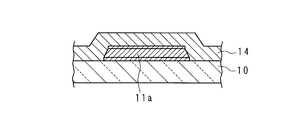
- FIG. 3 is a plan view showing the relationship between the gate wiring 11 of the active matrix substrate 37, the contact hole 14a of the interlayer insulating film 14, and the adjustment hole 14b
- FIG. 4 is a sectional view taken along line IV-IV in FIG. 3
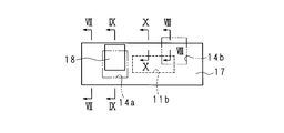
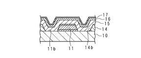
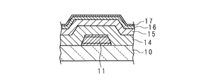
- FIG. FIG. 6 is a plan view showing the relationship between the second semiconductor film 17 when the second semiconductor film 17 is formed, the contact hole 14a of the interlayer insulating film 14, and the adjustment hole 14b.
- 7 is a sectional view taken along line VII-VII in FIG. 6
- FIG. 8 is a sectional view taken along line VIII-VIII in FIG. 6
- FIG. 9 is a sectional view taken along line IX-IX in FIG. It is.
- a gate wiring 11 is formed on the substrate 10 of the active matrix substrate 37 so as to be described later so as to extend in the lateral direction of FIG. 3, and the substrate 10 is formed at a substantially central portion of FIG. A hole 11b extending in the lateral direction in an exposed state is formed. A portion on one end side of the gate wiring 11 becomes a gate electrode 11a.
- An interlayer insulating film 14 is formed so as to cover the substrate 10 as described later.
- the interlayer insulating film 14 is formed so as to extend from the substrate 10 to the periphery of the gate electrode 11a, and a contact hole 14a is provided inside the periphery.
- the interlayer insulating film 14 is provided with an alignment hole (adjustment hole) 14b so that the edge portion at the upper right corner of the hole 11b shown in FIG. 3 is exposed.
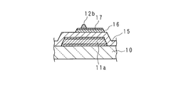
- a gate insulating film 15 is formed on the interlayer insulating film 14 and on the portion of the substrate 10 where the contact hole 14a, the hole 11b, and the adjustment hole 14b are provided.
- the gate insulating film 15 is formed by forming and patterning a film using, for example, silicon oxide or silicon nitride by a CVD (Chemical Vapor Deposition) method.
- the interlayer insulating film 14 has a heat resistance of 350 ° C. or higher, and does not change its physical properties even when it receives a thermal history of the gate insulating film 15 deposition process.
- a first semiconductor film 16 made of, for example, amorphous silicon, for example, a second semiconductor film 17 made of, for example, n + amorphous silicon is sequentially formed by CVD.
- a resist pattern 18 is formed so as to extend from the portion of the second semiconductor film 17 on the contact hole 14a to the edge portion.
- the edge part of the resist pattern 18 is located inside the edge part of the upper surface of the gate electrode 11a.
- the first semiconductor film 16 and the second semiconductor film 17 are patterned using a resist pattern 18.
- a film of Cu or the like is deposited on the patterned second semiconductor film 17 or on the gate insulating film 15 exposed by removing the first semiconductor film 16 and the second semiconductor film 17 by, for example, a sputtering method. Then, patterning is performed to form a source metal including a source electrode and a source wiring (not shown).
- a film of silicon nitride or the like is formed on the source metal by, for example, a CVD method, and a passivation film is formed by patterning (not shown), and a film made of, for example, an acrylic resin is formed on the passivation film, By patterning, a second interlayer insulating film (not shown) is formed.
- the above-described pixel electrode 20 is formed by forming an ITO film on the second interlayer insulating film by sputtering, for example, and patterning.
- FIG. 11 is a schematic cross-sectional view showing a step of forming the interlayer insulating film 14.
- a metal film in which, for example, a titanium film, a Cu film, and a titanium film are sequentially stacked is formed on the entire substrate 10 by sputtering, and then photolithography using a photomask, wet etching of the metal film is performed.
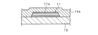
- a patterned gate wiring (a portion to be the gate electrode 11a is also formed) 11 is formed (FIG. 11A).
- a photosensitive SOG material is applied onto the gate wiring 11 by slit coating to form a film 14e (FIG. 11B).
- the SOG material include a composition containing at least two kinds of polysiloxanes, diazonaphthoquinone derivatives, and solvents having different solubility in an aqueous solution of tetramethylammonium hydroxide (TMAH).
- TMAH tetramethylammonium hydroxide
- polysiloxane As the two types of polysiloxane, the following mixtures of polysiloxane (I) and polysiloxane (II) can be mentioned.
- Polysiloxane (I) is a pre-baked film obtained by hydrolysis and condensation of a silane compound represented by the following formula (1) and a silane compound represented by the following formula (2) in the presence of a basic catalyst. Is soluble in a 5% by mass TMAH solution, and its solubility is 1000 kg / sec or less.
- RSi (OR 1 ) 3 (1) Si (OR 1 ) 4 (2) In the formula, R is a linear, branched or cyclic alkyl group having 1 to 20 carbon atoms in which arbitrary methylene may be replaced with oxygen, or an arbitrary hydrogen in which 6 to 20 carbon atoms are replaced with fluorine. R 1 represents an alkyl group having 1 to 5 carbon atoms.
- silane compound represented by the general formula (1) examples include methyltrimethoxysilane, methyltriethoxysilane, phenyltrimethoxysilane, and phenyltriethoxysilane.
- silane compound represented by the general formula (2) examples include tetramethoxysilane and tetraethoxysilane.
- Polysiloxane (II) has a solubility in a 2.38 mass% TMAH aqueous solution of a pre-baked film obtained by hydrolyzing and condensing at least a silane compound of the general formula (1) in the presence of an acidic or basic catalyst. / Second or more.
- the film thickness is adjusted by pre-baking, for example, at 100 ° C. for 90 seconds.
- pre-baking the film 14a is exposed using a photomask, and after exposure, developed with a 2.38% TMAH aqueous solution. As a result, a pattern is formed in which the contact holes 14a are left without any residue.
- post-baking is performed at 250 ° C., and the film 14e is cured to obtain the interlayer insulating film 14 (FIG. 11C).
- the interlayer insulating film 14 is formed using a photosensitive SOG material, dry etching is not required for the film formation, and the surface of the substrate 10 is manufactured as in the case of manufacturing a conventional active matrix substrate. There will be no problem of scraping or abnormal discharge. Therefore, the adjustment hole 14 b described above can be provided in a portion of the interlayer insulating film 14 other than on the gate wiring 11.
- the edge of the gate electrode 11a can be visually recognized from the adjustment hole 14b.
- the deviation of the position of the resist pattern 18 from the edge is measured, the photoresist is re-formed based on the measured deviation, exposed using a photo mask, developed, and the resist pattern 18 is re-formed.
- the portions of the first semiconductor film 16 and the second semiconductor film 17 where the pattern 18 is not formed can be etched to pattern the first semiconductor film 16 and the second semiconductor film 17.
- the position of the resist pattern formed on the source metal with respect to the gate wiring 11 is confirmed from the adjustment hole 14b, and the position of the resist pattern is determined.
- the source metal can be patterned by adjusting.
- the gate insulating film 15 can be formed by confirming the position of the edge of the gate wiring 11 by the adjustment hole 14b, and the first semiconductor film 16, the second semiconductor film 17, and the source metal are also formed as described above. The position of the edge of 11 can be confirmed and formed. That is, since the overlay can be adjusted with reference to the film pattern of the gate wiring 11, the overlay accuracy is good. Position adjustment can be easily performed, the number of condition settings can be reduced, the occurrence of defects can be suppressed, and the active matrix substrate 37 can be manufactured with a good yield. Since the position accuracy of film formation of the active matrix substrate 37 is good, the display module 91 including the active matrix substrate 37 according to the present embodiment can be realized with high definition and large size.
- FIG. 12 is a plan view showing the relationship between the gate wiring 11 and the contact hole 14a and the adjustment holes 14b and 14c of the interlayer insulating film 14, and FIG. 14a is a plan view showing a relationship with the adjustment holes 14b and 14c.
- the interlayer insulating film 14 is provided with an adjustment hole 14c so that the lower right corner of the hole 11b of the gate wiring 11 shown in FIG. 12 is exposed.
- the interlayer insulating film 14 has the two adjustment holes 14b and 14c, for example, in the lateral direction with reference to two edges of the lowermost gate wiring 11 provided immediately above the substrate 10 And the vertical alignment can be adjusted by the respective adjustment holes, and the overlay adjustment of all the films formed on the gate wiring 11 can be adjusted more reliably. Therefore, the overlay accuracy is better.
- Embodiment 3 FIG.
- the active matrix substrate according to the second embodiment of the present invention has the same configuration as the active matrix substrate 37 according to the first embodiment except that the shape and size of the contact holes 14d provided in the interlayer insulating film 14 are different.
- FIG. 14 is a plan view showing the relationship between the gate wiring 11 and the contact hole 14d of the interlayer insulating film 14, and FIG. 15 shows the relationship between the second semiconductor film 17 and the contact hole 14d when the second semiconductor film 17 is formed.
- FIG. 16 is a plan view taken along the line XVI--XVI in FIG.
- the contact hole 14 d of the interlayer insulating film 14 is provided to be wider than the width of the gate wiring 11.
- the gate insulating film 15 is formed on the interlayer insulating film 14, the bottom surface of the contact hole 14 d, and the gate wiring 11, and the first semiconductor film 16 and the second semiconductor film 16 are formed on the gate insulating film 15.
- the semiconductor film 17 is formed sequentially.
- a resist pattern 18 is provided on the contact hole 14 d of the second semiconductor film 17.
- the edge of the gate wiring 11 on the contact hole 14d is visually recognized, the deviation of the position of the resist pattern 18 from the edge is measured, the resist pattern 18 is re-formed, and the first The semiconductor film 16 and the second semiconductor film 17 can be patterned. Even when a source metal film is formed on the patterned second semiconductor film 17 and patterned, the edge of the gate wiring 11 on the contact hole 14d can be visually recognized and the pattern can be adjusted.
- Embodiment 4 FIG.
- the interlayer insulating film 14 is formed only in the portion where the gate wiring 11 and the source metal 12 intersect.
- 17 is a plan view showing the formation positions of the gate wiring 11, the interlayer insulating film 14 and the source wiring 12a
- FIG. 18 is a cross-sectional view taken along the line XVIII-XVIII in FIG. 17
- FIG. 19 is a cross-sectional view taken along the line XIX-XIX in FIG. is there.
- the interlayer insulating film 14 is formed only in a portion where the gate wiring 11 and the source wiring 12a intersect.
- a gate insulating film 15 is formed on the interlayer insulating film 14 and above the portions of the substrate 10 and the gate wiring 11 where the interlayer insulating film 14 is not formed.
- a first semiconductor film 16 and a second semiconductor film 17 are formed on the gate insulating film 15 formed on the gate electrode 11 a, and a source electrode 12 b is formed on the second semiconductor film 17.
- the interlayer insulating film 14 is formed only at a portion where the gate wiring 11 and the source wiring 12 intersect, the first semiconductor film 16 and the second semiconductor film 17 are formed, and the source When the wiring 12a and the source electrode 12b are formed, the edge of the gate wiring 11 can be confirmed and patterning can be adjusted.
- the laminated structure of the active matrix substrate is not limited to the above-described case, and any appropriate film material can be used except that the interlayer insulating film 14 is formed of a photosensitive SOG material. .
Landscapes
- Physics & Mathematics (AREA)
- Nonlinear Science (AREA)
- General Physics & Mathematics (AREA)
- Chemical & Material Sciences (AREA)
- Crystallography & Structural Chemistry (AREA)
- Mathematical Physics (AREA)
- Optics & Photonics (AREA)
- Engineering & Computer Science (AREA)
- Microelectronics & Electronic Packaging (AREA)
- Spectroscopy & Molecular Physics (AREA)
- Liquid Crystal (AREA)
- Thin Film Transistor (AREA)
- Devices For Indicating Variable Information By Combining Individual Elements (AREA)
Abstract
Description
ゲート配線とソース配線との交叉部分に形成される容量(寄生容量)は、表示品位の低下の原因となるため、小さくすることが好ましい。
特許文献1には、ゲート配線を覆う絶縁膜を、第1絶縁層と第2絶縁層とを有する多層絶縁膜にし、第1絶縁層を有機成分を含む絶縁材料から構成することにより、前記寄生容量の低減を図ったアクティブマトリクス基板の発明が開始されている。
図20に示すように、アクティブマトリクス基板のガラス製の基板10上に、ゲート電極11a(ゲート配線11の一部をなす)が形成されている。
SOGからなる層間絶縁膜14は基板10、及びゲート電極11aの周縁部を覆うように形成されている。層間絶縁膜14の、ゲート電極11aの周縁部の内側には、層間絶縁膜14に覆われていないコンタクトホール14aが設けられている。
この第1半導体膜16及び第2半導体膜17をパターニングするために、レジストパターン18が形成されている。
以上のTFT構造において、ゲート配線11とソース配線との間に層間絶縁層14を設けることで、配線抵抗の増加及びTFT駆動の低下を伴わずに高精細な表示パネルを製造することが可能となる。
これから形成する第1半導体膜16及び第2半導体膜17のパターンの位置の補正をするためにレジストパターン18を補正する。このとき、顕微鏡により、レジストパターン18のゲート配線11の縁部からの距離を計測する。この結果に基づいてフォトレジストを再度形成し、フォトマスクを用いてレジストパターン18を形成し直した後、レジストパターン18で覆われていない部分をエッチングして、パターン化された第1半導体膜16及び第2半導体膜17を得る。
図21Aに示すように、SOGからなる層間絶縁膜14が存在しない場合、ゲート配線11の縁部が視認されるので、レジストパターン18の位置調整を容易に行うことができる。
従って、ゲート配線11上以外に、層間絶縁膜14にアライメント用の孔を形成することはできないという問題があった。
そして、本発明によれば、位置調整が容易になり、不良の発生が抑制され、歩留りが良好な状態でアクティブマトリクス基板を製造することができる。
そして、本発明によれば、位置調整が容易になり、不良の発生が抑制され、歩留りが良好な状態でアクティブマトリクス基板を製造することができ、高精細な表示装置を得ることができ、表示装置の大型化にも対応することができる。
実施の形態1.
図1は、本発明に係る液晶表示装置(表示モジュール91)を備えるTV受信機90を示す概略斜視図、図2は表示モジュール91が有する表示パネル30を示す概略断面図である。
表示モジュール91は、前後に縦姿勢で配置された前キャビネット92及び後キャビネット93に縦姿勢で収容されている。前キャビネット92は表示モジュール91の周縁部を覆う矩形状の枠体であり、後キャビネット93は、前側が開放された矩形のトレイ状をなす。
基板10上にゲート配線11が形成され、基板10及びゲート配線11を覆うように層間絶縁膜14が形成されている。層間絶縁膜14上に複数の画素電極20が形成され、該画素電極20を覆うように透明の配向膜31が形成されている。画素電極20はアクティブマトリクスとともに形成され、図2においてはアクティブマトリクスのゲート配線11を示している。基板10、ゲート配線11、層間絶縁膜14、及び画素電極20を含んでアクティブマトリクス基板(TFT基板)37が構成される。ここで、層間絶縁膜14と画素電極20との間の膜は省略している。
そして、液晶層36を狭持するように配向膜31,35が貼り合わせられて基板10,32が固定され、基板10,32の外側に偏光板39,40が設けられている。
そして、層間絶縁膜14には、図3に示す孔11bの右上角の縁部分が露出するように、アライメント用の孔(調整孔)14bが設けられている。
第2の層間絶縁膜上に、例えばスパッタリング法によりITO膜を形成し、パターニングすることにより上述の画素電極20が形成される。
まず、基板10の全体に、スパッタリング法により、例えば、チタン膜、Cu膜、及びチタン膜等を順に積層した金属膜を成膜し、その後、フォトマスクを用いたフォトリソグラフィ、金属膜のウエットエッチング等を行うことにより、パターン化されたゲート配線(ゲート電極11aとなる部分も形成される)11を形成する(図11A)。
ここで、SOG材料としては、テトラメチルアンモニウムヒドロキシド(TMAH)水溶液に対する溶解度が異なる少なくとも2種類以上のポリシロキサン、ジアゾナフトキノン誘導体、及び溶剤を含有する組成物が挙げられる。
RSi(OR1 )3 ・・・(1)
Si(OR1 )4 ・・・(2)
(式中、Rは任意のメチレンが酸素で置き換えられてもよい炭素数1~20の直鎖状、分岐状若しくは環状アルキル基、又は炭素数6~20で任意の水素がフッ素で置き換えられてもよいアリール基を表し、R1 は炭素数1~5のアルキル基を表す。)
一般式(1)で表わされるシラン化合物の具体例としては、例えばメチルトリメトキシシラン、メチルトリエトキシシラン、フェニルトリメトキシシラン、フェニルトリエトキシシラン等が挙げられる。
一般式(2)で表わされるシラン化合物の具体例としては、例えばテトラメトキシシラン、テトラエトキシシラン等が挙げられる。
プリベーク後、フォトマスクを用いて膜14aに露光し、露光後、2.38%TMAH水溶液により現像する。これにより、コンタクトホール14aが、残渣等なく抜けたパターンが形成される。
そして、例えば250℃でポストベークし、膜14eを硬化させて層間絶縁膜14を得る(図11C)。
すなわち、ゲート配線11の膜のパターンを基準にして、重ね合わせの調整を行うことができるので、重ね合わせの精度が良好である。
位置調整は容易に行うことができ、条件設定の回数も減じることができ、不良の発生が抑制され、歩留りが良好な状態でアクティブマトリクス基板37を製造することができる。
アクティブマトリクス基板37の成膜の位置精度が良好であるので、本実施の形態に係るアクティブマトリクス基板37を備える表示モジュール91は高精細化、及び大型化が実現され得る。
本発明の実施の形態2に係るアクティブマトリクス基板においては、層間絶縁膜14が調整孔を2つ有すること以外は、実施の形態1に係るアクティブマトリクス基板37と同様の構成を有する。
図12はゲート配線11と層間絶縁膜14のコンタクトホール14a、調整孔14b,14cとの関係を示す平面図、図13は第2半導体膜17を形成した場合の第2半導体膜17とコンタクトホール14a、調整孔14b,14cとの関係を示す平面図である。
層間絶縁膜14には、調整孔14bに加えて、図12に示すゲート配線11の孔11bの右下角の縁部分が露出するように、調整孔14cが設けられている。
本発明の実施の形態2に係るアクティブマトリクス基板は、層間絶縁膜14に設けられたコンタクトホール14dの形状及び大きさが異なること以外は、実施の形態1に係るアクティブマトリクス基板37と同様の構成を有する。
そして、パターニングされた第2半導体膜17上にソースメタル用の膜を形成し、パターニングする場合においても、コンタクトホール14d上のゲート配線11の縁部を視認しパターンの調整を行うことができる。
本実施の形態においては、ゲート配線11とソースメタル12とが交叉する部分のみに層間絶縁膜14が形成されている。
図17はゲート配線11、層間絶縁膜14、及びソース配線12aの形成位置を示す平面図、図18は図17のXVIII -XVIII線断面図、図19は図17のXIX -XIX 線断面図である。
層間絶縁膜14上、並びに層間絶縁膜14が形成されていない基板10及びゲート配線11の部分の上側には、ゲート絶縁膜15が形成されている。
ゲート電極11a上に形成されたゲート絶縁膜15上には、第1半導体膜16及び第2半導体膜17が形成され、第2半導体膜17上にはソース電極12bが形成されている。
例えばアクティブマトリクス基板の積層構造は上述した場合に限定されるものではなく、また、層間絶縁膜14が感光性を有するSOG材料から形成されること以外は、適宜の膜材料を使用することができる。
11 ゲート配線
11a ゲート電極
11b 孔
12 ソースメタル
12a ソース配線
12b ソース電極
14 層間絶縁膜
14a、14d コンタクトホール
14b、14c 調整孔
20 画素電極
30 表示パネル
31、35 配向膜
32 基板
33 カラーフィルタ
34 共通電極
36 液晶層
37 アクティブマトリクス基板
38 カラーフィルタ基板
39、40 偏光板
90 TV受信機
91 表示モジュール
92 前キャビネット
93 後キャビネット
94 チューナ
95 デコーダ
96 スタンド
Claims (9)
- 基板上に、複数のゲート配線と複数のソース配線とを立体的に交叉するように形成し、前記ゲート配線と前記ソース配線とが交叉する部分の近傍に薄膜トランジスタを形成し、少なくとも前記ゲート配線と前記ソース配線との間に、スピンオンガラス(SOG)材料を含んでなる層間絶縁膜を形成するアクティブマトリクス基板の製造方法において、
前記層間絶縁膜は、感光性を有するSOG材料を用い、前記基板及び前記層間絶縁膜の上側に形成する膜のパターンを調整するための孔を有するように形成することを特徴とするアクティブマトリクス基板の製造方法。 - 前記層間絶縁膜を形成するに先立ち、前記基板上に前記ゲート配線を形成する工程を有し、
前記孔は、前記ゲート配線の縁部を視認可能に形成することを特徴とする請求項1に記載のアクティブマトリクス基板の製造方法。 - 前記孔は、前記ゲート配線の縁部を跨ぐように形成することを特徴とする請求項2に記載のアクティブマトリクス基板の製造方法。
- 前記孔により、前記ゲート配線の縁部を視認して、前記ゲート配線の上側に半導体膜を形成する工程を有することを特徴とする請求項2又は3に記載のアクティブマトリクス基板の製造方法。
- 前記孔により、前記ゲート配線の縁部を視認して、前記半導体膜の上側に前記ソース配線又はソース電極を含むソースメタルを形成する工程を有することを特徴とする請求項4に記載のアクティブマトリクス基板の製造方法。
- 基板上に、複数のゲート配線と複数のソース配線とを立体的に交叉するように形成し、前記ゲート配線と前記ソース配線とが交叉する部分の近傍に薄膜トランジスタを形成するアクティブマトリクス基板の製造方法において、
前記基板上に前記ゲート配線を形成し、
前記ソース配線と交叉する前記ゲート配線の部分の表面に、感光性を有するSOG材料を用いて層間絶縁膜を形成し、
前記ゲート配線の縁部を視認して、前記層間絶縁膜上、前記基板上、及び前記ゲート配線上に成膜することを特徴とするアクティブマトリクス基板の製造方法。 - 前記SOG材料は、
テトラメチルアンモニウムヒドロキシド水溶液に対する溶解速度が異なる少なくとも2種類以上のポリシロキサン、ジアゾナフトキノン誘導体、及び溶剤を含有することを特徴とする請求項1から6までのいずれか1項に記載のアクティブマトリクス基板の製造方法。 - 基板上に、複数のゲート配線と複数のソース配線とを立体的に交叉するように形成し、前記ゲート配線と前記ソース配線とが交叉する部分の近傍に薄膜トランジスタを形成し、少なくとも前記ゲート配線と前記ソース配線との間に、スピンオンガラス(SOG)材料を含んでなる層間絶縁膜が介在するアクティブマトリクス基板において、
前記層間絶縁膜は、感光性を有するSOG材料を用いてなり、前記基板及び前記層間絶縁膜の上側に形成する膜のパターン調整孔を有することを特徴とするアクティブマトリクス基板。 - 請求項8に記載のアクティブマトリクス基板と、
該アクティブマトリクス基板上に配置された表示媒体層と、
前記アクティブマトリクス基板に前記表示媒体層を介して対向する対向基板と
を備えることを特徴とする表示装置。
Priority Applications (4)
| Application Number | Priority Date | Filing Date | Title |
|---|---|---|---|
| JP2015556666A JP6006889B2 (ja) | 2014-01-08 | 2014-01-08 | アクティブマトリクス基板の製造方法、アクティブマトリクス基板、及び表示装置 |
| US15/110,081 US10115746B2 (en) | 2014-01-08 | 2014-01-08 | Manufacturing method for active matrix substrate, active matrix substrate and display apparatus |
| CN201480072505.7A CN105900001B (zh) | 2014-01-08 | 2014-01-08 | 有源矩阵基板、有源矩阵基板的制造方法和显示装置 |
| PCT/JP2014/050166 WO2015104806A1 (ja) | 2014-01-08 | 2014-01-08 | アクティブマトリクス基板の製造方法、アクティブマトリクス基板、及び表示装置 |
Applications Claiming Priority (1)
| Application Number | Priority Date | Filing Date | Title |
|---|---|---|---|
| PCT/JP2014/050166 WO2015104806A1 (ja) | 2014-01-08 | 2014-01-08 | アクティブマトリクス基板の製造方法、アクティブマトリクス基板、及び表示装置 |
Publications (1)
| Publication Number | Publication Date |
|---|---|
| WO2015104806A1 true WO2015104806A1 (ja) | 2015-07-16 |
Family
ID=53523658
Family Applications (1)
| Application Number | Title | Priority Date | Filing Date |
|---|---|---|---|
| PCT/JP2014/050166 Ceased WO2015104806A1 (ja) | 2014-01-08 | 2014-01-08 | アクティブマトリクス基板の製造方法、アクティブマトリクス基板、及び表示装置 |
Country Status (4)
| Country | Link |
|---|---|
| US (1) | US10115746B2 (ja) |
| JP (1) | JP6006889B2 (ja) |
| CN (1) | CN105900001B (ja) |
| WO (1) | WO2015104806A1 (ja) |
Cited By (2)
| Publication number | Priority date | Publication date | Assignee | Title |
|---|---|---|---|---|
| CN105319792A (zh) * | 2015-11-16 | 2016-02-10 | 深圳市华星光电技术有限公司 | 阵列基板及液晶显示面板 |
| JP2019070768A (ja) * | 2017-10-11 | 2019-05-09 | シャープ株式会社 | アレイ基板およびその製造方法、並びに表示パネル |
Families Citing this family (1)
| Publication number | Priority date | Publication date | Assignee | Title |
|---|---|---|---|---|
| US10983398B2 (en) * | 2018-01-19 | 2021-04-20 | Sakai Display Products Corporation | Method for manufacturing liquid crystal display device and photomask |
Citations (3)
| Publication number | Priority date | Publication date | Assignee | Title |
|---|---|---|---|---|
| JPH08146400A (ja) * | 1994-11-16 | 1996-06-07 | Seiko Epson Corp | 液晶表示装置及び液晶表示装置の製造方法 |
| JPH11352514A (ja) * | 1998-06-09 | 1999-12-24 | Hitachi Ltd | 液晶表示装置 |
| JP2009086086A (ja) * | 2007-09-28 | 2009-04-23 | Sharp Corp | 表示パネル用の基板、表示パネル、表示パネル用基板の製造方法および表示パネルの製造方法 |
Family Cites Families (5)
| Publication number | Priority date | Publication date | Assignee | Title |
|---|---|---|---|---|
| WO2006022259A1 (ja) | 2004-08-24 | 2006-03-02 | Sharp Kabushiki Kaisha | アクティブマトリクス基板およびそれを備えた表示装置 |
| WO2011132376A1 (ja) * | 2010-04-21 | 2011-10-27 | シャープ株式会社 | 薄膜トランジスタ基板 |
| DE112011102793B4 (de) * | 2010-08-24 | 2023-01-12 | Merck Patent Gmbh | Positiv arbeitende lichtempfindliche Siloxanzusammensetzung, daraus gebildeter gehärteter Film und Element mit diesem |
| US20130021695A1 (en) * | 2011-07-20 | 2013-01-24 | Taisuke Sugii | Base design of magnetic disk drive |
| JP6308757B2 (ja) * | 2013-11-20 | 2018-04-11 | 三菱電機株式会社 | 液晶表示パネルおよび液晶表示パネルの製造方法 |
-
2014
- 2014-01-08 US US15/110,081 patent/US10115746B2/en not_active Expired - Fee Related
- 2014-01-08 CN CN201480072505.7A patent/CN105900001B/zh not_active Expired - Fee Related
- 2014-01-08 WO PCT/JP2014/050166 patent/WO2015104806A1/ja not_active Ceased
- 2014-01-08 JP JP2015556666A patent/JP6006889B2/ja not_active Expired - Fee Related
Patent Citations (3)
| Publication number | Priority date | Publication date | Assignee | Title |
|---|---|---|---|---|
| JPH08146400A (ja) * | 1994-11-16 | 1996-06-07 | Seiko Epson Corp | 液晶表示装置及び液晶表示装置の製造方法 |
| JPH11352514A (ja) * | 1998-06-09 | 1999-12-24 | Hitachi Ltd | 液晶表示装置 |
| JP2009086086A (ja) * | 2007-09-28 | 2009-04-23 | Sharp Corp | 表示パネル用の基板、表示パネル、表示パネル用基板の製造方法および表示パネルの製造方法 |
Cited By (3)
| Publication number | Priority date | Publication date | Assignee | Title |
|---|---|---|---|---|
| CN105319792A (zh) * | 2015-11-16 | 2016-02-10 | 深圳市华星光电技术有限公司 | 阵列基板及液晶显示面板 |
| CN105319792B (zh) * | 2015-11-16 | 2019-01-04 | 深圳市华星光电技术有限公司 | 阵列基板及液晶显示面板 |
| JP2019070768A (ja) * | 2017-10-11 | 2019-05-09 | シャープ株式会社 | アレイ基板およびその製造方法、並びに表示パネル |
Also Published As
| Publication number | Publication date |
|---|---|
| US10115746B2 (en) | 2018-10-30 |
| JP6006889B2 (ja) | 2016-10-12 |
| US20160336357A1 (en) | 2016-11-17 |
| JPWO2015104806A1 (ja) | 2017-03-23 |
| CN105900001A (zh) | 2016-08-24 |
| CN105900001B (zh) | 2017-12-29 |
Similar Documents
| Publication | Publication Date | Title |
|---|---|---|
| KR101905757B1 (ko) | 에프에프에스 방식 액정표시장치용 어레이기판 및 그 제조방법 | |
| KR101446249B1 (ko) | 반도체장치 제조방법 | |
| US20120086881A1 (en) | Array substrate for liquid crystal display device and fabrication method thereof | |
| JP6238712B2 (ja) | 薄膜トランジスタ基板およびその製造方法 | |
| CN105137665A (zh) | 显示基板及其制备方法、显示装置 | |
| WO2017166341A1 (zh) | Tft基板的制作方法及制得的tft基板 | |
| WO2015081652A1 (zh) | 阵列基板及其制作方法、显示装置 | |
| US20120280239A1 (en) | Thin film transistor array substrate and method for fabricating the thin film transistor array substrate | |
| JP2004318063A (ja) | 液晶表示装置用基板及びそれを用いた液晶表示装置 | |
| US7876390B2 (en) | Liquid crystal display fabrication method | |
| US20110128459A1 (en) | Thin film transistor array substrate, fabrication method thereof, and liquid crystal display using the tft array substrate | |
| WO2020133651A1 (zh) | 像素电极结构及其制作方法 | |
| CN105655290A (zh) | 液晶显示面板、阵列基板及其制造方法 | |
| US20080206911A1 (en) | Method of manufacturing liquid crystal display | |
| CN107209456A (zh) | 正型感光性硅氧烷组合物、有源矩阵基板、显示装置以及有源矩阵基板的制造方法 | |
| JP6006889B2 (ja) | アクティブマトリクス基板の製造方法、アクティブマトリクス基板、及び表示装置 | |
| CN101676781A (zh) | 影像显示系统及其制造方法 | |
| JP2015099287A (ja) | 液晶表示パネルおよび液晶表示パネルの製造方法 | |
| JP5048914B2 (ja) | 薄膜トランジスタ表示板の製造方法 | |
| WO2015064426A1 (ja) | アクティブマトリクス基板、表示装置、及びアクティブマトリクス基板の製造方法 | |
| JP2001264798A (ja) | アクティブマトリックス基板及びそれを用いた光学変調素子 | |
| CN1794066A (zh) | 薄膜晶体管阵列面板及其制造方法 | |
| KR101369571B1 (ko) | 어레이 기판, 그 제조 방법 및 액정 디스플레이 | |
| CN109491157B (zh) | 显示面板用基板的制造方法 | |
| WO2006109585A1 (ja) | 導電層を備えた基板、表示装置および導電層を備えた基板の製造方法 |
Legal Events
| Date | Code | Title | Description |
|---|---|---|---|
| 121 | Ep: the epo has been informed by wipo that ep was designated in this application |
Ref document number: 14877912 Country of ref document: EP Kind code of ref document: A1 |
|
| ENP | Entry into the national phase |
Ref document number: 2015556666 Country of ref document: JP Kind code of ref document: A |
|
| WWE | Wipo information: entry into national phase |
Ref document number: 15110081 Country of ref document: US |
|
| NENP | Non-entry into the national phase |
Ref country code: DE |
|
| 122 | Ep: pct application non-entry in european phase |
Ref document number: 14877912 Country of ref document: EP Kind code of ref document: A1 |