WO2015097973A1 - 有機elパネルユニットおよび有機el表示装置 - Google Patents
有機elパネルユニットおよび有機el表示装置 Download PDFInfo
- Publication number
- WO2015097973A1 WO2015097973A1 PCT/JP2014/005731 JP2014005731W WO2015097973A1 WO 2015097973 A1 WO2015097973 A1 WO 2015097973A1 JP 2014005731 W JP2014005731 W JP 2014005731W WO 2015097973 A1 WO2015097973 A1 WO 2015097973A1
- Authority
- WO
- WIPO (PCT)
- Prior art keywords
- organic
- panel
- sheet member
- sheet
- back surface
- Prior art date
- Legal status (The legal status is an assumption and is not a legal conclusion. Google has not performed a legal analysis and makes no representation as to the accuracy of the status listed.)
- Ceased
Links
Images









Classifications
-
- H—ELECTRICITY
- H10—SEMICONDUCTOR DEVICES; ELECTRIC SOLID-STATE DEVICES NOT OTHERWISE PROVIDED FOR
- H10K—ORGANIC ELECTRIC SOLID-STATE DEVICES
- H10K77/00—Constructional details of devices covered by this subclass and not covered by groups H10K10/80, H10K30/80, H10K50/80 or H10K59/80
- H10K77/10—Substrates, e.g. flexible substrates
-
- H—ELECTRICITY
- H10—SEMICONDUCTOR DEVICES; ELECTRIC SOLID-STATE DEVICES NOT OTHERWISE PROVIDED FOR
- H10K—ORGANIC ELECTRIC SOLID-STATE DEVICES
- H10K50/00—Organic light-emitting devices
- H10K50/80—Constructional details
- H10K50/84—Passivation; Containers; Encapsulations
-
- H—ELECTRICITY
- H10—SEMICONDUCTOR DEVICES; ELECTRIC SOLID-STATE DEVICES NOT OTHERWISE PROVIDED FOR
- H10K—ORGANIC ELECTRIC SOLID-STATE DEVICES
- H10K50/00—Organic light-emitting devices
- H10K50/80—Constructional details
- H10K50/87—Arrangements for heating or cooling
-
- H—ELECTRICITY
- H10—SEMICONDUCTOR DEVICES; ELECTRIC SOLID-STATE DEVICES NOT OTHERWISE PROVIDED FOR
- H10K—ORGANIC ELECTRIC SOLID-STATE DEVICES
- H10K59/00—Integrated devices, or assemblies of multiple devices, comprising at least one organic light-emitting element covered by group H10K50/00
- H10K59/80—Constructional details
- H10K59/87—Passivation; Containers; Encapsulations
-
- H—ELECTRICITY
- H10—SEMICONDUCTOR DEVICES; ELECTRIC SOLID-STATE DEVICES NOT OTHERWISE PROVIDED FOR
- H10K—ORGANIC ELECTRIC SOLID-STATE DEVICES
- H10K59/00—Integrated devices, or assemblies of multiple devices, comprising at least one organic light-emitting element covered by group H10K50/00
- H10K59/80—Constructional details
- H10K59/8794—Arrangements for heating and cooling
-
- G—PHYSICS
- G09—EDUCATION; CRYPTOGRAPHY; DISPLAY; ADVERTISING; SEALS
- G09G—ARRANGEMENTS OR CIRCUITS FOR CONTROL OF INDICATING DEVICES USING STATIC MEANS TO PRESENT VARIABLE INFORMATION
- G09G2300/00—Aspects of the constitution of display devices
- G09G2300/08—Active matrix structure, i.e. with use of active elements, inclusive of non-linear two terminal elements, in the pixels together with light emitting or modulating elements
- G09G2300/0809—Several active elements per pixel in active matrix panels
- G09G2300/0842—Several active elements per pixel in active matrix panels forming a memory circuit, e.g. a dynamic memory with one capacitor
-
- G—PHYSICS
- G09—EDUCATION; CRYPTOGRAPHY; DISPLAY; ADVERTISING; SEALS
- G09G—ARRANGEMENTS OR CIRCUITS FOR CONTROL OF INDICATING DEVICES USING STATIC MEANS TO PRESENT VARIABLE INFORMATION
- G09G2330/00—Aspects of power supply; Aspects of display protection and defect management
- G09G2330/04—Display protection
- G09G2330/045—Protection against panel overheating
-
- G—PHYSICS
- G09—EDUCATION; CRYPTOGRAPHY; DISPLAY; ADVERTISING; SEALS
- G09G—ARRANGEMENTS OR CIRCUITS FOR CONTROL OF INDICATING DEVICES USING STATIC MEANS TO PRESENT VARIABLE INFORMATION
- G09G2380/00—Specific applications
- G09G2380/02—Flexible displays
-
- G—PHYSICS
- G09—EDUCATION; CRYPTOGRAPHY; DISPLAY; ADVERTISING; SEALS
- G09G—ARRANGEMENTS OR CIRCUITS FOR CONTROL OF INDICATING DEVICES USING STATIC MEANS TO PRESENT VARIABLE INFORMATION
- G09G3/00—Control arrangements or circuits, of interest only in connection with visual indicators other than cathode-ray tubes
- G09G3/20—Control arrangements or circuits, of interest only in connection with visual indicators other than cathode-ray tubes for presentation of an assembly of a number of characters, e.g. a page, by composing the assembly by combination of individual elements arranged in a matrix no fixed position being assigned to or needed to be assigned to the individual characters or partial characters
- G09G3/22—Control arrangements or circuits, of interest only in connection with visual indicators other than cathode-ray tubes for presentation of an assembly of a number of characters, e.g. a page, by composing the assembly by combination of individual elements arranged in a matrix no fixed position being assigned to or needed to be assigned to the individual characters or partial characters using controlled light sources
- G09G3/30—Control arrangements or circuits, of interest only in connection with visual indicators other than cathode-ray tubes for presentation of an assembly of a number of characters, e.g. a page, by composing the assembly by combination of individual elements arranged in a matrix no fixed position being assigned to or needed to be assigned to the individual characters or partial characters using controlled light sources using electroluminescent panels
- G09G3/32—Control arrangements or circuits, of interest only in connection with visual indicators other than cathode-ray tubes for presentation of an assembly of a number of characters, e.g. a page, by composing the assembly by combination of individual elements arranged in a matrix no fixed position being assigned to or needed to be assigned to the individual characters or partial characters using controlled light sources using electroluminescent panels semiconductive, e.g. using light-emitting diodes [LED]
- G09G3/3208—Control arrangements or circuits, of interest only in connection with visual indicators other than cathode-ray tubes for presentation of an assembly of a number of characters, e.g. a page, by composing the assembly by combination of individual elements arranged in a matrix no fixed position being assigned to or needed to be assigned to the individual characters or partial characters using controlled light sources using electroluminescent panels semiconductive, e.g. using light-emitting diodes [LED] organic, e.g. using organic light-emitting diodes [OLED]
- G09G3/3225—Control arrangements or circuits, of interest only in connection with visual indicators other than cathode-ray tubes for presentation of an assembly of a number of characters, e.g. a page, by composing the assembly by combination of individual elements arranged in a matrix no fixed position being assigned to or needed to be assigned to the individual characters or partial characters using controlled light sources using electroluminescent panels semiconductive, e.g. using light-emitting diodes [LED] organic, e.g. using organic light-emitting diodes [OLED] using an active matrix
-
- Y—GENERAL TAGGING OF NEW TECHNOLOGICAL DEVELOPMENTS; GENERAL TAGGING OF CROSS-SECTIONAL TECHNOLOGIES SPANNING OVER SEVERAL SECTIONS OF THE IPC; TECHNICAL SUBJECTS COVERED BY FORMER USPC CROSS-REFERENCE ART COLLECTIONS [XRACs] AND DIGESTS
- Y02—TECHNOLOGIES OR APPLICATIONS FOR MITIGATION OR ADAPTATION AGAINST CLIMATE CHANGE
- Y02E—REDUCTION OF GREENHOUSE GAS [GHG] EMISSIONS, RELATED TO ENERGY GENERATION, TRANSMISSION OR DISTRIBUTION
- Y02E10/00—Energy generation through renewable energy sources
- Y02E10/50—Photovoltaic [PV] energy
- Y02E10/549—Organic PV cells
Definitions
- This disclosure relates to an organic EL panel unit including an organic EL (Electro Luminescence) panel.
- Patent Document 1 discloses a display device including a heat conductive layer that conducts heat generated in a display panel. The density of the heat conductive layer in this display device is higher in the second region separated from the center point than in the first region including or near the center point of the display region.
- Patent Document 1 discloses that the above configuration suppresses a local temperature increase in the central region of the display panel.
- the present disclosure provides an organic EL panel unit and an organic EL display device that can efficiently dissipate heat from the organic EL panel and can suppress deformation of the organic EL panel due to temperature change.
- the organic EL panel unit includes an organic EL panel that displays an image on the front surface, and a plurality of sheet members that are attached to the back surface of the organic EL panel, and are formed by rolling a metal plate.
- a plurality of sheet members, wherein the plurality of sheet members include a first sheet member and a second sheet member, wherein the first sheet member and the second sheet member are part of one and the other part of the other Are attached to the back surface of the panel so that the rolling directions are different from each other.
- the organic EL panel unit in the present disclosure it is possible to efficiently dissipate heat about the organic EL panel and to suppress deformation of the organic EL panel due to temperature change. Thereby, a high-quality organic EL panel unit, a thin television equipped with the organic EL panel unit, and the like can be provided.
- FIG. 1 is a schematic diagram showing the relationship between the rolling direction of the heat dissipation sheet and the warp direction of the organic EL panel unit.
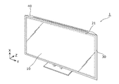
- FIG. 2 is an external perspective view of the organic EL display device according to the embodiment.
- FIG. 3 is an exploded perspective view of the organic EL display device according to the embodiment.
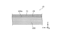
- FIG. 4 is a partial cross-sectional view of the organic EL panel unit in the embodiment.
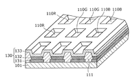
- FIG. 5 is a partially cutaway perspective view of the organic EL panel according to the embodiment.
- FIG. 6 is a perspective view showing an example of a pixel bank of the organic EL panel in the embodiment.
- FIG. 7 is an electric circuit diagram showing a configuration of a pixel circuit of the organic EL panel in the embodiment.
- FIG. 1 is a schematic diagram showing the relationship between the rolling direction of the heat dissipation sheet and the warp direction of the organic EL panel unit.
- FIG. 2 is an external perspective view of the organic EL display device according to the embodiment.
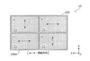
- FIG. 8A is a diagram illustrating an example of a layout of a plurality of sheet members in the embodiment.
- FIG. 8B is a diagram illustrating a bending direction of each of the plurality of sheet members illustrated in FIG. 8A.
- FIG. 9A is a diagram showing a layout of a plurality of sheet members in Modification 1 of the embodiment.
- FIG. 9B is a diagram illustrating a layout of a plurality of sheet members according to the second modification of the embodiment.
- FIG. 9C is a diagram illustrating a layout of a plurality of sheet members according to the third modification of the embodiment.
- FIG. 9D is a diagram showing a layout of a plurality of sheet members in Modification 4 of the embodiment.
- FIG. 9A is a diagram illustrating an example of a layout of a plurality of sheet members in the embodiment.
- FIG. 8B is a diagram illustrating a bending direction of each of the plurality of sheet members illustrated in FIG. 8A.
- FIG. 9A
- FIG. 10A is a diagram illustrating a layout of a plurality of sheet members in Modification 5 of the embodiment.
- FIG. 10B is a diagram illustrating a layout of a plurality of sheet members in Modification 6 of the embodiment.
- FIG. 10C is a diagram showing a layout of a plurality of sheet members in Modification 7 of the embodiment.
- FIG. 11 is a diagram illustrating a part of the layout of a plurality of sheet members according to Modification 8 of the embodiment.
- FIG. 12A is a diagram illustrating a layout of a plurality of sheet members in Modification 9 of the embodiment.
- FIG. 12B is a partial cross-sectional view of an organic EL panel unit according to Modification 9 of the embodiment.
- FIG. 13 is a diagram illustrating a layout of a plurality of sheet members in Modification 10 of the embodiment.
- the inventor of the present application has found that the following problems occur with respect to a conventional organic EL panel.
- the organic EL panel has a configuration in which an organic EL element is disposed between two glass substrates.
- An organic EL element generally includes a light emitting layer that emits light to display an image.
- the characteristics of the light emitting layer are irreversibly deteriorated due to a temperature increase due to heat generation of the light emitting element itself. .
- the organic EL panel is a self-luminous display panel, a backlight like a liquid crystal display panel is not necessary. Therefore, for example, a thin organic EL panel having a thickness of about 1 mm to 3 mm can be realized.
- organic EL display devices such as a television receiver (television) equipped with an organic EL panel are also required to be thin.
- the thickness is desirably as thin as possible.
- a heat radiating sheet which is a sheet-like member formed by rolling a metal plate having a high thermal conductivity (for example, aluminum), is exemplified.
- the heat dissipation efficiency of the organic EL panel can be improved by pasting this heat dissipation sheet on the organic EL panel so as to cover the back of the panel.
- the inventor of the present application has found that when the organic EL panel unit is warped as described above, the direction of the warpage is affected by the rolling direction of the heat dissipation sheet.
- the “rolling direction” is defined as, for example, a direction orthogonal to the axis of a roller used for rolling a metal plate that is a material of the heat dissipation sheet.
- FIG. 1 is a schematic diagram showing the relationship between the rolling direction of the heat-dissipating sheet 270 and the warping direction of the organic EL panel unit 210, which is the result of an experiment conducted by the inventor of the present application.
- the organic EL panel unit 210 is configured by attaching a heat dissipation sheet 270 made of aluminum to the back surface of the organic EL panel 200 as shown in FIG.
- the organic EL panel unit 210 when the organic EL panel unit 210 is cooled by, for example, the atmosphere of the installation environment, the organic EL panel 200 and the heat radiation sheet 270 have different coefficients of thermal expansion (linear expansion coefficients), so that the organic EL panel unit 210 is deformed. Occurs.
- the heat dissipation sheet 270 is arranged so that the rolling direction of the heat dissipation sheet 270 is parallel to the long side of the organic EL panel 200 (including substantially parallel, the same applies hereinafter). The following deformations are observed when.
- the organic EL panel 200 is observed to bend in the short side direction (X-axis direction). That is, the organic EL panel unit 210 as a whole is warped in the short side direction.
- an object such as a heat-dissipating sheet is curved (warped) in a certain direction, it means that the object is curved (warped) in the circumferential direction of a cylinder centering on an axis orthogonal to the direction. .
- the above-described warpage of the organic EL panel unit 210 as a whole is considered to be mainly caused by the following plurality of reasons.
- the organic EL panel 200 dissipates heat when the whole is cooled. It is pulled by the sheet 270. For this reason, the organic EL panel unit 210 is warped toward the heat dissipation sheet 270.
- the heat radiating sheet 270 when the heat radiating sheet 270 is manufactured, it is rolled with a roller. In this rolling, in order to make the thickness of the heat radiating sheet 270 uniform, for example, it is rolled in a state where the pressure is not constant in a direction orthogonal to the rolling direction.
- the central portion in the direction orthogonal to the rolling direction is extended with a higher pressure than both ends in the direction orthogonal to the rolling direction.
- the heat dissipation sheet 270 has a non-uniform crystal structure in the direction orthogonal to the rolling direction, which causes the heat dissipation sheet 270 to change in the direction orthogonal to the rolling direction rather than the rolling direction due to temperature changes.
- the property of being easily expanded and contracted is generated.
- the direction perpendicular to the direction in which expansion or contraction due to temperature change appears is the rolling direction.
- the organic EL panel is incorporated in an organic EL display device such as a television in a state where the organic EL panel is held in, for example, a metal chassis disposed on the back side of the organic EL panel. Therefore, the deformation of the organic EL panel unit (organic EL panel) may be suppressed by the chassis.
- the chassis since the chassis is also required to be thin, the chassis itself has to adopt a structure in which it is difficult to form a flat surface. That is, when the chassis plays a role of suppressing the deformation of the organic EL panel, the result is that the deformation of the chassis itself also appears in the organic EL panel.
- the organic EL panel unit itself including the organic EL panel and the heat dissipation sheet has a configuration for achieving both efficient heat dissipation and suppression of deformation due to temperature change.
- the present disclosure has been made on the basis of such knowledge, and as a result of intensive studies by the inventors of the present application, the heat dissipation of the organic EL panel is efficiently performed, and the linear expansion coefficient of the organic EL panel, for example,
- the inventors have obtained an idea about the structure of the organic EL panel unit that suppresses the deformation of the organic EL panel due to a temperature change even when the linear expansion coefficient of the heat dissipation sheet made of aluminum or the like is different.
- FIG. 2 is an external perspective view of the organic EL display device 1 according to the embodiment.
- FIG. 3 is an exploded perspective view of the organic EL display device 1 according to the embodiment.
- FIG. 4 is a partial cross-sectional view of the organic EL panel unit 10 in the embodiment.
- the organic EL display device 1 includes an organic EL panel unit 10 and a back cover 40 disposed so as to cover the back surface of the organic EL panel unit 10.
- the organic EL panel unit 10 includes an organic EL panel 100 that displays an image on the front surface and a plurality of sheet members 71.
- the configuration of the organic EL panel 100 will be described later with reference to FIGS.
- the plurality of sheet members 71 are formed by rolling a metal plate, and are attached to the panel back surface 100 a that is the back surface of the organic EL panel 100.
- the organic EL panel unit 10 has four sheet members 71, and these sheet members 71 are realized by, for example, an aluminum thin film formed by rolling.
- the four sheet members 71 are arranged in a direction parallel to the panel back surface 100a (2 rows ⁇ 2 columns) and attached to the panel back surface 100a. Specifically, as shown in FIG. 4, each sheet member 71 is affixed to the panel back surface 100 a by an adhesive member 29.
- the adhesive member 29 is an adhesive sheet bonded to the surface of the sheet member 71, for example.
- the thickness of the sheet member 71 is, for example, about 0.1 mm, and the thickness of the adhesive member 29 is, for example, about 0.05 mm.
- each of the sheet members 71 attached to the panel back surface 100a of the organic EL panel 100 functions as a heat radiating member (heat radiating sheet) that efficiently radiates the heat of the organic EL panel 100.
- seat member 71 is not the same,
- the organic EL panel 100 by temperature change is not the same. Deformation (warping) is suppressed.
- a layout example of the plurality of sheet members 71 and effects thereof will be described later with reference to FIGS. 8A and 8B.
- the organic EL display device 1 in the present embodiment further includes a chassis 21 and circuit boards 50 and 51 that are disposed on the back side of the organic EL panel unit 10 and hold the organic EL panel unit 10.
- the circuit boards 50 and 51 are disposed on the surface of the chassis 21 opposite to the organic EL panel unit 10.
- the organic EL display device 1 further includes a rectangular frame (frame) 30 that covers the periphery of the front surface of the organic EL panel unit 10.
- the frame 30 and the back cover 40 are formed using, for example, a resin material.
- the organic EL display device 1 has a structure in which the organic EL panel unit 10 and the chassis 21 to which the plurality of circuit boards 50 and 51 are attached are disposed between the frame 30 and the back cover 40. ing.
- Such an organic EL display device 1 is realized, for example, as a television receiver (television) that outputs a video signal and an audio signal obtained from a received broadcast wave or the like.
- Each of the plurality of circuit boards 50 arranged on the back surface of the chassis 21 is a drive circuit board provided with a drive circuit (driver) that supplies a signal voltage to the organic EL panel 100.
- the plurality of circuit boards 50 are arranged along the peripheral edge of the back surface of the chassis 21 and are connected to the organic EL panel 100 via a flexible cable.
- a plurality of circuit boards 51 are attached to a predetermined region including the central portion on the back surface of the chassis 21.
- the electronic circuit included in these circuit boards 51 receives a signal processing circuit that processes received video signals, a control circuit that controls operations of the scanning drive circuit and the signal line drive circuit, and supplies power to each circuit from outside. Power supply circuit.
- the organic EL display device 1 also includes other elements not shown in FIG. 3 such as a flexible cable that connects the circuit board 50 and the organic EL panel 100, but the organic EL display device 1 according to the present disclosure is characterized. In order to clearly show the above, the illustration and explanation of these other elements are omitted.
- the chassis 21 is a metal member, for example, and has a convex portion 21 a that protrudes on the opposite side to the organic EL panel 100. That is, the chassis 21 has a shape in which a convex portion 21a is formed on a flat plate-like main body.
- the chassis 21 in the present embodiment uses a metal rectangular plate material (metal plate) made of, for example, aluminum or iron, and presses the plate material such as drawing so that the convex portion 21a is formed. It is the member shape
- the convex portion 21a can be formed by drawing an aluminum plate having a thickness of 0.6 mm.
- the rigidity of the chassis 21 can be improved by forming the convex portion 21a (aperture).
- the convex portion 21a is composed of a plurality of step portions having different height positions (projection direction of the convex portion 21a (position in the positive Z-axis direction)), but the convex portion 21a. May be the same height overall.
- the central portion and the peripheral portion of the chassis 21 are regions where the convex portions 21a are not formed.
- the thickness of the circuit boards 50 and 51 becomes the organic EL. The influence on the thickness of the display device 1 is suppressed.
- FIG. 5 is a partially cutaway perspective view of the organic EL panel 100 according to the embodiment.
- FIG. 6 is a perspective view showing an example of a pixel bank of the organic EL panel 100 according to the embodiment.
- the organic EL panel 100 is configured by a laminated structure of a TFT substrate (TFT array substrate) 101 on which a plurality of thin film transistors are arranged and an organic EL element (light emitting unit) 130.
- the organic EL element 130 includes an anode 131 that is a lower electrode, an EL layer 132 that is a light emitting layer made of an organic material, and a cathode 133 that is a transparent upper electrode.
- the organic EL panel 100 has a glass substrate disposed above the organic EL element 130, it is omitted in FIGS.
- the TFT substrate 101 has a structure in which various elements such as a gate electrode are stacked on a glass substrate, for example.
- the organic EL panel 100 has a structure in which the organic EL element 130 and the like are sandwiched between two glass substrates as a whole.
- the thickness of the organic EL panel 100 having such a structure is, for example, about 1 mm to 3 mm.
- the TFT substrate 101 has a plurality of pixels 110 arranged in a matrix, and each pixel 110 is provided with a pixel circuit 120.
- the organic EL element 130 is formed corresponding to each of the plurality of pixels 110, and the light emission of each organic EL element 130 is controlled by the pixel circuit 120 provided in each pixel 110.
- the organic EL element 130 is formed on an interlayer insulating film (planarization film) formed so as to cover a plurality of thin film transistors.
- the organic EL element 130 has a configuration in which an EL layer 132 is disposed between the anode 131 and the cathode 133. A hole transport layer is further laminated between the anode 131 and the EL layer 132, and an electron transport layer is further laminated between the EL layer 132 and the cathode 133. Note that another organic functional layer may be provided between the anode 131 and the cathode 133.
- Each pixel 110 is driven and controlled by the respective pixel circuit 120.
- the TFT substrate 101 includes a plurality of gate wirings (scanning lines) 140 arranged along the row direction of the pixels 110 and a plurality of gate wirings 140 arranged along the column direction of the pixels 110 so as to intersect the gate wiring 140.
- Source wiring (signal wiring) 150 and a plurality of power supply wirings (not shown in FIG. 5) arranged in parallel with the source wiring 150 are formed.
- Each pixel 110 is partitioned by, for example, an orthogonal gate wiring 140 and a source wiring 150.
- the gate wiring 140 is connected to the gate electrode of the thin film transistor operating as a switching element included in each pixel circuit 120 for each row.
- the source wiring 150 is connected to the source electrode of the thin film transistor that operates as a switching element included in each pixel circuit 120 for each column.
- the power supply wiring is connected to the drain electrode of the thin film transistor operating as a driving element included in each pixel circuit 120 for each column.
- each pixel 110 of the organic EL panel 100 is configured by sub-pixels 110R, 110G, and 110B of three colors (red, green, and blue). A plurality of these sub-pixels 110R, 110G, and 110B are formed so as to be arranged in a matrix on the display surface.
- the sub-pixels 110R, 110G, and 110B are separated from each other by the bank 111.
- the banks 111 are formed in a lattice shape so that the ridges extending in parallel to the gate wiring 140 and the ridges extending in parallel to the source wiring 150 intersect each other.
- Each of the portions surrounded by the protrusions (that is, the opening of the bank 111) and the sub-pixels 110R, 110G, and 110B have a one-to-one correspondence.
- the bank 111 is a pixel bank, but may be a line bank.
- the anode 131 is formed for each of the sub-pixels 110R, 110G, and 110B on the interlayer insulating film (flattening film) on the TFT substrate 101 and in the opening of the bank 111.
- the EL layer 132 is formed for each of the sub-pixels 110R, 110G, and 110B on the anode 131 and in the opening of the bank 111.
- the transparent cathode 133 is continuously formed on the plurality of banks 111 so as to cover all the EL layers 132 (all the subpixels 110R, 110G, and 110B).
- the pixel circuit 120 is provided for each of the sub-pixels 110R, 110G, and 110B, and each of the sub-pixels 110R, 110G, and 110B is electrically connected to the corresponding pixel circuit 120 through a contact hole and a relay electrode.
- the sub-pixels 110R, 110G, and 110B have the same configuration except that the emission color of the EL layer 132 is different.
- FIG. 7 is an electric circuit diagram illustrating a configuration of the pixel circuit 120 in the organic EL panel 100 according to the embodiment.
- the pixel circuit 120 includes a thin film transistor SwTr that operates as a switching element, a thin film transistor DrTr that operates as a driving element, and a capacitor C that stores data to be displayed on the corresponding pixel 110.
- the thin film transistor SwTr is a switching transistor for selecting the pixel 110
- the thin film transistor DrTr is a drive transistor for driving the organic EL element 130.
- the thin film transistor SwTr includes a gate electrode G1 connected to the gate wiring 140, a source electrode S1 connected to the source wiring 150, a drain electrode D1 connected to the capacitor C and the gate electrode G2 of the thin film transistor DrTr, and a semiconductor film (FIG. Not shown).
- a predetermined voltage is applied to the connected gate wiring 140 and source wiring 150
- the voltage applied to the source wiring 150 is stored in the capacitor C as a data voltage.
- the thin film transistor DrTr includes a gate electrode G2 connected to the drain electrode D1 of the thin film transistor SwTr and the capacitor C, a drain electrode D2 connected to the power supply wiring 160 and the capacitor C, and a source electrode connected to the anode 131 of the organic EL element 130. It is comprised by S2 and a semiconductor film (not shown).
- the thin film transistor DrTr supplies a current corresponding to the data voltage held by the capacitor C from the power supply wiring 160 to the anode 131 of the organic EL element 130 through the source electrode S2. Thereby, in the organic EL element 130, a drive current flows from the anode 131 to the cathode 133, and the EL layer 132 emits light.
- the organic EL panel 100 having the above configuration employs an active matrix method in which display control is performed for each pixel 110 located at the intersection of the gate wiring 140 and the source wiring 150. Thereby, the corresponding organic EL element 130 selectively emits light by the thin film transistors SwTr and DrTr of each pixel 110 (each sub-pixel 110R, 110G, 110B), and a desired image is displayed.
- FIG. 8A is a first diagram illustrating an example of a layout of a plurality of sheet members 71 in the embodiment.
- FIG. 8B is a diagram showing a bending direction of each of the plurality of sheet members 71 shown in FIG. 8A.
- the size of the gap between the sheet members 71, the distance from the outermost sheet member 71 to the edge of the organic EL panel 100, and the like are not limited to specific values, and are attached (pasted) to the panel back surface 100a. ) It may be determined in consideration of work efficiency.
- the panel back surface 100a may be filled with a plurality of sheet members 71 without gaps.
- the organic EL panel unit 10 has four sheet members 71, and for the sake of convenience, “a” to “d” are attached as shown in FIG. 8A. I will explain.
- the sheet member_a, the sheet member_b, the sheet member_c, and the sheet member_d are arranged in a matrix.
- Each sheet member 71 is attached to the panel back surface 100a as shown in FIG.
- the two adjacent sheet members 71 are arranged so that the rolling directions are different from each other, as shown in FIG. 8A.
- the rolling directions of the sheet member_a and the sheet member_b are different from each other, and the rolling directions of the sheet member_c and the sheet member_d are different from each other. Further, the rolling directions of the sheet member_a and the sheet member_c are different from each other, and the rolling directions of the sheet member_b and the sheet member_d are different from each other.
- One of the two adjacent sheet members 71 among the four sheet members 71 is an example of the first sheet member, and the other is an example of the second sheet member.
- the sheet member_a is an example of a first sheet member
- the sheet member_b is an example of a second sheet member.
- the sheet member_d adjacent to the sheet member_b is an example of a third sheet member.
- a part of the sheet member_a (side on the sheet member_b side) and a part of the sheet member_b (side on the sheet member_a side) are adjacent to each other. It can also be expressed.
- one of the two sheet members 71 functions as a member that suppresses the other curvature.
- the sheet member 71 formed by rolling a metal plate has a characteristic of being easily bent (easily warped) in a direction orthogonal to the rolling direction due to a temperature change. .
- each of the four sheet members 71 arranged as shown in FIG. 8A tends to bend in the direction shown in FIG. 8B when heated or cooled.
- the bending direction of the sheet member_a (direction to be bent, hereinafter the same) is the short side direction (X-axis direction) of the organic EL panel 100, and the bending of the adjacent sheet member_b is performed.
- the direction is the long side direction (Y-axis direction) of the organic EL panel 100. That is, since the sheet member_b tends to bend in the Y-axis direction, it acts on the adjacent sheet member_a via the organic EL panel 100 as a member that is difficult to bend in the X-axis direction.
- the sheet member_a when the sheet member_a is to be bent in the X-axis direction, the sheet member_b is suppressed from being bent by the sheet member_b whose bending direction is the Y-axis direction.
- the sheet member_a When the sheet member_b is to be bent in the Y-axis direction, the sheet member_a whose bending direction is the X-axis direction is arranged next to the sheet member_b, so that the sheet member_b side of the sheet member_b The displacement of the end portion in the Z-axis direction, that is, the bending of the sheet member_b is suppressed.
- the rolling direction of the sheet member_b is different from the rolling direction of the sheet member_d disposed below the sheet member_b, whereby the bending direction of the sheet member_b and the bending direction of the sheet member_d are It does not match. Specifically, these bending directions are shifted by about 90 degrees.
- the sheet member_d when the sheet member_b is to be bent in the Y-axis direction, the sheet member_d whose bending direction is the X-axis direction suppresses the bending of the sheet member_b.
- the sheet member_c when the sheet member_d is to be bent in the X-axis direction, the sheet member_c whose bending direction is the Y-axis direction suppresses the bending of the sheet member_d.
- the sheet member_c when the sheet member_c is to be bent in the Y-axis direction, the bending of the sheet member_c is suppressed by the sheet member_a whose bending direction is the X-axis direction.
- each sheet member 71 is curved by at least one adjacent sheet member 71. Is placed in a relationship that is suppressed.
- the organic EL panel 100 (organic EL panel unit 10) is compared with a case where, for example, one sheet member 71 having a size covering almost the entire panel back surface 100a of the organic EL panel 100 is attached to the panel back surface 100a. Overall deformation is suppressed.
- the organic EL panel unit 10 included in the organic EL display device 1 of the present embodiment includes the organic EL panel 100 and the plurality of sheet members 71 attached to the panel back surface 100a.
- the plurality of sheet members 71 include two sheet members 71 (a first sheet member and a second sheet member).
- the first sheet member (71) and the second sheet member (71) are attached to the panel back surface 100a so that one part thereof and the other part thereof are adjacent to each other and the rolling directions are different from each other.
- one of the two sheet members 71 can function as a member that suppresses the other curvature, such as the above-described sheet member_a and sheet member_b.
- the plurality of sheet members 71 are arranged so as to cover the panel back surface 100a with the plurality of sheet members 71. Thereby, almost the same heat radiation effect as that in the case of covering the panel back surface 100a with one sheet member 71 can be obtained.
- the plurality of sheet members 71 are arranged so that the rolling direction of at least one sheet member 71 of the plurality of sheet members 71 is different from the rolling direction of the sheet member 71 adjacent to the sheet member 71. Attached to.
- the deformation of the organic EL panel 100 (organic EL panel unit 10) is suppressed as compared with the case where the panel back surface 100a is covered with the single sheet member 71.
- the organic EL panel unit 10 it is possible to efficiently dissipate heat for the organic EL panel 100 and to suppress deformation of the organic EL panel 100 due to a temperature change.
- the two sheet members 71 are arranged in a direction parallel to the panel back surface 100a and attached to the panel back surface 100a.
- the two sheet members 71 are pasted side by side on the panel back surface 100a. Thereby, heat dissipation about the organic EL panel 100 by the said 2 sheet
- the plurality of sheet members 71 include, for example, a sheet member_d that does not overlap with the sheet member_a and is adjacent to the sheet member_b.
- the sheet member_d is attached to the panel back surface 100a so that the rolling direction of the sheet member_d is different from the rolling direction of the sheet member_b or the sheet member_a (see FIG. 8A).
- the organic EL panel unit 10 that can efficiently dissipate heat about the organic EL panel 100 and suppress deformation of the organic EL panel 100 due to temperature change is realized.
- the organic EL panel unit 10 has various modifications regarding the layout of the plurality of sheet members 71.
- FIG. 9A is a diagram showing a layout of a plurality of sheet members 71 in Modification 1 of the embodiment.
- sheet members 71 that are long in the short side direction (X-axis direction) of the organic EL panel 100 are the length of the organic EL panel 100. They are arranged in the side direction (Y-axis direction).
- the sheet member_a and the sheet member_b are attached to the panel back surface 100a so that the rolling directions are different from each other. Further, the sheet member_b is disposed between the sheet member_a and the sheet member_c, and the sheet member_c is disposed on the panel back surface 100a so that the rolling direction of the sheet member_c is different from the rolling direction of the sheet member_b. It is affixed.
- the plurality of sheet members 71 arranged in a line in the long side direction of the organic EL panel 100 are attached to the panel back surface 100a so that the same rolling direction does not continue in the arrangement direction.
- each sheet member 71 functions as a heat radiating member of the organic EL panel 100, and produces an effect of suppressing curvature between at least one adjacent sheet member 71.
- the organic EL panel unit 10 in the present modification it is possible to improve the efficiency of heat dissipation for the organic EL panel 100 and to suppress the deformation of the organic EL panel 100 due to a temperature change.
- FIG. 9B is a diagram illustrating a layout of a plurality of sheet members 71 according to the second modification of the embodiment.
- the organic EL panel unit 10 shown in FIG. 9B has eight sheet members 71.
- These eight sheet members 71 are arranged in a horizontal row, which is arranged below the sheet member row, and a sheet member row composed of four sheet members (sheet members a1 to d1) arranged in a horizontal row. And a sheet member row composed of four sheet members (sheet members a2 to d2).
- the two sheet members 71 adjacent in the vertical direction are arranged so that the rolling directions are different from each other.
- each of the eight sheet members 71 is different from the rolling direction of two or three other sheet members 71 adjacent in the X-axis direction or the Y-axis direction. Accordingly, the bending of one sheet member 71 is suppressed by two or three adjacent sheet members 71 of the sheet member 71.
- the sheet member 71 can also function as a member that suppresses the bending of the two or three sheet members 71.
- each sheet member 71 functions as a heat radiating member of the organic EL panel 100 and produces an effect of suppressing bending between two or three adjacent sheet members 71.
- the organic EL panel unit 10 in the present modification it is possible to improve the efficiency of heat dissipation for the organic EL panel 100 and to suppress the deformation of the organic EL panel 100 due to a temperature change.
- FIG. 9C is a diagram showing a layout of a plurality of sheet members 71 according to the third modification of the embodiment.
- the long side direction of the organic EL panel 100 (four sheet members 71 (sheet members_a to d) elongated in the Y-axis direction) is the short side of the organic EL panel 100.
- the rolling directions of adjacent sheet members 71 are different from each other.
- the plurality of sheet members 71 arranged in a line in the short side direction of the organic EL panel 100 are attached to the panel back surface 100a so that the same rolling direction does not continue in the arrangement direction.
- each sheet member 71 functions as a heat radiating member of the organic EL panel 100, and produces an effect of suppressing curvature between at least one adjacent sheet member 71.
- the organic EL panel unit 10 in the present modification it is possible to improve the efficiency of heat dissipation for the organic EL panel 100 and to suppress the deformation of the organic EL panel 100 due to a temperature change.
- FIG. 9D is a diagram illustrating a layout of a plurality of sheet members 71 according to Modification Example 4 of the embodiment.
- the organic EL panel unit 10 shown in FIG. 9D has eight sheet members 71.
- the eight sheet members 71 are arranged in a vertical row, which is arranged next to the sheet member row composed of four sheet members (sheet members a1 to d1) arranged in a vertical row and the sheet member row. And a sheet member row composed of four sheet members (sheet members a2 to d2).
- the eight sheet members 71 are arranged in such a layout that the vertical and horizontal directions (X-axis direction and Y-axis direction) of the layout shown in FIG. 9B are reversed.
- each sheet member 71 functions as a heat radiating member of the organic EL panel 100 and produces an effect of suppressing bending between the adjacent two or three sheet members 71.
- each of the plurality of sheet members 71 attached to the panel back surface 100a is suppressed from being curved by the other sheet member 71, but it is difficult to completely suppress the deformation of each of the plurality of sheet members 71. .
- the deformation of the organic EL panel unit 10 in the modification 2 shown in FIG. 9B is suppressed as a whole (the maximum deformation amount becomes smaller) than the organic EL panel unit 10 in the modification 1 shown in FIG. 9A. ).
- the organic EL panel unit 10 in Modification 4 shown in FIG. 9D is suppressed from being deformed as a whole (the maximum deformation amount is smaller) than the organic EL panel unit 10 in Modification 3 shown in FIG. 9C. ).
- the number and layout of the sheet members 71 may be determined according to the size (number of inches) of the organic EL panel 100.
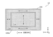
- FIG. 10A is a diagram illustrating a layout of sheet members 71a and 71b according to the fifth modification of the embodiment.
- the organic EL panel unit 10 shown in FIG. 10A has a sheet member 71b disposed in the peripheral region of the panel back surface 100a and a sheet member 71a disposed in an inner region inside the peripheral region of the panel back surface 100a.
- the sheet member 71b has a hole of a size and shape corresponding to the sheet member 71a, and the sheet member 71a is disposed at the position of the hole. That is, the sheet member 71b is disposed on the panel back surface 100a so as to surround the sheet member 71a.
- the layout of the sheet member 71a and the sheet member 71b in the present modification is such that the rectangular sheet member 71 is in the short side direction (X-axis direction) or the long side direction of the organic EL panel 100 (for example, as in the above embodiment).
- the layout is not simply arranged in the (Y-axis direction).
- sheet members 71a and 71b in this modification are arranged such that one part and the other part are adjacent to each other and the rolling directions are different from each other. This is common with the above embodiment.
- a sheet member 71b whose rolling direction is the Y-axis direction is disposed so as to surround the sheet member 71a whose rolling direction is the X-axis direction.
- the bending direction of the sheet member 71a in the central portion is the Y-axis direction and the bending direction of the sheet member 71b surrounding the sheet member 71a is the X-axis direction, they have a relationship of suppressing the bending.
- the sheet member 71a and the sheet member 71b cover almost the entire panel back surface 100a.
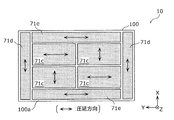
- FIG. 10B is a diagram illustrating a layout of the sheet members 71c, 71d, and 71e according to Modification 6 of the embodiment.
- the organic EL panel unit 10 shown in FIG. 10B has a plurality of sheet members 71d and 71e disposed in the peripheral region of the panel back surface 100a and a plurality of sheet members 71c disposed in the inner region of the panel back surface 100a.
- the layout of the plurality of sheet members 71c, 71d and 71e in the present modification is a layout obtained by subdividing the layout of the sheet members 71a and 71b in the modification 5 (see FIG. 10A).
- the sheet member 71d and the sheet member 71e adjacent to each other in the peripheral region are pasted on the peripheral region of the panel back surface 100a so that the rolling directions do not coincide with each other.
- each of the plurality of sheet members 71c is stuck to the inner region of the panel back surface 100a so that the rolling direction does not coincide with the adjacent sheet member 71c.
- each of the plurality of sheet members 71c in the inner region of the panel back surface 100a is suppressed by at least one adjacent sheet member 71c.
- the curbing suppression effect also occurs between the sheet member 71c in the inner region and the sheet member 71d or 71e in the peripheral region.
- one of the sheet members 71d and 71e adjacent to the sheet member 71c has a different rolling direction from the sheet member 71c. That is, the sheet member 71c and the sheet member 71d or 71e are placed in a relationship in which one suppresses the other curve.
- the rolling direction of the upper sheet member 71e coincides.
- the rolling direction of the sheet member 71c is not the same as that of the left sheet member 71d. Accordingly, the sheet member 71c and the sheet member 71d are placed in a relationship in which one suppresses the curvature of the other.
- the sheet member 71d is an example of the first sheet member
- one of the sheet members 71c and 71e is an example of the second sheet member
- the other is an example of the third sheet member.
- FIG. 10C is a diagram illustrating a layout of sheet members 71c and 71f according to Modification 7 of the embodiment.
- the organic EL panel unit 10 shown in FIG. 10C includes a plurality of sheet members 71f arranged in the peripheral region of the panel back surface 100a and a plurality of sheet members 71c arranged in an inner region inside the peripheral region of the panel back surface 100a. Have.
- the layout of the plurality of sheet members 71c and 71f in the present modification is a layout obtained by further subdividing the layout of the sheet members 71c, 71d, and 71e in the modification 6 (see FIG. 10B).
- each of the plurality of sheet members 71f is attached to the peripheral region of the panel back surface 100a so that the rolling direction does not coincide with the adjacent sheet member 71f.
- Each of the plurality of sheet members 71c is attached to the inner region of the panel back surface 100a so that the rolling direction does not coincide with the adjacent sheet member 71c.
- each of the plurality of sheet members 71f in the peripheral region of the panel back surface 100a is suppressed by at least one adjacent sheet member 71f. Further, the curvature of each of the plurality of sheet members 71c in the inner region of the panel back surface 100a is suppressed by at least one adjacent sheet member 71f.
- the curbing suppression effect also occurs between the sheet member 71c in the inner region and the sheet member 71f in the peripheral region. Specifically, when the sheet member 71c and the sheet member 71f are adjacent to each other and the rolling directions are different from each other, one of the sheet member 71c and the sheet member 71f is placed in a relationship that suppresses the other curve.
- the outer edge of the sheet member 71f disposed in the peripheral region of the panel back surface 100a is a portion where deformation due to temperature change is likely to occur because there is no other sheet member on the outer side.
- the number of sheet members 71f arranged in the peripheral region of the panel back surface 100a is increased (the size of each sheet member 71f is reduced), and the rolling directions of adjacent sheet members 71f are different from each other.
- the deformation amount of the outer edge of each sheet member 71f becomes relatively small, and as a result, the deformation of the edge of the organic EL panel 100 is suppressed.
- the organic EL panel unit 10 in Modification 7 shown in FIG. 10C is suppressed from being deformed as a whole (the maximum deformation amount is smaller) than the organic EL panel unit 10 in Modification 5 shown in FIG. 10A. Become).
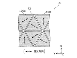
- FIG. 11 is a diagram illustrating a part of the layout of the plurality of sheet members 72 according to Modification Example 8 of the embodiment.
- the organic EL panel unit 10 shown in FIG. 11 has a plurality of triangular sheet members 72.
- Each of the plurality of sheet members 72 is affixed to the panel back surface 100a so that the rolling direction is different from that of the adjacent sheet members 72.
- the sheet member 72 is an equilateral triangle, and when attention is paid to a certain sheet member 72, there are three sheet members 72 arranged along each side. Further, the rolling direction of the one sheet member 72 and the rolling direction of the three sheet members 72 are shifted by 60 degrees (or 120 degrees).
- the bending direction of the one sheet member 72 and the respective bending directions of the three sheet members 72 are shifted by 60 degrees (or 120 degrees). For this reason, the one sheet member 72 and the three sheet members 72 are in a relationship of suppressing mutual curvature.
- the organic EL panel unit 10 it is possible to cover a wide area of the panel back surface 100a with a plurality of sheet members 72 by producing a plurality of one type of equilateral triangular sheet members 72.
- FIG. 12A is a diagram illustrating a layout of the sheet members 73a and 73b in the ninth modification of the embodiment.
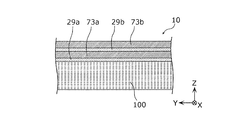
- FIG. 12B is a partial cross-sectional view of the organic EL panel unit 10 in Modification 9 of the embodiment.
- the sheet member 73a and the sheet member 73b are stacked in the thickness direction (Z-axis direction) of the organic EL panel 100, and the panel back surface 100a. Is attached.
- the sheet member 73a and the sheet member 73b are a first sheet member attached to the panel back surface 100a such that one part and the other part are adjacent to each other (in the Z-axis direction) and the rolling directions are different from each other. It is an example of the 2nd sheet member.
- the sheet member 73a is affixed to the panel back surface 100a by the adhesive member 29a, and the sheet member 73b is attached to the opposite side of the sheet back surface 100a of the sheet member 73a by the adhesive member 29b. Affixed to the surface. That is, the sheet member 73b is attached to the panel back surface 100a via the sheet member 73a.
- the sheet member 73a and the sheet member 73b are attached to the panel back surface 100a so that the rolling directions are different from each other.
- the sheet member 73a and the sheet member 73b are mutually connected because the curve direction of the sheet member 73a and the curve direction of the sheet member 73b intersect each other. It functions as a member that suppresses the bending of.
- the organic EL panel unit 10 in the present modification it is possible to improve the efficiency of heat dissipation for the organic EL panel 100 and to suppress the deformation of the organic EL panel 100 due to temperature changes.
- two sheet members (73a and 73b) are laminated on the panel back surface 100a, but three or more sheet members may be laminated.
- the size or shape of the plurality of sheet members may be different.
- the sheet member 73b may be attached to the panel back surface 100a by attaching at least a part of the sheet member 73b to the surface of the sheet member 73a opposite to the panel back surface 100a.
- the sheet member 73a is pasted so as to cover only a part of the panel back surface 100a.
- a part of the sheet member 73b may be attached to the surface of the sheet member 73a opposite to the panel back surface 100a, and the remaining part of the sheet member 73b may be directly attached to the panel back surface 100a.
- the sheet member 73b is attached to the surface of the sheet member 73a opposite to the panel back surface 100a, so that the sheet member 73a and the sheet member 73b are overlapped in the Z-axis direction (Z-axis direction). (Adjacent to) is formed.
- the deformation of the organic EL panel 100 is suppressed as compared with the case where the entire panel back surface 100a is covered only with the sheet member 73a, for example.
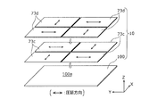
- FIG. 13 is a diagram illustrating a layout of the sheet members 73c and 73d according to Modification Example 10 of the embodiment.
- a plurality of sheet members are arranged in the thickness direction (Z-axis direction) of the organic EL panel 100, and also in a direction parallel to the panel back surface 100a.
- a plurality of sheet members are arranged.
- the organic EL panel unit 10 includes four sheet members 73c attached directly to the panel back surface 100a, and 4 attached to the panel back surface 100a via the four sheet members 73c. Sheet member 73d.
- each of the four sheet members 73c is arranged so that the rolling directions of the two adjacent sheet members 73c are different from each other, like the four sheet members 71 in the embodiment.
- the four sheet members 73d are arranged so that the rolling directions of the two adjacent sheet members 73d are different from each other.
- each of the four sheet members 73c is suppressed by at least one adjacent sheet member 73c.
- the curvature of each of the four sheet members 73d is suppressed by at least one adjacent sheet member 73d.
- each sheet member 73c is different from the rolling direction of the sheet member 73d stacked on the sheet member 73c (adjacent to the Z-axis direction).
- the pair of sheet members 73c and 73d stacked in the Z-axis direction are arranged so as to suppress the curvature of each other.
- the organic EL panel unit 10 in the present modification it is possible to improve the efficiency of heat dissipation for the organic EL panel 100 and to suppress the deformation of the organic EL panel 100 due to a temperature change.
- the organic EL panel unit 10 includes the organic EL panel 100 and a plurality of sheet members (71 and the like, the same applies hereinafter) attached to the back surface (panel back surface 100a) of the organic EL panel 100.
- these sheet members are arranged in a direction parallel to the panel back surface 100a or in a thickness direction of the organic EL panel 100.
- the material of the sheet member is aluminum
- the material of the sheet member is not limited to aluminum.
- a metal such as copper, stainless steel, or titanium may be employed.
- an aluminum alloy composed of aluminum, copper, or the like may be employed as a material for the sheet member.
- the sheet member 73a (see FIG. 12A) in the modified example 9 may be pasted on the panel back surface 100a, and further, the sheet member 71b (see FIG. 10A) in the modified example 5 may be stuck thereon.
- the sheet member 73a and the sheet member 71b adjacent in the thickness direction of the organic EL panel 100 function as members that suppress the mutual curvature. That is, the deformation of the organic EL panel 100 is suppressed.
- the sheet member 73a according to the modified example 9 is attached to the panel back surface 100a, and another sheet member is attached to the central region of the sheet member 73a. At this time, the other sheet member is stuck so that the rolling direction of the sheet member 73a is different from the rolling direction of the other sheet member.
- each of the plurality of sheet members are not limited to the shapes and layouts shown in the above embodiment and modifications 1 to 10.
- a plurality of sheet members having an outer shape formed by a curve or a combination of a curve and a straight line are combined to form the panel back surface 100a. It may be attached.
- the rolling direction of at least one sheet member may be different from the rolling direction of other sheet members adjacent to the sheet member.
- the present disclosure is useful for an organic EL display device that is required to be thin, for example, as an organic EL display device such as a television receiver, a monitor display, a digital signage, a portable terminal, a tablet terminal, or a table-type display device. And an organic EL panel unit included in the organic EL display device.
- an organic EL display device such as a television receiver, a monitor display, a digital signage, a portable terminal, a tablet terminal, or a table-type display device.
- an organic EL panel unit included in the organic EL display device included in the organic EL display device.
Landscapes
- Physics & Mathematics (AREA)
- Optics & Photonics (AREA)
- Electroluminescent Light Sources (AREA)
- Devices For Indicating Variable Information By Combining Individual Elements (AREA)
Abstract
Description
図2は、実施の形態における有機EL表示装置1の外観斜視図である。
図5は、実施の形態における有機ELパネル100の一部切り欠き斜視図である。
図8Aは、実施の形態における複数のシート部材71のレイアウトの一例を示す第1の図である。
以上のように、本実施の形態の有機EL表示装置1が備える有機ELパネルユニット10は、有機ELパネル100と、パネル背面100aに取り付けられた複数のシート部材71とを有する。
図9Aは、実施の形態の変形例1における複数のシート部材71のレイアウトを示す図である。
図9Bは、実施の形態の変形例2における複数のシート部材71のレイアウトを示す図である。
図9Cは、実施の形態の変形例3における複数のシート部材71のレイアウトを示す図である。
図9Dは、実施の形態の変形例4における複数のシート部材71のレイアウトを示す図である。
図10Aは、実施の形態の変形例5におけるシート部材71aおよび71bのレイアウトを示す図である。
図10Bは、実施の形態の変形例6におけるシート部材71c、71dおよび71eのレイアウトを示す図である。
図10Cは、実施の形態の変形例7におけるシート部材71cおよび71fのレイアウトを示す図である。
図11は、実施の形態の変形例8における複数のシート部材72のレイアウトの一部を示す図である。
図12Aは、実施の形態の変形例9におけるシート部材73aおよび73bのレイアウトを示す図である。
図13は、実施の形態の変形例10におけるシート部材73cおよび73dのレイアウトを示す図である。
以上のように、本出願において開示する技術の例示として、実施の形態および変形例を説明した。しかしながら、本開示における技術は、これらに限定されず、適宜、変更、置き換え、付加、省略などを行った実施の形態にも適用可能である。また、上記実施の形態および変形例で説明した各構成要素を組み合わせて、新たな実施の形態とすることも可能である。
10 有機ELパネルユニット
21 シャーシ
21a 凸部
29、29a、29b 接着部材
30 フレーム
40 バックカバー
50、51 回路基板
71、71a、71b、71c、71d、71e、71f、72、73a、73b、73c、73d シート部材
100 有機ELパネル
100a パネル背面
101 TFT基板
110 画素
110B、110G、110R サブ画素
111 バンク
120 画素回路
130 有機EL素子
131 陽極
132 EL層
133 陰極
140 ゲート配線
150 ソース配線
160 電源配線
Claims (7)
- 前面に画像を表示する有機ELパネルと、
前記有機ELパネルの背面であるパネル背面に取り付けられた複数のシート部材であって、金属板が圧延されることで形成された複数のシート部材とを備え、
前記複数のシート部材は、第一シート部材および第二シート部材を含み、
前記第一シート部材および前記第二シート部材は、一方の一部と他方の一部とが隣り合い、かつ、圧延方向が互いに異なるように前記パネル背面に取り付けられている
有機ELパネルユニット。 - 前記第一シート部材および前記第二シート部材は、前記パネル背面に平行な方向に並べられて、前記パネル背面に貼付されている
請求項1記載の有機ELパネルユニット。 - 前記複数のシート部材は、前記第一シート部材と重ならず、かつ、前記第二シート部材と隣り合う第三シート部材を含み、
前記第三シート部材は、前記第三シート部材の圧延方向が、前記第二シート部材または前記第一シート部材の圧延方向と異なるように前記パネル背面に貼付されている
請求項2記載の有機ELパネルユニット。 - 前記第二シート部材は、前記第一シート部材と前記第三シート部材との間に配置されており、
前記第三シート部材は、前記第三シート部材の圧延方向が、前記第二シート部材の圧延方向と異なるように前記パネル背面に貼付されている
請求項3記載の有機ELパネルユニット。 - 前記第一シート部材は、前記パネル背面の周縁領域に貼付されており、前記第二シート部材は、前記パネル背面の周縁領域より内側の内側領域に貼付されている
請求項1~4のいずれか1項に記載の有機ELパネルユニット。 - 前記第一シート部材は、前記パネル背面に貼付されており、
前記第二シート部材は、前記第二シート部材の少なくとも一部が、前記第一シート部材の、前記パネル背面とは反対側の面に貼付されていることで、前記パネル背面に取り付けられている
請求項1記載の有機ELパネルユニット。 - 請求項1~6のいずれか1項に記載の有機ELパネルユニットと、
前記有機ELパネルユニットの背面の少なくとも一部を覆うように配置されたバックカバーと、
を備える有機EL表示装置。
Priority Applications (2)
| Application Number | Priority Date | Filing Date | Title |
|---|---|---|---|
| JP2015554511A JP6213578B2 (ja) | 2013-12-27 | 2014-11-14 | 有機elパネルユニットおよび有機el表示装置 |
| US15/107,144 US9780339B2 (en) | 2013-12-27 | 2014-11-14 | Organic electroluminescent panel unit |
Applications Claiming Priority (2)
| Application Number | Priority Date | Filing Date | Title |
|---|---|---|---|
| JP2013273279 | 2013-12-27 | ||
| JP2013-273279 | 2013-12-27 |
Publications (1)
| Publication Number | Publication Date |
|---|---|
| WO2015097973A1 true WO2015097973A1 (ja) | 2015-07-02 |
Family
ID=53477888
Family Applications (1)
| Application Number | Title | Priority Date | Filing Date |
|---|---|---|---|
| PCT/JP2014/005731 Ceased WO2015097973A1 (ja) | 2013-12-27 | 2014-11-14 | 有機elパネルユニットおよび有機el表示装置 |
Country Status (3)
| Country | Link |
|---|---|
| US (1) | US9780339B2 (ja) |
| JP (1) | JP6213578B2 (ja) |
| WO (1) | WO2015097973A1 (ja) |
Families Citing this family (1)
| Publication number | Priority date | Publication date | Assignee | Title |
|---|---|---|---|---|
| JP6826376B2 (ja) * | 2016-04-28 | 2021-02-03 | エルジー ディスプレイ カンパニー リミテッド | 電気光学パネル |
Citations (3)
| Publication number | Priority date | Publication date | Assignee | Title |
|---|---|---|---|---|
| JPH1197587A (ja) * | 1997-09-16 | 1999-04-09 | Mitsubishi Electric Corp | 半導体装置 |
| WO2008013279A1 (en) * | 2006-07-28 | 2008-01-31 | Kyocera Corporation | Electronic component storing package and electronic device |
| JP2009272073A (ja) * | 2008-05-01 | 2009-11-19 | Seiko Epson Corp | 有機el装置及び電子機器 |
Family Cites Families (16)
| Publication number | Priority date | Publication date | Assignee | Title |
|---|---|---|---|---|
| JP2002123178A (ja) * | 2000-10-13 | 2002-04-26 | Matsushita Electric Ind Co Ltd | 映像表示装置 |
| JP2005148519A (ja) * | 2003-11-18 | 2005-06-09 | Konica Minolta Opto Inc | 偏光板及び表示装置 |
| JP4032353B2 (ja) * | 2003-12-26 | 2008-01-16 | セイコーエプソン株式会社 | 回路基板の製造方法、回路基板、電子機器、および電気光学装置 |
| JP3841306B2 (ja) * | 2004-08-05 | 2006-11-01 | 日東電工株式会社 | 位相差フィルムの製造方法 |
| US8446549B2 (en) * | 2005-11-29 | 2013-05-21 | Creator Technology B.V. | Color filter to prevent color errors in a roll up display |
| JP5108293B2 (ja) * | 2006-12-20 | 2012-12-26 | 富士フイルム株式会社 | 携帯機器及び撮像装置 |
| KR101540163B1 (ko) * | 2008-05-16 | 2015-07-28 | 신닛테츠스미킹 마테리알즈 가부시키가이샤 | 가요성 디스플레이용 스테인리스 강박 |
| JP5588626B2 (ja) * | 2008-08-04 | 2014-09-10 | 富士フイルム株式会社 | 光学フィルム、偏光板、光学補償フィルム、反射防止フィルムおよび液晶表示装置 |
| WO2010041227A1 (en) * | 2008-10-12 | 2010-04-15 | Barit, Efrat | Flexible devices and related methods of use |
| KR101789625B1 (ko) * | 2011-06-23 | 2017-10-25 | 엘지전자 주식회사 | 플렉서블 디스플레이를 구비하는 영상 표시 장치 및 그 제어방법 |
| JP5853311B2 (ja) | 2011-10-31 | 2016-02-09 | 株式会社Joled | 表示装置及び表示装置の製造方法 |
| KR101661526B1 (ko) * | 2012-04-08 | 2016-10-04 | 삼성전자주식회사 | 플렉서블 디스플레이 장치 및 그 ui 방법 |
| KR102104588B1 (ko) * | 2012-07-11 | 2020-04-24 | 삼성전자주식회사 | 플렉서블 디스플레이 장치 및 그 동작 방법 |
| KR102079348B1 (ko) * | 2012-07-30 | 2020-04-07 | 삼성전자주식회사 | 플렉서블 장치 및 그 동작 제어 방법 |
| KR102070244B1 (ko) * | 2012-08-01 | 2020-01-28 | 삼성전자주식회사 | 플렉서블 디스플레이 장치 및 그 제어 방법 |
| KR101892959B1 (ko) * | 2012-08-22 | 2018-08-29 | 삼성전자주식회사 | 플렉서블 디스플레이 장치 및 플렉서블 디스플레이 장치의 제어 방법 |
-
2014
- 2014-11-14 JP JP2015554511A patent/JP6213578B2/ja active Active
- 2014-11-14 US US15/107,144 patent/US9780339B2/en active Active
- 2014-11-14 WO PCT/JP2014/005731 patent/WO2015097973A1/ja not_active Ceased
Patent Citations (3)
| Publication number | Priority date | Publication date | Assignee | Title |
|---|---|---|---|---|
| JPH1197587A (ja) * | 1997-09-16 | 1999-04-09 | Mitsubishi Electric Corp | 半導体装置 |
| WO2008013279A1 (en) * | 2006-07-28 | 2008-01-31 | Kyocera Corporation | Electronic component storing package and electronic device |
| JP2009272073A (ja) * | 2008-05-01 | 2009-11-19 | Seiko Epson Corp | 有機el装置及び電子機器 |
Also Published As
| Publication number | Publication date |
|---|---|
| US20170033310A1 (en) | 2017-02-02 |
| US9780339B2 (en) | 2017-10-03 |
| JP6213578B2 (ja) | 2017-10-18 |
| JPWO2015097973A1 (ja) | 2017-03-23 |
Similar Documents
| Publication | Publication Date | Title |
|---|---|---|
| CN110021235B (zh) | 可折叠显示装置 | |
| US10845696B2 (en) | Display device | |
| US11452245B2 (en) | Display device | |
| US10930197B2 (en) | Display apparatus and tiled display apparatus | |
| US8049412B2 (en) | Organic light emitting display device | |
| JP6105911B2 (ja) | Oled表示パネル | |
| JP6219656B2 (ja) | 有機el表示装置 | |
| US20110109596A1 (en) | Flat display device with light shielding layer | |
| US20050236970A1 (en) | Self-emitting display | |
| CN105609529A (zh) | 窄边框大面积有机发光二极管显示器 | |
| TW201440582A (zh) | 可撓性顯示面板 | |
| KR20170057913A (ko) | 플렉서블 디스플레이 장치 | |
| JP4630535B2 (ja) | 表示装置の製造方法 | |
| JP6263747B2 (ja) | 画像表示装置および画像表示装置の製造方法 | |
| JP6076270B2 (ja) | ディスプレイ装置及びパネルユニット | |
| US20230112912A1 (en) | Display panel, display apparatus, method of preventing electro-magnetic interference in display panel, and method of fabricating display panel | |
| US11553604B2 (en) | Display apparatus | |
| US20220020956A1 (en) | Cover panel and display device comprising same | |
| JP2009301013A (ja) | 表示装置 | |
| US8076843B2 (en) | Organic electroluminescence display device | |
| US8941804B2 (en) | Liquid crystal display device | |
| WO2018173415A1 (ja) | 表示装置 | |
| JP6213578B2 (ja) | 有機elパネルユニットおよび有機el表示装置 | |
| TWI549283B (zh) | 有機發光二極體顯示器以及製造其之方法 | |
| JP2017096998A (ja) | 表示装置 |
Legal Events
| Date | Code | Title | Description |
|---|---|---|---|
| 121 | Ep: the epo has been informed by wipo that ep was designated in this application |
Ref document number: 14873447 Country of ref document: EP Kind code of ref document: A1 |
|
| ENP | Entry into the national phase |
Ref document number: 2015554511 Country of ref document: JP Kind code of ref document: A |
|
| WWE | Wipo information: entry into national phase |
Ref document number: 15107144 Country of ref document: US |
|
| NENP | Non-entry into the national phase |
Ref country code: DE |
|
| 122 | Ep: pct application non-entry in european phase |
Ref document number: 14873447 Country of ref document: EP Kind code of ref document: A1 |