WO2015087904A1 - ウェーハ加工方法 - Google Patents
ウェーハ加工方法 Download PDFInfo
- Publication number
- WO2015087904A1 WO2015087904A1 PCT/JP2014/082656 JP2014082656W WO2015087904A1 WO 2015087904 A1 WO2015087904 A1 WO 2015087904A1 JP 2014082656 W JP2014082656 W JP 2014082656W WO 2015087904 A1 WO2015087904 A1 WO 2015087904A1
- Authority
- WO
- WIPO (PCT)
- Prior art keywords
- wafer
- processing
- back surface
- device layer
- processing method
- Prior art date
- Legal status (The legal status is an assumption and is not a legal conclusion. Google has not performed a legal analysis and makes no representation as to the accuracy of the status listed.)
- Ceased
Links
Images







Classifications
-
- H—ELECTRICITY
- H10—SEMICONDUCTOR DEVICES; ELECTRIC SOLID-STATE DEVICES NOT OTHERWISE PROVIDED FOR
- H10P—GENERIC PROCESSES OR APPARATUS FOR THE MANUFACTURE OR TREATMENT OF DEVICES COVERED BY CLASS H10
- H10P54/00—Cutting or separating of wafers, substrates or parts of devices
-
- B—PERFORMING OPERATIONS; TRANSPORTING
- B23—MACHINE TOOLS; METAL-WORKING NOT OTHERWISE PROVIDED FOR
- B23K—SOLDERING OR UNSOLDERING; WELDING; CLADDING OR PLATING BY SOLDERING OR WELDING; CUTTING BY APPLYING HEAT LOCALLY, e.g. FLAME CUTTING; WORKING BY LASER BEAM
- B23K26/00—Working by laser beam, e.g. welding, cutting or boring
-
- B—PERFORMING OPERATIONS; TRANSPORTING
- B23—MACHINE TOOLS; METAL-WORKING NOT OTHERWISE PROVIDED FOR
- B23K—SOLDERING OR UNSOLDERING; WELDING; CLADDING OR PLATING BY SOLDERING OR WELDING; CUTTING BY APPLYING HEAT LOCALLY, e.g. FLAME CUTTING; WORKING BY LASER BEAM
- B23K26/00—Working by laser beam, e.g. welding, cutting or boring
- B23K26/36—Removing material
- B23K26/38—Removing material by boring or cutting
-
- B—PERFORMING OPERATIONS; TRANSPORTING
- B23—MACHINE TOOLS; METAL-WORKING NOT OTHERWISE PROVIDED FOR
- B23K—SOLDERING OR UNSOLDERING; WELDING; CLADDING OR PLATING BY SOLDERING OR WELDING; CUTTING BY APPLYING HEAT LOCALLY, e.g. FLAME CUTTING; WORKING BY LASER BEAM
- B23K26/00—Working by laser beam, e.g. welding, cutting or boring
- B23K26/36—Removing material
- B23K26/40—Removing material taking account of the properties of the material involved
- B23K26/402—Removing material taking account of the properties of the material involved involving non-metallic material, e.g. isolators
Definitions
- the present invention relates to a wafer processing method for dividing a wafer such as a semiconductor device or an electronic component into individual chips, and in particular, from a laminate in which an insulating film (for example, a low-k film) and a functional film are laminated on the surface of a semiconductor substrate.
- the present invention relates to a method for processing a wafer on which a device layer is formed.
- wafers with semiconductor devices or electronic parts formed on the surface are subjected to electrical tests in the probing process and then divided into individual chips (also called dies or pellets) in the dicing process.
- the individual chips are then die bonded to the component base in a die bonding process.
- wire bonding is performed, and after wire bonding, resin molding is performed to obtain a finished product such as a semiconductor device or an electronic component.
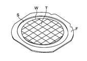
- the back surface of the wafer is attached to a dicing tape (also called a dicing sheet) S having a thickness of about 100 ⁇ m with an adhesive layer formed on one side, and a rigid ring shape. Is mounted on the frame F. In this state, the wafer W is transferred in the dicing process, between the dicing process and the die bonding process, and in the die bonding process.
- a dicing tape also called a dicing sheet
- a dicing apparatus that cuts the wafer by inserting a grinding groove into the wafer W with a thin grindstone called a dicing blade formed of fine diamond abrasive grains is used.
- the dicing blade is rotated at a high speed of 30,000 to 60,000 rpm and cut into the wafer W to completely cut the wafer W (full cut).
- the wafer W is cut into individual chips T, but the individual chips T are separated. In other words, since the arrangement of the chips T is not collapsed, the wafer state is maintained as a whole.
- dicing of a wafer having such a device layer is likely to cause film peeling and burrs, which is a big problem in the dicing process.
- the low-k film is very fragile. Therefore, when the device layer is cut by a dicing blade, there is a problem that the low-k film is easily peeled off. That is, if the low-k film is broken by cutting with a dicing blade, and the broken area spreads over the device formation area (chip formation area), the chip becomes a defective product, which reduces the yield of the semiconductor device to be manufactured. It will be a factor.
- a protective film is formed on the surface of a wafer on which a laminate (device layer) in which an insulating film and a functional film are laminated is formed.
- a protective film forming step is performed (step S100).
- a laser beam irradiation process is performed in which the laser beam is irradiated on the surface of the wafer through the protective film (step S102).
- the laser beam is reciprocated along the streets, so that a laser processing groove having a width wider than the width of the dicing blade (cutting blade) along the streets is formed on the laminated body forming the streets of the wafer. Is formed.
- a protective film removing process for removing the protective film coated on the surface of the wafer is performed (step S104).
- a dicing process (cutting process) is performed in which the wafer is cut with a dicing blade along the laser processing groove formed on the street of the wafer (step S106).
- the cutting groove which reaches a back surface is formed in the wafer along the laser processing groove formed in the street.
- the wafer is cut along the laser processing grooves formed in the streets and divided into individual chips. In this dicing process, only the semiconductor substrate (silicon substrate or the like) is cut by the dicing blade.
- Patent Document 1 requires a laser processing apparatus (laser scriber) in addition to the dicing apparatus. Further, in the laser irradiation process, in order to form a laser processing groove wider than the width of the dicing blade, it is necessary to perform laser beam irradiation by reciprocating along one street. For this reason, there is a problem that productivity is poor and the cost is increased.
- laser processing apparatus laser scriber
- the present invention has been made in view of such circumstances, and an object thereof is to provide a wafer processing method that can divide a wafer into individual chips with good processing quality while improving productivity and reducing costs. To do.
- a wafer processing method is a wafer in which a plurality of chips are formed in a region defined by division lines in a device layer formed on the surface of a semiconductor substrate. Is divided into individual chips along the planned dividing line, and the laser beam guided by the liquid beam is irradiated along the planned dividing line from the surface side on which the device layer of the wafer is formed. And a groove forming step for removing the device layer in the division line and forming a groove in the semiconductor substrate, and a back surface processing step for reducing the thickness of the wafer by processing the back surface of the wafer.
- the device layer in the planned dividing line is removed and the groove is formed in the semiconductor substrate. Therefore, even if a protective film is not formed on the surface of the wafer, thermal damage and contamination during processing can be prevented, yield can be improved, and reliability can be improved. Further, a dicing process such as dicing with a dicing blade or laser dicing is not required. Therefore, the wafer can be divided into individual chips with good processing quality while improving productivity and reducing costs.
- the back surface processing step processes the back surface of the wafer until the groove is exposed on the back surface of the wafer.
- the wafer is divided into individual chips by the back surface processing step. Therefore, it is not necessary to perform the expanding step after the back surface processing step is performed, and the productivity can be further improved.
- the back surface processing step ends the processing of the back surface of the wafer before the grooves are exposed on the back surface of the wafer, and the back surface processing step is performed.
- the groove formed on the wafer at the time of back surface processing is not exposed on the back surface of the wafer, it is possible to eliminate the risk of a chemical solution or the like used at the time of back surface processing entering the surface (device surface) of the wafer via the groove. .
- the wafer is a wafer including a low-k film in a device layer.
- the wafer is a wafer containing GaN (gallium nitride) in the device layer.
- the fourth aspect and the fifth aspect are one of the preferable aspects from the viewpoint that the effect of the present invention becomes more remarkable. That is, even when the device layer formed on the surface of the semiconductor substrate contains a low-k film or GaN (gallium nitride), the wafer can be divided into individual chips without causing film peeling or burrs. Therefore, the yield can be improved and the reliability can be improved.
- GaN gallium nitride
- the liquid beam is made of an alkaline aqueous solution.
- a groove with a high aspect ratio can be formed, and the processing rate is improved.
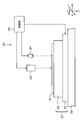
- the flowchart which shows the flow of the wafer processing method which concerns on one Embodiment of this invention.
- Schematic showing the configuration of the laser processing equipment Sectional view showing an example of wafer Configuration diagram showing the configuration of the laser processing section Schematic showing how the wafer is irradiated with water-guided laser light
- Schematic showing how wafer backside processing is performed
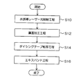
- the flowchart which shows the flow of the wafer processing method which concerns on other embodiment of this invention.
- FIG. 1 is a flowchart showing a flow of a wafer processing method according to an embodiment of the present invention.
- a water-guided laser light irradiation process (corresponding to the “groove forming process” of the present invention) for irradiating the surface of the wafer W with water-guided laser light is performed (step S10).
- This water-guided laser light irradiation step is performed using a laser processing apparatus 20 shown in FIG.
- the laser processing apparatus 20 shown in FIG. 2 mainly includes a wafer moving unit 22 that moves the wafer W, an observation optical unit 24 that observes the surface of the wafer W, a laser processing unit 26 that laser processes the wafer W, and laser processing. It is comprised from the control part 28 which controls each part of the apparatus 20.
- FIG. 2 mainly includes a wafer moving unit 22 that moves the wafer W, an observation optical unit 24 that observes the surface of the wafer W, a laser processing unit 26 that laser processes the wafer W, and laser processing. It is comprised from the control part 28 which controls each part of the apparatus 20.
- FIG. 3 is a cross-sectional view showing an example of the wafer W.
- a wafer W shown in FIG. 3 is composed of a semiconductor substrate 10 such as silicon, and a device layer 12 is formed on a surface 10 a of the semiconductor substrate 10.
- the device layer 12 is formed of a stacked body in which a low-k film and a functional film that forms a circuit are stacked.
- the wafer W is divided into a plurality of areas by the division lines 14 arranged in a lattice pattern, and various devices constituting a semiconductor chip are formed in each of the divided areas. It is assumed that such a wafer W is supplied to the laser processing apparatus 20.
- the wafer moving unit 22 includes a suction stage 30 that sucks and holds the wafer W, and an XYZ ⁇ table 32 provided on the main body base 34.
- the suction stage 30 has a pump (not shown), and a plurality of suction holes are provided on the surface.
- the suction stage 30 sucks and holds the wafer W through the suction holes by operating a pump.
- the XYZ ⁇ table 32 includes guide rails (not shown) and is controlled by the control unit 28 to move in four directions of XYZ ⁇ .
- the three directions of XYZ are orthogonal to each other, among which the X direction and the Y direction are horizontal directions, and the Z direction is a vertical direction.
- the ⁇ direction is a rotation direction with a vertical axis (Z axis) as a rotation axis.
- the observation optical unit 24 is provided so as to face the wafer W sucked and held on the suction stage 30 and includes an illumination device (not shown) and a CCD (Charge Coupled Device) camera (not shown).
- the observation optical unit 24 images the surface of the wafer W by irradiating the wafer W with illumination light according to an instruction from the control unit 28 and converting the reflected light from the wafer W into an electrical signal using a CCD camera. Get the data. This imaging data is sent to the control unit 28 and used for alignment of the wafer W.
- the laser processing unit 26 irradiates the surface of the wafer W with water-induced laser light in accordance with instructions from the control unit 28.
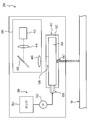
- FIG. 4 is a configuration diagram showing the configuration of the laser processing unit 26.
- the laser processing unit 26 includes a laser light supply unit 36, a liquid supply unit 38, and a processing head 40.
- the laser light supply unit 36 includes a laser light source 42, and the laser light oscillated from the laser light source 42 is collected inside the processing head 40 through an optical system such as a collimator lens 44, a mirror 46, and a condenser lens 48. Lighted.
- the liquid supply unit 38 includes a tank 50 that stores liquid (water in this example) and a pump 52, and the liquid pressurized by the pump 52 (pressurized liquid) is supplied to the processing head 40.
- the processing head 40 includes a liquid chamber 54 that temporarily stores the liquid supplied from the liquid supply unit 38, a liquid inlet 56 for introducing the liquid supplied from the liquid supply unit 38 into the liquid chamber 54, and a laser.
- a window portion 58 that guides laser light supplied from the light supply portion 36 to the inside of the machining head 40 and a nozzle 60 that forms a liquid injection port are provided.
- the window 58 is provided on the upper surface (the surface opposite to the wafer W side) of the head main body 62 that is the main body of the processing head 40, and is a light that can transmit the laser light supplied from the laser light supply unit 36. Constructed from a permeable material.
- the light transmissive material for example, glass, quartz, sapphire, transparent plastic (for example, acrylic resin, hard vinyl chloride, etc.) can be used.
- the laser light supplied from the laser light supply unit 36 passes through the window part 58 in the liquid chamber 54 formed inside the processing head 40 (head main body 62) (specifically, the inlet part of the nozzle 60). ).
- the nozzle 60 is formed of a minute hole provided in the lower surface (the surface on the wafer W side) of the head main body 62 and is disposed at a position facing the window portion 58 with the liquid chamber 54 interposed therebetween. That is, the nozzle 60 is disposed on the optical axis of the laser beam guided from the laser beam supply unit 36 through the window 58 to the inside of the liquid chamber 54, and the ejection direction of the liquid ejected from the nozzle 60 and the laser beam.
- the optical axes of the light coincide.
- the laser light guided from the laser light supply unit 36 through the window 58 to the inside of the liquid chamber 54 is totally reflected from the inside of the beam-like liquid (liquid beam) irradiated from the nozzle 60 while being reflected on the wafer W.
- the surface of the wafer W is irradiated.
- laser light that is guided along the liquid beam ejection direction while repeating total reflection inside the liquid beam is referred to as “water-guided laser light”.
- the wafer W is placed on the suction stage 30 of the laser processing apparatus 20 with the surface of the wafer W (the surface on which the device layer 12 is formed) facing upward.
- the wafer W is sucked and held.
- the wafer W is aligned from the surface by the illumination device of the observation optical unit 24 and the CCD camera.
- the alignment method is performed by an alignment method using image processing. Since an alignment method using image processing is generally well known, description thereof is omitted.
- the XYZ ⁇ table 32 moves in the XY direction, and a beam-like liquid (liquid beam) is directed from the nozzle 60 of the processing head 40 toward the wafer W along the planned division line formed on the surface of the wafer W. ) Is injected.
- the laser light introduced from the laser light supply unit 36 into the liquid chamber 54 inside the processing head 40 (head main body 62) through the window 58 is entirely inside the liquid beam ejected from the nozzle 60.
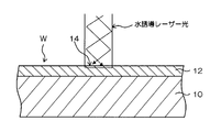
- the light is guided toward the wafer W while repeating the reflection, and is irradiated to the position where the division line 14 is formed on the surface of the wafer W as shown in FIG.
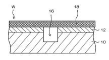
- the device layer 12 in the division line 14 is removed without causing film peeling, burrs, or the like, and the semiconductor substrate 10 of the wafer W extends along the division line 14.
- a processing groove 16 having a predetermined depth is formed.
- a high-pressure liquid water jet
- the water-guided laser light that is, the planned division line 14
- debris generated during laser processing is used. This debris does not adhere to the periphery of the processing area even if processing scraps referred to as are generated.
- the wafer W as the workpiece can be cooled while removing the substance melted by the water-induced laser light from the processing position to avoid contamination. Therefore, even if a protective film is not formed on the surface of the wafer W, thermal damage and contamination during processing can be effectively prevented, yield can be improved, and reliability can be improved.
- the laser beam irradiation range can be easily controlled by the liquid beam ejection width (beam diameter), and for example, a processing groove can be formed with a width of about 30 ⁇ m. Therefore, it is not necessary to perform a plurality of times of processing in one division line, the number of processing feeds of the wafer W is reduced, and it is possible to form a high-quality processed groove 16 with high productivity.
- the laser processing conditions in the water-guided laser light irradiation step are set as follows, for example.
- UV light source UV (ultraviolet light) -pulse laser Wavelength: 400 nm or less Repeat frequency: 1 to 100 kHz Average output: 0.5-10W Processing feed rate: 10 to 1000 mm / s
- a UV light source is preferably used as the laser light source.
- Light in the ultraviolet region (UV light) irradiated from the UV light source has a high absorption rate by the metal, and the metal removal performance is improved. Therefore, even when a metal film such as TEG (Test Element Group) is formed on the division line 14, the metal film can be efficiently removed by irradiation with water-guided laser light.
- TEG Transmission Element Group
- the aspect which the liquid beam injected from the nozzle 60 of the process head 40 consists of water was shown, not only this but the aspect which consists of silicon oil, alkaline aqueous solution etc., for example is preferably employ
- the processing groove 16 having a high aspect ratio can be formed compared to the aspect in which the liquid beam is made of water, and the processing rate can be improved. .
- BG back grind
- a back surface processing step is performed in which the back surface of the wafer W is processed to reduce the thickness of the wafer W (step S12).
- the wafer W with the protective tape 18 attached to the front surface is adsorbed to the rotating adsorption table 72 of the back grinder device 70 with the protective tape 18 facing downward, and the back surface is removed. It is ground with a rotating grindstone 74 ((A) part in FIG. 8) and processed to a predetermined thickness (400 ⁇ m or less). Next, it is polished by a polishing head (not shown) while being held on the suction table 72, and the work-affected layer formed during grinding is removed (part (B) in FIG. 8). Since the protective tape 18 has sufficient hardness against the grinding pressure, it can be processed with high accuracy.
- the thickness of the wafer W after such a back surface processing step is performed so that the processing groove 16 formed in the wafer W in the water-guided laser light irradiation step in step S10 is exposed (exposed) on the back surface of the wafer W. Is done. As a result, the wafer W is divided into individual chips.
- the water-guided laser light is divided along the planned division line 14 from the surface side of the wafer W on which the device layer 12 is formed on the surface of the semiconductor substrate 10 in the water-guided laser light irradiation step. Irradiate.
- the device layer 12 in the planned dividing line 14 can be removed without causing film peeling or burrs, and the processed groove 16 having a predetermined depth can be formed in the semiconductor substrate 10. For this reason, even if a protective film is not formed on the surface of the wafer W, thermal damage and contamination during processing can be prevented, yield can be improved, and reliability can be improved.
- the wafer W can be divided into individual chips with good processing quality while improving productivity and reducing costs.
- the back surface processing process is performed to reduce the thickness of the wafer W by processing the back surface of the wafer W, so that chipping and cracking occur. Therefore, an extremely thin chip having a good end face shape can be manufactured.
- the present invention is not limited to this.
- a wafer including GaN (gallium nitride) in the device layer 12 The same effect can be obtained also when processing.
- FIG. 9 is an explanatory diagram showing a flow of a wafer processing method according to another embodiment of the present invention.
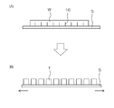
- FIG. 10 is a schematic view showing a state in which the back surface processing step is performed.
- FIG. 11 is a schematic diagram illustrating how the expanding process is performed. 9 to 11, elements that are the same as or similar to those shown so far are assigned the same reference numerals, and descriptions thereof are omitted.
- the back surface processing is terminated immediately before the processing groove 16 formed in the wafer W is exposed on the back surface of the wafer W (step S12).
- a dicing tape transfer step is performed in which a dicing tape S having an adhesive on one side is applied to the back surface of the wafer W, and then the protective tape 18 attached to the front surface of the wafer W is peeled off. Performed (step S14). As a result, the dicing tape S is attached to the back surface of the wafer W as shown in FIG.
- the wafer W can be divided into individual chips T by applying tension to the dicing tape S and stretching it.
- the tension is smaller than when the expanding process is performed with the dicing tape S attached to the surface of the wafer W.
- the wafer W can be divided into individual chips T.
- SYMBOLS 10 Semiconductor substrate, 12 ... Device layer, 14 ... Dividing line, 16 ... Processing groove, 18 ... Protection tape, 20 ... Laser processing apparatus, 22 ... Wafer moving part, 24 ... Observation optical part, 26 ... Laser processing part, DESCRIPTION OF SYMBOLS 28 ... Control part, 30 ... Adsorption stage, 32 ... XYZ (theta) table, 36 ... Laser light supply part, 38 ... Liquid supply part, 40 ... Processing head, 42 ... Laser light source, 50 ... Tank, 52 ... Pump, 54 ... Liquid chamber 56 ... Liquid inlet, 58 ... Window, 60 ... Nozzle, F ... Frame, S ... Dicing sheet, T ... Chip, W ... Wafer
Landscapes
- Engineering & Computer Science (AREA)
- Physics & Mathematics (AREA)
- Optics & Photonics (AREA)
- Plasma & Fusion (AREA)
- Mechanical Engineering (AREA)
- Dicing (AREA)
- Laser Beam Processing (AREA)
- Mechanical Treatment Of Semiconductor (AREA)
Abstract
生産性の向上及びコストダウンを図りつつ、良好な加工品質でウェーハを個々のチップに分割できるウェーハ加工方法を提供する。本発明のウェーハ加工方法は、半導体基板(10)の表面に形成されたデバイス層(12)に複数のチップが分割予定ライン(14)によって区画された領域に形成されているウェーハ(W)を、分割予定ラインに沿って個々のチップに分割する方法であって、ウェーハのデバイス層が形成される表面側から、液体ビームによって誘導されたレーザー光を分割予定ラインに沿って照射することにより、分割予定ラインにおけるデバイス層を除去するとともに半導体基板に溝(16)を形成する溝形成工程と、ウェーハの裏面を加工して、ウェーハの厚さを薄くする裏面加工工程と、を含む。
Description
本発明は、半導体装置や電子部品等のウェーハを個々のチップに分割するウェーハ加工方法に関し、特に、半導体基板の表面に絶縁膜(例えばLow-k膜)及び機能膜が積層された積層体からなるデバイス層が形成されたウェーハの加工方法に関する。
半導体製造工程等において、表面に半導体装置や電子部品等が形成されたウェーハは、プロービング工程で電気試験が行われた後、ダイシング工程で個々のチップ(ダイ、又はペレットとも言われる)に分割され、次に個々のチップはダイボンディング工程で部品基台にダイボンディングされる。ダイボンディングされた後はワイヤボンディングされ、ワイヤボンディングされた後は、樹脂モールドされて、半導体装置や電子部品等の完成品となる。
プロービング工程の後ウェーハは、図13に示すように、片面に粘着層が形成された厚さ100μm程度のダイシングテープ(ダイシングシートとも称される)Sに裏面を貼り付けられ、剛性のあるリング状のフレームFにマウントされる。ウェーハWはこの状態でダイシング工程内、ダイシング工程-ダイボンディング工程間、及びダイボンディング工程内を搬送される。
ダイシング工程では、微細なダイヤモンド砥粒で形成されたダイシングブレードと呼ばれる薄型砥石でウェーハWに研削溝を入れてウェーハをカットするダイシング装置が用いられている。
ダイシング装置では、このダイシングブレードを30,000~60,000rpmで高速回転させてウェーハWに切込み、ウェーハWを完全切断(フルカット)する。このときウェーハWの裏面に貼られたダイシングテープSは、表面から10μm程度しか切り込まれていないので、ウェーハWは個々のチップTに切断されてはいるものの、個々のチップTがバラバラにはならず、チップT同士の配列が崩れていないので全体としてウェーハ状態が保たれている。
近年、IC、LSI等のデバイスの高集積化、小型化に伴い、シリコン等の半導体基板の表面に、SiOF、BSG(SiOB)等の無機物系の膜やポリイミド系、パリレン系(パリレンは登録商標)等のポリマー膜である有機物系の膜からなる低誘電率絶縁体被膜(Low-k膜)と回路を形成する機能膜とが積層された積層体からなるデバイス層が形成されたウェーハが実用化されている。
しかし、このようなデバイス層のあるウェーハのダイシングは、膜剥がれやバリ等が発生しやすく、ダイシング工程における大きな問題となっている。特に、デバイス層にLow-k膜が含まれる場合、Low-k膜は非常に脆いことから、ダイシングブレードによる切断が行われると、Low-k膜に剥離が生じやすい問題がある。すなわち、ダイシングブレードによって切断すると、Low-k膜が破壊され、この破壊された領域がデバイス形成領域(チップ形成領域)に広がると、チップは不良品となり、製造される半導体装置の歩留りを低下させてしまう要因となる。
上記問題を解消するために、ダイシングブレードによる切断に先立って、ストリートと称される分割予定ラインに沿ってレーザー加工溝を形成してデバイス層を分断した後に、ダイシングブレードによって切断を行う方法が提案されている(例えば、特許文献1参照)。
特許文献1に記載された方法は、図14に示すように、最初に、表面に絶縁膜及び機能膜が積層された積層体(デバイス層)が形成されたウェーハの表面に保護膜を形成する保護膜形成工程が行われる(ステップS100)。次に、ウェーハの表面に、保護膜を通してレーザー光を照射するレーザー光照射工程が行われる(ステップS102)。このレーザー光照射工程では、ストリートに沿ってレーザー光を往復移動させることにより、ウェーハのストリートを形成する積層体には、ストリートに沿ってダイシングブレード(切削ブレード)の幅より広い幅のレーザー加工溝が形成される。
レーザー光照射工程が実施された後、ウェーハの表面に被覆された保護膜を除去する保護膜除去工程が行われる(ステップS104)。次に、ウェーハのストリートに形成されたレーザー加工溝に沿ってダイシングブレードでウェーハを切削するダイシング工程(切削工程)が行われる(ステップS106)。これにより、ウェーハは、ストリートに形成されたレーザー加工溝に沿って裏面に達する切削溝が形成される。この結果、ウェーハはストリートに形成されたレーザー加工溝に沿って切断され、個々のチップに分割される。このダイシング工程においてはダイシングブレードによって半導体基板(シリコン基板等)だけが切断されることになる。
しかしながら、特許文献1に記載された方法では、ダイシング装置のほかにレーザー加工装置(レーザースクライバ)が必要である。また、レーザー照射工程では、ダイシングブレードの幅より広いレーザー加工溝を形成するために、レーザー光の照射を1つのストリートに沿って往復移動して行わなければならない。このため、生産性が悪く、コストアップを招く問題がある。
また、特許文献1に記載された方法では、加工時の熱ダメージやコンタミネーションを防ぐため、レーザー光照射工程が実施される前にウェーハの表面に保護膜を形成する必要があり、保護膜にかかるコストも問題となっている。
本発明は、このような事情に鑑みてなされたもので、生産性の向上及びコストダウンを図りつつ、良好な加工品質でウェーハを個々のチップに分割できるウェーハ加工方法を提供することを目的とする。
上記目的を達成するために、本発明の第1態様に係るウェーハ加工方法は、半導体基板の表面に形成されたデバイス層に複数のチップが分割予定ラインによって区画された領域に形成されているウェーハを、分割予定ラインに沿って個々のチップに分割する方法であって、ウェーハのデバイス層が形成される表面側から、液体ビームによって誘導されたレーザー光を分割予定ラインに沿って照射することにより、分割予定ラインにおけるデバイス層を除去するとともに半導体基板に溝を形成する溝形成工程と、ウェーハの裏面を加工して、ウェーハの厚さを薄くする裏面加工工程と、を含む。
本態様によれば、溝形成工程においてウェーハの表面側から液体ビームによって誘導されたレーザー光を分割予定ラインに沿って照射することにより、分割予定ラインにおけるデバイス層を除去するとともに半導体基板に溝を形成するので、ウェーハの表面に保護膜を形成しなくても、加工時の熱ダメージやコンタミネーションを防ぐことができ、歩留りの向上を実現して信頼性を向上させることができる。また、ダイシングブレードによるダイシングやレーザーダイシング等のダイシング工程が不要となる。したがって、生産性の向上及びコストダウンを図りつつ、良好な加工品質でウェーハを個々のチップに分割できる。
本発明の第2態様に係るウェーハ加工方法は、第1態様において、裏面加工工程は、溝がウェーハの裏面に露出するまでウェーハの裏面を加工する。
本態様によれば、裏面加工工程によってウェーハは個々のチップに分割される。したがって、裏面加工工程が行われた後にエキスパンド工程を行う必要がなく、更なる生産性の向上を図ることができる。
本発明の第3態様に係るウェーハ加工方法は、第1態様において、裏面加工工程は、溝がウェーハの裏面に露出する前にウェーハの裏面の加工を終了し、裏面加工工程が行われたウェーハの表面又は裏面にダイシングテープを貼付するダイシングテープ貼付工程と、ダイシングテープに張力を加えて、個々のチップ間隔を拡大するエキスパンド工程と、をさらに含む。
本態様によれば、裏面加工時にウェーハに形成された溝はウェーハの裏面に露出しないので、裏面加工時に使用する薬液等がウェーハの表面(デバイス面)に溝を介して回り込む危険性を排除できる。
本発明の第4態様に係るウェーハ加工方法は、第1態様~第3態様のいずれかにおいて、ウェーハは、デバイス層にLow-k膜が含まれるウェーハである。
本発明の第5態様に係るウェーハ加工方法は、第1態様~第3態様のいずれかにおいて、ウェーハは、デバイス層にGaN(窒化ガリウム)が含まれるウェーハである。
第4態様及び第5態様は、本発明の効果がより顕著となる観点から好ましい態様の1つである。すなわち、半導体基板の表面に形成されるデバイス層にLow-k膜やGaN(窒化ガリウム)が含まれる場合でも、膜剥がれやバリ等が発生することなく、ウェーハを個々のチップに分割することができるので、歩留りの向上を実現して信頼性を向上させることができる。
本発明の第6態様に係るウェーハ加工方法は、第1態様~第5態様のいずれかにおいて、液体ビームは、アルカリ水溶液からなる。
本態様によれば、高アスペクト比の溝を形成することができ、加工レートが向上する。
本発明によれば、生産性の向上及びコストダウンを図りつつ、良好な加工品質でウェーハを個々のチップに分割できる。
以下、添付図面に従って本発明の好ましい実施形態について説明する。
図1は、本発明の一実施形態に係るウェーハ加工方法の流れを示すフローチャートである。
<水誘導レーザー光照射工程>
まず、ウェーハWの表面に水誘導レーザー光を照射する水誘導レーザー光照射工程(本発明の「溝形成工程」に相当)が行われる(ステップS10)。この水誘導レーザー光照射工程は、図2に示すレーザー加工装置20を用いて実施される。
まず、ウェーハWの表面に水誘導レーザー光を照射する水誘導レーザー光照射工程(本発明の「溝形成工程」に相当)が行われる(ステップS10)。この水誘導レーザー光照射工程は、図2に示すレーザー加工装置20を用いて実施される。
図2に示すレーザー加工装置20は、主として、ウェーハWを移動させるウェーハ移動部22と、ウェーハWの表面を観察する観察光学部24と、ウェーハWをレーザー加工するレーザー加工部26と、レーザー加工装置20の各部を制御する制御部28とから構成されている。
図3は、ウェーハWの一例を示す断面図である。図3に示すウェーハWは、シリコン等の半導体基板10からなり、半導体基板10の表面10aにはデバイス層12が形成されている。デバイス層12は、Low-k膜と、回路を形成する機能膜とが積層された積層体により形成される。ウェーハWは、格子状に配列された分割予定ライン14によって複数の領域に区画され、この区画された各領域に半導体チップを構成する各種デバイスが形成されている。レーザー加工装置20には、このようなウェーハWが供給されるものとする。
ウェーハ移動部22は、ウェーハWを吸着保持する吸着ステージ30と、本体ベース34上に設けられたXYZθテーブル32とを有する。
吸着ステージ30は、不図示のポンプを有するとともに、複数の吸着穴が表面に設けられている。吸着ステージ30は、ポンプを作動させることにより、吸着穴を介してウェーハWを吸着保持する。
XYZθテーブル32は、不図示のガイドレールを備え、制御部28に制御されて、XYZθの4方向に移動する。なお、図2に示す例では、XYZの3方向は互いに直交し、このうちX方向およびY方向は水平方向であり、Z方向は鉛直方向である。またθ方向は、鉛直方向軸(Z軸)を回転軸とする回転方向である。
観察光学部24は、吸着ステージ30に吸着保持されたウェーハWに対向するように設けられ、図示しない照明装置及び図示しないCCD(Charge Coupled Device)カメラを有する。観察光学部24は、制御部28の指示に従って、ウェーハWに照明光を照明装置により照射して、ウェーハWからの反射光をCCDカメラにより電気信号に変換することで、ウェーハWの表面の撮像データを得る。この撮像データは制御部28に送られて、ウェーハWのアライメントに用いられる。
レーザー加工部26は、制御部28の指示に従って、ウェーハWの表面に水誘導レーザー光を照射する。
図4は、レーザー加工部26の構成を示す構成図である。同図に示すように、レーザー加工部26は、レーザー光供給部36、液体供給部38、及び加工ヘッド40を備えている。
レーザー光供給部36は、レーザー光源42を備えており、レーザー光源42から発振されたレーザー光は、コリメートレンズ44、ミラー46、集光レンズ48等の光学系を経て加工ヘッド40の内部に集光される。
液体供給部38は、液体(本例では水)を貯留するタンク50及びポンプ52を備えており、ポンプ52により加圧された液体(加圧液体)が加工ヘッド40に供給される。
加工ヘッド40は、液体供給部38から供給された液体を一時的に収容する液体チャンバー54と、液体供給部38から供給された液体を液体チャンバー54に導入するための液体導入口56と、レーザー光供給部36から供給されたレーザー光を加工ヘッド40の内部に導く窓部58と、液体の噴射口を形成するノズル60とを備えている。
窓部58は、加工ヘッド40の本体であるヘッド本体62の上面(ウェーハW側とは反対側の面)に設けられており、レーザー光供給部36から供給されたレーザー光を透過可能な光透過性材料から構成される。光透過性材料としては、例えば、ガラス、石英、サファイア、透明プラスチック(例えば、アクリル樹脂、硬質塩化ビニールなど)を用いることができる。これにより、レーザー光供給部36から供給されたレーザー光は、窓部58を介して加工ヘッド40(ヘッド本体62)の内部に形成される液体チャンバー54内(具体的にはノズル60の入口部)に導かれる。
ノズル60は、ヘッド本体62の下面(ウェーハW側の面)に設けられた微小孔からなり、液体チャンバー54を挟んで窓部58と対向する位置に配置される。すなわち、ノズル60は、レーザー光供給部36から窓部58を介して液体チャンバー54の内部に導かれるレーザー光の光軸上に配置されており、ノズル60から噴射される液体の噴射方向とレーザー光の光軸は一致している。これにより、レーザー光供給部36から窓部58を介して液体チャンバー54の内部に導かれるレーザー光は、ノズル60から照射されるビーム状の液体(液体ビーム)の内部を全反射しながらウェーハWに向かって誘導され、ウェーハWの表面に照射される。なお、本明細書では、液体ビームの内部を、全反射を繰り返しながら液体ビームの噴射方向に沿って誘導されるレーザー光を「水誘導レーザー光」と称する。
次に、上述の如く構成されるレーザー加工装置20を用いて実施する水誘導レーザー光照射工程について説明する。
この水誘導レーザー光照射工程では、まず、レーザー加工装置20の吸着ステージ30上にウェーハWの表面(デバイス層12が形成された側の面)を上向きにして載置し、吸着ステージ30上にウェーハWを吸着保持する。
この状態でウェーハWは、観察光学部24の照明装置とCCDカメラによって表面からアライメントされる。アライメント方法は画像処理を用いたアライメント方法で行われる。なお、画像処理を用いたアライメント方法は一般的によく知られているので、説明は省略する。
アライメントが終了すると、XYZθテーブル32がXY方向に移動して、ウェーハWの表面に形成された分割予定ラインに沿って、加工ヘッド40のノズル60からウェーハWに向かってビーム状の液体(液体ビーム)が噴射される。このとき、レーザー光供給部36から窓部58を介して加工ヘッド40(ヘッド本体62)の内部の液体チャンバー54内に導入されたレーザー光は、ノズル60から噴射される液体ビームの内部で全反射を繰り返しながらウェーハWに向かって誘導され、図5に示すように、ウェーハWの表面の分割予定ライン14が形成される位置に照射される。これにより、図6に示すように、膜剥がれやバリ等が発生することなく、分割予定ライン14におけるデバイス層12が除去されるとともに、ウェーハWの半導体基板10には、分割予定ライン14に沿って所定深さの加工溝16が形成される。
このように本実施形態では、水誘導レーザー光が照射されるウェーハWの加工位置(すなわち分割予定ライン14)には常に高圧の液体(ウォータージェット)が供給されるので、レーザー加工時に発生するデブリと称される加工屑が発生しても、このデブリが加工領域周辺に付着することもない。また、水誘導レーザー光によって溶融した物質を加工位置から取り除き汚染を避けると同時に被加工物としてのウェーハWを冷却することができる。したがって、ウェーハWの表面に保護膜を形成しなくても、加工時の熱ダメージやコンタミネーションを効果的に防ぐことができ、歩留りの向上を実現して信頼性を向上させることができる。
また、本実施形態では、液体ビームの噴射幅(ビーム径)によってレーザー光の照射範囲を容易に制御することが可能であり、例えば30μm程度の幅で加工溝を形成することができる。したがって、1つの分割ラインにおいて複数回の加工が不要となり、ウェーハWの加工送り回数が減少され、生産性のよい高品質な加工溝16を形成することが可能となる。
なお、本実施形態では、水誘導レーザー光照射工程におけるレーザー加工条件として、例えば以下のように設定される。
光源 :UV(紫外線)-パルスレーザー
波長 :400nm以下
繰り返し周波数 :1~100kHz
平均出力 :0.5~10W
加工送り速度 :10~1000mm/s
このように本実施形態では、レーザー光源として、UV光源が好ましく用いられる。UV光源から照射される紫外線領域の光(UV光)は金属による吸収率が高く、金属除去性能が向上する。したがって、分割予定ライン14上にTEG(Test Element Group)等の金属膜が形成されている場合でも、水誘導レーザー光の照射により金属膜を効率的に除去することができる。
波長 :400nm以下
繰り返し周波数 :1~100kHz
平均出力 :0.5~10W
加工送り速度 :10~1000mm/s
このように本実施形態では、レーザー光源として、UV光源が好ましく用いられる。UV光源から照射される紫外線領域の光(UV光)は金属による吸収率が高く、金属除去性能が向上する。したがって、分割予定ライン14上にTEG(Test Element Group)等の金属膜が形成されている場合でも、水誘導レーザー光の照射により金属膜を効率的に除去することができる。
また、本実施形態では、加工ヘッド40のノズル60から噴射される液体ビームが水からなる態様を示したが、これに限らず、例えばシリコンオイル、アルカリ水溶液等からなる態様も好ましく採用することができる。特に、液体ビームがアルカリ水溶液からなる態様によれば、液体ビームが水からなる態様に比べて、高アスペクト比の加工溝16を形成することができ、加工レートの向上を図ることが可能となる。
<裏面加工工程>
次に、ウェーハWの表面に形成されたデバイス層12を保護するために、片面に粘着剤を有する保護テープ(BG(バックグラインド)テープ)18をウェーハWの表面に貼付した後(図7参照)、ウェーハWの裏面を加工して、ウェーハWの厚さを薄くする裏面加工工程が行われる(ステップS12)。
次に、ウェーハWの表面に形成されたデバイス層12を保護するために、片面に粘着剤を有する保護テープ(BG(バックグラインド)テープ)18をウェーハWの表面に貼付した後(図7参照)、ウェーハWの裏面を加工して、ウェーハWの厚さを薄くする裏面加工工程が行われる(ステップS12)。
この裏面加工工程では、表面に保護テープ18が貼付されたウェーハWは、図8に示すように、バックグラインダ装置70の回転する吸着テーブル72に保護テープ18側を下向きにして吸着され、裏面を回転する砥石74で研削され(図8の(A)部)、所定の厚さ(400μm以下)に加工される。次いで吸着テーブル72に保持されたまま図示しない研磨ヘッドによって研磨されて、研削加工時に形成された加工変質層が除去される(図8の(B)部)。保護テープ18は研削加工圧に対して十分な硬度を有しているので、精度よく加工することができる。
このような裏面加工工程が行われた後のウェーハWの厚さは、ステップS10の水誘導レーザー光照射工程でウェーハWに形成された加工溝16がウェーハWの裏面に露出(表出)するまで行われる。これにより、ウェーハWは個々のチップに分割される。
以上のように、本実施形態によれば、水誘導レーザー光照射工程において半導体基板10の表面にデバイス層12が形成されたウェーハWの表面側から水誘導レーザー光を分割予定ライン14に沿って照射する。これにより、膜剥がれやバリ等が発生することなく、分割予定ライン14におけるデバイス層12を除去できるとともに、半導体基板10に所定深さの加工溝16を形成することができる。このため、ウェーハWの表面に保護膜を形成しなくても、加工時の熱ダメージやコンタミネーションを防ぐことができ、歩留りの向上を実現して信頼性を向上させることができる。また、ダイシングブレードによるダイシングやレーザーダイシング(ステルスダイシングとも称される)等のダイシング工程が不要となるので、生産性の向上を図ることが可能となる。したがって、生産性の向上及びコストダウンを図りつつ、良好な加工品質でウェーハWを個々のチップに分割できる。
さらに本実施形態では、水誘導レーザー光照射工程が行われた後に、ウェーハWの裏面を加工して、ウェーハWの厚さを薄くする裏面加工工程が行われるので、チッピングや割れかけが生じることがなく、端面形状が良好な極薄のチップを製造することができる。
なお、本実施形態では、ウェーハWとして、デバイス層12にLow-k膜を含むウェーハを加工する場合について説明したが、これに限らず、例えば、デバイス層12にGaN(窒化ガリウム)を含むウェーハを加工する場合についても同様の効果を得ることができる。
次に、本発明の他の実施形態について説明する。図9は、本発明の他の実施形態に係るウェーハ加工方法の流れを示す説明図である。図10は、裏面加工工程が行われる様子を示す概略図である。図11は、エキスパンド工程が行われる様子を示す概略図である。図9~図11において、これまで示した図と共通又は類似する要素には同一の符号を付し、その説明を省略する。
図9に示すウェーハ加工方法では、裏面加工工程において、図10に示すように、ウェーハWに形成された加工溝16がウェーハWの裏面に露出する直前で裏面加工を終了する(ステップS12)。
上記の裏面加工工程が行われた後、片面に粘着剤を有するダイシングテープSをウェーハWの裏面に貼付した後、ウェーハWの表面に貼付されている保護テープ18を剥離するダイシングテープ転写工程が行われる(ステップS14)。これにより、図11の(A)部に示すように、ウェーハWの裏面にダイシングテープSが貼付された状態となる。
次に、図11の(B)部に示すように、ウェーハWの裏面に貼り付けられたダイシングテープSに張力を加えて引き伸ばすことにより、ウェーハWの各チップ間の間隔を拡大するエキスパンド工程が行われる(ステップS16)。これにより、ウェーハWを個々のチップTに分割することができる。
このウェーハ加工方法によれば、裏面加工工程においてウェーハWに形成される加工溝16はウェーハWの裏面に露出しないので、裏面加工時に使用する薬液がウェーハWの表面(デバイス面)へ回り込む危険性を排除できる。
なお、ダイシングテープ転写工程において、転写回数は増えるが、図12の(A)部に示すように、ウェーハWの表面にダイシングテープSを貼付するようにしてもよい。その後、エキスパンド工程において、図12の(B)部に示すように、ダイシングテープSに張力を加えて引き伸ばすことにより、ウェーハWを個々のチップTに分割することができる。この態様によれば、ウェーハWにはダイシングテープS側に加工溝16が形成されるので、ウェーハWの表面にダイシングテープSが貼付された状態でエキスパンド工程を行う場合に比べて、より小さな張力でウェーハWを個々のチップTに分割することが可能となる。
以上、本発明の実施形態について説明したが、本発明は、以上の例には限定されず、本発明の要旨を逸脱しない範囲において、各種の改良や変形を行ってもよいのはもちろんである。
10…半導体基板、12…デバイス層、14…分割予定ライン、16…加工溝、18…保護テープ、20…レーザー加工装置、22…ウェーハ移動部、24…観察光学部、26…レーザー加工部、28…制御部、30…吸着ステージ、32…XYZθテーブル、36…レーザー光供給部、38…液体供給部、40…加工ヘッド、42…レーザー光源、50…タンク、52…ポンプ、54…液体チャンバー、56…液体導入口、58…窓部、60…ノズル、F…フレーム、S…ダイシングシート、T…チップ、W…ウェーハ
Claims (6)
- 半導体基板の表面に形成されたデバイス層に複数のチップが分割予定ラインによって区画された領域に形成されているウェーハを、前記分割予定ラインに沿って個々のチップに分割する方法であって、
前記ウェーハの前記デバイス層が形成される表面側から、液体ビームによって誘導されたレーザー光を前記分割予定ラインに沿って照射することにより、前記分割予定ラインにおける前記デバイス層を除去するとともに前記半導体基板に溝を形成する溝形成工程と、
前記ウェーハの裏面を加工して、前記ウェーハの厚さを薄くする裏面加工工程と、
を含むウェーハ加工方法。 - 前記裏面加工工程は、前記溝が前記ウェーハの裏面に露出するまで前記ウェーハの裏面を加工する請求項1に記載のウェーハ加工方法。
- 前記裏面加工工程は、前記溝が前記ウェーハの裏面に露出する前に前記ウェーハの裏面の加工を終了し、
前記裏面加工工程が行われた前記ウェーハの表面又は裏面にダイシングテープを貼付するダイシングテープ貼付工程と、
前記ダイシングテープに張力を加えて、個々のチップ間隔を拡大するエキスパンド工程と、
をさらに含む請求項1に記載のウェーハ加工方法。 - 前記ウェーハは、前記デバイス層にLow-k膜が含まれるウェーハである請求項1~3のいずれか1項に記載のウェーハ加工方法。
- 前記ウェーハは、前記デバイス層にGaNが含まれるウェーハである請求項1~3のいずれか1項に記載のウェーハ加工方法。
- 前記液体ビームは、アルカリ水溶液からなる請求項1~5のいずれか1項に記載のウェーハ加工方法。
Applications Claiming Priority (2)
| Application Number | Priority Date | Filing Date | Title |
|---|---|---|---|
| JP2013-258288 | 2013-12-13 | ||
| JP2013258288A JP2015115538A (ja) | 2013-12-13 | 2013-12-13 | ウェーハ加工方法 |
Publications (1)
| Publication Number | Publication Date |
|---|---|
| WO2015087904A1 true WO2015087904A1 (ja) | 2015-06-18 |
Family
ID=53371205
Family Applications (1)
| Application Number | Title | Priority Date | Filing Date |
|---|---|---|---|
| PCT/JP2014/082656 Ceased WO2015087904A1 (ja) | 2013-12-13 | 2014-12-10 | ウェーハ加工方法 |
Country Status (2)
| Country | Link |
|---|---|
| JP (1) | JP2015115538A (ja) |
| WO (1) | WO2015087904A1 (ja) |
Cited By (6)
| Publication number | Priority date | Publication date | Assignee | Title |
|---|---|---|---|---|
| EP3460836A1 (en) * | 2017-09-20 | 2019-03-27 | Kabushiki Kaisha Toshiba | Semiconductor device manufacturing apparatus and semiconductor device manufacturing method |
| CN112490190A (zh) * | 2019-09-12 | 2021-03-12 | 株式会社迪思科 | 晶片的加工方法 |
| CN112885720A (zh) * | 2021-01-14 | 2021-06-01 | 江西译码半导体有限公司 | 一种晶圆切割方法 |
| CN118024128A (zh) * | 2024-03-28 | 2024-05-14 | 安徽长飞先进半导体有限公司 | 晶圆平坦化装置及方法 |
| US20240174559A1 (en) * | 2022-11-24 | 2024-05-30 | Samsung Display Co., Ltd. | Processing apparatus and processing method |
| WO2025033382A1 (ja) * | 2023-08-08 | 2025-02-13 | 国立大学法人 東京大学 | SiCウェハのダイシング方法及びその装置 |
Families Citing this family (3)
| Publication number | Priority date | Publication date | Assignee | Title |
|---|---|---|---|---|
| CN110087820B (zh) | 2016-12-22 | 2021-12-24 | 三菱电机株式会社 | 激光加工装置、激光加工方法及半导体装置的制造方法 |
| JP7083573B2 (ja) * | 2018-04-09 | 2022-06-13 | 株式会社ディスコ | ウェーハの加工方法 |
| JP7083572B2 (ja) * | 2018-04-09 | 2022-06-13 | 株式会社ディスコ | ウェーハの加工方法 |
Citations (6)
| Publication number | Priority date | Publication date | Assignee | Title |
|---|---|---|---|---|
| JP2008153349A (ja) * | 2006-12-15 | 2008-07-03 | Disco Abrasive Syst Ltd | ウェーハの分割方法 |
| JP2011056514A (ja) * | 2009-09-07 | 2011-03-24 | Kaneka Corp | 光電変換素子の製造方法 |
| JP2011091239A (ja) * | 2009-10-23 | 2011-05-06 | Disco Abrasive Syst Ltd | 半導体デバイスの製造方法 |
| JP2011101062A (ja) * | 2011-02-21 | 2011-05-19 | Canon Inc | 薄膜半導体装置の製造方法 |
| JP2012004478A (ja) * | 2010-06-21 | 2012-01-05 | Disco Abrasive Syst Ltd | 加工装置 |
| JP2013125961A (ja) * | 2011-12-14 | 2013-06-24 | Semileds Optoelectronics Co Ltd | 垂直発光ダイオードチップ及びその製造方法 |
-
2013
- 2013-12-13 JP JP2013258288A patent/JP2015115538A/ja active Pending
-
2014
- 2014-12-10 WO PCT/JP2014/082656 patent/WO2015087904A1/ja not_active Ceased
Patent Citations (6)
| Publication number | Priority date | Publication date | Assignee | Title |
|---|---|---|---|---|
| JP2008153349A (ja) * | 2006-12-15 | 2008-07-03 | Disco Abrasive Syst Ltd | ウェーハの分割方法 |
| JP2011056514A (ja) * | 2009-09-07 | 2011-03-24 | Kaneka Corp | 光電変換素子の製造方法 |
| JP2011091239A (ja) * | 2009-10-23 | 2011-05-06 | Disco Abrasive Syst Ltd | 半導体デバイスの製造方法 |
| JP2012004478A (ja) * | 2010-06-21 | 2012-01-05 | Disco Abrasive Syst Ltd | 加工装置 |
| JP2011101062A (ja) * | 2011-02-21 | 2011-05-19 | Canon Inc | 薄膜半導体装置の製造方法 |
| JP2013125961A (ja) * | 2011-12-14 | 2013-06-24 | Semileds Optoelectronics Co Ltd | 垂直発光ダイオードチップ及びその製造方法 |
Cited By (8)
| Publication number | Priority date | Publication date | Assignee | Title |
|---|---|---|---|---|
| EP3460836A1 (en) * | 2017-09-20 | 2019-03-27 | Kabushiki Kaisha Toshiba | Semiconductor device manufacturing apparatus and semiconductor device manufacturing method |
| CN112490190A (zh) * | 2019-09-12 | 2021-03-12 | 株式会社迪思科 | 晶片的加工方法 |
| CN112490190B (zh) * | 2019-09-12 | 2026-03-27 | 株式会社迪思科 | 晶片的加工方法 |
| CN112885720A (zh) * | 2021-01-14 | 2021-06-01 | 江西译码半导体有限公司 | 一种晶圆切割方法 |
| US20240174559A1 (en) * | 2022-11-24 | 2024-05-30 | Samsung Display Co., Ltd. | Processing apparatus and processing method |
| US12577152B2 (en) * | 2022-11-24 | 2026-03-17 | Samsung Display Co., Ltd. | Processing apparatus and processing method |
| WO2025033382A1 (ja) * | 2023-08-08 | 2025-02-13 | 国立大学法人 東京大学 | SiCウェハのダイシング方法及びその装置 |
| CN118024128A (zh) * | 2024-03-28 | 2024-05-14 | 安徽长飞先进半导体有限公司 | 晶圆平坦化装置及方法 |
Also Published As
| Publication number | Publication date |
|---|---|
| JP2015115538A (ja) | 2015-06-22 |
Similar Documents
| Publication | Publication Date | Title |
|---|---|---|
| WO2015087904A1 (ja) | ウェーハ加工方法 | |
| KR102419485B1 (ko) | 웨이퍼의 박화 방법 | |
| KR102369760B1 (ko) | 웨이퍼의 가공 방법 | |
| KR102384101B1 (ko) | 웨이퍼의 박화 방법 | |
| KR102368338B1 (ko) | 웨이퍼의 가공 방법 | |
| KR102163441B1 (ko) | 웨이퍼의 가공 방법 | |
| CN100459054C (zh) | 晶片加工方法 | |
| US11114342B2 (en) | Wafer processing method | |
| KR20170055909A (ko) | SiC 기판의 분리 방법 | |
| JPWO2004100240A1 (ja) | 板状部材の分割方法及び分割装置 | |
| CN103715082A (zh) | 晶片的加工方法 | |
| US11056346B2 (en) | Wafer processing method | |
| KR20200014195A (ko) | 칩 제조 방법 | |
| JP2014099522A (ja) | 板状物の加工方法 | |
| JP5863264B2 (ja) | ウエーハの加工方法 | |
| KR20190143393A (ko) | 피가공물의 가공 방법 | |
| JP7693336B2 (ja) | ウェーハの製造方法、チップの製造方法、ウェーハ及びレーザービームの位置合わせ方法 | |
| KR102948553B1 (ko) | 디바이스 칩의 제조 방법 | |
| KR102914272B1 (ko) | 웨이퍼의 가공 방법 | |
| JP2013021209A (ja) | ウエーハの加工方法 | |
| JP2024034584A (ja) | 積層ウェーハの分割方法 | |
| JP2023172142A (ja) | チップの製造方法 | |
| JP2023056101A (ja) | デバイスチップの製造方法 |
Legal Events
| Date | Code | Title | Description |
|---|---|---|---|
| 121 | Ep: the epo has been informed by wipo that ep was designated in this application |
Ref document number: 14869663 Country of ref document: EP Kind code of ref document: A1 |
|
| NENP | Non-entry into the national phase |
Ref country code: DE |
|
| 122 | Ep: pct application non-entry in european phase |
Ref document number: 14869663 Country of ref document: EP Kind code of ref document: A1 |