WO2015083738A1 - 封止機能付導通材、電気モジュール、電気モジュールの製造方法 - Google Patents
封止機能付導通材、電気モジュール、電気モジュールの製造方法 Download PDFInfo
- Publication number
- WO2015083738A1 WO2015083738A1 PCT/JP2014/081973 JP2014081973W WO2015083738A1 WO 2015083738 A1 WO2015083738 A1 WO 2015083738A1 JP 2014081973 W JP2014081973 W JP 2014081973W WO 2015083738 A1 WO2015083738 A1 WO 2015083738A1
- Authority
- WO
- WIPO (PCT)
- Prior art keywords
- conductive material
- sealing
- electrode
- sealing function
- solid
- Prior art date
- Legal status (The legal status is an assumption and is not a legal conclusion. Google has not performed a legal analysis and makes no representation as to the accuracy of the status listed.)
- Ceased
Links
Images



Classifications
-
- H—ELECTRICITY
- H01—ELECTRIC ELEMENTS
- H01G—CAPACITORS; CAPACITORS, RECTIFIERS, DETECTORS, SWITCHING DEVICES, LIGHT-SENSITIVE OR TEMPERATURE-SENSITIVE DEVICES OF THE ELECTROLYTIC TYPE
- H01G9/00—Electrolytic capacitors, rectifiers, detectors, switching devices, light-sensitive or temperature-sensitive devices; Processes of their manufacture
- H01G9/20—Light-sensitive devices
- H01G9/2068—Panels or arrays of photoelectrochemical cells, e.g. photovoltaic modules based on photoelectrochemical cells
- H01G9/2077—Sealing arrangements, e.g. to prevent the leakage of the electrolyte
-
- H—ELECTRICITY
- H01—ELECTRIC ELEMENTS
- H01G—CAPACITORS; CAPACITORS, RECTIFIERS, DETECTORS, SWITCHING DEVICES, LIGHT-SENSITIVE OR TEMPERATURE-SENSITIVE DEVICES OF THE ELECTROLYTIC TYPE
- H01G9/00—Electrolytic capacitors, rectifiers, detectors, switching devices, light-sensitive or temperature-sensitive devices; Processes of their manufacture
- H01G9/20—Light-sensitive devices
- H01G9/2027—Light-sensitive devices comprising an oxide semiconductor electrode
- H01G9/2031—Light-sensitive devices comprising an oxide semiconductor electrode comprising titanium oxide, e.g. TiO2
-
- H—ELECTRICITY
- H01—ELECTRIC ELEMENTS
- H01G—CAPACITORS; CAPACITORS, RECTIFIERS, DETECTORS, SWITCHING DEVICES, LIGHT-SENSITIVE OR TEMPERATURE-SENSITIVE DEVICES OF THE ELECTROLYTIC TYPE
- H01G9/00—Electrolytic capacitors, rectifiers, detectors, switching devices, light-sensitive or temperature-sensitive devices; Processes of their manufacture
- H01G9/20—Light-sensitive devices
- H01G9/2059—Light-sensitive devices comprising an organic dye as the active light absorbing material, e.g. adsorbed on an electrode or dissolved in solution
-
- Y—GENERAL TAGGING OF NEW TECHNOLOGICAL DEVELOPMENTS; GENERAL TAGGING OF CROSS-SECTIONAL TECHNOLOGIES SPANNING OVER SEVERAL SECTIONS OF THE IPC; TECHNICAL SUBJECTS COVERED BY FORMER USPC CROSS-REFERENCE ART COLLECTIONS [XRACs] AND DIGESTS
- Y02—TECHNOLOGIES OR APPLICATIONS FOR MITIGATION OR ADAPTATION AGAINST CLIMATE CHANGE
- Y02E—REDUCTION OF GREENHOUSE GAS [GHG] EMISSIONS, RELATED TO ENERGY GENERATION, TRANSMISSION OR DISTRIBUTION
- Y02E10/00—Energy generation through renewable energy sources
- Y02E10/50—Photovoltaic [PV] energy
- Y02E10/542—Dye sensitized solar cells
-
- Y—GENERAL TAGGING OF NEW TECHNOLOGICAL DEVELOPMENTS; GENERAL TAGGING OF CROSS-SECTIONAL TECHNOLOGIES SPANNING OVER SEVERAL SECTIONS OF THE IPC; TECHNICAL SUBJECTS COVERED BY FORMER USPC CROSS-REFERENCE ART COLLECTIONS [XRACs] AND DIGESTS
- Y02—TECHNOLOGIES OR APPLICATIONS FOR MITIGATION OR ADAPTATION AGAINST CLIMATE CHANGE
- Y02P—CLIMATE CHANGE MITIGATION TECHNOLOGIES IN THE PRODUCTION OR PROCESSING OF GOODS
- Y02P70/00—Climate change mitigation technologies in the production process for final industrial or consumer products
- Y02P70/50—Manufacturing or production processes characterised by the final manufactured product
Definitions
- the present invention relates to a conductive material with a sealing function, an electric module, and a method for manufacturing the electric module.
- Examples of the electric module having the above structure include a dye-sensitized solar cell module in which dye-sensitized solar cell elements each including a transparent electrode and a counter electrode are provided in the same plane.
- an electric module is disclosed in which the counter electrode of the first element is also present in the gap between the elements and is directly connected to the transparent electrode of the second element ( Patent Document 1).
- a photoelectric conversion module in which photoelectric conversion elements including a transparent electrode, a counter electrode, and a sealing insulating portion that seals and insulates them are provided in the same plane, adjacent photoelectric conversion elements are To electrically connect, a part of the transparent electrode member of the first photoelectric conversion element and a part of the counter electrode member of the second photoelectric conversion element face each other, and a conductive material is provided therebetween.
- a photoelectric conversion module having a series structure between a plurality of cells is disclosed (see Patent Document 2).
- the present invention has been made in view of the above circumstances, and collectively includes a conductive material for electrically connecting a pair of opposed electrodes and a sealing material for bonding and sealing these electrodes. It is an object of the present invention to provide a conductive material with a sealing function that can be disposed in a manner, an electric module using the conductive material, and a method for manufacturing the electric module.
- a conductive material with a sealing function in which a solid conductive material is directly held by a sealing material [2] The conductive material with a sealing function according to [1], wherein the solid conductive material and the sealing material are integrated. [3] The conductive material with a sealing function according to [2], wherein the solid conductive material is one type selected from a conductive wire, a conductive tube, and a conductive mesh. [4] The sealing material has a sealing function according to [2] or [3], wherein a cross-sectional shape perpendicular to the longitudinal direction is a substantially circular shape (reel shape) or a substantially square shape (ribbon shape). Conductive material.
- a method for manufacturing an electric module comprising: a first electrode provided on a first base material; and a second electrode provided on a second base material, wherein the [1] ] Through the conductive material with a sealing function according to any one of [6] to [6], the step A for disposing the first electrode and the second electrode opposite to each other, and the solid conductive material, A step B in which the first electrode and the second electrode are in direct contact with each other, and the sealing material is in close contact with the solid conductive material without gaps, and in close contact with the first electrode and the second electrode. And a method of manufacturing an electrical module.
- the conductive material with a sealing function is disposed between the first electrode and the second electrode.
- the manufacturing method of the electrical module of description [11] The method for manufacturing an electric module according to [9] or [10], wherein the conductive material with a sealing function prepared in a separate process in advance is used. [12] In the above [9] or [10], the conductive material with a sealing function is produced as the process A and the process B progress, and the conductive material with a sealing function is supplied to the process A.
- the manufacturing method of the electrical module of description is described.
- An electrical module in which a plurality of first electrodes provided on a first substrate and a plurality of second electrodes provided on a second substrate are arranged to face each other, 1] to [4]
- the electric material which is divided into a plurality of cells and is electrically connected to the first electrode and the second electrode of the cells adjacent to each other by the conductive material with a sealing function described in any one of [1] to [4]
- a module is given as an example of a preferred embodiment (see FIGS. 2 and 3).
- a method for manufacturing an electric module comprising a plurality of first electrodes provided on a first base material and a plurality of second electrodes provided on a second base material, Through the conductive material with a sealing function according to any one of [1] to [4], the plurality of first electrodes and the plurality of second electrodes are opposed to each other so that a plurality of cells are formed.
- Arranging step A and the solid conductive material are brought into direct contact with the first electrode of one of the cells adjacent to each other and the second electrode of the other cell;
- An example of a preferred embodiment is a method for manufacturing an electrical module that includes the step B of bringing the conductive material into close contact with the first electrode and the second electrode (see FIGS. 2 and 3).
- the solid conducting material and the sealing material are integrated, the conducting material for electrically connecting a pair of opposing electrodes and the sealing for bonding and sealing these electrodes
- the material can be disposed in a lump. Therefore, the solid conductive material and the sealing material can be easily arranged at predetermined positions. Furthermore, the ratio which a space
- Embodiments of a conductive material with a sealing function, an electric module, and a method for manufacturing an electric module according to the present invention will be described.
- this Embodiment demonstrates the meaning of invention concretely, and does not limit this invention.
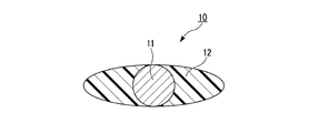
- FIG. 1A is a schematic cross-sectional view showing an example of a conductive material with a sealing function of the present embodiment.
- the conductive material 10 with a sealing function of the present embodiment covers the solid conductive material 11 disposed in the center and having a circular cross-sectional shape perpendicular to the longitudinal direction, and the outer periphery of the solid conductive material 11.
- a sealing material 12 having an elliptical cross-sectional shape perpendicular to the longitudinal direction.
- the centers of the solid conducting material 11 and the sealing material 12 are at the same position.
- the upper end and the lower end of the circular solid conductive material 11 are in contact with the upper end and the lower end of the oval sealing material 12.
- the solid conducting material 11 and the sealing material 12 are integrated. There is a void between the solid conducting material 11 and the sealing material 12. It means a state where both are in close contact with each other without being present.
- both of the conductive materials with a sealing function 10 are in close contact with each other, but some may be in close contact and the other may be in non-contact.
- the diameter when the opening is assumed to be a circle having the same area is preferably 0.2 mm or less, and the number is 100 / mm 2.
- the diameter of the gap is more preferably 0.1 mm or less, and further preferably 0.05 mm or less.
- the number of voids is more preferably 40 pieces / mm 2 or less, and further preferably 12 pieces / mm 2 or less. More preferably, the diameter of the gap is 0.15 mm or less, and the number of the gaps is 40 / mm 2 or less.
- both the cross-sectional shapes of the solid conductive material 11 and the sealing material 12 are the same. It may be substantially circular.
- the solid conducting material 11 is not particularly limited as long as it is a member capable of electrically conducting electrodes formed on two opposing substrates.
- the electrical module having a plurality of cells formed between the two base materials is a conductive member that electrically connects adjacent cells to each other.
- the electrical module is a dye-sensitized solar cell module including a plurality of cells each including a transparent electrode and a counter electrode
- the solid conductive material 11 includes one counter electrode and the other of the cells adjacent to each other. It is a conductive member for electrically connecting the transparent electrode.
- the solid conductive material 11 for example, one type selected from a conductive wire, a conductive tube, a conductive foil, a conductive plate, and a conductive mesh is used.
- the material of the solid conductive material 11 include metals such as gold, silver, copper, chromium, titanium, platinum, nickel, tungsten, iron, and aluminum, or alloys of two or more of these metals. There is no particular limitation.
- the material include a resin composition such as polyurethane and polytetrafluoroethylene (PTFE) in which conductive fine particles (for example, fine particles of the metal or alloy, fine particles of carbon black) are dispersed.
- PTFE polytetrafluoroethylene
- the shape of the cross section perpendicular to the longitudinal direction of the conducting wire is not particularly limited, but for example, a substantially circular shape such as a circular shape or an elliptical shape, or a substantially polygonal shape such as a square shape, a rectangular shape, a trapezoidal shape, or a star shape, etc. Can be mentioned.
- the size (for example, diameter) of the cross section perpendicular to the longitudinal direction of the conducting wire is not particularly limited, and the cell aperture ratio required between the electrical modules to which the conductive material 10 with a sealing function is applied, and between the electrodes. It is set as appropriate according to the interval and the like.
- vertical to the longitudinal direction of a conductive tube is not specifically limited, For example, circular shape, elliptical shape, square shape, rectangular shape, polygonal shape, star shape, etc. are mentioned.
- the shape of the outer periphery and the inner periphery may be different.
- the size (for example, diameter) of the cross section perpendicular to the longitudinal direction of the conductive tube is not particularly limited, and the cell aperture ratio required between the electrical modules to which the conductive material 10 with a sealing function is applied and the distance between the electrodes. It sets suitably according to etc.
- the width and thickness of the conductive foil, the conductive plate, and the conductive mesh are not particularly limited, depending on the cell aperture ratio, the spacing between the electrodes, and the like required for the electric module to which the conductive material 10 with a sealing function is applied. Is set as appropriate.
- the sealing material 12 is not particularly limited as long as it is a non-conductive member that can bond two opposing substrates and seal an electric module formed between the two substrates.
- the electric module having a plurality of cells formed between the two base materials as an example of the sealing material 12
- it is a member that electrically insulates cells adjacent to each other.
- the electrical module is a dye-sensitized solar cell module including a plurality of cells each including a transparent electrode and a counter electrode
- the sealing material 12 separates and seals adjacent cells and is adjacent to each other. This is a member for preventing an unintended electrical short circuit between the cells to be performed.
- the material of the sealing material 12 is temporarily fluid, such as a hot melt adhesive (thermoplastic resin), a thermosetting resin, an ultraviolet curable resin, an ultraviolet curable resin and a resin containing a thermosetting resin. And a resin material that is solidified by an appropriate treatment.
- a hot melt adhesive thermoplastic resin
- thermosetting resin examples include an epoxy resin, a polyimide resin, a benzoxazone resin, and the like.
- an ultraviolet curable resin what contains photopolymerizable monomers, such as an acrylic ester and a methacrylic ester, is mentioned, for example.
- the shape of the cross section perpendicular to the longitudinal direction of the sealing material 12 is not particularly limited, but is preferably approximately circular (reel) or approximately square (ribbon).
- the substantially circular shape means that the shape of the cross section perpendicular to the longitudinal direction of the sealing material 12 is a shape having no corners, for example, a circular shape or an elliptical shape.
- the substantially square shape means that the shape of the cross section perpendicular to the longitudinal direction of the sealing material 12 is a polygon, for example, a triangle, a square, or a rectangle.
- the substantially square shape includes a case where the sealing material 12 has a flat plate shape (strip shape).
- the “substantially” of the substantially square shape means that the portion corresponding to the corner of the polygon may be somewhat rounded. If the shape of the cross section perpendicular to the longitudinal direction of the sealing material 12 is a substantially circular shape or a substantially rectangular shape, the electrical conduction with the sealing function is provided between the base material provided with the pair of electrodes in the manufacture of the electric module. When the pair of base materials is sealed with the material 10 interposed, the sealing material 12 is easily developed along the mutually opposing surfaces of the pair of base materials. That is, sufficient adhesion between the sealing material 12 and the pair of base materials (electrodes) can be ensured.
- the size of the solid conductive material 11 in the cross section perpendicular to the longitudinal direction of the conductive material with a sealing function according to the present invention is not particularly limited.
- the solid conductive material 11 in the cross section is approximately inside.
- the diameter of the contacting circle can be set to about 0.025 mm to 10 mm, for example.
- the thickness of the sealing material 12 in the cross section is not particularly limited, and can be set to, for example, about 0.05 cm to 1 cm.
- the ratio of the solid conductive material 11 in the thickness direction of the cross section of the conductive material with a sealing function is not particularly limited, but it is preferably in the range of, for example, 10 to 200%. In FIGS.
- the vertical direction is the thickness direction of the cross section
- the horizontal direction is the width direction of the cross section.
- the sealing material 12 and the solid conductive material 11 have the same thickness, and the upper end and the lower end of the solid conductive material 11 are the upper end and the lower end of the sealing material 12. It means the same (FIG. 1A corresponds to this case).
- the above 200% is twice as thick as the solid conductive material 11 having a thickness of 200% as compared with the sealing material 12 having a thickness of 100%, and as a result, the solid conductive material 11 has its upper end and / or lower end sealed. It means that it is exposed from the material 12.
- 100% of the thickness of the sealing material 12 corresponds to the diameter of the outer periphery.
- the shape of the solid conductive material 11 and the shape of the sealing material 12 may be arbitrary in the cross section perpendicular to the longitudinal direction of the conductive material with a sealing function.
- the solid conducting material 11 in the cross section has a star shape
- the sealing material 12 has a rectangular conducting material 14 with a sealing function.
- a part of the conductive material with a sealing function may be in a close contact state and the other part may be in a non-contact state.
- the shape of the solid conducting material 11 in the cross section is a triangle
- the shape of the sealing material 12 is a rectangle
- a portion including one vertex of the triangular solid conducting material 11 is included.
- Examples thereof include a conductive material 15 with a sealing function that is embedded and integrated inside the sealing material 12.
- the center of the solid conducting material 11 is located above the center of the sealing material 12.
- the shape of the solid conductive material 11 in the cross section is substantially circular, and the shape of the sealing material 12 is rectangular.
- a conductive material 16 having a sealing function in which the substantially circular solid conductive material 11 is fixed in close contact with the bottom of a groove 12b having a U-shaped cross section formed on the upper surface 12a of the material 12 is exemplified.
- the center of the solid conducting material 11 is located above the center of the sealing material 12.
- the shape of the solid conductive material 11 in the cross section is substantially circular, and the shape of the sealing material 12 is rectangular.
- a conductive material 17 having a sealing function in which a substantially circular solid conductive material 11 is fixed in close contact with the bottom of a groove 12b having a substantially rectangular cross-section formed on the upper surface 12a of the material 12 is exemplified.
- the center of the solid conducting material 11 is at the same position as the center of the sealing material 12.
- the present invention is not limited to the embodiments exemplified above.
- electrical_connection material 10 with a sealing function it does not specifically limit as a method of manufacturing the conduction
- a method of covering the surface of the solid conductive material 11 with the sealing material 12 by pulling up the solid conductive material 11 and drying in air or vacuum to remove the organic solvent, and a molten sealing material 12 After the solid conductive material 11 is contacted or immersed in the solid conductive material 11, the solid conductive material 11 is pulled up from the sealing material 12 to solidify the sealing material 12 on the surface of the solid conductive material 11, thereby sealing the surface of the solid conductive material 11.
- cover with the stopping material 12 are mentioned.
- the conductive materials 13 and 14 with a sealing function can be manufactured by the same method.
- the conductive materials 15 to 17 with a sealing function can be manufactured by crimping the solid conductive material 11 with both the longitudinal directions thereof aligned. At the time of crimping, at least one of the solid conductive material 11 and the sealing material 12 is heated to soften the sealing material 12, thereby further easily integrating the solid conductive material 11 and the sealing material 12. be able to.
- the grooves 12b may be formed on the upper surface of the sealing material 12 in advance.
- the method for forming the groove 12b is not particularly limited, and a known resin molding method such as an extrusion molding method can be applied.
- the solid conductive material 11 and the sealing material 12 are integrated, so that a pair of opposing electrodes are electrically connected.
- the solid conductive material 11 and the sealing material 12 for bonding and sealing these electrodes can be collectively disposed at a predetermined position. Therefore, it is not necessary to arrange the solid conductive material 11 and the sealing material 12 separately, and the process can be simplified.
- the pair of electrodes facing each other may be disposed in the same cell, or may be disposed in adjacent cells.
- the conductive material 10 with the sealing function and the conductive materials 13 to 17 with the sealing function since the solid conductive material 11 and the sealing material 12 are integrated, the conductive material with the sealing function of the present embodiment.
- the conductive material 10 with the sealing function and the conductive materials 13 to 17 with the sealing function since the solid conductive material 11 and the sealing material 12 are integrated in advance, the conductive material 10 with the sealing function is arranged. When installed, the adhesion between the solid conducting material 11 and the sealing material 12 is reduced, and a problem that a gap is generated between the solid conducting material 11 and the sealing material 12 can be prevented.
- a part of the solid conductive material 11 is preferably exposed along the longitudinal direction. Since a part of the solid conducting material 11 is exposed along the longitudinal direction, when the conducting material 10 with a sealing function is disposed during the production of an electric module described later, the solid conducting material 11 is disposed between the electrode and the electrode. Can be easily realized.
- the solid conductive material 11 is solidified by removing a part of the sealing material 12 by slitting or the like.
- a method of exposing a part of the conductive material 11, a part of the solid conductive material 11 is covered with a heat-resistant tape, an organic solvent-resistant tape, etc., and then the uncovered portion of the surface of the solid conductive material 11 is sealed by the method described above.
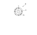
- FIG. 1G shows a cross section perpendicular to the longitudinal direction of the conductive material 18 with a sealing function according to the second embodiment of the present invention.
- the conducting material 18 with a sealing function is formed by inserting a linear solid conducting material 11 into a hollow tube 12 c of a tubular (tubular) sealing material 12.
- the solid conducting material 11 and the sealing material 12 may be in partial contact.
- the first electrode provided on the first base material and the second electrode provided on the second base material include the above-described conductive material with a sealing function. Are arranged opposite to each other.
- an electric module a dye-sensitized solar cell is illustrated as an example, and the electric module of this embodiment will be described.
- the present invention is not limited to a dye-sensitized solar cell, and is sealed between cells. And can be applied to electrical modules that require serial connection or parallel connection.
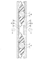
- FIG. 2 is a schematic cross-sectional view showing the dye-sensitized solar cell of the present embodiment.
- the dye-sensitized solar cell 20 of the present embodiment is generally configured by a semiconductor electrode 21, a counter electrode 22, an electrolyte 23, and a conductive material 10 with a sealing function.
- the semiconductor electrode 21 includes a base material 25, a transparent conductive film 26 stacked on the base material 25, and a semiconductor layer 27 stacked on the transparent conductive film 26.
- a known sensitizing dye is adsorbed on the surface of the semiconductor layer 27 in contact with the electrolyte 23 including the porous interior.
- the counter electrode 22 includes a base material 29, a counter conductive film 30 stacked on the base material 29, and a catalyst layer 31 stacked on the counter conductive film 30.
- the encapsulant 12 of the conducting material 10 with the encapsulating function is provided to form a solar cell power generation unit including the semiconductor electrode 21, the counter electrode 22, and the electrolyte 23 on the outer periphery of the semiconductor layer 27. . That is, the conductive material with a sealing function 10 forms a gap between the semiconductor electrode 21 and the counter electrode 22, and the electrolyte 23 is sealed in the gap.
- the solid conducting material 11 of the conducting material 10 with the sealing function is in direct contact with the transparent conductive films 26 and 30 provided on the base materials 25 and 29 of the semiconductor electrode 21 and the counter electrode 22, and the sealing material 12 is It is provided so as to be in close contact with the solid conductive material 11 without any gap and in close contact with the transparent conductive films 26 and 30 of the semiconductor electrode 21 and the counter electrode 22.
- the sealing material 12 seals the electrolyte 23 in the gap between the semiconductor electrode 21 and the counter electrode 22. Further, the solid conductive material 11 is in direct contact with the transparent conductive films 26 and 30 of the semiconductor electrode 21 and the counter electrode 22 on the side opposite to the side where the sealing material 12 is in contact with the electrolyte 23.
- first solar cell / (sealing material 12 / solid conducting material 11 / sealing material 12) / (second solar cell) Cell) / (sealing material 12 / solid conducting material 11 / sealing material 12).
- the material of the base materials 25 and 29 constituting the semiconductor electrode 21 and the counter electrode 22 is not particularly limited, and may be any of glass, resin, and metal.
- a transparent conductive film or a counter conductive film may be formed on the adhesion surface of the substrate to which the curable resin composition adheres.
- the resin (plastic) those having visible light permeability are preferable, and examples thereof include poly (meth) acrylic acid ester, polycarbonate, polyester, polyimide, polystyrene, polyvinyl chloride, and polyamide.
- the substrates 25 and 29 are preferably plastic transparent substrates, and more preferably PET films or PEN films.
- the kind of the transparent conductive film 26 and the counter conductive film 30 is not particularly limited, and a conductive film used for a conventionally known dye-sensitized solar cell can be applied.
- a thin film made of a metal oxide can be given. It is done.
- Metal oxides include indium oxide / tin oxide (ITO), fluorine-doped tin oxide (FTO), zinc oxide, tin oxide, antimony-doped tin oxide (ATO), indium oxide / zinc oxide (IZO), gallium oxide / oxide Zinc (GZO), titanium oxide, etc. are mentioned.
- ITO indium oxide / tin oxide
- FTO fluorine-doped tin oxide
- ATO antimony-doped tin oxide
- IZO indium oxide / zinc oxide
- GZO gallium oxide / oxide Zinc
- titanium oxide etc.
- the semiconductor layer 27 has a function of receiving and transporting electrons from a sensitizing dye described later, and is formed on the surface 26 a of the transparent conductive film 26 by a semiconductor made of a metal oxide.
- the metal oxide include titanium oxide (TiO 2 ), zinc oxide (ZnO), and tin oxide (SnO 2 ).
- Examples of the sensitizing dye supported on the semiconductor layer 27 include organic dyes and metal complex dyes.
- Examples of organic dyes include coumarin, polyene, cyanine, hemicyanine, and thiophene.
- As the metal complex dye for example, a ruthenium complex is preferably used.
- the material constituting the catalyst layer 31 conventionally known materials can be applied, and examples thereof include carbons such as platinum and carbon nanotubes, and conductive polymers (for example, PEDOT / PSS).
- an electrolytic solution used in a conventionally known dye-sensitized solar cell can be applied.
- an electrolytic solution for a dye-sensitized solar cell a solution obtained by dissolving a redox couple (electrolyte) in a solvent is generally used.
- An organic solvent can be used as a component of the electrolyte 23. Examples of the organic solvent include alcohols, nitriles, ethers, esters, ketones, hydrocarbons, halogenated hydrocarbons, and the like.
- a conventionally known redox couple can be applied.
- the redox pair include a combination of iodine molecules such as sodium iodide and iodide, or a combination of bromine molecules such as potassium bromide and bromide.
- the semiconductor electrode 21 and the counter electrode 22 are bonded using the conductive material 10 with a sealing function in which the solid conductive material 11 and the sealing material 12 are integrated. Therefore, the solid conductive material 11 for electrically connecting the semiconductor electrode 21 and the counter electrode 22 and the sealing material 12 for bonding the semiconductor electrode 21 and the counter electrode 22 are accurately arranged at predetermined positions. . Therefore, when it is necessary to increase the aperture ratio of the solar battery cell, even if the line widths of the solid conductive material 11 and the sealing material 12 are reduced, the solid conductive material 11 and the sealing material 12 may be misaligned. Absent.
- the semiconductor electrode 21 and the counter electrode 22 are formed using the conductive material 10 with a sealing function in which the solid conductive material 11 and the sealing material 12 are integrated in advance. Since it adheres, the malfunction that a space
- the manufacturing method of the electric module of this embodiment manufactures the electric module provided with the 1st electrode provided on the 1st base material, and the 2nd electrode provided on the 2nd base material.
- the method includes a step A in which the first electrode and the second electrode are opposed to each other through the conductive material with a sealing function of the above-described embodiment, and a solid conductive material of the conductive material with a sealing function.
- the first electrode and the second electrode are brought into direct contact with each other, and the sealing material of the conductive material with a sealing function is brought into close contact with the solid conductive material without gaps, and is brought into close contact with the first electrode and the second electrode.
- Step B Each of the above steps is performed in the order described.
- a dye-sensitized solar cell is illustrated as an example of the electric module, and the method for manufacturing the electric module of the present embodiment will be described with reference to FIGS. 2 and 3.
- a transparent conductive film 26 made of ITO or the like is formed on one surface of the substrate 25 by a known method such as a sputtering method, a printing method, or a spray method.
- a semiconductor layer 27 is formed on the transparent conductive film 26 formed on one surface of the substrate 25.
- a method for forming the semiconductor layer 27 is not particularly limited.
- a method of applying a paste containing metal oxide particles on the transparent conductive film 26 by a printing method, a method of spraying metal oxide particles, or the like. can be mentioned.
- a semiconductor electrode including a base material 25, a transparent conductive film 26 formed on one surface of the base material 25, and a semiconductor layer 27 stacked on the transparent conductive film 26. 21 is obtained.
- spraying method As a method for spraying metal oxide particles such as titanium oxide (hereinafter abbreviated as “spraying method”), a known method is used. For example, a thermal spraying method, a cold spray method, an aerosol deposition method (hereinafter referred to as “the spraying method”). Abbreviated as “AD method”).
- the method (step) for adsorbing the sensitizing dye to the obtained semiconductor layer 27 is not particularly limited.
- the semiconductor layer 27 is immersed in a sensitizing dye solution in which the sensitizing dye is dissolved in a solvent, and the semiconductor layer 27 is immersed in the semiconductor layer 27.
- Examples thereof include a method of supporting a sensitizing dye.
- a roll-to-roll method in which the semiconductor layer 27 formed on a long film base material is continuously put into a sensitizing dye solution, immersed, and then pulled up can be employed.
- the counter conductive film 30 made of ITO, zinc oxide, platinum, or the like is formed on one surface of the base material 29 by a sputtering method, a printing method, a spray method, or the like. Further, a method of forming the catalyst layer 31 by applying a carbon paste or the like on the surface of the counter conductive film 30 can be mentioned. With this method, as shown in FIG. 3, a counter electrode comprising a base material 29, a counter conductive film 30 formed on one surface of the base material 29, and a catalyst layer 31 laminated on the counter conductive film 30. 22 is obtained.
- the conductive material 10 with a sealing function is arranged with a predetermined width dimension on the outer peripheral portion (boundary of each solar battery cell) of the surface facing the counter electrode 22 in the semiconductor electrode 21.
- the conductive material with a sealing function 10 may be arranged on the outer peripheral portion so as to surround the semiconductor layer 26 in a frame shape having a predetermined width dimension.
- the sealing material 12 constituting the conductive material with a sealing function 10 disposed on the electrode is a curable resin, it is disposed in an uncured or semi-cured state, and the sealing material 12 is a thermoplastic resin. Are arranged in a non-molten state (solid state).
- Step A the semiconductor electrode 21 and the counter electrode 22 are arranged to face each other through the conductive material 10 with a sealing function.
- Step B the sealing material 12 which comprises the conduction
- Step B when a hot melt adhesive (thermoplastic resin) is used as the sealing material 12, the sealing is performed at a temperature not lower than the temperature at which the hot melt adhesive melts and not higher than the temperature at which the substrates 25 and 29 are not melted.
- the material 12 is heated. Along with this heating, the semiconductor electrode 21 and the counter electrode 22 are pressed inward in the thickness direction (the direction of the arrow ⁇ shown in FIG. 3).
- the molten hot melt adhesive (sealing material 12) flows in a direction perpendicular to the thickness direction of the semiconductor electrode 21 and the counter electrode 22 (in the direction of the arrow ⁇ shown in FIG. 3), and faces the semiconductor electrode 21 and the counter electrode.
- the solid conductive material 11 is exposed at the portion in contact with the electrode 22.
- the exposed solid conductive material 11 is in direct contact with the semiconductor electrode 21 and the counter electrode 22, and the sealing material 12 is in close contact with the semiconductor electrode 21 and the counter electrode 22 at the outer peripheral portion of the semiconductor layer 27.
- the sealing material 12 flows so as to slide on the surface of the solid conductive material 11 while being in contact with the solid conductive material 11 without being separated (separated) from the solid conductive material 11.
- the material 12 is kept in close contact with no gap.
- the sealing material 12 When a hot melt adhesive is used as the sealing material 12, the solid conductive material 11 is in direct contact with the transparent conductive films 26 and 30 of the semiconductor electrode 21 and the counter electrode 22, and the sealing material 12 is in contact with the solid conductive material 11. After being provided in close contact with the gap and in close contact with the semiconductor electrode 21 and the counter electrode 22, by stopping the heating of the sealing material 12 and stopping applying pressure to the semiconductor electrode 21 and the counter electrode 22, Adhesion between the semiconductor electrode 21 and the counter electrode 22 is completed.
- the sealing material 12 when a thermosetting resin or an ultraviolet curable resin is used as the sealing material 12, the semiconductor electrode 21 and the counter electrode 22 are pressed inward in the thickness direction (the direction of the arrow ⁇ shown in FIG. 3). To do.
- the uncured sealing material 12 flows in a direction perpendicular to the thickness direction of the semiconductor electrode 21 and the counter electrode 22 (in the direction of the arrow ⁇ shown in FIG. 3) and comes into contact with the semiconductor electrode 21 and the counter electrode 22. In the portion, the solid conductive material 11 is exposed. Further, the exposed solid conductive material 11 is in direct contact with the semiconductor electrode 21 and the counter electrode 22, and the sealing material 12 is in close contact with the semiconductor electrode 21 and the counter electrode 22 at the outer peripheral portion of the semiconductor layer 27.
- the sealing material 12 flows so as to slide on the surface of the solid conductive material 11 while being in contact with the solid conductive material 11 without being separated (separated) from the solid conductive material 11. The material 12 is kept in close contact with no gap.
- the sealing material 12 When a thermosetting resin or an ultraviolet curable resin is used as the sealing material 12, the solid conductive material 11 directly contacts the transparent conductive films 26 and 30 of the semiconductor electrode 21 and the counter electrode 22, and the sealing material 12 After being provided in close contact with the solid conducting material 11 without gaps and in close contact with the semiconductor electrode 21 and the counter electrode 22, by heating the sealing material 12 or irradiating the sealing material 12 with ultraviolet rays, The sealing material 12 is cured to complete the bonding between the semiconductor electrode 21 and the counter electrode 22.
- a thermosetting resin or an ultraviolet curable resin is used as the sealing material 12 12
- the sealing material 12 After being provided in close contact with the solid conducting material 11 without gaps and in close contact with the semiconductor electrode 21 and the counter electrode 22, by heating the sealing material 12 or irradiating the sealing material 12 with ultraviolet rays, The sealing material 12 is cured to complete the bonding between the semiconductor electrode 21 and the counter electrode 22.
- the process A and the process B can be similarly performed when the conductive materials 13 to 18 with the sealing function are used.
- the transparent conductive films of the semiconductor electrode 21 and the counter electrode 22 from above and below the conductive material 13 with a sealing function, respectively, as shown in FIG.
- the sealing material 12 covering the solid conductive material 11 flows in the ⁇ direction, and the solid conductive material 11 and the transparent conductive films 26 and 30 are in direct contact with each other so that both electrodes are in contact with each other. Electrically connected.
- the sealing material 12 flowing in the ⁇ direction bonds the semiconductor electrode 21 and the counter electrode 22 and seals a predetermined portion of each solar battery cell.
- the conductive cells 13 to 18 with the sealing function are sandwiched between the semiconductor electrode 21 and the counter electrode 22 so as to be sealed, thereby sealing the solar battery cell and electrically connecting both electrodes. it can.
- both electrodes can be crimped
- both electrodes can be obtained by heating or irradiating the sealing material 12 after pressing or during pressing. Can be crimped.
- the conductive material 10 with the sealing function is placed between the semiconductor electrode 21 and the counter electrode 22 in Step A. It is preferable to arrange in.
- the conductive material 10 with a sealing function is divided into two along its central axis. Then, the solid conductive material 11 is exposed to the central portion of the solid conductive material 11 while the outer peripheral surface of the solid conductive material 11 is covered with the sealing material 12, and the solid conductive material is formed of a conductive foil provided with the sealing material 12 on both surfaces.
- Examples include a method of cutting the material 11 along the both surfaces (in a strip shape) and exposing the solid conductive material 11 to the cut surface.
- a joined body formed by bonding the semiconductor electrode 21 and the counter electrode 22 is placed in a reduced-pressure atmosphere, the liquid injection hole is immersed in a container (not shown) holding the electrolytic solution, and the electrolytic solution is removed by evacuation. Inject into the internal space. After injecting the electrolytic solution, the injection hole is sealed with an adhesive or the like, and the internal space is sealed.
- the semiconductor electrode 21 and the counter electrode 22 are arranged to be opposed to each other with a predetermined gap and bonded via the sealing material 12, and an electrolytic solution as the electrolyte 23 is interposed between the electrodes.
- the dye-sensitized solar cell 20 filled with is obtained.
- the conductive material with a sealing function can be prepared in advance in a separate process from the electrical module manufacturing method of the present embodiment.
- a conductive material with a sealing function may be produced with the progress of the above-described Step A and Step B, and the conductive material with a sealing function may be supplied to Step A described above.
- a line for producing a conductive material with a sealing function is provided along the production line for performing the processes A and B, and the line for producing the conductive material with a sealing function is directly sealed from the line for producing the conductive material with a sealing function to the line for performing the process A.
- a conductive material with a stopping function can be supplied.
- the semiconductor electrode 21 and the counter electrode 22 are bonded using the conductive material 10 with a sealing function in which the solid conductive material 11 and the sealing material 12 are integrated. Therefore, the solid conductive material 11 for electrically connecting the semiconductor electrode 21 and the counter electrode 22 and the sealing material 12 for bonding the semiconductor electrode 21 and the counter electrode 22 are collectively disposed at a predetermined position. can do. Therefore, it is not necessary to arrange the solid conductive material 11 and the sealing material 12 separately, and the process can be simplified.
- the semiconductor electrode 21 and the counter electrode 22 are used using the conductive material 10 with a sealing function in which the solid conductive material 11 and the sealing material 12 are integrated.
- the solid conductive material 11 and the sealing material 12 can be reduced even if the line width of the solid conductive material 11 and the sealing material 12 is reduced. There is no need to align the sealing material 12 separately, and the solid conducting material 11 and the sealing material 12 can be easily aligned.
- the semiconductor electrode 21 and the counter electrode 22 are used using the conductive material 10 with a sealing function in which the solid conductive material 11 and the sealing material 12 are integrated. Therefore, when the conductive material 10 with a sealing function is disposed, the adhesion between the solid conductive material 11 and the sealing material 12 is reduced, and a gap is generated between the solid conductive material 11 and the sealing material 12. Can be prevented.
- Example 1 "Production of dye-sensitized solar cells"
- a hot melt adhesive (trade name: High Milan 1652, manufactured by Mitsui DuPont Polychemical Co., Ltd.) was placed in a metal container and heated to 120 ° C. to be melted.
- a copper wire having a circular cross section and a diameter of 100 ⁇ m was used as the solid conductive material. The copper wire was brought into contact with the molten hot melt adhesive, and then pulled up from the hot melt adhesive to solidify the hot melt adhesive on the surface of the copper wire.
- the diameter of the obtained conductive material with a sealing function was 1 mm.
- the obtained conducting material with a sealing function is inserted into an elliptical hole having a minor axis diameter of 100 ⁇ m and a major axis diameter of 1 mm, and a part of the hot melt adhesive covering the copper wire is scraped off.
- a conductive material with a sealing function having a cross section shown was obtained. This was cut to a length of 1 m, and five conductive materials with a sealing function having the same length were produced.
- titanium oxide particles having an average particle diameter of 100 nm were sprayed by the AD method.
- six rows of porous titanium oxide layers having a length of 1 m and a width of 1 cm were formed. At this time, the interval between the rows was set to 2 mm.
- titanium oxide was formed on the ITO film forming surface at a position 0.5 mm from the right end of each row of the titanium oxide porous layer.
- Laser light was irradiated in parallel with the longitudinal direction of the porous layer, a part of the ITO film was removed, and a part of the PET substrate was exposed.
- a porous titanium oxide is formed in a region corresponding to a power generation region of six solar cells connected in series later. Layers were placed. At this time, an area where the ITO film was exposed was left in the vicinity of the titanium oxide porous layer of each solar battery cell, where the conductive material with a sealing function was placed later.
- a dye solution was prepared by dissolving a metal complex dye (Solaronics Luthenizer 535) in acetonitrile at a concentration of 0.1 g / L. Using a coating apparatus (manufactured by Unitech Co., Ltd.), after impregnating the dye solution from above the titanium oxide porous layer, acetonitrile was dried and removed to adsorb the metal complex dye on titanium oxide.
- a metal complex dye Smallonics Luthenizer 535
- acetonitrile was dried and removed to adsorb the metal complex dye on titanium oxide.
- the conductive material with a sealing function was disposed so as to surround each titanium oxide porous layer.
- 30 ⁇ L of an iodine-based electrolyte (trade name: Iodolite Z-50) manufactured by Solaronics was dropped on the porous titanium oxide layer surrounded by the conductive material with a sealing function.
- the solvent was volatilized to form a conductive catalyst layer containing carbon at a predetermined location on the ITO film.
- laser light was irradiated in parallel with the longitudinal direction of the catalyst layer to remove part of the catalyst layer and the ITO film, thereby exposing part of the PET substrate.
- the PET base material on which the catalyst layer was formed was placed on the PET base material provided with the titanium oxide porous layer onto which the iodine electrolyte solution was dropped. At this time, the PET base materials were arranged so that the titanium oxide porous layer and the catalyst layer face each other with the conductive material with a sealing function interposed therebetween. Further, the PET base material on which the catalyst layer was formed was placed so that each of the six exposed straight portions of PET was positioned at a position of 0.5 mm from the left end of each row of the six titanium oxide porous layers. . Next, the two PET base materials superimposed are heated to 120 ° C. and pressed in the thickness direction of the two PET base materials, and the conduction with a sealing function sandwiched between the two PET base materials.
- the number of contact failures occurring in the ITO film provided with the titanium oxide porous layer is shown in the column “Location where the sealing material flows between the solid conductive material and ITO” in Table 1.
- the number of contact failures occurring in the catalyst layer is shown in the column of “Location where the sealing material flows between the solid conductive material and the catalyst layer” in Table 1.
- Thermosetting resin composition as a sealing material (trade name: Epicron 850, manufactured by DIC, phenolic curing agent, trade name: MEH7851-H, Meiwa Kasei Co., Ltd., curing accelerator, trade name: 2E4MZ- CN, manufactured by Shikoku Kasei Co., Ltd.) was dissolved to prepare a methyl ethyl ketone solution containing a thermosetting resin. At that time, the total concentration was adjusted to 50 g / L, and the molar ratio of epoxy group: phenolic hydroxyl group: imidazole ring was adjusted to 100: 90: 1.
- the cross-sectional shape is circular and the diameter of the copper wire is 100 ⁇ m.
- the copper wire is brought into contact with the methyl ethyl ketone solution, it is pulled up from the methyl ethyl ketone solution and dried in the air. Methyl ethyl ketone was volatilized.
- a conductive material with a sealing function was obtained in which the surface of the copper wire was coated with an adhesive made of a thermosetting resin composition having a thickness of 450 ⁇ m.
- the diameter of the obtained conductive material with a sealing function was 1 mm.
- the obtained conductive material with a sealing function is inserted into an elliptical hole having a minor axis diameter of 100 ⁇ m and a major axis diameter of 1 mm, and a part of the adhesive made of a thermosetting resin composition covering a copper wire is used. I scraped off. Next, the conductive material with a sealing function was cut to have a length of 1 m, and five conductive materials with a sealing function having the same length were produced.
- Example 2 In the same manner as in Example 1, the first PET substrate on which the titanium oxide porous layer was formed and the second PET substrate on which the catalyst layer was formed were used to face both substrates.
- the conductive material with a sealing function was sandwiched between both base materials.
- the adhesive composed of the thermosetting resin composition constituting the conductive material with a sealing function is cured by heating two PET substrates in the thickness direction while heating at 160 ° C. for 1 hour.
- the two PET substrates were bonded and sealed.
- the ITO film left exposed in the vicinity of the titanium oxide porous layer, and the catalyst layer in a portion facing the ITO film are formed by the copper wire constituting the conductive material with a sealing function. Electrically connected.
- a dye-sensitized solar cell of Example 2 in which six solar cells were connected in series through a predetermined path was obtained.
- Example 2 About the dye-sensitized solar cell obtained in Example 2, it carried out similarly to Example 1, and evaluated the state of sealing and an electrical connection. The results are shown in Table 1.
- Example 3 A dye-sensitized solar cell of Example 3 was obtained in the same manner as Example 1 except that a copper ribbon having a width and thickness of 100 ⁇ m was used instead of the copper wire as the solid conductive material. About the obtained dye-sensitized solar cell, it carried out similarly to Example 1, and evaluated the state of sealing and electrical connection. The results are shown in Table 1.
- a hot melt adhesive (trade name: Himiran 1652, manufactured by Mitsui DuPont Polychemical Co., Ltd.) was molded into a ribbon having a width of 450 ⁇ m and a thickness of 100 ⁇ m, and further cut into a string having a length of 1 m.
- the first PET substrate on which the titanium oxide porous layer was formed and the second PET substrate on which the catalyst layer was formed were used to face both substrates.
- the sealing material and a solid conductive material made of a circular copper wire having a cross-sectional diameter of 100 ⁇ m are arranged in order between the two base materials in order, and the sealing material and the solid conductive material was sandwiched between both PET substrates. Subsequently, the two PET base materials are heated to 120 ° C., and the two PET base materials are pressed in the thickness direction to form a sealing material sandwiched between the two PET base materials. Two PET substrates were bonded and sealed with a hot melt adhesive. About the dye-sensitized solar cell of the comparative example 1 obtained by this method, it carried out similarly to Example 1, and evaluated the state of sealing and electrical connection. The results are shown in Table 1. Among the observed voids, there was a void having a diameter exceeding 0.3 mm when the void was approximated to a circle in plan view. Such a large gap was not observed in the case of the example.
- thermosetting resin composition in a semi-cured state formed on the plate surface was cut into a sheet having a thickness of 100 ⁇ m.
- a sealing material made of a ribbon-like thermosetting resin composition having a width of 450 ⁇ m, a thickness of 100 ⁇ m, and a length of 1 m was obtained.
- the first PET substrate on which the titanium oxide porous layer was formed and the second PET substrate on which the catalyst layer was formed were used to face both substrates.
- the sealing material and a solid conductive material made of a circular copper wire having a cross-sectional diameter of 100 ⁇ m are arranged in order between the two base materials in order, and the sealing material and the solid conductive material was sandwiched between both PET substrates. Subsequently, the two PET base materials were pressed in their thickness direction, and the two PET base materials were heated at 160 ° C. for 1 hour to be sandwiched between the two PET base materials. Two PET base materials were bonded and sealed with a thermosetting resin composition as a sealing material. About the dye-sensitized solar cell of the comparative example 2 obtained by this method, it carried out similarly to Example 1, and evaluated the state of sealing and electrical connection. The results are shown in Table 1. Among the observed voids, there was a void having a diameter exceeding 0.3 mm when the void was approximated to a circle in plan view. Such a large gap was not observed in the case of the example.
- Examples 1 to 3 compared to Comparative Examples 1 and 2, the solid conducting material and the sealing material could be easily and accurately arranged at almost predetermined positions.
- the reason why the excellent results of Examples 1 to 3 were obtained is that the solid conductive material and the sealing material constituting the conductive material with the sealing function are integrated, so that both of these members are used in the sealing process. It was possible to install together.
- the solid conductive material and the sealing material are sufficiently adhered, and the sealing material and each electrode are sufficiently adhered, There were very few voids formed between them.
- Example 1 to 3 as compared with Comparative Examples 1 and 2, the sealing was performed between the solid conducting material and the ITO film provided with the titanium oxide porous layer, and between the solid conducting material and the catalyst layer. There were few places where stopping material flowed. That is, an electrical connection between the solid conductive material and the conductive portion (ITO film and catalyst layer) of each PET substrate was formed, and contact failure between them could be suppressed.
- Example 4 In Example 1, a part of the hot melt adhesive covering the copper wire was scraped off by inserting the conductive material with a sealing function covered with the hot melt adhesive into the elliptical hole. In this example, the above-described shaving off is not performed, and a dye-sensitized solar cell as in Example 1 is used except that a conductive material with a sealing function in which a copper wire is not exposed as shown in FIG. 1B is used. Was made. As a result, the hot melt adhesive constituting the conductive material with a sealing function heated in a state of being pressed by the two PET base materials flowed in the ⁇ direction as shown in FIG.
- the two PET substrates could be electrically connected by directly contacting each conductive part (ITO film and catalyst layer) of the PET substrate.
- ITO film and catalyst layer conductive part of the PET substrate.
- Example 5 an adhesive covering a copper wire by inserting a conductive material with a sealing function covered with an adhesive (sealing material) made of a thermosetting resin composition through an elliptical hole. Part of the agent was scraped off. In this example, the above-described shaving off is not performed, and a dye-sensitized solar cell as in Example 2 is used except that a conductive material with a sealing function in which a copper wire is not exposed as shown in FIG. 1B is used. Was made. As a result, as a result of the adhesive comprising the thermosetting resin composition constituting the conductive material with a sealing function pressed by the two PET base materials flowing in the ⁇ direction as shown in FIG.
- the two PET base materials could be electrically connected by directly contacting each conductive part (ITO and catalyst layer) of the two PET base materials. Then, each solar cell was able to be sealed by making it thermoset by heating. About the dye-sensitized solar cell produced by the present Example, it carried out similarly to Example 1, and evaluated the state of sealing and electrical connection. The result was excellent as in Example 2.
- Example 6 A conducting material with a sealing function having a cross-sectional shape as shown in FIG. 1G, in which a copper wire having a diameter of about 100 ⁇ m is inserted into a hollow resin tube (inner diameter of more than 100 ⁇ m, outer diameter of about 1 mm) made of thermoplastic resin.
- a dye-sensitized solar cell was produced in the same manner as in Example 1 except that this conductive material with a sealing function was used.
- the hot melt adhesive constituting the conductive material with a sealing function heated in a state of being pressed by the two PET base materials flowed in the ⁇ direction as shown in FIG.
- each solar cell was able to be sealed.
- the dye-sensitized solar cell produced by the present Example it carried out similarly to Example 1, and evaluated the state of sealing and electrical connection. As a result, the number of voids between the encapsulant and the copper wire was larger than in Example 1, but the other evaluations were excellent as in Example 1.
- the first base material on which the titanium oxide porous layer was formed and the second base material on which the catalyst layer was formed Adhering with a sealing material, forming an electrical connection between both base materials with a solid conductive material, allowing a plurality of solar cells to be connected in series or in parallel, and electrolysis within each solar cell with a sealing material It was confirmed that the liquid could be reliably sealed.
- the present invention is widely applicable in the field relating to electrical modules such as dye-sensitized solar cells.
- Conductive Material with Sealing Function 11 Solid Conductive Material 12 Sealing Materials 13-18 Conductive Material with Sealing Function 20 Dye-sensitized Solar Cell 21 Semiconductor Electrode 22 Counter Electrode 23 Electrolyte 25 Base Material 26 Transparent Conductive Film 27 Semiconductor Layer 29 Base Material 30 Opposing conductive film 31 Catalyst layer
Landscapes
- Chemical & Material Sciences (AREA)
- Chemical Kinetics & Catalysis (AREA)
- Electrochemistry (AREA)
- Engineering & Computer Science (AREA)
- Power Engineering (AREA)
- Microelectronics & Electronic Packaging (AREA)
- Hybrid Cells (AREA)
- Photovoltaic Devices (AREA)
Abstract
固形導通材(11)が封止材(12)によって直接保持されてなる封止機能付導通材(10)。
Description
本発明は、封止機能付導通材、電気モジュール、電気モジュールの製造方法に関する。本願は、2013年12月3日に日本に出願された特願2013-250422号に基づき優先権を主張し、その内容をここに援用する。
従来、封止を必要とする電気モジュールにおいては、複数のセルを同一平面内に並べて作製する際に、例えば、隣接するセル間において、第一のセル1の上側電極と、第二のセル2の下側電極とを電気的に接続し、かつ電極間に電解質等の要素を封止するために、「封止材/導通材(例えば導線、導電ペースト等)/封止材」の構造を形成している。
前記構造の電気モジュールとしては、例えば、透明電極と対向電極を備えた色素増感太陽電池素子が、同一平面内に並んで設けられた色素増感太陽電池モジュールが挙げられる。隣り合う素子同士を電気的に接続するために、第一の素子の対向電極が素子間のギャップにも存在して、第二の素子の透明電極と直接接続した電気モジュールが開示されている(特許文献1参照)。
透明電極と、対向電極と、これらを封止して絶縁する封止絶縁部と、を備えた光電変換素子が同一平面内に並んで設けられた光電変換モジュールにおいて、隣り合う光電変換素子同士を電気的に接続するために、第一の光電変換素子の透明電極部材の一部と、第二の光電変換素子の対向電極部材の一部を、互いに向き合わせ、その間に導通材を設けることにより、複数のセル間での直列構造を形成した光電変換モジュールが開示されている(特許文献2参照)。
しかし、従来の電気モジュールでは、封止材/導通材/封止材の構造において、これらの部材を同一方向(例えば、下側電極の表面に沿う方向)に位置合わせして並べるのが難しく、非常に手間がかかるという課題があった。例えば、セルの開口率(=非封止材面積/基板面積)を大きくする目的で、封止材と導通材の線幅を小さくすると、封止材と導通材の位置合わせが非常に難しくなるという課題があった。さらに、封止材と導通材を別々に配設すると、封止材と導通材とが十分に密着しないため、封止材と導通材の間に空隙が生じやすくなるという課題があった。
本発明は、上記事情に鑑みてなされたものであって、対向する一対の電極を電気的に接続するための導通材と、それらの電極を接着し、封止する封止材とを一括して配設することが可能な封止機能付導通材、それを用いた電気モジュール、および電気モジュールの製造方法の提供を目的とする。
[1]固形導通材が封止材によって直接保持されてなる封止機能付導通材。
[2]固形導通材と封止材が一体化されてなる前記[1]に記載の封止機能付導通材。
[3]前記固形導通材は、導線、導電チューブおよび導電メッシュから選ばれる1種である前記[2]に記載の封止機能付導通材。
[4]前記封止材は、長手方向と垂直な断面の形状が略円形状(リール状)または略角形状(リボン状)である前記[2]または[3]に記載の封止機能付導通材。
[5]前記固形導通材の一部が長手方向に沿って露出している前記[2]~[4]のいずれか1項に記載の封止機能付導通材。
[6]線状の固形導通材が管状の封止材に挿通されてなる前記[1]に記載の封止機能付導通材。
[7]第1の基材上に設けられた第1の電極と、第2の基材上に設けられた第2の電極とが、前記[1]~[6]のいずれか1項に記載の封止機能付導通材を介して対向配置されてなる電気モジュール。
[8]前記封止機能付導通材は、前記固形導通材が、前記第1の電極および前記第2の電極に直接接触し、かつ、前記封止材が、前記固形導通材と隙間なく密着するとともに、前記第1の電極および前記第2の電極に密着するように設けられた前記[7]に記載の電気モジュール。
[9]第1の基材上に設けられた第1の電極と、第2の基材上に設けられた第2の電極と、を備えた電気モジュールの製造方法であって、前記[1]~[6]のいずれか1項に記載の封止機能付導通材を介して、前記第1の電極と前記第2の電極とを対向配置する工程Aと、前記固形導通材を、前記第1の電極および前記第2の電極に直接接触させ、かつ、前記封止材を、前記固形導通材と隙間なく密着させるとともに、前記第1の電極および前記第2の電極に密着させる工程Bと、を有する電気モジュールの製造方法。
[10]前記封止材を分割し、予め前記固形導通材を露出させた後、前記封止機能付導通材を、前記第1の電極と前記第2の電極の間に配置する前記[9]に記載の電気モジュールの製造方法。
[11]予め別工程で作製した前記封止機能付導通材を用いる前記[9]または[10]に記載の電気モジュールの製造方法。
[12]前記工程Aと前記工程Bの進行に伴って、前記封止機能付導通材を作製し、前記工程Aに前記封止機能付導通材を供給する前記[9]または[10]に記載の電気モジュールの製造方法。
[2]固形導通材と封止材が一体化されてなる前記[1]に記載の封止機能付導通材。
[3]前記固形導通材は、導線、導電チューブおよび導電メッシュから選ばれる1種である前記[2]に記載の封止機能付導通材。
[4]前記封止材は、長手方向と垂直な断面の形状が略円形状(リール状)または略角形状(リボン状)である前記[2]または[3]に記載の封止機能付導通材。
[5]前記固形導通材の一部が長手方向に沿って露出している前記[2]~[4]のいずれか1項に記載の封止機能付導通材。
[6]線状の固形導通材が管状の封止材に挿通されてなる前記[1]に記載の封止機能付導通材。
[7]第1の基材上に設けられた第1の電極と、第2の基材上に設けられた第2の電極とが、前記[1]~[6]のいずれか1項に記載の封止機能付導通材を介して対向配置されてなる電気モジュール。
[8]前記封止機能付導通材は、前記固形導通材が、前記第1の電極および前記第2の電極に直接接触し、かつ、前記封止材が、前記固形導通材と隙間なく密着するとともに、前記第1の電極および前記第2の電極に密着するように設けられた前記[7]に記載の電気モジュール。
[9]第1の基材上に設けられた第1の電極と、第2の基材上に設けられた第2の電極と、を備えた電気モジュールの製造方法であって、前記[1]~[6]のいずれか1項に記載の封止機能付導通材を介して、前記第1の電極と前記第2の電極とを対向配置する工程Aと、前記固形導通材を、前記第1の電極および前記第2の電極に直接接触させ、かつ、前記封止材を、前記固形導通材と隙間なく密着させるとともに、前記第1の電極および前記第2の電極に密着させる工程Bと、を有する電気モジュールの製造方法。
[10]前記封止材を分割し、予め前記固形導通材を露出させた後、前記封止機能付導通材を、前記第1の電極と前記第2の電極の間に配置する前記[9]に記載の電気モジュールの製造方法。
[11]予め別工程で作製した前記封止機能付導通材を用いる前記[9]または[10]に記載の電気モジュールの製造方法。
[12]前記工程Aと前記工程Bの進行に伴って、前記封止機能付導通材を作製し、前記工程Aに前記封止機能付導通材を供給する前記[9]または[10]に記載の電気モジュールの製造方法。
[13]第1の基材上に設けられた複数の第1電極と、第2の基材上に設けられた複数の第2電極とが対向配列されてなる電気モジュールであって、前記[1]~[4]のいずれか1項に記載の封止機能付導通材により、複数のセルに分割され、かつ、互いに隣接するセルの第1電極と第2電極とが導通されてなる電気モジュールが、好ましい実施形態の一例として挙げられる(図2,3参照)。
[14]第1の基材上に設けられた複数の第1電極と、第2の基材上に設けられた複数の第2電極と、を備えた電気モジュールの製造方法であって、前記[1]~[4]のいずれか1項に記載の封止機能付導通材を介して、前記複数の第1電極と前記複数の第2電極とを複数のセルが形成されるように対向配置する工程Aと、前記固形導通材を、互いに隣接するセルのうち一方のセルの前記第1電極と他方のセルの前記第2電極に直接接触させ、かつ、前記封止材を、前記固形導通材と密着させるとともに、前記第1電極および前記第2電極に密着させる工程Bと、を有する電気モジュールの製造方法が、好ましい実施形態の一例として挙げられる(図2,3参照)。
[14]第1の基材上に設けられた複数の第1電極と、第2の基材上に設けられた複数の第2電極と、を備えた電気モジュールの製造方法であって、前記[1]~[4]のいずれか1項に記載の封止機能付導通材を介して、前記複数の第1電極と前記複数の第2電極とを複数のセルが形成されるように対向配置する工程Aと、前記固形導通材を、互いに隣接するセルのうち一方のセルの前記第1電極と他方のセルの前記第2電極に直接接触させ、かつ、前記封止材を、前記固形導通材と密着させるとともに、前記第1電極および前記第2電極に密着させる工程Bと、を有する電気モジュールの製造方法が、好ましい実施形態の一例として挙げられる(図2,3参照)。
本発明によれば、固形導通材と封止材が一体化されているので、対向する一対の電極を電気的に接続するための導通材と、それらの電極を接着し、封止する封止材とを一括して配設することができる。よって、固形導通材および封止材を所定の位置に容易に配置することができる。さらに、封止後に固形導通材と封止材の間に空隙が生じる割合を低減できる。
本発明の封止機能付導通材、電気モジュール、電気モジュールの製造方法の実施の形態について説明する。なお、本実施の形態は、発明の趣旨を具体的に説明するものであり、本発明を限定するものではない。
<封止機能付導通材>
第一実施形態の封止機能付導通材は、固形導通材と、封止材と、を備え、これらが一体化されてなるものである。
図1Aは、本実施形態の封止機能付導通材の一例を示す概略断面図である。
本実施形態の封止機能付導通材10は、中央に配置された、長手方向と垂直な断面の形状が円形状の固形導通材11と、固形導通材11の外周に、これを被覆するように配置された長手方向と垂直な断面の形状が楕円形状の封止材12と、を備えている。固形導通材11と封止材12の中心は同じ位置にある。図1Aの断面図において、円形の固形導通材11の上端と下端が、楕円形の封止材12の上端と下端に接して、内接している。
第一実施形態の封止機能付導通材は、固形導通材と、封止材と、を備え、これらが一体化されてなるものである。
図1Aは、本実施形態の封止機能付導通材の一例を示す概略断面図である。
本実施形態の封止機能付導通材10は、中央に配置された、長手方向と垂直な断面の形状が円形状の固形導通材11と、固形導通材11の外周に、これを被覆するように配置された長手方向と垂直な断面の形状が楕円形状の封止材12と、を備えている。固形導通材11と封止材12の中心は同じ位置にある。図1Aの断面図において、円形の固形導通材11の上端と下端が、楕円形の封止材12の上端と下端に接して、内接している。
本実施形態の封止機能付導通材10において、固形導通材11と封止材12とが一体化されているとは、固形導通材11と封止材12との間に空隙(ボイド)が存在することなく、両者が互いに密着している状態のことを言う。ここで、封止機能付導通材10の全部で両者が密着していることが好ましいが、一部が密着状態であり、他部が非密着状態であってもよい。
固形導通材11と封止材12との間に空隙が存在する場合は、固形導通材11と封止材12とを分離して得られる封止材12側の分離面において観察される開口(凹部の周縁)を前記空隙の大きさであるとして評価した際に、前記開口を同面積の円と仮定した場合の直径が0.2mm以下であることが好ましく、個数は、100個/mm2以下であることが好ましい。
空隙の前記直径は0.1mm以下がより好ましく、0.05mm以下がさらに好ましい。空隙の個数は、40個/mm2以下がより好ましく、12個/mm2以下がさらに好ましい。
空隙の前記直径が0.15mm以下であり、且つ、空隙の個数が40個/mm2以下であることがより好ましい。
固形導通材11と封止材12との間に空隙が存在する場合は、固形導通材11と封止材12とを分離して得られる封止材12側の分離面において観察される開口(凹部の周縁)を前記空隙の大きさであるとして評価した際に、前記開口を同面積の円と仮定した場合の直径が0.2mm以下であることが好ましく、個数は、100個/mm2以下であることが好ましい。
空隙の前記直径は0.1mm以下がより好ましく、0.05mm以下がさらに好ましい。空隙の個数は、40個/mm2以下がより好ましく、12個/mm2以下がさらに好ましい。
空隙の前記直径が0.15mm以下であり、且つ、空隙の個数が40個/mm2以下であることがより好ましい。
本実施形態の変形例として、例えば図1Bに封止機能付導通材13として示すような、長手方向に対して垂直な断面において、固形導通材11と封止材12の両方の断面形状が共に略円形であってもよい。
固形導通材11は、対向する2つの基材上に形成された電極同士を電気的に導通可能な部材であれば特に制限されない。例えば、固形導通材11の一例として、前記2つの基材間に形成された複数のセルを有する電気モジュールにおいて、互いに隣接するセル同士を電気的に接続する導電性部材である。例えば、前記電気モジュールが、透明電極と対向電極とを備えたセルを複数備える色素増感太陽電池モジュールである場合、固形導通材11は、互いに隣接するセルのうちの一方の対向電極と他方の透明電極とを電気的に接続するための導電性部材である。
固形導通材11としては、例えば、導線、導電チューブ、導電箔、導電板および導電メッシュから選ばれる1種が用いられる。
固形導通材11の材料としては、例えば、金、銀、銅、クロム、チタン、白金、ニッケル、タングステン、鉄、アルミニウム等の金属、或いはこれらの金属のうち二種以上の合金等が挙げられるが、特に限定されない。導電性の微粒子(例えば、前記金属又は合金の微粒子、カーボンブラックの微粒子)が分散された、ポリウレタン、ポリテトラフルオロエチレン(PTFE)等の樹脂組成物等も前記材料として挙げられる。
導線の長手方向と垂直な断面の形状は、特に限定されないが、例えば、円形状、楕円形状等の略円形形状や、正方形状、長方形状、台形形状、星状形状などの略多角形状等が挙げられる。
また、導線の長手方向と垂直な断面の大きさ(例えば、直径)は、特に限定されず、封止機能付導通材10が適用される電気モジュールで要求されるセルの開口率、電極間の間隔等に応じて、適宜設定される。
固形導通材11の材料としては、例えば、金、銀、銅、クロム、チタン、白金、ニッケル、タングステン、鉄、アルミニウム等の金属、或いはこれらの金属のうち二種以上の合金等が挙げられるが、特に限定されない。導電性の微粒子(例えば、前記金属又は合金の微粒子、カーボンブラックの微粒子)が分散された、ポリウレタン、ポリテトラフルオロエチレン(PTFE)等の樹脂組成物等も前記材料として挙げられる。
導線の長手方向と垂直な断面の形状は、特に限定されないが、例えば、円形状、楕円形状等の略円形形状や、正方形状、長方形状、台形形状、星状形状などの略多角形状等が挙げられる。
また、導線の長手方向と垂直な断面の大きさ(例えば、直径)は、特に限定されず、封止機能付導通材10が適用される電気モジュールで要求されるセルの開口率、電極間の間隔等に応じて、適宜設定される。
導電チューブの長手方向と垂直な断面における外周及び内周の形状は、特に限定されないが、例えば、円形状、楕円形状、正方形状、長方形状、多角形状、星状形状等が挙げられる。外周と内周の形状が異なってもよい。導電チューブの長手方向と垂直な断面の大きさ(例えば、直径)は、特に限定されず、封止機能付導通材10が適用される電気モジュールで要求されるセルの開口率、電極間の間隔等に応じて、適宜設定される。
導電箔、導電板および導電メッシュの幅や厚さは、特に限定されず、封止機能付導通材10が適用される電気モジュールで要求されるセルの開口率、電極間の間隔等に応じて、適宜設定される。
封止材12は、対向する2つ基材を接着し、且つ、2つの基材間に形成された電気モジュールを封止することが可能な非導電性の部材であれば特に制限されない。例えば、封止材12の一例として、前記2つの基材間に形成された複数のセルを有する電気モジュールにおいて、互いに隣接するセル同士を電気的に絶縁する部材である。例えば、前記電気モジュールが、透明電極と対向電極とを備えたセルを複数備える色素増感太陽電池モジュールである場合、封止材12は、互いに隣接するセルを分離して封止するとともに、隣接するセル同士の意図しない電気的な短絡を防止するための部材である。
封止材12の材料としては、ホットメルト接着剤(熱可塑性樹脂)、熱硬化性樹脂、紫外線硬化性樹脂、紫外線硬化性樹脂および熱硬化性樹脂を含んだ樹脂等、一時的に流動性を有し、適当な処理により固化される樹脂材料等が用いられる。
ホットメルト接着剤(熱可塑性樹脂)としては、例えば、ポリオレフィン樹脂、ポリエステル樹脂、ポリアミド樹脂等が挙げられる。
熱硬化性樹脂としては、例えば、エポキシ樹脂、ポリイミド樹脂、ベンゾオキサゾン樹脂等が挙げられる。
紫外線硬化性樹脂としては、例えば、アクリル酸エステル、メタクリル酸エステル等の光重合性のモノマーを含むものが挙げられる。
ホットメルト接着剤(熱可塑性樹脂)としては、例えば、ポリオレフィン樹脂、ポリエステル樹脂、ポリアミド樹脂等が挙げられる。
熱硬化性樹脂としては、例えば、エポキシ樹脂、ポリイミド樹脂、ベンゾオキサゾン樹脂等が挙げられる。
紫外線硬化性樹脂としては、例えば、アクリル酸エステル、メタクリル酸エステル等の光重合性のモノマーを含むものが挙げられる。
封止材12の長手方向と垂直な断面の形状は、特に限定されないが、略円形状(リール状)または略角形状(リボン状)であることが好ましい。
略円形状とは、封止材12の長手方向と垂直な断面の形状が角のない形状、例えば、円形状や楕円形状であることを言う。
略角形状とは、封止材12の長手方向と垂直な断面の形状が多角形である形状、例えば、三角形、正方形状や長方形状であることを言う。また、略角形状とは、封止材12が平たい板状(短冊状)である場合も含む。略角形状の「略」は、多角形の角に相当する部分が多少丸まっていてもよいことを意味する。
封止材12の長手方向と垂直な断面の形状が、略円形状または略角形状であれば、電気モジュールの製造において、一対の電極が設けられた基材の間に、封止機能付導通材10を介在させて、一対の基材を封止するとき、封止材12が一対の基材の互いに対向する面に沿って展開しやすい。すなわち、封止材12と、一対の基材(電極)との密着性を十分に確保することができる。
略円形状とは、封止材12の長手方向と垂直な断面の形状が角のない形状、例えば、円形状や楕円形状であることを言う。
略角形状とは、封止材12の長手方向と垂直な断面の形状が多角形である形状、例えば、三角形、正方形状や長方形状であることを言う。また、略角形状とは、封止材12が平たい板状(短冊状)である場合も含む。略角形状の「略」は、多角形の角に相当する部分が多少丸まっていてもよいことを意味する。
封止材12の長手方向と垂直な断面の形状が、略円形状または略角形状であれば、電気モジュールの製造において、一対の電極が設けられた基材の間に、封止機能付導通材10を介在させて、一対の基材を封止するとき、封止材12が一対の基材の互いに対向する面に沿って展開しやすい。すなわち、封止材12と、一対の基材(電極)との密着性を十分に確保することができる。
本発明にかかる封止機能付導通材の長手方向に対して垂直方向の断面における、固形導通材11の大きさは特に限定されず、一例として、前記断面における固形導通材11が近似的に内接する円の直径を例えば0.025mm~10mm程度に設定することができる。前記断面における封止材12の厚みは特に限定されず、例えば、0.05cm~1cm程度に設定することができる。また、封止機能付導通材の前記断面の厚み方向において、固形導通材11が占める比率は特に限定されないが、例えば10~200%の範囲であることが好ましい。図1A~1Gにおいては、上下方向が前記断面の厚み方向であり、左右方向が前記断面の幅方向である。ここで、前記比率が100%の厚みである場合は、封止材12と固形導通材11の厚みが同じであり、固形導通材11の上端と下端とが封止材12の上端と下端と同じであることを意味する(図1Aがこの場合に相当する)。この意味において、上記200%は、封止材12の厚み100%よりも固形導通材11の厚み200%の方が2倍厚く、この結果、固形導通材11の上端及び/又は下端が封止材12から露出していることを意味する。また、図1Gの場合においては、封止材12の厚み100%は外周の直径に相当する。
上述したように、封止機能付導通材の長手方向に対して垂直な断面において、固形導通材11の形状及び封止材12の形状は任意の形状であり得る。例えば、図1Cに示すような、前記断面における固形導通材11の形状が星形であり、封止材12の形状が矩形の封止機能付導通材14が挙げられる。図1Cの上下方向に押圧すると、固形導通材11の突出部が封止材12から容易に突き出るため、上下方向の電気的な導通を取りやすい。
本発明にかかる封止機能付導通材の長手方向に対して垂直な断面において、封止機能付導通材の一部が密着状態であり、他部が非密着状態であってもよい。例えば、図1Dに示すような、前記断面における固形導通材11の形状が三角形であり、封止材の12の形状が矩形であり、前記三角形の固形導通材11の一つの頂点を含む一部分が封止材12の内部に埋め込まれて一体化された封止機能付導通材15が挙げられる。本例においては、固形導通材11の中心は封止材の12の中心の上方に位置する。図1Dの上下方向に押圧すると、固形導通材11の前記頂点が封止材12から容易に突き出るため、上下方向の電気的な導通を取りやすい。
封止機能付導通材15の変形例として、例えば、図1Eに示すような、前記断面における固形導通材11の形状が略円形であり、封止材の12の形状が矩形であり、封止材12の上面12aに形成された前記断面の形状がU字状の溝12bの底部に、略円形の固形導通材11が密着して固定されてなる封止機能付導通材16が挙げられる。本例においては、固形導通材11の中心は封止材の12の中心の上方に位置する。図1Eの上下方向に押圧すると、固形導通材11が下方の封止材12を左右方向に押し退けて、上下方向の電気的な導通を取りやすい。さらに、図1Eの上方に固形導通材11が露出しているため、上方に位置する部材と電気的な導通を取りやすい。
封止機能付導通材16の変形例として、例えば、図1Fに示すような、前記断面における固形導通材11の形状が略円形であり、封止材の12の形状が矩形であり、封止材12の上面12aに形成された前記断面の形状が略矩形の溝12bの底部に、略円形の固形導通材11が密着して固定されてなる封止機能付導通材17が挙げられる。本例においては、固形導通材11の中心は封止材の12の中心とほぼ同じ位置にある。図1Fの上下方向に押圧すると、固形導通材11が下方の封止材12を左右方向に押し退けて、上下方向の電気的な導通を取りやすい。さらに、図1Fの上方に固形導通材11が露出しているため、上方に位置する部材と電気的な導通を取りやすい。封止機能付導通材17の変形例として、前記断面における固形導通材11の形状が、溝12bに嵌合する矩形である封止機能付導通材も挙げられる(不図示)。
本発明は、以上で例示した実施形態に限定されない。
封止機能付導通材10等を製造する方法としては、特に限定されないが、例えば、封止材12を溶解した有機溶剤溶液に、固形導通材11を接触又は浸漬させた後、有機溶剤溶液から固形導通材11を引き上げて、空気中または真空中で乾燥させて、有機溶剤を除去することにより、固形導通材11の表面を封止材12で被覆する方法、および、溶融した封止材12に固形導通材11を接触又は浸漬させた後、封止材12から固形導通材11を引き上げて、固形導通材11の表面において封止材12を固化させて、固形導通材11の表面を封止材12で被覆する方法等が挙げられる。同様の方法によって、封止機能付導通材13,14を製造することができる。
他の製造方法の一例として、例えば、長手方向を有するテープ状又は短冊型シート状の封止材12の上面12aに、長手方向を有する導電性線材であって、断面が星形、三角形、円形の固形導通材11を、両者の長手方向を揃えて、圧着することによって、封止機能付導通材15~17を製造することができる。圧着の際に、固形導通材11及び封止材12のうち少なくとも一方を加熱することによって、封止材12を軟化させることにより、固形導通材11と封止材12を一層容易に一体化することができる。封止機能付導通材16,17を製造する場合は、封止材12の上面に予め溝12bを形成しておいてもよい。溝12bの形成方法は特に限定されず、例えば押出成形法等の公知の樹脂成形方法が適用できる。
封止機能付導通材10及び封止機能付導通材13~17によれば、固形導通材11と封止材12が一体化されているので、対向する一対の電極を電気的に接続するための固形導通材11と、それらの電極を接着し、封止する封止材12とを一括して、所定の位置に配設することができる。したがって、固形導通材11と封止材12を別々に配置する必要がなく、工程を簡略化することができる。前記対向する一対の電極は、同一セル内に配置されてもよいし、隣接するセルに各々が配置されてもよい。
また、封止機能付導通材10及び封止機能付導通材13~17によれば、固形導通材11と封止材12が一体化されているので、本実施形態の封止機能付導通材10を適用して作製する電気モジュールにおいて、セルの開口率を大きくする必要がある場合、固形導通材11と封止材12の線幅を小さくしても、固形導通材11と封止材12とを別々に位置合わせする必要がなく、固形導通材11と封止材12を容易に位置合わせすることができる。
さらに、封止機能付導通材10及び封止機能付導通材13~17によれば、固形導通材11と封止材12が予め一体化されているので、封止機能付導通材10を配設した際に、固形導通材11と封止材12の密着性が低下し、固形導通材11と封止材12の間に空隙が生じるという不具合を防止することができる。
また、封止機能付導通材10及び封止機能付導通材13~17によれば、固形導通材11と封止材12が一体化されているので、本実施形態の封止機能付導通材10を適用して作製する電気モジュールにおいて、セルの開口率を大きくする必要がある場合、固形導通材11と封止材12の線幅を小さくしても、固形導通材11と封止材12とを別々に位置合わせする必要がなく、固形導通材11と封止材12を容易に位置合わせすることができる。
さらに、封止機能付導通材10及び封止機能付導通材13~17によれば、固形導通材11と封止材12が予め一体化されているので、封止機能付導通材10を配設した際に、固形導通材11と封止材12の密着性が低下し、固形導通材11と封止材12の間に空隙が生じるという不具合を防止することができる。
封止機能付導通材10において、固形導通材11の一部は長手方向に沿って露出していることが好ましい。固形導通材11の一部が長手方向に沿って露出していることにより、後述する電気モジュールの作製時に封止機能付導通材10を配設した際に、固形導通材11と電極との間の導通を容易に実現することができる。
固形導通材11の一部を露出する方法としては、上述した方法で固形導通材11の表面を封止材12で被覆した後、スリット加工等により封止材12の一部を除去して固形導通材11の一部を露出させる方法、固形導通材11の一部を耐熱テープ・耐有機溶剤テープ等で被覆してから、上述した方法で固形導通材11の表面の非被覆部を封止材12で被覆し、耐熱テープ・耐有機溶剤テープ等を除去する方法、または、封止材12の有機溶剤溶液もしくは溶融液に固形導通材11を接触(浸漬)させる際に、固形導通材11の一部のみを接触(浸漬)させ、接触(浸漬)しなかった部分を露出部分とする方法等が挙げられる。
本発明にかかる第二実施形態の封止機能付導通材18の、長手方向に対して垂直方向の断面を図1Gに示す。封止機能付導通材18は、線状の固形導通材11が管状(チューブ状)の封止材12の中空の管内12cに挿通されてなる。固形導通材11と封止材12は、部分的に接していてもよい。
<電気モジュール>
本実施形態の電気モジュールは、第1の基材上に設けられた第1の電極と、第2の基材上に設けられた第2の電極とが、上述の封止機能付導通材を介して対向配置されてなるものである。
ここでは、電気モジュールとして、色素増感太陽電池を例示して、本実施形態の電気モジュールを説明するが、本発明は、色素増感太陽電池に限定されるものではなく、セル間の封止と直列接続又は並列接続とを必要とする電気モジュールに適用可能である。
本実施形態の電気モジュールは、第1の基材上に設けられた第1の電極と、第2の基材上に設けられた第2の電極とが、上述の封止機能付導通材を介して対向配置されてなるものである。
ここでは、電気モジュールとして、色素増感太陽電池を例示して、本実施形態の電気モジュールを説明するが、本発明は、色素増感太陽電池に限定されるものではなく、セル間の封止と直列接続又は並列接続とを必要とする電気モジュールに適用可能である。
図2は、本実施形態の色素増感太陽電池を示す概略断面図である。
本実施形態の色素増感太陽電池20は、半導体電極21と、対向電極22と、電解質23と、封止機能付導通材10とから概略構成されている。
半導体電極21は、基材25と、基材25上に積層した透明導電膜26と、透明導電膜26上に積層した半導体層27によって構成される。
電解質23が接触する半導体層27の、多孔質内部を含む表面には、公知の増感色素が吸着している。
対向電極22は、基材29と、基材29上に積層した対向導電膜30と、対向導電膜30上に積層した触媒層31によって構成される。
封止機能付導通材10の封止材12は、半導体層27の外周部に、半導体電極21と、対向電極22と、電解質23とからなる太陽電池発電部を形成するために設けられている。すなわち、封止機能付導通材10によって、半導体電極21と、対向電極22との間に間隙を形成し、その間隙内に電解質23を封止している。
本実施形態の色素増感太陽電池20は、半導体電極21と、対向電極22と、電解質23と、封止機能付導通材10とから概略構成されている。
半導体電極21は、基材25と、基材25上に積層した透明導電膜26と、透明導電膜26上に積層した半導体層27によって構成される。
電解質23が接触する半導体層27の、多孔質内部を含む表面には、公知の増感色素が吸着している。
対向電極22は、基材29と、基材29上に積層した対向導電膜30と、対向導電膜30上に積層した触媒層31によって構成される。
封止機能付導通材10の封止材12は、半導体層27の外周部に、半導体電極21と、対向電極22と、電解質23とからなる太陽電池発電部を形成するために設けられている。すなわち、封止機能付導通材10によって、半導体電極21と、対向電極22との間に間隙を形成し、その間隙内に電解質23を封止している。
封止機能付導通材10の固形導通材11は、半導体電極21および対向電極22の基材25,29上に設けられた透明導電膜26,30に直接接触し、かつ、封止材12が、固形導通材11と隙間なく密着するとともに、半導体電極21および対向電極22の透明導電膜26,30に密着するように設けられている。
封止材12は、半導体電極21と対向電極22の間隙内の電解質23を封止している。さらに封止材12が電解質23と接している側とは反対の側において、固形導通材11が、半導体電極21および対向電極22の透明導電膜26,30に直接接触している。複数の太陽電池セルを同一平面内に並べて作製する場合、・・・(第一の太陽電池セル)/(封止材12/固形導通材11/封止材12)/(第二の太陽電池セル)/(封止材12/固形導通材11/封止材12)・・・の順に配置される。
半導体電極21および対向電極22を構成する基材25,29の材質は特に制限されず、ガラス製、樹脂製、金属製のいずれであってもよい。硬化性樹脂組成物が接着する基板の接着面には透明導電膜もしくは対向導電膜が成膜されていてもよい。
樹脂(プラスチック)としては、可視光の透過性を有するものが好ましく、例えば、ポリ(メタ)アクリル酸エステル、ポリカーボネート、ポリエステル、ポリイミド、ポリスチレン、ポリ塩化ビニル、ポリアミド等が挙げられる。
薄くて軽いフレキシブルな色素増感太陽電池を製造する観点からは、基材25,29はプラスチック製の透明基材であることが好ましく、PETフィルムまたはPENフィルムであることがより好ましい。
樹脂(プラスチック)としては、可視光の透過性を有するものが好ましく、例えば、ポリ(メタ)アクリル酸エステル、ポリカーボネート、ポリエステル、ポリイミド、ポリスチレン、ポリ塩化ビニル、ポリアミド等が挙げられる。
薄くて軽いフレキシブルな色素増感太陽電池を製造する観点からは、基材25,29はプラスチック製の透明基材であることが好ましく、PETフィルムまたはPENフィルムであることがより好ましい。
透明導電膜26、対向導電膜30の種類は、特に限定されず、従来公知の色素増感太陽電池に使用される導電膜が適用可能であり、例えば、金属酸化物で構成される薄膜が挙げられる。
金属酸化物としては、酸化インジウム/酸化スズ(ITO)、フッ素ドープ酸化スズ(FTO)、酸化亜鉛、酸化スズ、アンチモンドープ酸化スズ(ATO)、酸化インジウム/酸化亜鉛(IZO)、酸化ガリウム/酸化亜鉛(GZO)、酸化チタン等が挙げられる。これらの中でも、比抵抗が小さく、電気伝導率が高いITO、並びに、耐熱性および耐候性に優れたFTOが特に好ましい。
金属酸化物としては、酸化インジウム/酸化スズ(ITO)、フッ素ドープ酸化スズ(FTO)、酸化亜鉛、酸化スズ、アンチモンドープ酸化スズ(ATO)、酸化インジウム/酸化亜鉛(IZO)、酸化ガリウム/酸化亜鉛(GZO)、酸化チタン等が挙げられる。これらの中でも、比抵抗が小さく、電気伝導率が高いITO、並びに、耐熱性および耐候性に優れたFTOが特に好ましい。
半導体層27は、後述する増感色素から電子を受け取り輸送する機能を有するものであり、金属酸化物からなる半導体により透明導電膜26の表面26aに成膜されている。金属酸化物としては、例えば、酸化チタン(TiO2)、酸化亜鉛(ZnO)、酸化スズ(SnO2)等が挙げられる。
半導体層27に担持される増感色素としては、例えば有機色素または金属錯体色素が挙げられる。有機色素としては、例えば、クマリン系、ポリエン系、シアニン系、ヘミシアニン系、チオフェン系等が挙げられる。金属錯体色素としては、例えば、ルテニウム錯体等が好適に用いられる。
触媒層31を構成する材料としては、従来公知の材料が適用可能であり、例えば、白金、カーボンナノチューブ等のカーボン類、導電性ポリマー(例えばPEDOT/PSS等)等が挙げられる。
電解質23としては、例えば、従来公知の色素増感太陽電池で使用されている電解液を適用できる。色素増感太陽電池の電解液としては、酸化還元対(電解質)を溶媒に溶解したものが一般的に用いられる。
電解質23の成分として有機溶媒を使用することができる。この有機溶媒としては、例えば、アルコール類、ニトリル類、エーテル類、エステル類、ケトン類、炭化水素類、ハロゲン化炭化水素類等が挙げられる。
電解質23の成分として有機溶媒を使用することができる。この有機溶媒としては、例えば、アルコール類、ニトリル類、エーテル類、エステル類、ケトン類、炭化水素類、ハロゲン化炭化水素類等が挙げられる。
電解質23に溶解される酸化還元対としては、従来公知の酸化還元対が適用できる。酸化還元対としては、例えば、ヨウ化ナトリウム等のヨウ素分子とヨウ化物の組み合わせ、または臭化カリウム等の臭素分子と臭化物の組み合わせが挙げられる。
本実施形態の色素増感太陽電池20によれば、固形導通材11と封止材12が一体化された封止機能付導通材10を用いて、半導体電極21と対向電極22を接着しているので、半導体電極21と対向電極22を電気的に接続するための固形導通材11と、半導体電極21と対向電極22を接着する封止材12とが正確に所定の位置に配設される。したがって、太陽電池セルの開口率を大きくする必要がある場合、固形導通材11と封止材12の線幅を小さくしても、固形導通材11と封止材12の位置ずれが生じることがない。
また、本実施形態の色素増感太陽電池20によれば、固形導通材11と封止材12が予め一体化された封止機能付導通材10を用いて、半導体電極21と対向電極22を接着しているので、固形導通材11と封止材12の間に空隙が生じるという不具合を防止することができる。
また、本実施形態の色素増感太陽電池20によれば、固形導通材11と封止材12が予め一体化された封止機能付導通材10を用いて、半導体電極21と対向電極22を接着しているので、固形導通材11と封止材12の間に空隙が生じるという不具合を防止することができる。
<電気モジュールの製造方法>
本実施形態の電気モジュールの製造方法は、第1の基材上に設けられた第1の電極と、第2の基材上に設けられた第2の電極と、を備えた電気モジュールの製造方法であって、上述の実施形態の封止機能付導通材を介して、第1の電極と第2の電極とを対向配置する工程Aと、封止機能付導通材の固形導通材を、第1の電極および第2の電極に直接接触させ、かつ、封止機能付導通材の封止材を、固形導通材と隙間なく密着させるとともに、第1の電極および第2の電極に密着させる工程Bと、を有する方法である。上記の各工程は、記載されている順に行われる。
本実施形態の電気モジュールの製造方法は、第1の基材上に設けられた第1の電極と、第2の基材上に設けられた第2の電極と、を備えた電気モジュールの製造方法であって、上述の実施形態の封止機能付導通材を介して、第1の電極と第2の電極とを対向配置する工程Aと、封止機能付導通材の固形導通材を、第1の電極および第2の電極に直接接触させ、かつ、封止機能付導通材の封止材を、固形導通材と隙間なく密着させるとともに、第1の電極および第2の電極に密着させる工程Bと、を有する方法である。上記の各工程は、記載されている順に行われる。
ここでは、電気モジュールの一例として色素増感太陽電池を例示し、図2および図3を参照して、本実施形態の電気モジュールの製造方法を説明する。
半導体電極21を作製する方法の一例として、まず基材25の一面に、スパッタリング法、印刷法やスプレー法等の公知方法により、ITO等などからなる透明導電膜26を形成する。次いで、基材25の一面に形成された透明導電膜26上に半導体層27を成膜する。半導体層27を成膜する方法は、特に限定されず、例えば、透明導電膜26上に、金属酸化物粒子を含有するペーストを印刷法により塗布する方法や、金属酸化物粒子を吹き付ける方法等が挙げられる。この工程により、図3に示すように、基材25と、基材25の一面に形成された透明導電膜26と、透明導電膜26上に積層された半導体層27と、を備えた半導体電極21が得られる。
半導体電極21を作製する方法の一例として、まず基材25の一面に、スパッタリング法、印刷法やスプレー法等の公知方法により、ITO等などからなる透明導電膜26を形成する。次いで、基材25の一面に形成された透明導電膜26上に半導体層27を成膜する。半導体層27を成膜する方法は、特に限定されず、例えば、透明導電膜26上に、金属酸化物粒子を含有するペーストを印刷法により塗布する方法や、金属酸化物粒子を吹き付ける方法等が挙げられる。この工程により、図3に示すように、基材25と、基材25の一面に形成された透明導電膜26と、透明導電膜26上に積層された半導体層27と、を備えた半導体電極21が得られる。
酸化チタン等の金属酸化物粒子を吹き付ける方法(以下、「吹き付け法」と略記する。)としては、公知の方法が用いられるが、例えば、溶射法、コールドスプレー法、エアロゾルデポジション法(以下、「AD法」と略記する。)等が挙げられる。
得られた半導体層27に増感色素を吸着させる方法(工程)は特に限定されず、例えば、増感色素を溶剤に溶かした増感色素溶液に半導体層27を浸漬させ、その半導体層27に増感色素を担持させる方法が挙げられる。長尺のフィルム基材上に形成された半導体層27を連続的に増感色素溶液中に投入し、浸漬した後、引き上げを行うロールトゥロール(Roll to Roll)方法なども採用できる。
対向電極22を作製する方法の一例として、まず、基材29の一面に、スパッタリング法、印刷法やスプレー法等により、ITO、酸化亜鉛または白金等などからなる対向導電膜30を形成する。さらに、対向導電膜30の表面にカーボンペースト等を塗布して、触媒層31を形成する方法が挙げられる。この方法により、図3に示すように、基材29と、基材29の一面に形成された対向導電膜30と、対向導電膜30上に積層された触媒層31と、を備えた対向電極22が得られる。
<工程Aおよび工程B>
次に、図3に示すように、半導体電極21における対向電極22と対向させる面の外周部(個々の太陽電池セルの境界)に、所定の幅寸法で、封止機能付導通材10を配置する。この際、封止機能付導通材10は、前記外周部に、所定の幅寸法を有する枠形状で、半導体層26を囲むように配置してもよい。電極上に配置される封止機能付導通材10を構成する封止材12が硬化性樹脂である場合は未硬化若しくは半硬化状態で配置され、当該封止材12が熱可塑性樹脂である場合は溶融していない状態(固形状態)で配置される。
次に、図3に示すように、半導体電極21における対向電極22と対向させる面の外周部(個々の太陽電池セルの境界)に、所定の幅寸法で、封止機能付導通材10を配置する。この際、封止機能付導通材10は、前記外周部に、所定の幅寸法を有する枠形状で、半導体層26を囲むように配置してもよい。電極上に配置される封止機能付導通材10を構成する封止材12が硬化性樹脂である場合は未硬化若しくは半硬化状態で配置され、当該封止材12が熱可塑性樹脂である場合は溶融していない状態(固形状態)で配置される。
次に、封止機能付導通材10を介して、半導体電極21と対向電極22とを対向配置させる(工程A)。次に、封止機能付導通材10を構成する封止材12によって、半導体電極21と対向電極22の外周部を貼り合せて、半導体電極21と対向電極22とを備えた個々の太陽電池セルを封止する(工程B)。
工程Bにおいて、封止材12として、ホットメルト接着剤(熱可塑性樹脂)を用いる場合、ホットメルト接着剤が溶融する温度以上、かつ基材25,29が溶融しない温度以下の温度に、封止材12を加熱する。この加熱とともに、半導体電極21と対向電極22を、それらの厚さ方向の内側(図3に示す矢印α方向)に押圧する。溶融したホットメルト接着剤(封止材12)が、半導体電極21および対向電極22の厚さ方向に対して垂直な方向(図3に示す矢印β方向)に流動して、半導体電極21および対向電極22と接触する部分において、固形導通材11が露出する。さらに、露出した固形導通材11は、半導体電極21および対向電極22に直接接触し、かつ、封止材12は、半導体層27の外周部において、半導体電極21および対向電極22に密着する。封止材12は、固形導通材11から分離(離隔)することなく、固形導通材11に接したまま、固形導通材11の表面上を滑るように流動するので、固形導通材11と封止材12は隙間なく密着した状態を保っている。
封止材12としてホットメルト接着剤を用いる場合、固形導通材11が半導体電極21および対向電極22の透明導電膜26,30に直接接触し、かつ、封止材12が、固形導通材11と隙間なく密着するとともに、半導体電極21および対向電極22に密着するように設けられた後、封止材12の加熱を止めて、半導体電極21と対向電極22に圧力を加えるのを止めることにより、半導体電極21と対向電極22の接着が完了する。
工程Bにおいて、封止材12として、熱硬化性樹脂や紫外線硬化性樹脂を用いる場合、半導体電極21と対向電極22を、それらの厚さ方向の内側(図3に示す矢印α方向)に押圧する。未硬化の封止材12が、半導体電極21および対向電極22の厚さ方向に対して垂直な方向(図3に示す矢印β方向)に流動して、半導体電極21および対向電極22と接触する部分において、固形導通材11が露出する。さらに、露出した固形導通材11は半導体電極21および対向電極22に直接接触し、かつ、封止材12は、半導体層27の外周部において、半導体電極21および対向電極22に密着する。封止材12は、固形導通材11から分離(離隔)することなく、固形導通材11に接したまま、固形導通材11の表面上を滑るように流動するので、固形導通材11と封止材12は隙間なく密着した状態を保っている。
封止材12として、熱硬化性樹脂又は紫外線硬化性樹脂を用いる場合、固形導通材11が半導体電極21および対向電極22の透明導電膜26,30に直接接触し、かつ、封止材12が、固形導通材11と隙間なく密着するとともに、半導体電極21および対向電極22に密着するように設けられた後、封止材12を加熱するか又は封止材12に紫外線を照射することにより、封止材12を硬化させて、半導体電極21と対向電極22との接着が完了する。
以上では封止機能付導通材10を使用した場合を説明したが、封止機能付導通材13~18を使用した場合にも同様に、工程A及び工程Bを実施することができる。例えば、図1Bに示す封止機能付導通材13を使用する場合、図3に示すように、封止機能付導通材13の上方及び下方から、それぞれ半導体電極21及び対向電極22の透明導電膜26,30を押圧することによって、固形導通材11を被覆している封止材12がβ方向に流動して、固形導通材11と透明導電膜26,30が直接接触することによって両電極が電気的に接続される。さらに、β方向に流動した封止材12が半導体電極21と対向電極22を接着すると共に、個々の太陽電池セルの所定箇所を封止する。このように、封止機能付導通材13~18を半導体電極21及び対向電極22の間に挟んで圧着することにより、太陽電池セルを封止すると共に、両電極を電気的に接続することができる。封止材12が熱可塑性樹脂である場合は押圧時に封止材12を加熱して、その後冷却することにより、両電極を圧着することができる。また、封止材12が半硬化状態(Bステージ)の熱硬化性樹脂又は光硬化性樹脂である場合には、押圧後又は押圧時に封止材12を加熱又は光照射することにより、両電極を圧着することができる。
封止機能付導通材10の封止材12を分割し、予め固形導通材11を露出させた後、工程Aにおいて、その封止機能付導通材10を、半導体電極21と対向電極22の間に配置することが好ましい。封止機能付導通材10の封止材12を分割し、予め固形導通材11を露出させる方法としては、例えば、封止機能付導通材10を、その中心軸線に沿って二つに分割して、固形導通材11の外周面が封止材12に被覆されたまま、固形導通材11の中心部を露出すること、及び、両面に封止材12が設けられた導電箔からなる固形導通材11を前記両面に沿って(短冊状に)裁断して、裁断面に固形導通材11を露出させる方法等が挙げられる。上記分割によって、工程Bにおいて封止機能付導通材10の固形導通材11を、半導体電極21および対向電極22に直接接触させる作業を容易に行うことができる。
次に、対向電極22の基板29に、外部から半導体電極21と対向電極22との間の間隙(内部空間)に達する注液孔を公知方法により形成する。
半導体電極21と対向電極22とを接着してなる接合体を減圧雰囲気下に置き、電解液を保持した容器(不図示)に前記注液孔を浸漬して、真空引きにより、電解液を前記内部空間に注入する。電解液の注入後、注液孔を接着剤等で封止し、上記の内部空間を封止する。
以上のようにして、半導体電極21と対向電極22とが、封止材12を介して、所定の間隔をおいて対向配置されるとともに接着され、これら電極間の間隙に電解質23としての電解液が充填された色素増感太陽電池20が得られる。
本実施形態の電気モジュールの製造方法においては、封止機能付導通材を、予め本実施形態の電気モジュールの製造方法とは別工程で作製することができる。あるいは、上述の工程Aと工程Bの進行に伴って、封止機能付導通材を作製し、上述の工程Aにその封止機能付導通材を供給してもよい。例えば、工程Aと工程Bを行う製造ラインに沿って、封止機能付導通材を作製するラインを設け、その封止機能付導通材を作製するラインから、工程Aを行うラインに直接、封止機能付導通材を供給することができる。
本実施形態の色素増感太陽電池の製造方法によれば、固形導通材11と封止材12が一体化された封止機能付導通材10を用いて、半導体電極21と対向電極22を接着するので、半導体電極21と対向電極22を電気的に接続するための固形導通材11と、半導体電極21と対向電極22を接着する封止材12とを一括して、所定の位置に配設することができる。したがって、固形導通材11と封止材12を別々に配置する必要がなく、工程を簡略化することができる。
また、本実施形態の色素増感太陽電池の製造方法によれば、固形導通材11と封止材12が一体化された封止機能付導通材10を用いて、半導体電極21と対向電極22を接着するので、色素増感太陽電池20において、太陽電池セルの開口率を大きくする必要がある場合、固形導通材11と封止材12の線幅を小さくしても、固形導通材11と封止材12とを別々に位置合わせする必要がなく、固形導通材11と封止材12を容易に位置合わせすることができる。
さらに、本実施形態の色素増感太陽電池の製造方法によれば、固形導通材11と封止材12が一体化された封止機能付導通材10を用いて、半導体電極21と対向電極22を接着するので、封止機能付導通材10を配設した際に、固形導通材11と封止材12の密着性が低下し、固形導通材11と封止材12の間に空隙が生じるという不具合を防止することができる。
また、本実施形態の色素増感太陽電池の製造方法によれば、固形導通材11と封止材12が一体化された封止機能付導通材10を用いて、半導体電極21と対向電極22を接着するので、色素増感太陽電池20において、太陽電池セルの開口率を大きくする必要がある場合、固形導通材11と封止材12の線幅を小さくしても、固形導通材11と封止材12とを別々に位置合わせする必要がなく、固形導通材11と封止材12を容易に位置合わせすることができる。
さらに、本実施形態の色素増感太陽電池の製造方法によれば、固形導通材11と封止材12が一体化された封止機能付導通材10を用いて、半導体電極21と対向電極22を接着するので、封止機能付導通材10を配設した際に、固形導通材11と封止材12の密着性が低下し、固形導通材11と封止材12の間に空隙が生じるという不具合を防止することができる。
以下、実施例および比較例により本発明をさらに具体的に説明するが、本発明は以下の実施例に限定されるものではない。
[実施例1]
「色素増感太陽電池の作製」
封止材としてホットメルト接着剤(商品名:ハイミラン1652、三井・デュポンポリケミカル社製)を金属製容器に入れて、120℃に加熱し溶融させた。
固形導通材として、断面形状が円形であり、その直径が100μmの銅線を用いた。その銅線を、溶融したホットメルト接着剤に接触させた後、ホットメルト接着剤から引き上げて、銅線の表面でホットメルト接着剤を固化させた。銅線の表面が厚さ450μmのホットメルト接着剤で被覆された封止機能付導通材を得た。得られた封止機能付導通材の直径は1mmであった。
得られた封止機能付導通材を、短軸径100μm、長軸径1mmの楕円形の穴に挿通し、銅線を被覆しているホットメルト接着剤の一部を削ぎ落とし、図1Aに示す断面を有する封止機能付導通材を得た。これを長さ1mとなるように切断し、長さの等しい封止機能付導通材を5本作製した。
「色素増感太陽電池の作製」
封止材としてホットメルト接着剤(商品名:ハイミラン1652、三井・デュポンポリケミカル社製)を金属製容器に入れて、120℃に加熱し溶融させた。
固形導通材として、断面形状が円形であり、その直径が100μmの銅線を用いた。その銅線を、溶融したホットメルト接着剤に接触させた後、ホットメルト接着剤から引き上げて、銅線の表面でホットメルト接着剤を固化させた。銅線の表面が厚さ450μmのホットメルト接着剤で被覆された封止機能付導通材を得た。得られた封止機能付導通材の直径は1mmであった。
得られた封止機能付導通材を、短軸径100μm、長軸径1mmの楕円形の穴に挿通し、銅線を被覆しているホットメルト接着剤の一部を削ぎ落とし、図1Aに示す断面を有する封止機能付導通材を得た。これを長さ1mとなるように切断し、長さの等しい封止機能付導通材を5本作製した。
ITOからなる透明導電膜が表面に形成された、縦×横-=1m×15cmのPET基材を2枚用意した。一方の(第一の)PET基材におけるITO膜の上に、AD法によって平均粒子径100nmの酸化チタン粒子を吹き付けた。これにより、長さ1m、幅1cmの酸化チタン多孔質層を6列形成した。この際、各列の間隔を2mmとした。
炭酸ガスレーザー光(装置名:VLS2.30、ユニバーサル・レーザー・システムズ社製)を用いて、前記酸化チタン多孔質層の各列の右端から0.5mmの位置のITO膜形成面に、酸化チタン多孔質層の長手方向と平行にレーザー光を照射し、ITO膜の一部を除去し、PET基材の一部を露出させた。幅0.2mmのPET基材の露出した直線部分を12mmおきに6本形成することにより、後で直列に接続される6個の太陽電池セルの発電領域に対応する領域に、酸化チタン多孔質層を配置した。この際、各太陽電池セルの酸化チタン多孔質層の近傍であって、後で封止機能付導通材を載置する箇所に、ITO膜が露出する領域を残した。
アセトニトリル中に金属錯体色素(ソラロニクス社製ルテナイザー535)を0.1g/Lの濃度で溶かした色素溶液を準備した。塗布装置(ユニテック社製)を用いて、前記酸化チタン多孔質層の上から色素溶液を含浸させた後、アセトニトリルを乾燥除去して、酸化チタンに金属錯体色素を吸着させた。
次いで、各酸化チタン多孔質層を囲むように、前記封止機能付導通材を配置した。この封止機能付導通材で囲まれた酸化チタン多孔質層の上に、ソラロニクス社製のヨウ素系電解液(商品名:イオドライトZ-50)を30μL滴下した。
他方の(第二の)PET基材のITO膜上にカーボンペーストを塗布した後、溶剤を揮発させることにより、ITO膜上の所定箇所にカーボンを含む導電性の触媒層を成膜した。続いて、炭酸ガスレーザー光を使用して、触媒層の長手方向と平行にレーザー光を照射し、触媒層およびITO膜の一部を除去し、PET基材の一部を露出させた。幅0.2mmのPET基材の露出した直線部分を12mmおきに6本形成することにより、前記6個の太陽電池セルの発電領域に対応する領域に触媒層を配置した。
ヨウ素系電解液が滴下された酸化チタン多孔質層が設けられたPET基材上に前記触媒層が成膜されたPET基材を載置した。この際、前記封止機能付導通材を間に挟んで、前記酸化チタン多孔質層と前記触媒層が離間した状態で互いに向かい合うように各PET基材を配置した。また、PETの露出した6本の各直線部分が、酸化チタン多孔質層6列の各列左端から0.5mmの位置となるように、触媒層が成膜されたPET基材を載置した。次いで、重ね合せた2枚のPET基材を120℃に加熱するとともに、2枚のPET基材の厚さ方向に押圧し、2枚のPET基材の間に挟持された封止機能付導通材を構成するホットメルト接着剤により、2枚のPET基材を接着して封止した。この封止と同時に、前記酸化チタン多孔質層の近傍に露出した状態で残したITO膜と、このITO膜に対向する部位の触媒層が前記封止機能付導通材を構成する前記銅線によって電気的に接続された。この結果、6個の太陽電池セルが所定の経路で直列に接続された、実施例1の色素増感太陽電池を得た。
「固形導通材と封止材の配置の評価」
上記と同様の方法で20個作製した色素増感太陽電池について、固形導通材と封止材がPET基材面内の所定の位置に配置されているか否かを目視により確認した。固形導通材と封止材が全てPET基材面内の所定の位置に配置されている場合を良品と判定した。固形導通材と封止材の一部又は全部がPET基材面内の所定の位置に配置されていない場合を不良品と判定した。
(良品の色素増感太陽電池の数÷作製した色素増感太陽電池の総数)×100(%)の計算式で、歩留まりを算出した。この結果において数値が高い程、固形導通材と封止材を所定の位置に配置できたことを示す。結果を表1の「固形導通材と封止材の配置の評価」の欄に示す。
上記と同様の方法で20個作製した色素増感太陽電池について、固形導通材と封止材がPET基材面内の所定の位置に配置されているか否かを目視により確認した。固形導通材と封止材が全てPET基材面内の所定の位置に配置されている場合を良品と判定した。固形導通材と封止材の一部又は全部がPET基材面内の所定の位置に配置されていない場合を不良品と判定した。
(良品の色素増感太陽電池の数÷作製した色素増感太陽電池の総数)×100(%)の計算式で、歩留まりを算出した。この結果において数値が高い程、固形導通材と封止材を所定の位置に配置できたことを示す。結果を表1の「固形導通材と封止材の配置の評価」の欄に示す。
「封止材における空隙の観察」
得られた色素増感太陽電池について、封止材と、酸化チタン多孔質層が配されたITO膜および触媒層との間に生じた空隙の数を観察した。具体的には、固形導通材の長手方向に沿って1cm、かつ固形導通材の長手方向と垂直な方向に200μmの範囲内において、上記空隙の数を光学顕微鏡で観察した。上記長手方向に見て0.02mm以上の空隙を直径0.02mmの円形状に換算して、数を計測した。この結果において空隙の数が少ない程、封止材によって2枚の基材が確実に接着及び封止されていることを示す。結果を表1の「封止機能付導通材における空隙」の欄に示す。
得られた色素増感太陽電池について、封止材と、酸化チタン多孔質層が配されたITO膜および触媒層との間に生じた空隙の数を観察した。具体的には、固形導通材の長手方向に沿って1cm、かつ固形導通材の長手方向と垂直な方向に200μmの範囲内において、上記空隙の数を光学顕微鏡で観察した。上記長手方向に見て0.02mm以上の空隙を直径0.02mmの円形状に換算して、数を計測した。この結果において空隙の数が少ない程、封止材によって2枚の基材が確実に接着及び封止されていることを示す。結果を表1の「封止機能付導通材における空隙」の欄に示す。
「固形導通材とITO膜又は触媒層との接触状態の観察」
光学顕微鏡を使用して、固形導通材の長手方向に沿って1cmの範囲内において、固形導通材と酸化チタン多孔質層が配されたITO膜との間、および固形導通材と触媒層との間に、接着時の封止材が流入した箇所の個数を観察した。ここで、前述した光学顕微鏡による空隙の観察と同様の方法で流入箇所の観察を行い、0.02mm以上の流入箇所を直径0.02mmの円形状に換算して、流入箇所の個数を計測した。この個数は、固形導通材とITO膜又は触媒層との間の電気的な接触不良が生じた個数と同義である。酸化チタン多孔質層が配されたITO膜に生じた接触不良の数を表1の「固形導通材-ITO間に封止材が流入した箇所」の欄に示す。また、触媒層に生じた接触不良の数を表1の「固形導通材-触媒層間に封止材が流入した箇所」の欄に示す。
光学顕微鏡を使用して、固形導通材の長手方向に沿って1cmの範囲内において、固形導通材と酸化チタン多孔質層が配されたITO膜との間、および固形導通材と触媒層との間に、接着時の封止材が流入した箇所の個数を観察した。ここで、前述した光学顕微鏡による空隙の観察と同様の方法で流入箇所の観察を行い、0.02mm以上の流入箇所を直径0.02mmの円形状に換算して、流入箇所の個数を計測した。この個数は、固形導通材とITO膜又は触媒層との間の電気的な接触不良が生じた個数と同義である。酸化チタン多孔質層が配されたITO膜に生じた接触不良の数を表1の「固形導通材-ITO間に封止材が流入した箇所」の欄に示す。また、触媒層に生じた接触不良の数を表1の「固形導通材-触媒層間に封止材が流入した箇所」の欄に示す。
[実施例2]
メチルエチルケトンに、封止材として熱硬化性樹脂組成物(商品名:エピクロン850、DIC社製、フェノール性硬化剤、商品名:MEH7851-H、明和化成社製、硬化促進剤、商品名:2E4MZ-CN、四国化成社製)を溶解し、熱硬化性樹脂を含むメチルエチルケトン溶液を調製した。その際、全体の濃度が50g/Lとなるように、また、エポキシ基:フェノール性水酸基:イミダゾール環のモル数比が100:90:1となるように調整した。
固形導通材として、断面形状が円形であり、その直径が100μmの銅線を用い、その銅線を、前記のメチルエチルケトン溶液に接触させた後、メチルエチルケトン溶液から引き上げて、空気中で乾燥させて、メチルエチルケトンを揮発させた。銅線の表面が、厚さ450μmの熱硬化性樹脂組成物からなる接着剤で被覆された封止機能付導通材を得た。得られた封止機能付導通材の直径は1mmであった。
得られた封止機能付導通材を、短軸径100μm、長軸径1mmの楕円形の穴に挿通し、銅線を被覆している熱硬化性樹脂組成物からなる接着剤の一部を削ぎ落とした。次いで、封止機能付導通材を長さ1mとなるように切断し、長さの等しい封止機能付導通材を5本作製した。
メチルエチルケトンに、封止材として熱硬化性樹脂組成物(商品名:エピクロン850、DIC社製、フェノール性硬化剤、商品名:MEH7851-H、明和化成社製、硬化促進剤、商品名:2E4MZ-CN、四国化成社製)を溶解し、熱硬化性樹脂を含むメチルエチルケトン溶液を調製した。その際、全体の濃度が50g/Lとなるように、また、エポキシ基:フェノール性水酸基:イミダゾール環のモル数比が100:90:1となるように調整した。
固形導通材として、断面形状が円形であり、その直径が100μmの銅線を用い、その銅線を、前記のメチルエチルケトン溶液に接触させた後、メチルエチルケトン溶液から引き上げて、空気中で乾燥させて、メチルエチルケトンを揮発させた。銅線の表面が、厚さ450μmの熱硬化性樹脂組成物からなる接着剤で被覆された封止機能付導通材を得た。得られた封止機能付導通材の直径は1mmであった。
得られた封止機能付導通材を、短軸径100μm、長軸径1mmの楕円形の穴に挿通し、銅線を被覆している熱硬化性樹脂組成物からなる接着剤の一部を削ぎ落とした。次いで、封止機能付導通材を長さ1mとなるように切断し、長さの等しい封止機能付導通材を5本作製した。
実施例1と同様に、酸化チタン多孔質層が形成された第一のPET基材と、触媒層が形成された第二のPET基材とを使用して、両方の基材を向い合せて、上記の封止機能付導通材を両方の基材で挟持した。続いて、2枚のPET基材をその厚さ方向に押圧しながら160℃にて1時間加熱することによって、封止機能付導通材を構成する熱硬化性樹脂組成物からなる接着剤を硬化させて、2枚のPET基材を接着して封止した。この封止と同時に、前記酸化チタン多孔質層の近傍に露出した状態で残したITO膜と、このITO膜に対向する部位の触媒層が前記封止機能付導通材を構成する前記銅線によって電気的に接続された。この結果、6個の太陽電池セルが所定の経路で直列に接続された実施例2の色素増感太陽電池を得た。
実施例2で得られた色素増感太陽電池について、実施例1と同様にして、封止及び電気的接続の状態を評価した。その結果を表1に示す。
[実施例3]
固形導通材として、銅線の替わりに、幅および厚さが100μmの銅リボンを用いた以外は実施例1と同様にして、実施例3の色素増感太陽電池を得た。
得られた色素増感太陽電池について、実施例1と同様にして、封止及び電気的接続の状態を評価した。その結果を表1に示す。
固形導通材として、銅線の替わりに、幅および厚さが100μmの銅リボンを用いた以外は実施例1と同様にして、実施例3の色素増感太陽電池を得た。
得られた色素増感太陽電池について、実施例1と同様にして、封止及び電気的接続の状態を評価した。その結果を表1に示す。
[比較例1]
封止材としてホットメルト接着剤(商品名:ハイミラン1652、三井・デュポンポリケミカル社製)を幅450μm、厚さ100μmのリボン状に成型し、さらに長さ1mの紐状に切断した。
実施例1と同様に、酸化チタン多孔質層が形成された第一のPET基材と、触媒層が形成された第二のPET基材とを使用して、両方の基材を向い合せて、両方の基材の間に、上記の封止材と、断面形状が直径100μmの円形の銅線からなる固形導通材とを、それぞれ順に所定位置に配置して、封止材及び固形導通材を両方のPET基材で挟持した。
続いて、2枚のPET基材を120℃に加熱するとともに、2枚のPET基材をそれらの厚さ方向に押圧し、2枚のPET基材の間に挟持された封止材を構成するホットメルト接着剤により、2枚のPET基材を接着及び封止した。この方法により得られた比較例1の色素増感太陽電池について、実施例1と同様にして、封止及び電気的接続の状態を評価した。その結果を表1に示す。観察された空隙の中には、その空隙を平面視して円に近似した場合の直径が0.3mmを超える空隙もあった。このような大きな空隙は実施例の場合には観察されなかった。
封止材としてホットメルト接着剤(商品名:ハイミラン1652、三井・デュポンポリケミカル社製)を幅450μm、厚さ100μmのリボン状に成型し、さらに長さ1mの紐状に切断した。
実施例1と同様に、酸化チタン多孔質層が形成された第一のPET基材と、触媒層が形成された第二のPET基材とを使用して、両方の基材を向い合せて、両方の基材の間に、上記の封止材と、断面形状が直径100μmの円形の銅線からなる固形導通材とを、それぞれ順に所定位置に配置して、封止材及び固形導通材を両方のPET基材で挟持した。
続いて、2枚のPET基材を120℃に加熱するとともに、2枚のPET基材をそれらの厚さ方向に押圧し、2枚のPET基材の間に挟持された封止材を構成するホットメルト接着剤により、2枚のPET基材を接着及び封止した。この方法により得られた比較例1の色素増感太陽電池について、実施例1と同様にして、封止及び電気的接続の状態を評価した。その結果を表1に示す。観察された空隙の中には、その空隙を平面視して円に近似した場合の直径が0.3mmを超える空隙もあった。このような大きな空隙は実施例の場合には観察されなかった。
[比較例2]
実施例2で調製した熱硬化性樹脂組成物のメチルエチルケトン溶液を所定の板面に塗工し、メチルエチルケトンを乾燥除去した後、前記板面上に形成された半硬化状態の熱硬化性樹脂組成物を切断することにより、厚さ100μmのシート状に成形した。得られたシート状熱硬化性樹脂組成物を切断することにより、幅450μm、厚さ100μm、長さ1mのリボン状熱硬化性樹脂組成物からなる封止材を得た。
実施例1と同様に、酸化チタン多孔質層が形成された第一のPET基材と、触媒層が形成された第二のPET基材とを使用して、両方の基材を向い合せて、両方の基材の間に、上記の封止材と、断面形状が直径100μmの円形の銅線からなる固形導通材とを、それぞれ順に所定位置に配置して、封止材及び固形導通材を両方のPET基材で挟持した。
続いて、2枚のPET基材をそれらの厚さ方向に押圧するとともに、2枚のPET基材を160℃にて1時間加熱して、2枚のPET基材の間に挟持された前記封止材としての熱硬化性樹脂組成物により、2枚のPET基材を接着及び封止した。この方法により得られた比較例2の色素増感太陽電池について、実施例1と同様にして、封止及び電気的接続の状態を評価した。その結果を表1に示す。観察された空隙の中には、その空隙を平面視して円に近似した場合の直径が0.3mmを超える空隙もあった。このような大きな空隙は実施例の場合には観察されなかった。
実施例2で調製した熱硬化性樹脂組成物のメチルエチルケトン溶液を所定の板面に塗工し、メチルエチルケトンを乾燥除去した後、前記板面上に形成された半硬化状態の熱硬化性樹脂組成物を切断することにより、厚さ100μmのシート状に成形した。得られたシート状熱硬化性樹脂組成物を切断することにより、幅450μm、厚さ100μm、長さ1mのリボン状熱硬化性樹脂組成物からなる封止材を得た。
実施例1と同様に、酸化チタン多孔質層が形成された第一のPET基材と、触媒層が形成された第二のPET基材とを使用して、両方の基材を向い合せて、両方の基材の間に、上記の封止材と、断面形状が直径100μmの円形の銅線からなる固形導通材とを、それぞれ順に所定位置に配置して、封止材及び固形導通材を両方のPET基材で挟持した。
続いて、2枚のPET基材をそれらの厚さ方向に押圧するとともに、2枚のPET基材を160℃にて1時間加熱して、2枚のPET基材の間に挟持された前記封止材としての熱硬化性樹脂組成物により、2枚のPET基材を接着及び封止した。この方法により得られた比較例2の色素増感太陽電池について、実施例1と同様にして、封止及び電気的接続の状態を評価した。その結果を表1に示す。観察された空隙の中には、その空隙を平面視して円に近似した場合の直径が0.3mmを超える空隙もあった。このような大きな空隙は実施例の場合には観察されなかった。

表1に示す通り、実施例1~3では、比較例1~2と比較すると、固形導通材と封止材をほぼ所定の位置に容易且つ正確に配置できた。実施例1~3の優れた結果が得られた要因は、封止機能付導通材を構成する固形導通材と封止材とが一体化されているため、封止工程においてこれら両方の部材を一緒に設置できたことである。
また、実施例1~3では、比較例1~2と比較すると、固形導通材と封止材とが十分に密着し、かつ、封止材と各電極とが十分に密着しているため、これらの間に生じる空隙の数が非常に少なかった。
さらに、実施例1~3では、比較例1~2と比較すると、固形導通材と酸化チタン多孔質層が配されたITO膜との間、および固形導通材と触媒層との間に、封止材が流入した箇所が少なかった。つまり、固形導通材と各PET基材の導電部(ITO膜及び触媒層)との間の電気的な接続を形成し、それらの接触不良を抑制することができた。
また、実施例1~3では、比較例1~2と比較すると、固形導通材と封止材とが十分に密着し、かつ、封止材と各電極とが十分に密着しているため、これらの間に生じる空隙の数が非常に少なかった。
さらに、実施例1~3では、比較例1~2と比較すると、固形導通材と酸化チタン多孔質層が配されたITO膜との間、および固形導通材と触媒層との間に、封止材が流入した箇所が少なかった。つまり、固形導通材と各PET基材の導電部(ITO膜及び触媒層)との間の電気的な接続を形成し、それらの接触不良を抑制することができた。
「導通状態の詳細な検査」
上記の各実験例で作製した太陽電池セルの所定箇所を1mm幅で切り出して得た各測定サンプルにおいて、近接する2本の導通材にテスターを当てて抵抗値を測定した。測定はサンプル毎に5箇所で行い、1箇所以上で導通しなかった場合は、導通不良と判断した。以下の結果を得た。
・実施例1:135±10Ω
・実施例2:137±10Ω
・実施例3:135±10Ω
・比較例1:導通不良
・比較例2:導通不良
上記の各実験例で作製した太陽電池セルの所定箇所を1mm幅で切り出して得た各測定サンプルにおいて、近接する2本の導通材にテスターを当てて抵抗値を測定した。測定はサンプル毎に5箇所で行い、1箇所以上で導通しなかった場合は、導通不良と判断した。以下の結果を得た。
・実施例1:135±10Ω
・実施例2:137±10Ω
・実施例3:135±10Ω
・比較例1:導通不良
・比較例2:導通不良
[実施例4]
実施例1においては、ホットメルト接着剤で被覆された封止機能付導通材を楕円形の穴に挿通することにより、銅線を被覆しているホットメルト接着剤の一部を削ぎ落とした。本実施例においては、上記の削ぎ落としを行わず、図1Bに示す様に銅線が露出していない封止機能付導通材を使用した以外は、実施例1と同様に色素増感太陽電池を作製した。その結果、2枚のPET基材によって押圧された状態で加熱された封止機能付導通材を構成するホットメルト接着剤が、図3に示す様にβ方向に流動した結果、銅線が2枚のPET基材の各導電部(ITO膜及び触媒層)に直接接触して、2枚のPET基材を電気的に接続することができた。本実施例で作製した色素増感太陽電池について、実施例1と同様にして、封止及び電気的接続の状態を評価した。その結果は、実施例1と同様に優れていた。
実施例1においては、ホットメルト接着剤で被覆された封止機能付導通材を楕円形の穴に挿通することにより、銅線を被覆しているホットメルト接着剤の一部を削ぎ落とした。本実施例においては、上記の削ぎ落としを行わず、図1Bに示す様に銅線が露出していない封止機能付導通材を使用した以外は、実施例1と同様に色素増感太陽電池を作製した。その結果、2枚のPET基材によって押圧された状態で加熱された封止機能付導通材を構成するホットメルト接着剤が、図3に示す様にβ方向に流動した結果、銅線が2枚のPET基材の各導電部(ITO膜及び触媒層)に直接接触して、2枚のPET基材を電気的に接続することができた。本実施例で作製した色素増感太陽電池について、実施例1と同様にして、封止及び電気的接続の状態を評価した。その結果は、実施例1と同様に優れていた。
[実施例5]
実施例2においては、熱硬化性樹脂組成物からなる接着剤(封止材)で被覆された封止機能付導通材を楕円形の穴に挿通することにより、銅線を被覆している接着剤の一部を削ぎ落とした。本実施例においては、上記の削ぎ落としを行わず、図1Bに示す様に銅線が露出していない封止機能付導通材を使用した以外は、実施例2と同様に色素増感太陽電池を作製した。その結果、2枚のPET基材によって押圧された封止機能付導通材を構成する熱硬化性樹脂組成物からなる接着剤が、図3に示す様にβ方向に流動した結果、銅線が2枚のPET基材の各導電部(ITO及び触媒層)に直接接触して、2枚のPET基材を電気的に接続することができた。その後、加熱により熱硬化させることによって、各太陽電池セルを封止することができた。本実施例で作製した色素増感太陽電池について、実施例1と同様にして、封止及び電気的接続の状態を評価した。その結果は、実施例2と同様に優れていた。
実施例2においては、熱硬化性樹脂組成物からなる接着剤(封止材)で被覆された封止機能付導通材を楕円形の穴に挿通することにより、銅線を被覆している接着剤の一部を削ぎ落とした。本実施例においては、上記の削ぎ落としを行わず、図1Bに示す様に銅線が露出していない封止機能付導通材を使用した以外は、実施例2と同様に色素増感太陽電池を作製した。その結果、2枚のPET基材によって押圧された封止機能付導通材を構成する熱硬化性樹脂組成物からなる接着剤が、図3に示す様にβ方向に流動した結果、銅線が2枚のPET基材の各導電部(ITO及び触媒層)に直接接触して、2枚のPET基材を電気的に接続することができた。その後、加熱により熱硬化させることによって、各太陽電池セルを封止することができた。本実施例で作製した色素増感太陽電池について、実施例1と同様にして、封止及び電気的接続の状態を評価した。その結果は、実施例2と同様に優れていた。
[実施例6]
熱可塑性樹脂からなる中空の樹脂製チューブ(内径100μm超、外径約1mm)に、直径約100μmの銅線を挿通させてなる、図1Gに示す様な断面形状を有する封止機能付導通材を得た。この封止機能付導通材を使用した以外は、実施例1と同様に色素増感太陽電池を作製した。その結果、2枚のPET基材によって押圧された状態で加熱された封止機能付導通材を構成するホットメルト接着剤が、図3に示す様にβ方向に流動した結果、銅線が2枚のPET基材の各導電部(ITO及び触媒層)に直接接触して、2枚のPET基材を電気的に接続することができた。更に、各太陽電池セルを封止することができた。本実施例で作製した色素増感太陽電池について、実施例1と同様にして、封止及び電気的接続の状態を評価した。その結果、実施例1に比べて、封止材と銅線との間にある空隙の数が多かったが、その他の評価は実施例1と同様に優れていた。
熱可塑性樹脂からなる中空の樹脂製チューブ(内径100μm超、外径約1mm)に、直径約100μmの銅線を挿通させてなる、図1Gに示す様な断面形状を有する封止機能付導通材を得た。この封止機能付導通材を使用した以外は、実施例1と同様に色素増感太陽電池を作製した。その結果、2枚のPET基材によって押圧された状態で加熱された封止機能付導通材を構成するホットメルト接着剤が、図3に示す様にβ方向に流動した結果、銅線が2枚のPET基材の各導電部(ITO及び触媒層)に直接接触して、2枚のPET基材を電気的に接続することができた。更に、各太陽電池セルを封止することができた。本実施例で作製した色素増感太陽電池について、実施例1と同様にして、封止及び電気的接続の状態を評価した。その結果、実施例1に比べて、封止材と銅線との間にある空隙の数が多かったが、その他の評価は実施例1と同様に優れていた。
以上の結果から、本発明にかかる封止機能付導通材を使用することによって、酸化チタン多孔質層が形成された第一の基材と、触媒層が形成された第二の基材とを封止材によって接着するとともに、両基材間の電気的接続を固形導通材によって形成し、複数の太陽電池セルを直列又は並列に接続できること、及び、封止材によって各太陽電池セル内に電解液を確実に封止できることが確認された。
本発明は、色素増感太陽電池等の電気モジュールに関する分野において広く適用可能である。
10 封止機能付導通材
11 固形導通材
12 封止材
13~18 封止機能付導通材
20 色素増感太陽電池
21 半導体電極
22 対向電極
23 電解質
25 基材
26 透明導電膜
27 半導体層
29 基材
30 対向導電膜
31 触媒層
11 固形導通材
12 封止材
13~18 封止機能付導通材
20 色素増感太陽電池
21 半導体電極
22 対向電極
23 電解質
25 基材
26 透明導電膜
27 半導体層
29 基材
30 対向導電膜
31 触媒層
Claims (12)
- 固形導通材が封止材によって直接保持されてなる封止機能付導通材。
- 固形導通材と封止材が一体化されてなる請求項1に記載の封止機能付導通材。
- 前記固形導通材は、導線、導電チューブおよび導電メッシュから選ばれる1種である請求項2に記載の封止機能付導通材。
- 前記封止材は、長手方向と垂直な断面の形状が略円形状または略角形状である請求項2または3に記載の封止機能付導通材。
- 前記固形導通材の一部が長手方向に沿って露出している請求項2~4のいずれか1項に記載の封止機能付導通材。
- 線状の固形導通材が管状の封止材に挿通されてなる請求項1に記載の封止機能付導通材。
- 第1の基材上に設けられた第1の電極と、第2の基材上に設けられた第2の電極とが、請求項1~6のいずれか1項に記載の封止機能付導通材を介して対向配置されてなる電気モジュール。
- 前記封止機能付導通材は、前記固形導通材が、前記第1の電極および前記第2の電極に直接接触し、かつ、前記封止材が、前記固形導通材と隙間なく密着するとともに、前記第1の電極および前記第2の電極に密着するように設けられた請求項7に記載の電気モジュール。
- 第1の基材上に設けられた第1の電極と、第2の基材上に設けられた第2の電極と、を備えた電気モジュールの製造方法であって、
請求項1~6のいずれか1項に記載の封止機能付導通材を介して、前記第1の電極と前記第2の電極とを対向配置する工程Aと、
前記固形導通材を、前記第1の電極および前記第2の電極に直接接触させ、かつ、前記封止材を、前記固形導通材と隙間なく密着させるとともに、前記第1の電極および前記第2の電極に密着させる工程Bと、を有する電気モジュールの製造方法。 - 前記封止材を分割し、予め前記固形導通材を露出させた後、前記封止機能付導通材を、前記第1の電極と前記第2の電極の間に配置する請求項9に記載の電気モジュールの製造方法。
- 予め別工程で作製した前記封止機能付導通材を用いる請求項9または10に記載の電気モジュールの製造方法。
- 前記工程Aと前記工程Bの進行に伴って、前記封止機能付導通材を作製し、前記工程Aに前記封止機能付導通材を供給する請求項9または10に記載の電気モジュールの製造方法。
Priority Applications (1)
| Application Number | Priority Date | Filing Date | Title |
|---|---|---|---|
| JP2015551540A JPWO2015083738A1 (ja) | 2013-12-03 | 2014-12-03 | 封止機能付導通材、電気モジュール、電気モジュールの製造方法 |
Applications Claiming Priority (2)
| Application Number | Priority Date | Filing Date | Title |
|---|---|---|---|
| JP2013250422 | 2013-12-03 | ||
| JP2013-250422 | 2013-12-03 |
Publications (1)
| Publication Number | Publication Date |
|---|---|
| WO2015083738A1 true WO2015083738A1 (ja) | 2015-06-11 |
Family
ID=53273499
Family Applications (1)
| Application Number | Title | Priority Date | Filing Date |
|---|---|---|---|
| PCT/JP2014/081973 Ceased WO2015083738A1 (ja) | 2013-12-03 | 2014-12-03 | 封止機能付導通材、電気モジュール、電気モジュールの製造方法 |
Country Status (3)
| Country | Link |
|---|---|
| JP (1) | JPWO2015083738A1 (ja) |
| TW (1) | TW201530794A (ja) |
| WO (1) | WO2015083738A1 (ja) |
Cited By (1)
| Publication number | Priority date | Publication date | Assignee | Title |
|---|---|---|---|---|
| JP2017059721A (ja) * | 2015-09-17 | 2017-03-23 | 積水化学工業株式会社 | 電気モジュールの製造装置 |
Citations (6)
| Publication number | Priority date | Publication date | Assignee | Title |
|---|---|---|---|---|
| JPH0888248A (ja) * | 1994-09-16 | 1996-04-02 | Taiyo Yuden Co Ltd | フェイスダウンボンディング方法及びそれに用いる接続材料 |
| JPH1012673A (ja) * | 1996-06-27 | 1998-01-16 | Japan Synthetic Rubber Co Ltd | 半導体素子実装用シートおよび半導体装置 |
| JP2001357897A (ja) * | 2000-06-14 | 2001-12-26 | Fuji Xerox Co Ltd | 光電変換モジュール |
| JP2002535808A (ja) * | 1999-01-15 | 2002-10-22 | フォッシュカルパテント・イー・ウプサラ・アクチボラゲット | 電気化学セル及び光電気化学セル用の電気接続 |
| JP2008130452A (ja) * | 2006-11-22 | 2008-06-05 | Japan Aviation Electronics Industry Ltd | 電気接続部材 |
| WO2014112624A1 (ja) * | 2013-01-18 | 2014-07-24 | 積水化学工業株式会社 | 電気デバイス及び電気デバイスの製造方法 |
Family Cites Families (3)
| Publication number | Priority date | Publication date | Assignee | Title |
|---|---|---|---|---|
| JP3178499B2 (ja) * | 1994-07-01 | 2001-06-18 | 日産自動車株式会社 | ストラットハウジングのトップパネル取付構造 |
| JP4961673B2 (ja) * | 2005-03-08 | 2012-06-27 | 住友電気工業株式会社 | 非水電解質電池用タブリードの製造方法 |
| JP2008218196A (ja) * | 2007-03-05 | 2008-09-18 | Sony Corp | 非水電解質二次電池および非水電解質二次電池の製造方法 |
-
2014
- 2014-12-03 JP JP2015551540A patent/JPWO2015083738A1/ja active Pending
- 2014-12-03 WO PCT/JP2014/081973 patent/WO2015083738A1/ja not_active Ceased
- 2014-12-03 TW TW103141939A patent/TW201530794A/zh unknown
Patent Citations (6)
| Publication number | Priority date | Publication date | Assignee | Title |
|---|---|---|---|---|
| JPH0888248A (ja) * | 1994-09-16 | 1996-04-02 | Taiyo Yuden Co Ltd | フェイスダウンボンディング方法及びそれに用いる接続材料 |
| JPH1012673A (ja) * | 1996-06-27 | 1998-01-16 | Japan Synthetic Rubber Co Ltd | 半導体素子実装用シートおよび半導体装置 |
| JP2002535808A (ja) * | 1999-01-15 | 2002-10-22 | フォッシュカルパテント・イー・ウプサラ・アクチボラゲット | 電気化学セル及び光電気化学セル用の電気接続 |
| JP2001357897A (ja) * | 2000-06-14 | 2001-12-26 | Fuji Xerox Co Ltd | 光電変換モジュール |
| JP2008130452A (ja) * | 2006-11-22 | 2008-06-05 | Japan Aviation Electronics Industry Ltd | 電気接続部材 |
| WO2014112624A1 (ja) * | 2013-01-18 | 2014-07-24 | 積水化学工業株式会社 | 電気デバイス及び電気デバイスの製造方法 |
Cited By (1)
| Publication number | Priority date | Publication date | Assignee | Title |
|---|---|---|---|---|
| JP2017059721A (ja) * | 2015-09-17 | 2017-03-23 | 積水化学工業株式会社 | 電気モジュールの製造装置 |
Also Published As
| Publication number | Publication date |
|---|---|
| JPWO2015083738A1 (ja) | 2017-03-16 |
| TW201530794A (zh) | 2015-08-01 |
Similar Documents
| Publication | Publication Date | Title |
|---|---|---|
| CN109478470B (zh) | 太阳能电池模块 | |
| CN109564823B (zh) | 太阳能电池模块 | |
| CN109478469B (zh) | 太阳能电池模块 | |
| CN109478468B (zh) | 太阳能电池模块及太阳能电池模块的制造方法 | |
| KR20190077323A (ko) | 태양 전지 모듈, 및 태양 전지 모듈의 제조 방법 | |
| WO2018084317A1 (ja) | 太陽電池モジュール、及び太陽電池モジュールの製造方法 | |
| TW201444106A (zh) | 電氣裝置及電氣裝置之製造方法 | |
| JPWO2015083738A1 (ja) | 封止機能付導通材、電気モジュール、電気モジュールの製造方法 | |
| JP6918521B2 (ja) | 電気モジュールおよび電気モジュールの製造方法 | |
| JP7084259B2 (ja) | 電気モジュールおよびその製造方法 | |
| JP6703574B2 (ja) | 電気モジュールおよびその製造方法 | |
| JP2016131220A (ja) | 封止機能付導通材、電気モジュール、電気モジュールの製造方法 | |
| WO2017099217A1 (ja) | 電気モジュールおよびその製造方法 | |
| JP2012160677A (ja) | 有機太陽電池の製造方法及び有機太陽電池 | |
| JP2018076666A (ja) | 太陽電池モジュール付きスラット、太陽電池スラット、太陽電池モジュール付きスラットの製造方法、及び太陽電池スラットの製造方法 | |
| TWI639261B (zh) | 染料敏化光伏型電池、模組及其製造方法 | |
| JP6912243B2 (ja) | 色素増感太陽電池 | |
| US20130340809A1 (en) | Dye-sensitized photovoltaic device and fabrication method for the same | |
| CN108231421B (zh) | 染料敏化光伏型电池、模块及其制造方法 | |
| JP2020126876A (ja) | 電気モジュール | |
| US20150114469A1 (en) | Solar cell module and method for connecting same | |
| JP2020047805A (ja) | 電気モジュール及び電気モジュールの製造方法 | |
| JP2020126875A (ja) | 電気モジュール及びその製造方法 | |
| JP2020047804A (ja) | 電気モジュール及び電気モジュールの製造方法 | |
| JP2020038877A (ja) | 電気モジュールおよび電気モジュールの製造方法 |
Legal Events
| Date | Code | Title | Description |
|---|---|---|---|
| 121 | Ep: the epo has been informed by wipo that ep was designated in this application |
Ref document number: 14868145 Country of ref document: EP Kind code of ref document: A1 |
|
| ENP | Entry into the national phase |
Ref document number: 2015551540 Country of ref document: JP Kind code of ref document: A |
|
| NENP | Non-entry into the national phase |
Ref country code: DE |
|
| 122 | Ep: pct application non-entry in european phase |
Ref document number: 14868145 Country of ref document: EP Kind code of ref document: A1 |