WO2015083242A1 - 光源装置及び磁場計測装置 - Google Patents
光源装置及び磁場計測装置 Download PDFInfo
- Publication number
- WO2015083242A1 WO2015083242A1 PCT/JP2013/082494 JP2013082494W WO2015083242A1 WO 2015083242 A1 WO2015083242 A1 WO 2015083242A1 JP 2013082494 W JP2013082494 W JP 2013082494W WO 2015083242 A1 WO2015083242 A1 WO 2015083242A1
- Authority
- WO
- WIPO (PCT)
- Prior art keywords
- light
- unit
- intensity
- magnetic field
- acousto
- Prior art date
- Legal status (The legal status is an assumption and is not a legal conclusion. Google has not performed a legal analysis and makes no representation as to the accuracy of the status listed.)
- Ceased
Links
Images






Classifications
-
- G—PHYSICS
- G01—MEASURING; TESTING
- G01R—MEASURING ELECTRIC VARIABLES; MEASURING MAGNETIC VARIABLES
- G01R33/00—Arrangements or instruments for measuring magnetic variables
- G01R33/20—Arrangements or instruments for measuring magnetic variables involving magnetic resonance
- G01R33/24—Arrangements or instruments for measuring magnetic variables involving magnetic resonance for measuring direction or magnitude of magnetic fields or magnetic flux
- G01R33/26—Arrangements or instruments for measuring magnetic variables involving magnetic resonance for measuring direction or magnitude of magnetic fields or magnetic flux using optical pumping
-
- G—PHYSICS
- G02—OPTICS
- G02B—OPTICAL ELEMENTS, SYSTEMS OR APPARATUS
- G02B27/00—Optical systems or apparatus not provided for by any of the groups G02B1/00 - G02B26/00, G02B30/00
- G02B27/10—Beam splitting or combining systems
- G02B27/106—Beam splitting or combining systems for splitting or combining a plurality of identical beams or images, e.g. image replication
-
- G—PHYSICS
- G02—OPTICS
- G02F—OPTICAL DEVICES OR ARRANGEMENTS FOR THE CONTROL OF LIGHT BY MODIFICATION OF THE OPTICAL PROPERTIES OF THE MEDIA OF THE ELEMENTS INVOLVED THEREIN; NON-LINEAR OPTICS; FREQUENCY-CHANGING OF LIGHT; OPTICAL LOGIC ELEMENTS; OPTICAL ANALOGUE/DIGITAL CONVERTERS
- G02F1/00—Devices or arrangements for the control of the intensity, colour, phase, polarisation or direction of light arriving from an independent light source, e.g. switching, gating or modulating; Non-linear optics
- G02F1/29—Devices or arrangements for the control of the intensity, colour, phase, polarisation or direction of light arriving from an independent light source, e.g. switching, gating or modulating; Non-linear optics for the control of the position or the direction of light beams, i.e. deflection
- G02F1/33—Acousto-optical deflection devices
-
- H—ELECTRICITY
- H01—ELECTRIC ELEMENTS
- H01S—DEVICES USING THE PROCESS OF LIGHT AMPLIFICATION BY STIMULATED EMISSION OF RADIATION [LASER] TO AMPLIFY OR GENERATE LIGHT; DEVICES USING STIMULATED EMISSION OF ELECTROMAGNETIC RADIATION IN WAVE RANGES OTHER THAN OPTICAL
- H01S3/00—Lasers, i.e. devices using stimulated emission of electromagnetic radiation in the infrared, visible or ultraviolet wave range
- H01S3/10—Controlling the intensity, frequency, phase, polarisation or direction of the emitted radiation, e.g. switching, gating, modulating or demodulating
- H01S3/13—Stabilisation of laser output parameters, e.g. frequency or amplitude
- H01S3/1303—Stabilisation of laser output parameters, e.g. frequency or amplitude by using a passive reference, e.g. absorption cell
-
- H—ELECTRICITY
- H01—ELECTRIC ELEMENTS
- H01S—DEVICES USING THE PROCESS OF LIGHT AMPLIFICATION BY STIMULATED EMISSION OF RADIATION [LASER] TO AMPLIFY OR GENERATE LIGHT; DEVICES USING STIMULATED EMISSION OF ELECTROMAGNETIC RADIATION IN WAVE RANGES OTHER THAN OPTICAL
- H01S5/00—Semiconductor lasers
- H01S5/06—Arrangements for controlling the laser output parameters, e.g. by operating on the active medium
- H01S5/068—Stabilisation of laser output parameters
- H01S5/0683—Stabilisation of laser output parameters by monitoring the optical output parameters
- H01S5/0687—Stabilising the frequency of the laser
-
- H—ELECTRICITY
- H01—ELECTRIC ELEMENTS
- H01S—DEVICES USING THE PROCESS OF LIGHT AMPLIFICATION BY STIMULATED EMISSION OF RADIATION [LASER] TO AMPLIFY OR GENERATE LIGHT; DEVICES USING STIMULATED EMISSION OF ELECTROMAGNETIC RADIATION IN WAVE RANGES OTHER THAN OPTICAL
- H01S5/00—Semiconductor lasers
- H01S5/10—Construction or shape of the optical resonator, e.g. extended or external cavity, coupled cavities, bent-guide, varying width, thickness or composition of the active region
- H01S5/14—External cavity lasers
-
- H—ELECTRICITY
- H01—ELECTRIC ELEMENTS
- H01S—DEVICES USING THE PROCESS OF LIGHT AMPLIFICATION BY STIMULATED EMISSION OF RADIATION [LASER] TO AMPLIFY OR GENERATE LIGHT; DEVICES USING STIMULATED EMISSION OF ELECTROMAGNETIC RADIATION IN WAVE RANGES OTHER THAN OPTICAL
- H01S2301/00—Functional characteristics
- H01S2301/02—ASE (amplified spontaneous emission), noise; Reduction thereof
-
- H—ELECTRICITY
- H01—ELECTRIC ELEMENTS
- H01S—DEVICES USING THE PROCESS OF LIGHT AMPLIFICATION BY STIMULATED EMISSION OF RADIATION [LASER] TO AMPLIFY OR GENERATE LIGHT; DEVICES USING STIMULATED EMISSION OF ELECTROMAGNETIC RADIATION IN WAVE RANGES OTHER THAN OPTICAL
- H01S5/00—Semiconductor lasers
- H01S5/005—Optical components external to the laser cavity, specially adapted therefor, e.g. for homogenisation or merging of the beams or for manipulating laser pulses, e.g. pulse shaping
-
- H—ELECTRICITY
- H01—ELECTRIC ELEMENTS
- H01S—DEVICES USING THE PROCESS OF LIGHT AMPLIFICATION BY STIMULATED EMISSION OF RADIATION [LASER] TO AMPLIFY OR GENERATE LIGHT; DEVICES USING STIMULATED EMISSION OF ELECTROMAGNETIC RADIATION IN WAVE RANGES OTHER THAN OPTICAL
- H01S5/00—Semiconductor lasers
- H01S5/005—Optical components external to the laser cavity, specially adapted therefor, e.g. for homogenisation or merging of the beams or for manipulating laser pulses, e.g. pulse shaping
- H01S5/0085—Optical components external to the laser cavity, specially adapted therefor, e.g. for homogenisation or merging of the beams or for manipulating laser pulses, e.g. pulse shaping for modulating the output, i.e. the laser beam is modulated outside the laser cavity
Definitions
- the present invention relates to a technology of a light source device and a magnetic field measurement device used for magnetic field measurement by optical pumping.
- An optical pumping magnetic field measurement apparatus that uses the optical optical characteristics of alkali-pumped alkali metal uses a glass cell filled with an alkali metal gas (for example, potassium, rubidium, cesium, etc.) as a sensor.
- an alkali metal gas for example, potassium, rubidium, cesium, etc.
- a static magnetic field is applied to the glass cell, and the energy level of the alkali metal in the glass cell is split by the Zeeman effect.
- the optical pumping magnetic field measurement device manipulates the light (for example, linearly polarized light, circularly polarized light, elliptically polarized light, etc.), the light intensity and the phase in the glass cell when the static magnetic field is applied.
- Light intensity modulated light, phase modulated light
- the optical pumping magnetic field measuring apparatus detects the magnetic field in the glass cell using the spin state of the alkali metal generated in the glass cell as a result of the input of light.
- Patent Document 1 A technique described in Patent Document 1 is disclosed as a technique related to an optical pumping magnetic field measurement apparatus.
- the technique described in Patent Document 1 spins an alkali metal in a glass cell with pump light (circularly polarized light), and polarizes probe light (linearly polarized light) that is input to the glass cell in a direction orthogonal to the pump light.
- the magnetic field entering the glass cell is detected by the rotation angle of the surface.
- Patent Document 2 a technique described in Patent Document 2 is disclosed as a technique related to an optical pumping magnetic field measurement apparatus.
- the technique described in Patent Document 2 spin-polarizes alkali metal in a glass cell with pump light (circularly polarized light), and applies an RF (Radio Frequency) magnetic field to the glass cell to cause magnetic resonance in the glass cell.
- the magnetic field entering the glass cell is detected by pump light passing through the cell.
- Patent Document 3 uses a laser beam to cause an electromagnetically induced transmission phenomenon in an alkali metal in a glass cell, and detects a magnetic field that has entered the glass cell at a driving frequency of a light source for generating the electromagnetically induced transmission phenomenon. To do.
- a technique described in Patent Document 4 is disclosed as a technique related to an optical pumping magnetic field measuring apparatus.
- the technique described in Patent Document 4 detects the magnetic field entering the glass cell using the magnetic resonance generated by the RF magnetic field in the same manner as the technique described in Patent Document 2, and calculates the difference between the light passing through the two glass cells. By removing the noise, noise from the light source is removed.
- Patent Document 1 The technology described in Patent Document 1 is a spin exchange collision of alkali metal atoms in a glass cell that is spin-polarized by pump light (circularly polarized light) by raising the temperature of the glass cell in a zero magnetic field environment to 100 ° C. or higher. Remarkably suppresses relaxation caused by high-sensitivity magnetic field detection.
- the intensity of light used hereinafter referred to as light intensity
- the light intensity fluctuates due to various physical factors such as fluctuations in the current flowing through the light source, vibration in the light source environment, and temperature changes around the light source.
- the fluctuation of the light intensity occurs, the fluctuation is mixed in the magnetic field detection signal. Therefore, in order to realize highly sensitive and stable magnetic field detection, the light intensity needs to be stable as described above.
- the technique described in Patent Document 1 does not consider the stable operation of the light intensity for both the pump light source and the probe light source, so that highly sensitive and stable magnetic field detection can be realized by the influence of the intensity variation of the light source. Can not.
- the technique described in Patent Document 2 can operate in a frequency band with less 1 / f noise by modulating the RF magnetic field applied to the glass cell.
- the technique described in Patent Document 2 cannot prevent the influence of the light intensity fluctuation generated in the glass cell because the frequency fluctuation of the light input to the glass cell is converted into the light intensity fluctuation in the glass cell.
- the technique described in Patent Document 4 eliminates light intensity fluctuations derived from a light source by subtracting light signals that have passed through two glass cells. However, since the light intensity fluctuations generated in each glass cell are different due to individual differences of the glass cells, the technique described in Patent Document 4 is insufficient to suppress the light intensity fluctuations. That is, the technique described in Patent Document 4 is in a state in which fluctuation (noise) in light intensity derived from the glass cell remains.
- the present invention has been made in view of such a background, and an object of the present invention is to stabilize a signal in magnetic field measurement by optical pumping.
- one means of the present invention is characterized in that the light intensity is corrected based on fluctuations in the intensity of light output by itself.
- Another means of the present invention is characterized in that noise derived from the sensor unit is removed based on the two lights that have passed through one sensor unit that allows the two lights output from the light source unit to pass therethrough. To do.
- noise derived from the sensor unit is removed based on the two lights that have passed through one sensor unit that allows the two lights output from the light source unit to pass therethrough.
- the signal can be stabilized in the magnetic field measurement by optical pumping.
- FIG. (1) which shows the other example of the magnetic field measuring apparatus which concerns on this embodiment.
- FIG. (2) which shows the other example of the magnetic field measuring apparatus which concerns on this embodiment.
- FIG. 1 is a diagram illustrating a schematic configuration example of a light source device according to the first embodiment.
- the light source device 10 includes a laser output unit (light generation unit) 11, a frequency stabilization unit 12, an intensity stabilization unit 14, and a drive unit 13.
- the laser output unit 11 generates and outputs a laser beam L11 when a voltage is applied.
- the frequency stabilizing unit 12 stabilizes the frequency of the laser light L11 output from the laser output unit 11 by controlling the driving unit 13.
- the intensity stabilizing unit 14 stabilizes the light intensity of the laser beam L14 output from the frequency stabilizing unit 12, and outputs the laser beam L17 in which the light intensity is stabilized. It is desirable that the strength stabilizing unit 14 is provided as a separate configuration after the frequency stabilizing unit 12. By doing so, the light intensity of the laser light L14 frequency-stabilized by the frequency stabilizing unit 12 can be stabilized, and the laser light L17 having a stable frequency and stable light intensity can be output. it can.
- FIG. 2 is a diagram illustrating a detailed configuration example of the light source device according to the first embodiment.
- the light source device 10 includes a laser output device 101 as the laser output unit 11 and a drive circuit 102 as the drive unit 13.
- the light source device 10 includes, as a configuration of the frequency stabilization unit 12, a beam splitter 111, a half mirror 112, a reference glass cell 113, an ND (Neutral Density) filter 114, a mirror 115, a photodetector 116, a phase detection circuit 117, and An integration circuit 118 is included. The function of each component will be described later.
- an alkali metal gas is sealed in the reference glass cell 113.
- the light source device 10 includes, as a configuration of the intensity stabilizing unit 14, an acousto-optic modulator (light intensity fluctuation correcting unit, acousto-optic modulator) 121, a beam splitter 122, a photodetector 123, a reference voltage circuit 124, a differential It has an amplifier circuit 125, an integration circuit 126, and a drive circuit (light intensity fluctuation correction unit) 127.
- the photodetector 123, the reference voltage circuit 124, the differential amplifier circuit 125, and the integrating circuit 126 include a light intensity fluctuation detection circuit (light intensity fluctuation detection) that detects fluctuations in the intensity of light output from the laser output unit 11. Part) 130.
- the acousto-optic modulator 121 corrects the light intensity to be constant based on the fluctuation of the light intensity detected by the light intensity fluctuation detection circuit 130.
- the acousto-optic modulator 121 is capable of changing the intensity of light output by applying a voltage.
- the oscillation frequency of the laser light L11 needs to oscillate in a single mode, including alkali metal absorption lines (D1 line, D2 line) enclosed in the reference glass cell 113.
- the spectral line width of the laser light be equal to or smaller than the absorption line width of the alkali metal sealed in the reference glass cell 113.
- the use of a semiconductor laser is suitable.
- semiconductor lasers to be used external resonator type semiconductor lasers having a diffraction grating or mirror for adjusting the resonator length outside the laser element, and distributed feedback lasers having a resonator length adjusting mechanism inside the laser element are candidates.
- a distributed reflection type (DBR) laser or a vertical cavity type semiconductor laser (VCSEL: vertical cavity surface emitting laser) is also a candidate.
- the laser output device 101 oscillates the laser beam L11, and the laser output device 101 outputs the laser beam L11.
- the laser beam L11 output from the laser output device 101 is input to the frequency stabilization unit 12, and frequency stabilization is performed.
- the function of the frequency stabilization unit 12 will be described, but since the frequency stabilization unit 12 is a known technique, the description will be simplified.
- a method for stabilizing the frequency of laser light a method using an alkali metal absorption line or an interferometer as a reference for frequency stabilization is used.
- the laser beam L11 output from the laser output device 101 is separated into two laser beams L12 and L14 by the beam splitter 111.
- the laser light L12 passes through the reference glass cell 113 containing only alkali metal via the half mirror 112 in order to obtain an absorption line of alkali metal sealed in the reference glass cell 113.
- the laser beam L12 excites the alkali metal in the reference glass cell 113 when passing through the reference glass cell 113. Therefore, the laser beam L12 is also referred to as pump light. When excited, the laser beam L12 absorbs a specific frequency component.
- the laser light L12 After passing through the reference glass cell 113, the laser light L12 passes through the ND filter 114, is reflected by the mirror 115, passes through the ND filter 114 again, and passes through the reference glass cell 113 again.
- the laser light L12 reflected by the mirror 115 and input again to the reference glass cell 113 passes through the ND filter 114 twice, so that the light intensity is weakened.
- the laser beam L12 reflected by the mirror 115 and input to the reference glass cell 113 again is referred to as laser beam L13.
- the laser light L13 is also referred to as probe light.
- the laser beam L13 travels in the opposite direction on the same optical path as the laser beam L12. After passing through the reference glass cell 113, the laser light L13 is reflected by the half mirror 112 and input to the photodetector 116.
- the photodetector 116 converts the light intensity of the laser light L13 into an electric signal. Then, a sine wave having the frequency of the original absorption line of the alkali metal atom is input to the phase detection circuit 117 as a reference signal. The phase detection circuit 117 outputs a difference signal when the signal intensity change of the laser beam L13 detected by the photodetector 116 does not match the phase and frequency of the reference signal. Subsequently, the integration circuit 118 removes a high frequency component from the electrical signal output from the phase detection circuit 117, and then outputs the electrical signal to the drive circuit 102. The drive circuit 102 performs frequency control of the laser light L14 output from the frequency stabilization unit 12 based on the electrical signal output from the integration circuit 118.
- the light intensity of the laser light L12 (pump light) is strong, and the light intensity of the laser light L13 (probe light) is sufficiently higher than that of the laser light L12 (pump light) by passing through the ND filter 114 twice. It is weak.
- the laser light L12 (pump light) having a high light intensity saturates the excitation of alkali metal atoms sealed in the reference glass cell 113.
- the light absorption frequency characteristic in the reference glass cell 113 should originally show an absorption line, but a broad absorption spectrum appears due to fluctuation of alkali metal atoms. It is possible to stabilize the frequency by locking the frequency to the peak value of the absorption spectrum, but here, laser light L13 (probe light) is used for more accuracy.
- the laser light L13 has a weak light intensity as described above. Therefore, the laser beam L13 (probe beam) is not absorbed by the alkali metal atoms in the saturated reference glass cell 113.
- the laser beam L13 also absorbs light other than the original absorption light of the alkali metal atom.
- the spectrum other than the original absorption light of the alkali metal atom is more absorbed, and only the original absorption line of the alkali metal atom remains in the laser light L13.
- the laser beam L14 separated by the beam splitter 111 and passed to the intensity stabilizing unit 14 is input to the acousto-optic modulator 121.
- the laser light L14 is output from the acousto-optic modulator 121, it is emitted as laser light separated into 0th order light, 1st order light,..., Nth order light (N is an integer) by Bragg diffraction.
- N is an integer
- a voltage can be applied to the acousto-optic modulator 121.
- a piezoelectric element in close contact with the acousto-optic element inside the acousto-optic modulator 121 is applied. Vibrates at a predetermined frequency corresponding to the applied voltage. This vibration is transmitted to the acoustooptic device, and the acoustooptic device itself vibrates at the frequency.
- the laser light L14 When the laser light L14 is input to the acousto-optic modulator 121 in a state where a voltage is applied to the acousto-optic modulator 121, the laser light is separated into the zero-order light L15 and the primary light L16 as described above. And output from the acousto-optic modulator 121.
- the frequency of the acoustooptic device when a voltage is applied to the acoustooptic modulator 121 is F
- the frequency of the laser beam L14 input to the acoustooptic modulator 121 is f0
- the zero-order light L15 The frequency is f0
- the frequency of the primary light L16 is f0 + F.
- the light intensity of the laser light L14 input to the acousto-optic modulator 121 is A
- the light intensity of the 0th-order light L15 output from the acousto-optic modulator 121 is A0
- the light intensity of the primary light L16 is A1.
- such a property of the acousto-optic modulator 121 is used.
- the 0th-order light L15 and the first-order light L16 are output.
- the acousto-optic modulator 121 has a position adjusting mechanism such as three axes (X axis, Y axis, Z axis) and angle ( ⁇ axis), the adjustment can be easily performed. It becomes possible.
- the 0th-order light L15 is used and the primary light L16 is not used.
- the reason is that, as described above, the frequencies of the laser light L14 input to the acousto-optic modulator 121 and the zero-order light L15 are the same.
- the zero-order light L15 from the acousto-optic modulator 121 is separated by the beam splitter 122 into a laser light L18 for performing intensity stabilization control and a laser light L17 (sensor excitation light) used for magnetic field measurement.
- the laser L18 light is input to the photodetector 123.
- the photodetector 123 converts the light intensity of the input control laser light into an electric signal.
- the differential amplifier circuit 125 performs a difference between the reference voltage supplied from the reference voltage circuit 124 and the voltage of the electric signal converted from the light intensity of the laser light L15 sent from the photodetector 123, and an appropriate value is obtained. Amplify to gain.
- the reference voltage is a target applied voltage in the acousto-optic modulator 121.
- the integration circuit 126 cuts a component having a predetermined frequency or higher from the voltage fluctuation output from the differential amplifier circuit 125. That is, the integration circuit 126 has a function of a low-pass filter.
- the drive circuit 127 changes the voltage applied to the acousto-optic modulator 121 based on the voltage output from the integration circuit 126.
- the drive circuit 127 decreases the voltage applied to the acousto-optic modulator 121 by V1. Conversely, if the input voltage is ⁇ V1, the drive circuit 127 increases the voltage applied to the acousto-optic modulator 121 by V1.
- the acousto-optic modulator 121 changes the intensity of the laser light L15, which is zero-order light, according to the applied voltage. That is, the acousto-optic modulator 121 can change the laser beam L14 that is output from the laser output device 101 by the acousto-optic effect and frequency-stabilized.
- the drive circuit 127 drives the acousto-optic modulator 121 by controlling the voltage applied to the acousto-optic modulator 121 based on the variation in light intensity detected by the light intensity variation detecting circuit 130.
- the acousto-optic modulator 121 receives the laser beam L14 output from the laser output device 101 and frequency-stabilized, and modulates the intensity of the laser beam L14 input by the acousto-optic effect. And output as 0th order light.
- the photodetector 123, the reference voltage circuit 124, the differential amplifier circuit 125, the integration circuit 126, and the drive circuit 127 perform feedback control so that the voltage applied to the acousto-optic modulator 121 as a whole becomes the reference voltage.
- the light output from the laser output device 101 is input to the acousto-optic modulator 121, and the 0th-order light output from the acousto-optic modulator 121 is output.
- the light intensity fluctuation detection circuit 130 detects light intensity fluctuations based on the 0th-order light output from the acousto-optic modulator 121.
- the voltage applied to the acousto-optic modulator 121 is constant, and the light intensity of the zero-order light L15 is constant.
- the light source device 10 detects fluctuations in the intensity of light output by itself and corrects the intensity of the light to be constant. By doing in this way, the intensity
- the physical vibration is, for example, that a table on which the light source device 10 is installed vibrates.
- the light source device 10 uses the light fluctuation correction unit as the acousto-optic modulator 121, and detects fluctuations in the intensity of the light based on the 0th-order light output from the acousto-optic modulator 121. Yes. Since the zero-order light of the acousto-optic modulator 121 has the property of outputting the same frequency as the input light (laser light L14), the laser output from the light source device 10 without setting frequency adjustment or the like.
- the light L17 can be used for magnetic field measurement.
- the light source device 10 of the first embodiment can stabilize the frequency of the output light (laser light L17) by having the frequency stabilizing unit 12. Then, by providing the intensity stabilizing unit 14 at the subsequent stage of the frequency stabilizing unit 12, it is possible to prevent the fluctuation of the light intensity generated in the frequency stabilizing unit 12 from being superimposed on the output light (laser light L17). it can.
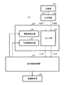
- FIG. 3 is a diagram illustrating a configuration example of the magnetic field measurement apparatus according to the second embodiment.
- the magnetic field measurement device 20 includes a light source unit 21, a light dividing unit 22, a sensor unit 25, a static magnetic field generation unit 26, an RF magnetic field generation unit 27, a signal control processing unit 24, and a magnetic field analysis unit 50.
- the light source unit 21 outputs light, and it is desirable to use the light source device 10 in the first embodiment, but it may not be used.
- the light splitting unit 22 splits the laser beam L21 output from the light source unit 21 into two laser beams L22 and L23.
- One sensor unit 25 that passes light output from the light source unit 21, a static magnetic field generation unit 26, and an RF magnetic field generation unit 27 are disposed in the magnetic field shield 23.
- the sensor unit 25 is applied with a static magnetic field by the static magnetic field generation unit 26 and an RF magnetic field by the RF magnetic field generation unit 27.
- a measurement target (not shown) is in the vicinity of the sensor unit 25, and a magnetic field by the measurement target is also applied.
- the laser beam L22 split by the light splitting unit 22 passes through the sensor unit 25, whereby the laser beam L24 having information on the magnetic field generated from the measurement target and fluctuations in light intensity derived from the sensor unit 25, that is, noise. It becomes.
- the laser beam L23 has a noise component derived from the sensor unit 25.
- the signal control processing unit 24 removes noise (light intensity fluctuation) derived from the sensor unit 25 from the electrical signal obtained from the laser beam L24 based on the laser beams L23 and L24 that have passed through the sensor unit 25. In addition, the signal control processing unit 24 sends an electrical signal necessary for the magnetic field analysis to the magnetic field analysis unit 50. Further, the signal control processing unit 24 supplies a constant current to the static magnetic field generation unit 26 and controls the frequency of the RF magnetic field in the RF magnetic field generation unit 27 based on the signal from which noise is removed. Then, the magnetic field analysis unit 50 performs magnetic field analysis based on the electric signal necessary for the magnetic field analysis sent from the signal control processing unit 24.
- the magnetic field analysis unit 50 may be a device different from the magnetic field measurement device 20.
- the magnetic field shield 23 is preferably made of permalloy having a high magnetic permeability. Further, the size of the magnetic field shield 23 depends on the measurement object. For example, when a biomagnetic field is measured from a human heart or brain, the size of the magnetic field shield 23 is a size that can cover the human body.
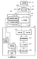
- FIG. 4 is a diagram illustrating a detailed configuration of the magnetic field measurement apparatus according to the second embodiment
- FIG. 5 is a diagram illustrating a detailed configuration of the sensor apparatus according to the second embodiment.
- the magnetic field measurement device 20 includes a light source device 201 that is a light source unit 21.
- the light source device 201 is preferably the light source device 10 in the first embodiment, but may not be so.
- the light splitting unit 22 includes, for example, a beam splitter 202 and a plurality of mirrors 203.
- the sensor device 211 is arranged inside the magnetic field shield 23 together with the generation source of the magnetic field to be measured. Further, inside the magnetic field shield 23, a static magnetic field is applied to the sensor glass cell 223 (FIG. 5) in the sensor device 211 in a direction that forms 45 degrees with the optical axis of the laser light input from the light source device 201. A static magnetic field generator 212 to be applied is arranged. Furthermore, an RF magnetic field generator 213 that generates an oscillating magnetic field in a direction orthogonal to the static magnetic field generated by the static magnetic field generator 212 is disposed inside the magnetic field shield 23.
- the RF magnetic field generator 213 is also a coil, like the static magnetic field generator 212, and is preferably a Helmholtz coil arranged so as to sandwich the sensor glass cell 223.
- the function of the RF magnetic field generator 213 is to supply an oscillating magnetic field whose RF frequency is precisely controlled by the oscillation circuit 237 of the signal control processing unit 24.
- the signal control processing unit 24 includes two photodetectors (conversion units) 231 and 232, a differential amplifier circuit (difference unit) 233, a filter circuit 234, a phase detection circuit 235, a loop filter circuit 236, and an oscillation circuit 237. Have. These functions will be described later.
- the signal control processing unit 24 includes a stabilized current source 238 that supplies a precisely controlled constant current to the static magnetic field generator 212.
- the sensor device 211 includes collimating lenses 221 and 225, a ⁇ / 4 wavelength plate (circular polarization unit) 222, a sensor glass cell 223, and condensing lenses 224 and 226.
- an alkali metal gas is sealed in the sensor glass cell 223.
- the laser beam L21 output from the light source device 201 is a laser beam including the wavelength of an alkali metal absorption line (D1 line or D2 line) sealed in the sensor glass cell 223.
- D1 line or D2 line alkali metal absorption line
- the laser beam L21 from the light source device 201 is separated into two laser beams L22 and L23 by the beam splitter 202 of the beam splitter 22 so as to have the same light intensity.
- the separated laser beams L22 and L23 are input to the sensor device 211 as laser beams that travel in parallel so as not to overlap each other by the mirror 203.
- the sensor glass cell 223 is provided in the subsequent stage of the ⁇ / 4 wavelength plate 222 and is filled with alkali metal gas, and is separated by the light splitting unit 22 (FIG. 4).
- Light (laser beams L22 and L23) is input.
- the laser beam L22 that is one of the two laser beams L22 and L23 that are input from the beam splitting unit 22 passes through a collimator lens 221 and a ⁇ / 4 wavelength plate 222. Is input to the glass cell 223 for use.
- the laser light L22 is converted into parallel light by the collimator lens 221 and is converted to circularly polarized laser light L24 by the ⁇ / 4 wavelength plate 222 and input to the sensor glass cell 223.
- the parallel light by the collimating lens 221 means light that does not diffuse and converge.
- the laser beam L23 is introduced into the sensor glass cell 223 via the collimator lens 225.
- the laser light L23 is converted into parallel light by the collimator lens 225, and is input to the sensor glass cell 223 in a non-polarized state.
- the laser beams L24 and L23 that have passed through the sensor glass cell 223 are condensed by the condenser lenses 224 and 226, respectively, and input to the photodetectors 231 and 232 of the signal control processing unit 24, respectively.
- the photodetectors 231 and 232 convert the intensity of each of the two lights (laser lights L24 and L23) that have passed through the sensor glass cell 223 into electrical signals.
- the laser beams L23 and L24 are input to the sensor glass cell 223 in a parallel state. Further, by outputting from the same light source device 201 (FIG. 4), the laser light L23 and L24 have the same wavelength and light intensity. As shown in FIG. 4, the electric signals output from the photodetectors 231 and 232 are respectively subjected to a difference in the differential amplifier circuit 233 and amplified to an appropriate gain. Here, the difference between the circularly polarized laser beam L24 and the non-polarized laser beam L23 is obtained by subtracting the electric signals from the photodetectors 231 and 232 by the differential amplifier circuit 233. .
- the non-polarized laser beam L23 is regarded as a laser beam having only a noise component. Therefore, the differential amplifier circuit 233 subtracts the electrical signal derived from the non-polarized laser beam L23 from the electrical signal derived from the circularly polarized laser beam L24. By doing in this way, the noise component in the laser beam L24 is removed. That is, the noise component derived from the sensor glass cell 223 is removed from the laser light L24.
- the electric signal output from the differential amplifier circuit 233 is adjusted to a band necessary for analysis by the filter circuit 234.
- the phase detection circuit 235 detects the electrical signal from the filter circuit 234 using the electrical signal from the oscillation circuit 237 as a reference signal.
- the loop filter circuit 236 performs control so that the detected electric signal does not oscillate. Further, when the signal output from the loop filter circuit 236 is input to the oscillation circuit 237, the oscillation frequency of the oscillation circuit 237 is voltage-controlled. Then, when the oscillation frequency of the oscillation circuit 237 is input to the RF magnetic field generator 213, the frequency of the RF magnetic field of the RF magnetic field generator 213 is feedback-controlled.
- the control of the RF magnetic field generator 213 by the phase detection circuit 235, the oscillation circuit 237, and the loop filter circuit 236 is a known technique.
- the magnetic field analysis part 50 measures the weak magnetic field generate
- one sensor unit 25 that passes light (laser light) output from the light source unit 21 and two lights (laser light) based on the light that has passed through the sensor unit 25.
- the fluctuation (noise) of the light intensity derived from the sensor section 25 can be removed by removing the fluctuation of the light intensity by taking the difference based on the light that has passed through the same sensor section 25. Thereby, a signal based on the light (laser light) can be stabilized.
- the light output from the same light source unit 21 it is possible to remove noise by light (laser light) having the same frequency and light intensity, stabilize the light (laser light) after noise removal, and Therefore, it is possible to eliminate the need to adjust the frequency and light intensity.
- the light source device 10 according to the first embodiment as the light source unit 21 (light source device 201), it is possible to have the same effect as the light source device 10 in the first embodiment.
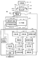
- FIG. 6 is a diagram illustrating a configuration example of a magnetic field measurement apparatus according to the third embodiment.
- the magnetic field measurement device 30 includes a light source unit 31, a light splitting unit 32, a sensor unit 35, a static magnetic field generation unit 36, an RF magnetic field generation unit 37, a signal control processing unit 34, a magnetic field analysis unit 50, and a light intensity control unit 39.
- the light source unit 31 outputs light, and it is desirable to use the light source device 20 in the first embodiment, but it may not be used.
- the light splitting unit 32 splits the laser beam L31 output from the light source unit 31 into two laser beams L32 and L33. That is, the light splitting unit 32 separates the laser light L31 transmitted from the same light source unit into the laser light L32 that is the first light and the laser light L33 that is the second light.
- the light intensity controller 39 converts the laser beam L31 into the laser beam L34 and outputs the laser beam L31 by intentionally superimposing a noise component on the laser beam L31 by a function described later. That is, the light intensity control unit 39 superimposes noise, which is a fluctuation of the electrical signal sent from the signal control processing unit 34, on the laser light L32 that is the first light.
- a sensor unit 35 In the magnetic field shield 33, a sensor unit 35, a static magnetic field generation unit 36, and an RF magnetic field generation unit 37 are arranged. Since the magnetic field shield 33 is the same as that of the second embodiment, detailed description thereof is omitted here.
- the sensor unit 35 is applied with a static magnetic field by the static magnetic field generation unit 36 and an RF magnetic field by the RF magnetic field generation unit 37.
- a measurement target (not shown) is in the vicinity of the sensor unit 35, and a magnetic field by the measurement target is also applied.
- the laser beam L34 becomes a laser beam L36 having information on the magnetic field generated from the measurement target and noise derived from the sensor unit 35.
- the laser beam L33 becomes a laser beam L33 having a noise component derived from the sensor unit 35.
- the signal control processing unit 34 sends a noise component in the laser light L33 to the light intensity control unit 39.
- the light intensity control unit 39 superimposes the transmitted noise component on the laser light L32 by controlling the light intensity of the laser light L32.
- the signal control processing unit 34 controls the frequency of the RF magnetic field to the RF magnetic field generation unit 37 based on the electric signal based on the laser beam L34. Further, the signal control processing unit 34 supplies a constant current to the static magnetic field generation unit 36. Further, the signal control processing unit 34 sends an electric signal necessary for the magnetic field analysis to the magnetic field analysis unit 50. Then, the magnetic field analysis unit 50 performs magnetic field analysis based on the electrical signal necessary for the magnetic field analysis sent from the signal control processing unit 34.
- the magnetic field analysis unit 50 may be a device different from the magnetic field measurement device 30.
- FIG. 7 is a diagram illustrating a detailed configuration of the magnetic field measurement apparatus according to the third embodiment
- FIG. 8 is a diagram illustrating a detailed configuration of the sensor apparatus according to the third embodiment.
- the magnetic field measurement device 30 includes a light source device 301 that is a light source unit 31.
- the light source device 301 is desirably the light source device 10 of the first embodiment, but it may not be so.
- the light splitting unit 32 includes a beam splitter 302 and a plurality of mirrors 303.
- the magnetic field measurement device 30 includes an acousto-optic modulator (acousto-optic modulator) 351 as the light intensity controller 39.
- the acousto-optic modulator 351 has the same properties as the acousto-optic modulator 121 in the first embodiment (FIG. 2).
- a sensor device 311 that is the sensor unit 35
- a static magnetic field generation device 312 that is a static magnetic field generation unit 36
- an RF magnetic field generation device 313 that is an RF magnetic field generation unit 37 are arranged. .
- the signal control processing unit 34 includes two photodetectors (conversion units) 331 and 341, a reference voltage circuit (reference voltage unit) 332, a differential amplifier circuit 333, an integration circuit 334, and a drive circuit (drive unit) 335. Have. Further, the signal control processing unit 34 includes an amplifier circuit 342, a filter circuit 343, a phase detection circuit 344, a loop filter circuit 345, and an oscillation circuit 346. These functions will be described later. The signal control processing unit 34 includes a stabilized current source 347 that supplies a precisely controlled constant current to the static magnetic field generator 312.
- the sensor device 311 includes collimator lenses 321 and 325, a ⁇ / 4 wavelength plate (circular polarization unit) 322, a sensor glass cell 323, and condenser lenses 324 and 326.
- the sensor glass cell 323 is provided at the rear stage of the ⁇ / 4 wavelength plate 322 and is filled with an alkali metal gas, and is a laser that is a circularly polarized first light.
- the laser beam L31 output from the light source device 301 is a laser beam including the wavelength of an alkali metal absorption line (D1 line or D2 line) sealed in the sensor glass cell 323 in the sensor apparatus 311.
- D1 line or D2 line an alkali metal absorption line
- the laser beam L31 from the light source device 301 is separated into two laser beams L32 and L33 by the beam splitter 302 so as to have the same light intensity.
- the separated laser beams L ⁇ b> 32 and L ⁇ b> 33 are input to the sensor device 311 as laser beams traveling in parallel so as not to overlap with each other by the mirror 303.
- the laser beam L32 is controlled in light intensity by the acousto-optic modulator 351, so that noise derived from the sensor glass cell 323 (FIG. 8) is superimposed on the laser beam L32.
- the laser beam L34 is obtained.
- the control of the light intensity by the acousto-optic modulator 351 will be described later.
- the laser beam L34 is input to the sensor glass cell 323 via the collimating lens 321 and the ⁇ / 4 wavelength plate 322.
- the laser light L32 is separated into zero-order light L34 and first-order light L35 by the acousto-optic modulator 351, and the zero-order light L34 is converted into parallel light by the collimator lens 321.
- the primary light L35 is not used for the same reason as the acousto-optic modulator 121 in the first embodiment.
- the zero-order light L34 is converted into circularly polarized laser light L36 by the ⁇ / 4 wavelength plate 322, and then input to the sensor glass cell 323.
- the laser beam L33 is input to the sensor glass cell 323 via the collimator lens 325 as canceling excitation light.
- the laser light L33 is converted into parallel light by the collimator lens 325, and is input to the sensor glass cell 323 in a non-polarized state.
- the laser beams L33 and L36 that have passed through the sensor glass cell 323 are condensed by the condenser lenses 326 and 324, and the light intensity is converted into electric signals by the photodetectors 331 and 341, respectively.
- the conditions under which the laser beams L33 and L36 are input to the sensor glass cell 323 are the same as in the second embodiment. That is, the conditions for the laser beams L33 and L36 to be input to the sensor glass cell 323 are that the wavelengths of the light are the same, the light intensities are the same, and they are input in parallel so as not to overlap.
- the electrical signal output from the photodetector 341 is amplified to an appropriate gain by the amplifier circuit 342 and adjusted to a band necessary for analysis by the filter circuit 343.
- the electrical signal output from the filter circuit 343 is used for frequency control of the RF magnetic field of the RF magnetic field generator 313 by the phase detection circuit 344, the loop filter circuit 345, and the oscillation circuit 346. Since the functions of the magnetic field analysis unit 50, the phase detection circuit 344, the loop filter circuit 345, and the oscillation circuit 346 are the same as those in the second embodiment, detailed description thereof is omitted here.
- the electric signal output from the photodetector 331 is differentiated from the reference voltage supplied from the reference voltage circuit 332 by the differential amplifier circuit 333 and amplified to an appropriate gain.
- the reference voltage is set in advance to a voltage that can extract only a noise component from the electrical signal output from the photodetector 331.
- the electric signal output from the differential amplifier circuit 333 becomes an electric signal including only noise components derived from the sensor glass cell 323 in the non-polarized laser light L33. Therefore, the electrical signal output from the differential amplifier circuit 333 is an electrical signal including only noise components derived from the sensor glass cell 323 (FIG. 8).
- the electrical signal output from the differential amplifier circuit 333 is controlled to a necessary band by the integration circuit 334 and then input to the drive circuit 335.
- the drive circuit 335 controls the voltage applied to the acousto-optic modulator 351 based on the electrical signal output from the integration circuit 334. That is, the drive circuit 335 applies the change in the voltage obtained by reversing the positive / negative of the fluctuation of the electric signal to the acousto-optic modulator 351.
- the drive circuit 335 controls the applied voltage of the acousto-optic modulator 351 based on the electrical signal obtained by reversing the sign of the electrical signal output from the integration circuit 334.
- the acousto-optic modulator 351 varies the light intensity of the laser light L32 with the same function as the acousto-optic modulator 121 in the first embodiment.
- the light (laser light) used for magnetic field measurement can be made one, so that The configuration of the magnetic field measurement device can be used. That is, the magnetic field measurement device 30 can be realized by adding the respective units 331 to 335 to the existing magnetic field measurement device.
- the units 331 to 335 and the units 341 to 347 may be separate devices.
- the acousto-optic modulator 351 is used as the light intensity control unit 39, settings such as frequency adjustment of light (laser light) output from the light source device 301 become unnecessary.
- the light source device 10 according to the first embodiment as the light source unit 21 (light source device 201), it is possible to have the same effect as the light source device 10 in the first embodiment.
- FIG. 9 is a diagram illustrating a configuration example of the magnetic field measurement apparatus according to the fourth embodiment.
- the magnetic field measurement apparatus 40 includes light source units 41 and 42, a sensor unit 45, a static magnetic field generation unit 46, a signal control processing unit 44, and a magnetic field analysis unit 50.
- the light source units 41 and 42 output the laser beams L41 and L42, and it is desirable to use the light source device 10 in the first embodiment, but it may not be used.
- a sensor unit 45 and a static magnetic field generation unit 46 are disposed in the magnetic field shield 43. Since the magnetic field shield 43 is the same as that in the second embodiment, the description thereof is omitted.
- a static magnetic field from a static magnetic field generator 46 is applied to the sensor unit 45.
- a measurement target (not shown) is in the vicinity of the sensor unit 45, and a magnetic field by the measurement target is also applied.
- the laser beam L41 output from the light source unit 41 passes through the sensor unit 45, and becomes laser beams L45 and L46 having information on the magnetic field generated from the measurement target.
- the laser beam L42 is used to spin-polarize the alkali metal in the sensor unit 45. These will be described later.
- the signal control processing unit 44 removes noise originating from the sensor unit 45 based on the laser beams L45 and L46 that have passed through the sensor unit 45. Further, the signal control processing unit 44 sends an electric signal necessary for the magnetic field analysis to the magnetic field analysis unit 50. Further, the signal control processing unit 44 supplies a constant current to the static magnetic field generation unit 46. Then, the magnetic field analysis unit 50 performs magnetic field analysis based on the electric signal necessary for the magnetic field analysis sent from the signal control processing unit 44.
- the magnetic field analysis unit 50 may be a device different from the magnetic field measurement device 40.
- the magnetic field shield 43 in which the sensor unit 45 and the static magnetic field generation unit 46 are arranged is the same as that in the second embodiment, the description thereof is omitted here.
- FIG. 10 is a diagram illustrating a detailed configuration of the magnetic field measurement apparatus according to the fourth embodiment
- FIG. 11 is a diagram illustrating a detailed configuration of the sensor apparatus according to the fourth embodiment.
- the magnetic field measurement device 40 includes two light source devices 401 and 402 that are light source units 41 and 42.
- the light source devices 401 and 402 are preferably the light source device 10 of the first embodiment, but they may not be. Further, only the light source device 401 may be the light source device 10 of the first embodiment.
- a sensor device 411 that is the sensor unit 45 and a static magnetic field generation device 412 that is a static magnetic field generation unit 46 are arranged in the magnetic field shield.
- the signal control processing unit 44 includes two photodetectors (conversion units) 431 and 432, a differential amplifier circuit 433, and a filter circuit 434. These functions will be described later.
- the sensor device 411 is arranged inside the magnetic field shield 43 together with a measurement target (not shown) that is a generation source of the measurement magnetic field.
- a static magnetic field generator 412 that applies a static magnetic field orthogonal to the optical axes of the laser light L41 and the laser light L42 is also arranged in the sensor device 411. .
- the static magnetic field generator 412 is a coil, and may be, for example, a Helmholtz coil or the like that is arranged so as to sandwich the sensor glass cell 423 in the sensor device 411.
- the static magnetic field generator 412 applies a stable static magnetic field from a stabilized current source 435 provided outside the magnetic field shield 43 to apply a stable static magnetic field to the sensor device 411.
- the sensor device 411 includes collimating lenses 421 and 424, a ⁇ / 2 wavelength plate (linear polarization portion) 422, a ⁇ / 4 wavelength plate (circular polarization portion) 425, a sensor glass cell 423, A polarization beam splitter (separation unit) 426 and condenser lenses 427 and 428 are included.
- an alkali metal gas is sealed in the sensor glass cell 423.
- the laser beam L41 output from the light source device 401 is a laser beam including the wavelength of an alkali metal absorption line (D1 line or D2 line) sealed in the sensor glass cell 423 (FIG. 11).
- the laser beam L42 output from the light source device 402 is a laser beam that does not include the wavelength of the alkali metal absorption line.
- the traveling directions of the laser light L41 and the laser light L42 are different by 90 degrees, and intersect at right angles in the sensor glass cell 423.
- the sensor glass cell 423 is provided in the subsequent stage of the ⁇ / 2 wavelength plate 422 and the ⁇ / 4 wavelength plate 425.
- the sensor glass cell 423 is filled with an alkali metal gas, and linearly polarized light (laser light L43) and circularly polarized light (laser light L44) are inputted orthogonally.
- the laser light L ⁇ b> 42 that is the second light output from the light source device 402 (FIG. 10) is converted into parallel light by the collimator lens 424, and then circularly polarized by the ⁇ / 4 wavelength plate 425.
- the laser light L44 is input to the sensor glass cell 423.
- the alkali metal atoms inside the sensor glass cell 423 are brought into a spin-polarized state by the circularly polarized laser beam L44.
- the laser light L41 (probe light) that is the first light output from the light source device 401 becomes parallel light by the collimator lens 421, and then becomes linearly polarized laser light L43 by the ⁇ / 2 wavelength plate 422. It inputs into the glass cell 423 for sensors.
- the linearly polarized laser beam L43 that has passed through the sensor glass cell 423 is separated by the polarization beam splitter 426 into a counterclockwise circularly polarized laser beam L45 and a clockwise circularly polarized laser beam L46.
- the counterclockwise circularly polarized laser beam L45 is collected by the condenser lens 427, and the counterclockwise circularly polarized laser beam L45 collected by the photodetector 431 is converted into an electric signal.
- the clockwise circularly polarized laser beam L46 is collected by the condenser lens 428, and the clockwise circularly polarized laser beam L46 collected by the photodetector 432 is detected and converted into an electrical signal.
- the electric signals output from the photodetectors 431 and 432 are subtracted by the differential amplifier circuit 433 and further amplified to an appropriate gain.
- the differential amplifier circuit 433 makes a difference between the electrical signal converted from the counterclockwise circularly polarized light (laser light L45) and the electrical signal converted from the clockwise circularly polarized light (laser light L46). To do.
- the differential amplifier circuit 433 the difference between the outputs from the photodetectors 431 and 432 is obtained, so that the difference between the counterclockwise circularly polarized laser light L45 and the clockwise circularly polarized laser light L46 is obtained. .
- the electric signal output from the differential amplifier circuit 433 is processed by the filter circuit 434 in order to extract a signal component of an appropriate signal band.
- the electric signal output from the filter circuit 434 reflects the inclination variation of the polarization plane of linearly polarized light corresponding to the magnetic field entering the sensor glass cell 423.
- the electrical signal output from the filter circuit 434 is analyzed by the magnetic field analysis unit 50.
- the system can be simplified in addition to the effects of the magnetic field measurement apparatus 20 in the second embodiment.
- the magnetic field measurement apparatus 20a detects the magnetic field applied to the sensor unit 25 by the inclination of the polarization plane of linearly polarized light. Therefore, the magnetic field measurement apparatus 20a shown in FIG. 12 has the light source unit 51 that outputs the laser light L51 separately from the light source unit 21. Further, the signal control processing unit 24a of the magnetic field measurement apparatus 20a has a configuration in which the phase detection circuit 235, the loop filter circuit 236, and the oscillation circuit 237 of FIG. 4 are omitted.
- the polarization beam splitter 426 is omitted from the configuration of FIG. 11, and the condensing lenses 427 and 428 and the photodetectors 431 and 432 are condensing lenses 224 and 226 of FIG. And the functions of the photodetectors 231 and 232.
- the laser beam L51 has the same function as the laser beam L42 in the fourth embodiment.
- the magnetic field measurement apparatus 30a detects the magnetic field applied to the sensor unit 35 by the inclination of the polarization plane of linearly polarized light. Therefore, the magnetic field measurement apparatus 30a shown in FIG. 13 has the light source unit 52 that outputs the laser light L52 separately from the light source unit 31. Further, the signal control processing unit 34a of the magnetic field measurement apparatus 30a has a configuration in which the phase detection circuit 344, the loop filter circuit 345, and the oscillation circuit 346 of FIG. 4 are omitted.
- the polarization beam splitter 426 is omitted from the configuration of FIG. 11, and the condensing lenses 427 and 428 and the photodetectors 431 and 432 are condensing lenses 324 and 326 of FIG. And the functions of the photodetectors 331 and 341.
- the laser beam L52 has the same function as the laser beam L42 in the fourth embodiment.
- an RF magnetic field analysis device may be added to the static magnetic field measurement device 40 in FIG. 9 of the third embodiment.
- the light source unit 42 is omitted
- the configuration of the sensor unit and the signal control processing unit is the configuration of the sensor unit and the signal processing unit in the second embodiment or the third embodiment.
- the introduction of the laser beams L22, L23, L24, L33, L34, L36, L41, L42, L43, and L44 into the sensor glass cells 223, 323, and 423 may be by spatial propagation, but light is considered in consideration of practicality. Introduction using fiber is preferred. At this time, it is desirable to use a polarization-maintaining optical fiber in consideration of the polarization state stability of the laser beams L23, L24, L33, L36, L42, and L43 that pass through the optical fiber.
- the spatially propagated light is used.
- Multi-mode optical fibers generally do not have a polarization plane preserving function.
- the polarization collapse which is a problem in the input to the sensor glass cells 223, 323, and 423, does not cause a problem when detecting light by the photodetectors 231, 232, 331, 341, 431, and 432. There is no problem with using fiber.
- a ⁇ / 4 wavelength plate and a ⁇ / 2 wavelength plate are inserted into the connection place between the polarization maintaining optical fiber used for introduction and the light source devices 201, 301, 401, 402, and the optical axis of the polarization maintaining optical fiber is inserted.
- the polarization plane may be adjusted and used.
- the present invention is not limited to the above-described embodiment, and includes various modifications.
- the above-described embodiment has been described in detail for easy understanding of the present invention, and is not necessarily limited to having all the configurations described.
- a part of the configuration of a certain embodiment can be replaced with the configuration of another embodiment, and the configuration of another embodiment can be added to the configuration of a certain embodiment.
- each of the above-described configurations 102, 117, 118, 125 to 127, 233 to 237, 333 to 335, and 342 to 346 is realized by hardware by designing a part or all of them with, for example, an integrated circuit. May be.
- Each of the above-described structures 102, 117, 118, 125 to 127, 233 to 237, 333 to 335, 342 to 346 is a program that a processor such as a CPU (Central Processing Unit) realizes each function.
- a processor such as a CPU (Central Processing Unit)
- control lines and information lines are those that are considered necessary for explanation, and not all control lines and information lines are necessarily shown on the product. In practice, it can be considered that almost all configurations are connected to each other.
- Light source device 11
- Laser output unit (light generation unit)
- DESCRIPTION OF SYMBOLS 12
- Frequency stabilization part 13
- Drive part 14
- Intensity stabilization part 20 30, 40
- Magnetic field measuring device 121,351
- Acoustooptic modulator (light intensity fluctuation correction part, acoustooptic modulation part) 130
- Light intensity fluctuation detection circuit (light intensity fluctuation detection unit) 21, 31, 41, 42 Light source unit 22, 32
- Light splitting unit 24, 34, 44
- Signal control processing unit 25, 35, 45
- Sensor unit 39
- Light intensity control unit 127 Drive circuit (light intensity fluctuation correcting unit, modulation driving unit) 222, 322, 425 ⁇ / 4 wave plate (circular polarization part) 223, 323, 423
- Sensor glass cells 231, 232, 331, 341, 431, 432
- Photodetectors conversion units
- 233, 333, 433 Difference amplifier circuit (difference unit)
- Reference voltage circuit (reference voltage section)
Landscapes
- Physics & Mathematics (AREA)
- General Physics & Mathematics (AREA)
- Optics & Photonics (AREA)
- Electromagnetism (AREA)
- Condensed Matter Physics & Semiconductors (AREA)
- Nonlinear Science (AREA)
- Engineering & Computer Science (AREA)
- Plasma & Fusion (AREA)
- Optical Modulation, Optical Deflection, Nonlinear Optics, Optical Demodulation, Optical Logic Elements (AREA)
- Investigating Or Analysing Materials By Optical Means (AREA)
Abstract
Description
その他の解決手段については、実施形態中で適宜説明する。
なお、本実施形態における各図において、破線矢印は光(レーザ光)を示し、実線矢印は、電気信号を示すものとする。また、本実施形態で示される光源装置や、磁場計測装置は、心磁計、脳磁計、筋磁計等の生体磁場計測装置や、磁性材料の物性測定等に用いられるものである。
図1は、第1実施形態に係る光源装置の概要構成例を示す図である。
光源装置10は、レーザ出力部(光発生部)11、周波数安定化部12、強度安定化部14及び駆動部13を有している。
レーザ出力部11は、電圧が印加されることでレーザ光L11を発生して出力する。
周波数安定化部12は、駆動部13を制御することで、レーザ出力部11が出力するレーザ光L11の周波数を安定化させる。
強度安定化部14は、周波数安定化部12から出力されたレーザ光L14の光強度を安定化させ、光強度が安定化しているレーザ光L17を出力する。なお、強度安定化部14は、周波数安定化部12の後段に別の構成として備えられていることが望ましい。このようにすることで、周波数安定化部12で周波数安定化を行ったレーザ光L14の光強度安定を行うことができ、周波数安定かつ光強度が安定しているレーザ光L17を出力することができる。
光源装置10は、レーザ出力部11としてのレーザ出力装置101と、駆動部13としての駆動回路102とを有している。
また、光源装置10は、周波数安定化部12の構成として、ビームスプリッタ111、ハーフミラー112、参照ガラスセル113、ND(Neutral Density)フィルタ114、ミラー115、光検出器116、位相検出回路117及び積分回路118を有する。各構成の機能は後記して説明する。ここで、参照ガラスセル113にはアルカリ金属ガスが封入されている。
レーザ出力装置101から出力されたレーザ光L11は、周波数安定化部12に入力し、周波数安定化が行われる。以下、周波数安定化部12の機能を説明するが、周波数安定化部12は既知の技術であるため、説明は簡単なものとする。
ここでは、レーザ光の周波数安定化の手法として、アルカリ金属の吸収線、もしくは干渉計を周波数安定化の基準として使用する手法を用いる。
まず、レーザ光L12は、参照ガラスセル113に封入されているアルカリ金属の吸収線を得るため、ハーフミラー112を経由してアルカリ金属のみが入った参照ガラスセル113を通過する。レーザ光L12は、参照ガラスセル113を通過する際、参照ガラスセル113内のアルカリ金属を励起する。従って、レーザ光L12はポンプ光とも称される。励起される際、レーザ光L12は特定の周波数成分が吸光される。
ミラー115で反射し、再度参照ガラスセル113に入力したレーザ光L12は、2回NDフィルタ114を通過することで、光強度が弱められる。ミラー115で反射し、再度参照ガラスセル113に入力したレーザ光L12をレーザ光L13と称する。レーザ光L13はプローブ光とも称される。なお、レーザ光L13は、レーザ光L12とは同一の光路を逆方向に進むことになる。
レーザ光L13は、参照ガラスセル113を通過後、ハーフミラー112で反射され、光検出器116に入力する。
続いて、積分回路118が位相検出回路117から出力された電気信号における高周波成分を除去した後、駆動回路102へ電気信号を出力する。
駆動回路102は、積分回路118から出力された電気信号を基に、周波数安定化部12から出力されたレーザ光L14の周波数制御を行う。
光強度が強いレーザ光L12(ポンプ光)は、参照ガラスセル113に封入されているアルカリ金属原子の励起を飽和する。このとき、参照ガラスセル113での光吸収周波数特性は、本来なら吸収線が現れるはずであるが、アルカリ金属原子の揺動等により、幅の広い吸収スペクトルが現れる。この吸収スペクトルのピーク値に周波数がロックされることで、周波数の安定化を図ることも可能であるが、ここでは、より正確を期すためレーザ光L13(プローブ光)が使用される。
その結果、レーザ光L13(プローブ光)のスペクトル特性において、前記した幅の広い吸収スペクトル中に、レーザ光L14による鋭い非吸収スペクトルが生じる。この非吸収スペクトルに、周波数がロックされることで、正確な周波数安定化が行われる。
次に、強度安定化部14による光強度安定処理について説明する。なお、周波数安定化部12による周波数安定処理と、強度安定化部14による光強度の安定化処理は、並行して行われる。
ビームスプリッタ111で分離され、強度安定化部14に道かれたレーザ光L14は、音響光学変調器121に入力する。このレーザ光L14は音響光学変調器121から出力される際にブラッグ回折によって、0次光、1次光、・・・、N次光(Nは整数)に分離されたレーザ光となって出射する。一般的には、0次光L15と、1次光L16との2つのレーザ光が分離される。
音響光学変調器121には、電圧が印加可能となっており、電圧が音響光学変調器121に印加されると、音響光学変調器121内部の音響光学素子に密着している圧電素子が、印加された電圧に応じた所定の振動数で振動する。この振動は、音響光学素子に伝達し、音響光学素子そのものも当該振動数で振動する。
さらに、音響光学変調器121に入力されたレーザ光L14の光強度をAとし、音響光学変調器121から出力される0次光L15の光強度をA0、1次光L16の光強度をA1とすると、A=A0+A1の関係が成り立つ。そして、A0、A1の値は、音響光学変調器121に印加される電圧によって調整可能である(ただし、A=A0+A1の関係は維持される)。このような性質は、一般に音響光学効果と呼ばれる。
前記したように、周波数安定部によって周波数を安定化したレーザ光L14が音響光学変調器121に入力すると、0次光L15及び1次光L16が出力される。
その際に、1次光L16の光強度が最大となるよう、音響光学変調器121に入力するレーザ光L14の角度(ブラッグアングル)を調節することが望ましい。このとき、入力するレーザ光L14の角度調節のため、音響光学変調器121に3軸(X軸、Y軸、Z軸)かつ角度(θ軸)等の位置調節機構があると容易に調整が可能となる。
音響光学変調器121からの0次光L15はビームスプリッタ122によって、強度安定化制御を行うためのレーザ光L18と、磁場計測に用いられるレーザ光L17(センサ励起光)の2つに分離される。
レーザL18光は、光検出器123に入力される。光検出器123は、入力された制御用レーザ光の光強度を電気信号に変換する。
続いて、積分回路126が、差動増幅回路125から出力される電圧変動のうち、所定の周波数以上の成分をカットする。つまり、積分回路126はローパスフィルタの機能を有する。
そして、駆動回路127が、積分回路126から出力された電圧を基に、音響光学変調器121に印加する電圧を変更する。具体的には、駆動回路127は、入力された電圧(積分回路126から出力された電圧)が+V1であれば、音響光学変調器121に印加する電圧をV1だけ下げる。逆に、入力された電圧が-V1であれば、駆動回路127は、音響光学変調器121に印加する電圧をV1だけ上げる。
音響光学変調器121は、印加される電圧に応じて0次光であるレーザ光L15の強度を変更する。すなわち、音響光学変調器121は、音響光学効果によってレーザ出力装置101から出力され、周波数安定化されたレーザ光L14を変更可能である。
つまり、駆動回路127は、光強度変動検出回路130が検出した光強度の変動を基に、音響光学変調器121に印加される電圧を制御することで、音響光学変調器121を駆動する。
以上のことが行われることにより、音響光学変調器121は、レーザ出力装置101から出力され、周波数安定化されたレーザ光L14を入力して、音響光学効果により入力したレーザ光L14の強度を変調し、0次光として出力する。
このように、光源装置10は、レーザ出力装置101から出力された光が、音響光学変調器121に入力され、音響光学変調器121から出力される0次光を出力している。さそして、光強度変動検出回路130は、音響光学変調器121から出力される0次光を基に、光の強度の変動を検出している。
これにより、音響光学変調器121に印加される電圧が一定となり、0次光L15の光強度が一定となる。
また、第1実施形態による光強度安定化処理は、実際の光(レーザ光)の光強度を基に行われるため、物理的な振動による光強度変動も除去可能である。物理的な振動とは、例えば、光源装置10が設置してある台が振動すること等である。
次に、磁場計測装置について説明する。
《第2実施形態》
図3~図5を参照して、本発明の第2実施形態に係る磁場計測装置について説明する。
第2実施形態に係る磁場計測装置20は、RF磁場で生じる光-RF二重共鳴を利用してセンサ部25に印加される磁場を検出するものである。
図3は、第2実施形態に係る磁場計測装置の構成例を示す図である。
磁場計測装置20は、光源部21、光分割部22、センサ部25、静磁場発生部26、RF磁場発生部27、信号制御処理部24及び磁場解析部50を有する。
光源部21は、光を出力するものであり、第1実施形態における光源装置10を用いることが望ましいが、用いられなくてもよい。
光分割部22は、光源部21から出力されたレーザ光L21を、レーザ光L22,L23の2つに分離する。
センサ部25には、静磁場発生部26による静磁場、RF磁場発生部27によるRF磁場が印加されている。また、測定対象(不図示)がセンサ部25の近傍にあり、測定対象による磁場も印加されている。
光分割部22によって、分割されたレーザ光L22はセンサ部25を通過することで、測定対象から生じる磁場の情報と、センサ部25に由来する光強度の変動、すなわちノイズとを有するレーザ光L24となる。なお、レーザ光L23はセンサ部25に由来するノイズ成分を有する。これらについては、後記して説明する。
そして、磁場解析部50は信号制御処理部24から送られる、磁場解析に必要な電気信号を基に磁場解析を行う。なお、磁場解析部50は、磁場計測装置20とは別の装置としてもよい。
図4は、第2実施形態に係る磁場計測装置の詳細な構成を示す図であり、図5は、第2実施形態に係るセンサ装置の詳細な構成を示す図である。
図4に示すように、磁場計測装置20は、光源部21である光源装置201を有している。前記したように、光源装置201は、第1実施形態における光源装置10が好ましいが、そうでなくてもよい。
そして、光分割部22は、例えば、ビームスプリッタ202と、複数のミラー203を有している。
そして、信号制御処理部24は、静磁場発生装置212に対し精密に制御された定電流を供給する安定化電流源238を有する。
光源装置201から出力されるレーザ光L21は、センサ用ガラスセル223に封入されているアルカリ金属の吸収線(D1線もしくはD2線)の波長を含むレーザ光である。
図5に示すように、光分割部22から入力される2つのレーザ光L22,L23のうち、一方のレーザ光であるレーザ光L22は、コリメートレンズ221、λ/4波長板222を介してセンサ用ガラスセル223に入力される。
レーザ光L22は、コリメートレンズ221で平行光となり、λ/4波長板222で円偏光のレーザ光L24となってセンサ用ガラスセル223に入力される。コリメートレンズ221による平行光とは、拡散及び収束しない光という意味である。
図4に示すように、光検出器231,232それぞれから出力される電気信号は、差動増幅回路233において差分され・適切なゲインに増幅される。
ここで、差動増幅回路233によって、光検出器231,232それぞれからの電気信号が差分されることで、円偏光であるレーザ光L24から無偏光のレーザ光L23の差分がとられることになる。
一方、位相検出回路235は、発振回路237からの電気信号を参照信号としてフィルタ回路234からの電気信号を検出する。ループフィルタ回路236は、検出された電気信号が発振しないように制御する。さらに、ループフィルタ回路236から出力された信号が発振回路237に入力されることで、発振回路237の発振周波数が電圧制御される。
そして、発振回路237の発信周波数がRF磁場発生装置213に入力されることで、RF磁場発生装置213のRF磁場の周波数がフィードバック制御される。なお、位相検出回路235、発振回路237、ループフィルタ回路236によるRF磁場発生装置213の制御は既知の技術である。
そして、磁場解析部50が、フィードバック制御時のループフィルタ回路236の出力変化から、センサ用ガラスセル223の近傍の測定対象で発生する微弱磁場を計測する。
図6~図8を参照して、本発明の第3実施形態に係る磁場計測装置について説明する。
第3実施形態に係る磁場計測装置は、第2実施形態と同様にRF磁場で生じる光-RF二重共鳴を利用してセンサ部35に印加される測定対象の磁場を検出するものである。
図6は、第3実施形態に係る磁場計測装置の構成例を示す図である。
磁場計測装置30は、光源部31、光分割部32、センサ部35、静磁場発生部36、RF磁場発生部37、信号制御処理部34、磁場解析部50及び光強度制御部39を有する。
光源部31は、光を出力するものであり、第1実施形態における光源装置20を用いることが望ましいが、用いられなくてもよい。
光分割部32は、光源部31から出力されたレーザ光L31を、レーザ光L32,L33の2つに分離する。つまり、光分割部32は、同一の前記光源部から発信させたレーザ光L31を、第1の光であるレーザ光L32及び第2の光であるレーザ光L33に分離する。
光強度制御部39は、後記する機能によって、レーザ光L31にノイズ成分を意図的に重畳することで、レーザ光L31をレーザ光L34に変換し、出力する。つまり、光強度制御部39は、信号制御処理部34から送られた電気信号の変動であるノイズを第1の光であるレーザ光L32に重畳する。
磁場シールド33は、第2実施形態と同様であるので、ここでは詳細な説明を省略する。
センサ部35には、静磁場発生部36による静磁場、RF磁場発生部37によるRF磁場が印加されている。また、測定対象(不図示)がセンサ部35の近傍にあり、測定対象による磁場も印加されている。
レーザ光L34はセンサ部35を通過することで、測定対象から生じる磁場の情報と、センサ部35に由来するノイズとを有するレーザ光L36となる。なお、レーザ光L33はセンサ部35に由来するノイズ成分を有するレーザ光L33となる。これらについては、後記して説明する。
また、信号制御処理部34は、磁場解析に必要な電気信号を磁場解析部50へ送る。
そして、磁場解析部50は信号制御処理部34から送られる、磁場解析に必要な電気信号を基に磁場解析を行う。なお、磁場解析部50は磁場計測装置30とは別の装置としてもよい。
図7は、第3実施形態に係る磁場計測装置の詳細な構成を示す図であり、図8は、第3実施形態に係るセンサ装置の詳細な構成を示す図である。
図7に示すように、磁場計測装置30は、光源部31である光源装置301を有している。前記したように、光源装置301は第1実施形態の光源装置10であることが望ましいが、そうでなくてもよい。
そして、光分割部32は、ビームスプリッタ302と、複数のミラー303を有している。
また、磁場計測装置30は、光強度制御部39として音響光学変調器(音響光学変調部)351を有している。音響光学変調器351は、第1実施形態(図2)における音響光学変調器121と同様の性質を有するものである。
さらに、磁場シールド33内には、センサ部35であるセンサ装置311と、静磁場発生部36である静磁場発生装置312と、RF磁場発生部37であるRF磁場発生装置313が配置されている。
そして、信号制御処理部34は、静磁場発生装置312に対し精密に制御された定電流を供給する安定化電流源347を有する。
ここで、図8に示すように、センサ用ガラスセル323は、λ/4波長板322の後段に備えられるとともに、アルカリ金属ガスが封入されており、円偏光された第1の光であるレーザ光L36及び第2の光であるレーザ光L33が通過するものである。
光源装置301から出力されるレーザ光L31は、センサ装置311におけるセンサ用ガラスセル323に封入されているアルカリ金属の吸収線(D1線もしくはD2線)の波長を含むレーザ光である。
レーザ光L33,L36がセンサ用ガラスセル323に入力する条件は第2実施形態と同様である。つまり、レーザ光L33,L36がセンサ用ガラスセル323に入力する条件は、光の波長が同じであり、光強度が同じであり、重ならないように平行に入力することである。
また、フィルタ回路343から出力された電気信号は、位相検出回路344、ループフィルタ回路345、発振回路346によって、RF磁場発生装置313のRF磁場の周波数制御に用いられる。磁場解析部50、位相検出回路344、ループフィルタ回路345、発振回路346の機能は、第2実施形態と同様であるので、ここでは、詳細な説明を省略する。
従って、差動増幅回路333から出力された電気信号は、センサ用ガラスセル323(図8)に由来するノイズ成分のみを含む電気信号となる。
駆動回路335は、積分回路334から出力された電気信号に基づいて、音響光学変調器351の印加電圧を制御する。つまり、駆動回路335は、電気信号の変動の正負を逆転させた前記電圧の変化を前記音響光学変調器351に印加する。このとき、駆動回路335は、積分回路334から出力された電気信号の正負を逆転させた電気信号に基づいて、音響光学変調器351の印加電圧を制御する。
音響光学変調器351は、第1実施形態における音響光学変調器121と同様の機能により、レーザ光L32の光強度を変動させる。
λ/4波長板322で円偏光されたレーザ光L36がセンサ用ガラスセル323に入力すると、レーザ光L36における正負が逆転したノイズ成分と、センサ用ガラスセル323に由来するノイズとがキャンセルし合う。結果として、センサ用ガラスセル323を通過したレーザ光L36はセンサ用ガラスセル323由来のノイズ成分が除去されたものとなる。
また、光強度制御部39として音響光学変調器351が用いられることによって、光源装置301から出力される光(レーザ光)の周波数調整等の設定が不要となる。
図9~図11を参照して、本発明の第4実施形態に係る磁場計測装置について説明する。
第4実施形態に係る磁場計測装置40では、直線偏光の偏光面の傾きでセンサ部45に印加される磁場を検出する。
図9は、第4実施形態に係る磁場計測装置の構成例を示す図である。
磁場計測装置40は、光源部41,42、センサ部45、静磁場発生部46、信号制御処理部44及び磁場解析部50を有する。
光源部41,42は、レーザ光L41,L42を出力するものであり、第1実施形態における光源装置10を用いることが望ましいが、用いられなくてもよい。
磁場シールド43は、第2実施形態におけるものと同様のものであるので、説明を省略する。
センサ部45には、静磁場発生部46による静磁場が印加されている。また、測定対象(不図示)がセンサ部45の近傍にあり、測定対象による磁場も印加されている。
光源部41から出力されたレーザ光L41はセンサ部45を通過することで、測定対象から生じる磁場の情報を有するレーザ光L45,L46となる。なお、レーザ光L42はセンサ部45におけるアルカリ金属をスピン偏極させるために用いられる。これらについては、後記して説明する。
そして、磁場解析部50は信号制御処理部44から送られる、磁場解析に必要な電気信号を基に磁場解析を行う。磁場解析部50は磁場計測装置40とは別の装置としてもよい。
図10は、第4実施形態に係る磁場計測装置の詳細な構成を示す図であり、図11は、第4実施形態に係るセンサ装置の詳細な構成を示す図である。
図10に示すように、磁場計測装置40は、光源部41,42である2つの光源装置401,402を有している。前記したように光源装置401,402は第1実施形態の光源装置10であることが望ましいが、そうでなくてもよい。また、光源装置401のみが第1実施形態の光源装置10でもよい。
さらに、磁場シールド内には、センサ部45であるセンサ装置411と、静磁場発生部46である静磁場発生装置412が配置されている。
光源装置401(図10)から出力されるレーザ光L41は、センサ用ガラスセル423(図11)に封入されているアルカリ金属の吸収線(D1線もしくはD2線)の波長を含むレーザ光である。また、光源装置402から出力されるレーザ光L42は当該アルカリ金属の吸収線の波長を含まないレーザ光である。図11に示すように、レーザ光L41とレーザ光L42との進行方向は90度異なり、センサ用ガラスセル423内で直交交差する。つまり、センサ用ガラスセル423は、λ/2波長板422及びλ/4波長板425の後段に備えられている。そして、センサ用ガラスセル423は、アルカリ金属ガスが封入され、直線偏光された光(レーザ光L43)と、円偏光された光(レーザ光L44)とが直交して入力するものである。
同様に、右回りの円偏光のレーザ光L46は集光レンズ428で集光され、光検出器432が集光した右回りの円偏光のレーザ光L46を電気信号に検出変換する。
差動増幅回路433において、光検出器431,432それぞれからの出力の差分がとられることで、左回りの円偏光のレーザ光L45と、右回りの円偏光のレーザ光L46の差分がとられる。これにより、互いに逆向きの円偏光の差分がとられることにより、左回りの円偏光のレーザ光L45と右回りの円偏光のレーザ光L46とにおけるノイズは互いに打ち消しあい、センサ用ガラスセル423に由来するノイズがキャンセルされる。
そして、フィルタ回路434から出力された電気信号は、磁場解析部50によって解析される。
なお、図12に示すように第2実施形態の図3における磁場計測装置20からRF磁場計測部27が省略された磁場計測装置20aとしてもよい。ここで、磁場計測装置20aは、直線偏光の偏光面の傾きでセンサ部25に印加される磁場を検出する。従って、図12に示す磁場計測装置20aでは、光源部21とは別に、レーザ光L51を出力する光源部51を有している。
また、磁場計測装置20aの信号制御処理部24aでは、図4の位相検出回路235、ループフィルタ回路236、発振回路237が省略された構成となっている。
そして、磁場計測装置20aのセンサ部25aの構成は、図11の構成から偏光ビームスプリッタ426が省略され、集光レンズ427,428及び光検出器431,432が図5の集光レンズ224,226及び光検出器231,232の機能を有するものである。
ここで、レーザ光L51は、第4実施形態におけるレーザ光L42と同様の機能を有する。
また、磁場計測装置30aの信号制御処理部34aでは、図4の位相検出回路344、ループフィルタ回路345、発振回路346が省略された構成となっている。
そして、磁場計測装置30aのセンサ部35aの構成は、図11の構成から偏光ビームスプリッタ426が省略され、集光レンズ427,428及び光検出器431,432が図8の集光レンズ324,326及び光検出器331,341の機能を有するものである。
ここで、レーザ光L52は、第4実施形態におけるレーザ光L42と同様の機能を有する。
この場合、光源部42が省略され、センサ部、信号制御処理部の構成は、第2実施形態又は第3実施形態におけるセンサ部、信号処理部の構成となる。
以上のことは、第1実施形態の参照ガラスセル113でも同様である。
また、各実施形態において、制御線や情報線は説明上必要と考えられるものを示しており、製品上必ずしもすべての制御線や情報線を示しているとは限らない。実際には、ほとんどすべての構成が相互に接続されていると考えてよい。
11 レーザ出力部(光発生部)
12 周波数安定化部
13 駆動部
14 強度安定化部
20,30,40 磁場計測装置
121,351 音響光学変調器(光強度変動補正部,音響光学変調部)
130 光強度変動検出回路(光強度変動検出部)
21,31,41,42 光源部
22,32 光分割部
24,34,44 信号制御処理部
25,35,45 センサ部
39 光強度制御部
127 駆動回路(光強度変動補正部,変調駆動部)
222,322,425 λ/4波長板(円偏光部)
223,323,423 センサ用ガラスセル
231,232,331,341,431,432 光検出器(変換部)
233,333,433 差分増幅回路(差分部)
332 基準電圧回路(基準電圧部)
335 駆動回路(駆動部、光強度変動補正部)
422 λ/2波長板(直線偏光部)
426 偏光ビームスプリッタ(分離部)
Claims (14)
- 電圧が印加されることで光を発生して出力する光発生部と、
前記光発生部が出力している光の強度の変動を検出する光強度変動検出部と、
前記光強度変動検出部が検出した前記光の強度の変動を基に、前記光発生部が出力する光の強度が一定となるよう補正する光強度変動補正部と、
を有することを特徴とする光源装置。 - 前記光強度変動補正部は、前記光発生部から出力される光の強度を音響光学効果により変更可能な音響光学変調部と、前記音響光学変調部を駆動する変調駆動部と、を含んでおり、
前記音響光学変調部は、前記光発生部から出力される光を入力して、前記音響光学効果により前記入力した光の強度を変調し、0次光として出力し、
前記光強度変動検出部は、前記音響光学変調部から出力される前記0次光を基に、前記光の強度の変動を検出し、
前記変調駆動部は、前記光強度変動検出部が検出した前記光の強度の変動を基に、前記音響光学変調部に印加される電圧を制御する
ことを特徴とする請求項1に記載の光源装置。 - 前記光源装置は、前記光発生部が出力する光の周波数を安定させる周波数安定化部をさらに有する
ことを特徴とする請求項1に記載の光源装置。 - 前記光強度変動検出部及び前記光強度変動補正部は、前記周波数安定化部の後段に備えられる
ことを有する請求項3に記載の光源装置。 - 電圧が印加されることで光を発生して出力する光発生部と、
前記光発生部から出力される光の強度を音響光学効果により変更可能な音響光学変調部と、
前記音響光学変調部から出力される前記0次光を基に、前記光の強度の変動を検出する光強度変動検出部と、
前記光強度変動検出部が検出した前記光の強度の変動を基に、前記光強度変動検出部が検出した前記光の強度の変動を基に、前記音響光学変調部に印加される電圧を制御することで、前記光発生部が出力する光の強度が一定となるよう補正する変調駆動部と、
を有し、
前記音響光学変調部は、前記光発生部から出力される光を入力して、前記音響光学効果により前記入力した光の強度を変調し、0次光として出力する
ことを有することを特徴とする光源装置。 - 光源部から出力された光を通過させる1つのセンサ部と、
前記センサ部を通過した2つの光を基に、光の強度の変動を除去する信号制御処理部と、
を有することを特徴とする磁場計測装置。 - 前記磁場計測装置は、
同一の前記光源部から発信させた光を、2つの光に分離する光分割部
を、さらに有し、
前記センサ部は、
前記2つに分けられた光のうち、一方の光を円偏光させる円偏光部と、
前記円偏光部の後段に備えられるとともに、アルカリ金属ガスが封入されており、前記光分割部によって分離された2つの光が入力するセンサ用ガラスセルと、
を有し、
前記信号制御処理部は、
前記センサ用ガラスセルを通過した2つの光それぞれの強度を電気信号に変換する変換部と、
変換された前記電気信号を差分する差分部
を有することを特徴とする請求項6に記載の磁場計測装置。 - 前記磁場計測装置は、
同一の前記光源部から発信させた光を、第1の光及び第2の光に分離する光分割部と、
前記信号制御処理部から送られた電気信号の変動を前記第1の光に重畳する光強度制御部と、
を、更に有し、
前記センサ部は、
前記第1の光を円偏光させる円偏光部と、
前記円偏光部の後段に備えられるとともに、アルカリ金属ガスが封入されており、前記第1の光及び第2の光が通過するセンサ用ガラスセルと、
を有し、
前記信号制御処理部は、
前記センサ用ガラスセルを通過した前記第2の光の強度を電気信号に変換する変換部と、
基準電圧を供給する基準電圧部と、
前記変換部によって変換された電圧と、前記基準電圧との差分値を算出する差分部と、
前記差分値の変動を、前記電気信号の変動として前記光強度制御部へ送る駆動部と、
を有することを特徴とする請求項6に記載の磁場計測装置。 - 前記光強度制御部は、電圧が印加されることで、出力される光の強度を変更可能な音響光学変調部であり、
前記駆動部は、前記電気信号の変動の正負を逆転させた前記電圧の変化として前記音響光学変調部に印加する
ことを特徴とする請求項8に記載の磁場計測装置。 - 前記2つの光は、異なる前記光源部から出力され、
前記センサ部は、
前記2つの光のうち、第1の光を直線偏光させる直線偏光部と、
前記2つの光のうち、第2の光を円偏光させる円偏光部と、
前記直線偏光部及び前記円偏光部の後段に備えられるとともに、アルカリ金属ガスが封入され、前記直線偏光された光と、前記円偏光された光とが直交して入力するセンサ用ガラスセルと、
前記センサ用ガラスセルを通過した、前記第1の光を、右回りの円偏光の光と、左回りの円偏光の光とに分離する分離部と、
を有し、
前記信号制御部は、
前記左回りの円偏光の光及び右周りの円偏光の光それぞれを電気信号に変換する変換部と、
前記右回りの円偏光の光が変換された電気信号と、前記左周りの円偏光の光が変換された電気信号とを差分する差分部を
有する
ことを特徴とする請求項6に記載の磁場計測装置。 - 前記光源部は、
電圧が印加されることで光を発生して出力する光発生部と、
前記光発生部が出力している光の強度の変動を検出する光強度変動検出部と、
前記光強度変動検出部が検出した前記光の強度の変動を基に、前記光発生部が出力する光の強度が一定となるよう補正する光強度変動補正部と、
を有することを特徴とする請求項6に記載の磁場計測装置。 - 前記光強度変動補正部は、前記光発生部から出力される光の強度を音響光学効果により変更可能な音響光学変調部と、前記音響光学変調部を駆動する変調駆動部と、を含んでおり、
前記音響光学変調部は、前記光発生部から出力される光を入力して、前記音響光学効果により前記入力した光の強度を変調し、0次光として出力し、
前記光強度変動検出部は、前記音響光学変調部から出力される前記0次光を基に、前記光の強度の変動を検出し、
前記変調駆動部は、前記光強度変動検出部が検出した前記光の強度の変動を基に、前記音響光学変調部に印加される電圧を制御する
ことを特徴とする請求項11に記載の磁場計測装置。 - 前記光源部は、
前記光発生部が出力する光の周波数を安定させる周波数安定化部をさらに有する
ことを特徴とする請求項11に記載の磁場計測装置。 - 前記光強度変動検出部及び前記光強度変動補正部は、前記周波数安定化部の後段に備えられる
ことを有する請求項13に記載の磁場計測装置。
Priority Applications (3)
| Application Number | Priority Date | Filing Date | Title |
|---|---|---|---|
| JP2015551321A JP6300381B2 (ja) | 2013-12-03 | 2013-12-03 | 磁場計測装置 |
| PCT/JP2013/082494 WO2015083242A1 (ja) | 2013-12-03 | 2013-12-03 | 光源装置及び磁場計測装置 |
| US15/100,801 US10215816B2 (en) | 2013-12-03 | 2013-12-03 | Magnetic field measuring apparatus |
Applications Claiming Priority (1)
| Application Number | Priority Date | Filing Date | Title |
|---|---|---|---|
| PCT/JP2013/082494 WO2015083242A1 (ja) | 2013-12-03 | 2013-12-03 | 光源装置及び磁場計測装置 |
Publications (1)
| Publication Number | Publication Date |
|---|---|
| WO2015083242A1 true WO2015083242A1 (ja) | 2015-06-11 |
Family
ID=53273039
Family Applications (1)
| Application Number | Title | Priority Date | Filing Date |
|---|---|---|---|
| PCT/JP2013/082494 Ceased WO2015083242A1 (ja) | 2013-12-03 | 2013-12-03 | 光源装置及び磁場計測装置 |
Country Status (3)
| Country | Link |
|---|---|
| US (1) | US10215816B2 (ja) |
| JP (1) | JP6300381B2 (ja) |
| WO (1) | WO2015083242A1 (ja) |
Cited By (4)
| Publication number | Priority date | Publication date | Assignee | Title |
|---|---|---|---|---|
| EP3646782A1 (en) | 2018-11-02 | 2020-05-06 | Ricoh Company, Ltd. | Biomagnetic-field measurement apparatus, biomagnetic-field measurement method, and magnetic shield box |
| CN111755556A (zh) * | 2019-03-27 | 2020-10-09 | 中国科学院物理研究所 | 基于p-n结的高灵敏度光强起伏探测器 |
| CN111750987A (zh) * | 2019-03-27 | 2020-10-09 | 中国科学院物理研究所 | 基于肖特基结的高灵敏度光强起伏探测器 |
| JP2023553632A (ja) * | 2020-12-17 | 2023-12-25 | ノースロップ グラマン システムズ コーポレーション | エレクトロメータのセンサ制御システム |
Families Citing this family (55)
| Publication number | Priority date | Publication date | Assignee | Title |
|---|---|---|---|---|
| US9857441B2 (en) * | 2013-06-20 | 2018-01-02 | Honeywell International Inc. | Single beam radio frequency atomic magnetometer |
| US10162021B2 (en) * | 2013-08-02 | 2018-12-25 | Hitachi, Ltd. | Magnetic field measurement device |
| JP2016080613A (ja) * | 2014-10-21 | 2016-05-16 | セイコーエプソン株式会社 | 磁気計測装置、ガスセル、磁気計測装置の製造方法、およびガスセルの製造方法 |
| US10495943B2 (en) | 2016-11-03 | 2019-12-03 | Harris Corporation | Multi-channel phase-capable acousto-optic modulator (AOM) including beam stabilizer and related methods |
| US10754223B2 (en) | 2016-11-03 | 2020-08-25 | Harris Corporation | Multi-channel laser system including an acoustic-optic modulator (AOM) with atom trap and related methods |
| US10466516B2 (en) | 2016-11-03 | 2019-11-05 | Harris Corporation | Control system including a beam stabilizer and a phase modulation capable acousto-optic modulator for diverting laser output intensity noise to a first order laser light beam and related methods |
| US10509245B2 (en) | 2016-11-03 | 2019-12-17 | Harris Corporation | Multi-channel laser system including an acousto-optic modulator (AOM) with beam stabilizer and related methods |
| US9958711B1 (en) * | 2016-11-03 | 2018-05-01 | Harris Corporation | Control system using a phase modulation capable acousto-optic modulator for diverting laser output intensity noise to a first order laser light beam and related methods |
| US10782368B2 (en) | 2017-05-31 | 2020-09-22 | Northrop Grumman Systems Corporation | Pulsed-beam atomic magnetometer system |
| US10823790B2 (en) * | 2017-05-31 | 2020-11-03 | Northrop Grumman Systems Corporation | Pulsed-beam atomic magnetometer system |
| WO2019060298A1 (en) | 2017-09-19 | 2019-03-28 | Neuroenhancement Lab, LLC | METHOD AND APPARATUS FOR NEURO-ACTIVATION |
| US10809342B2 (en) | 2017-10-02 | 2020-10-20 | Northrop Grumman Systems Corporation | Calibration of a magnetometer system |
| US11717686B2 (en) | 2017-12-04 | 2023-08-08 | Neuroenhancement Lab, LLC | Method and apparatus for neuroenhancement to facilitate learning and performance |
| US11318277B2 (en) | 2017-12-31 | 2022-05-03 | Neuroenhancement Lab, LLC | Method and apparatus for neuroenhancement to enhance emotional response |
| US12280219B2 (en) | 2017-12-31 | 2025-04-22 | NeuroLight, Inc. | Method and apparatus for neuroenhancement to enhance emotional response |
| US11364361B2 (en) | 2018-04-20 | 2022-06-21 | Neuroenhancement Lab, LLC | System and method for inducing sleep by transplanting mental states |
| CN112074370B (zh) * | 2018-06-05 | 2023-03-14 | 伊雷克托科学工业股份有限公司 | 激光加工设备、其操作方法以及使用其加工工件的方法 |
| US10976386B2 (en) | 2018-07-17 | 2021-04-13 | Hi Llc | Magnetic field measurement system and method of using variable dynamic range optical magnetometers |
| US11136647B2 (en) | 2018-08-17 | 2021-10-05 | Hi Llc | Dispensing of alkali metals mediated by zero oxidation state gold surfaces |
| WO2020036666A1 (en) | 2018-08-17 | 2020-02-20 | Hi Llc | Optically pumped magnetometer |
| US10983177B2 (en) | 2018-08-20 | 2021-04-20 | Hi Llc | Magnetic field shaping components for magnetic field measurement systems and methods for making and using |
| US10627460B2 (en) * | 2018-08-28 | 2020-04-21 | Hi Llc | Systems and methods including multi-mode operation of optically pumped magnetometer(s) |
| CN113382683A (zh) | 2018-09-14 | 2021-09-10 | 纽罗因恒思蒙特实验有限责任公司 | 改善睡眠的系统和方法 |
| WO2020060652A1 (en) | 2018-09-18 | 2020-03-26 | Hi Llc | Dynamic magnetic shielding and beamforming using ferrofluid for compact magnetoencephalography (meg) |
| US11370941B2 (en) | 2018-10-19 | 2022-06-28 | Hi Llc | Methods and systems using molecular glue for covalent bonding of solid substrates |
| FR3088441B1 (fr) * | 2018-11-08 | 2020-12-11 | Commissariat Energie Atomique | Magnetometre a effet hanle compact |
| US11307268B2 (en) | 2018-12-18 | 2022-04-19 | Hi Llc | Covalently-bound anti-relaxation surface coatings and application in magnetometers |
| US11294008B2 (en) | 2019-01-25 | 2022-04-05 | Hi Llc | Magnetic field measurement system with amplitude-selective magnetic shield |
| EP3924743A1 (en) | 2019-02-12 | 2021-12-22 | Hi LLC | Neural feedback loop filters for enhanced dynamic range magnetoencephalography (meg) systems and methods |
| US11360164B2 (en) | 2019-03-29 | 2022-06-14 | Hi Llc | Integrated magnetometer arrays for magnetoencephalography (MEG) detection systems and methods |
| US11269027B2 (en) | 2019-04-23 | 2022-03-08 | Hi Llc | Compact optically pumped magnetometers with pump and probe configuration and systems and methods |
| US11698419B2 (en) | 2019-05-03 | 2023-07-11 | Hi Llc | Systems and methods for concentrating alkali metal within a vapor cell of a magnetometer away from a transit path of light |
| US11786694B2 (en) | 2019-05-24 | 2023-10-17 | NeuroLight, Inc. | Device, method, and app for facilitating sleep |
| US11839474B2 (en) | 2019-05-31 | 2023-12-12 | Hi Llc | Magnetoencephalography (MEG) phantoms for simulating neural activity |
| US11131729B2 (en) | 2019-06-21 | 2021-09-28 | Hi Llc | Systems and methods with angled input beams for an optically pumped magnetometer |
| US11415641B2 (en) | 2019-07-12 | 2022-08-16 | Hi Llc | Detachable arrangement for on-scalp magnetoencephalography (MEG) calibration |
| WO2021026143A1 (en) * | 2019-08-06 | 2021-02-11 | Hi Llc | Systems and methods having an optical magnetometer array with beam splitters |
| US11747413B2 (en) | 2019-09-03 | 2023-09-05 | Hi Llc | Methods and systems for fast field zeroing for magnetoencephalography (MEG) |
| WO2021091867A1 (en) | 2019-11-08 | 2021-05-14 | Hi Llc | Methods and systems for homogenous optically-pumped vapor cell array assembly from discrete vapor cells |
| US11604236B2 (en) | 2020-02-12 | 2023-03-14 | Hi Llc | Optimal methods to feedback control and estimate magnetic fields to enable a neural detection system to measure magnetic fields from the brain |
| US11980466B2 (en) | 2020-02-12 | 2024-05-14 | Hi Llc | Nested and parallel feedback control loops for ultra-fine measurements of magnetic fields from the brain using a neural detection system |
| US11801003B2 (en) | 2020-02-12 | 2023-10-31 | Hi Llc | Estimating the magnetic field at distances from direct measurements to enable fine sensors to measure the magnetic field from the brain using a neural detection system |
| US11872042B2 (en) | 2020-02-12 | 2024-01-16 | Hi Llc | Self-calibration of flux gate offset and gain drift to improve measurement accuracy of magnetic fields from the brain using a wearable neural detection system |
| US11977134B2 (en) | 2020-02-24 | 2024-05-07 | Hi Llc | Mitigation of an effect of capacitively coupled current while driving a sensor component over an unshielded twisted pair wire configuration |
| US11779250B2 (en) | 2020-05-28 | 2023-10-10 | Hi Llc | Systems and methods for recording biomagnetic fields of the human heart |
| US11766217B2 (en) | 2020-05-28 | 2023-09-26 | Hi Llc | Systems and methods for multimodal pose and motion tracking for magnetic field measurement or recording systems |
| WO2021242680A1 (en) | 2020-05-28 | 2021-12-02 | Hi Llc | Systems and methods for recording neural activity |
| US11428756B2 (en) | 2020-05-28 | 2022-08-30 | Hi Llc | Magnetic field measurement or recording systems with validation using optical tracking data |
| US11294005B2 (en) | 2020-07-14 | 2022-04-05 | Northrop Grumman Systems Corporation | Synchronous light-pulse atomic magnetometer system |
| US11604237B2 (en) | 2021-01-08 | 2023-03-14 | Hi Llc | Devices, systems, and methods with optical pumping magnetometers for three-axis magnetic field sensing |
| US11803018B2 (en) | 2021-01-12 | 2023-10-31 | Hi Llc | Devices, systems, and methods with a piezoelectric-driven light intensity modulator |
| US12007454B2 (en) | 2021-03-11 | 2024-06-11 | Hi Llc | Devices, systems, and methods for suppressing optical noise in optically pumped magnetometers |
| US12209866B2 (en) | 2021-12-15 | 2025-01-28 | Northrop Grumman Systems Corporation | Atomic sensor system |
| CN115079617B (zh) * | 2022-07-22 | 2022-11-22 | 中国科学院精密测量科学与技术创新研究院 | 一种微型Mz光泵原子传感器的伺服环路锁定装置 |
| US12517292B2 (en) * | 2022-08-23 | 2026-01-06 | Photonic Inc. | Method providing suppression of excitation field for quantum light emitters using optical interferometers |
Citations (2)
| Publication number | Priority date | Publication date | Assignee | Title |
|---|---|---|---|---|
| JPS58163917A (ja) * | 1982-03-24 | 1983-09-28 | Fuji Photo Film Co Ltd | レ−ザ光量安定化装置 |
| JPH0550758A (ja) * | 1991-06-10 | 1993-03-02 | Ricoh Co Ltd | 光情報記録媒体及び記録方式 |
Family Cites Families (22)
| Publication number | Priority date | Publication date | Assignee | Title |
|---|---|---|---|---|
| US3467856A (en) * | 1966-11-17 | 1969-09-16 | Sinclair Research Inc | Optical resonance magnetometer with digital frequency measuring means |
| JPS5474766A (en) * | 1977-11-28 | 1979-06-15 | Dainippon Screen Mfg | Method of stabilizing light amount in light modulator |
| JPS61233383A (ja) | 1985-04-09 | 1986-10-17 | Mitsubishi Electric Corp | 光磁気共鳴磁力計 |
| JPS61275673A (ja) | 1985-05-31 | 1986-12-05 | Mitsubishi Electric Corp | 光磁気共鳴磁力計 |
| JPS63158480A (ja) | 1986-12-23 | 1988-07-01 | Mitsubishi Electric Corp | 光磁気共鳴磁力計 |
| EP0454113B1 (en) * | 1990-04-26 | 1997-03-05 | Hitachi, Ltd. | Optical fiber gyroscope |
| JPH0550758U (ja) | 1991-12-04 | 1993-07-02 | 横河電機株式会社 | 周波数安定化レーザ光源 |
| JP5005256B2 (ja) * | 2005-11-28 | 2012-08-22 | 株式会社日立ハイテクノロジーズ | 磁場計測システム及び光ポンピング磁束計 |
| JP5322157B2 (ja) * | 2006-11-29 | 2013-10-23 | 独立行政法人物質・材料研究機構 | スピン偏極イオンビーム発生装置及びそのスピン偏極イオンビームを用いた散乱分光装置及び方法並びに試料加工装置 |
| CA2699017A1 (en) * | 2007-09-10 | 2009-03-19 | The Tokyo Electric Power Company, Incorporated | Optical fiber electric current measurement apparatus and electric current measurement method |
| JP5118453B2 (ja) | 2007-11-26 | 2013-01-16 | 株式会社日立ハイテクノロジーズ | 光ポンピング磁力計 |
| JP2009218488A (ja) * | 2008-03-12 | 2009-09-24 | Mitsutoyo Corp | レーザ周波数安定化装置、方法、及びプログラム |
| JP2009236599A (ja) | 2008-03-26 | 2009-10-15 | Canon Inc | 光ポンピング磁力計 |
| US8421455B1 (en) * | 2008-09-26 | 2013-04-16 | Southwest Sciences Incorporated | Pulsed free induction decay nonlinear magneto-optical rotation apparatus |
| US7825736B2 (en) * | 2008-12-18 | 2010-11-02 | Princeton University | Method for suppressing light shift in optical pumping systems |
| JP5223794B2 (ja) | 2009-06-26 | 2013-06-26 | セイコーエプソン株式会社 | 磁気センサー |
| JP2011089868A (ja) | 2009-10-22 | 2011-05-06 | Seiko Epson Corp | ファイバーセル、磁気センサー、及び磁界測定装置 |
| CN102063913B (zh) * | 2009-11-12 | 2013-12-18 | 日立民用电子株式会社 | 变形镜致动器和光盘装置 |
| US20120183004A1 (en) * | 2010-12-13 | 2012-07-19 | Redfern Integrated Optics, Inc. | Ultra-Low Frequency-Noise Semiconductor Laser With Electronic Frequency Feedback Control and Homodyne Optical Phase Demodulation |
| JP5799553B2 (ja) | 2011-04-01 | 2015-10-28 | セイコーエプソン株式会社 | 磁場測定装置、磁場測定システムおよび磁場測定方法 |
| JP5972006B2 (ja) | 2012-03-29 | 2016-08-17 | キヤノン株式会社 | 光ポンピング磁力計及び磁力測定方法 |
| US9366735B2 (en) | 2012-04-06 | 2016-06-14 | Hitachi, Ltd. | Optical pumping magnetometer |
-
2013
- 2013-12-03 WO PCT/JP2013/082494 patent/WO2015083242A1/ja not_active Ceased
- 2013-12-03 US US15/100,801 patent/US10215816B2/en active Active
- 2013-12-03 JP JP2015551321A patent/JP6300381B2/ja not_active Expired - Fee Related
Patent Citations (2)
| Publication number | Priority date | Publication date | Assignee | Title |
|---|---|---|---|---|
| JPS58163917A (ja) * | 1982-03-24 | 1983-09-28 | Fuji Photo Film Co Ltd | レ−ザ光量安定化装置 |
| JPH0550758A (ja) * | 1991-06-10 | 1993-03-02 | Ricoh Co Ltd | 光情報記録媒体及び記録方式 |
Cited By (5)
| Publication number | Priority date | Publication date | Assignee | Title |
|---|---|---|---|---|
| EP3646782A1 (en) | 2018-11-02 | 2020-05-06 | Ricoh Company, Ltd. | Biomagnetic-field measurement apparatus, biomagnetic-field measurement method, and magnetic shield box |
| CN111755556A (zh) * | 2019-03-27 | 2020-10-09 | 中国科学院物理研究所 | 基于p-n结的高灵敏度光强起伏探测器 |
| CN111750987A (zh) * | 2019-03-27 | 2020-10-09 | 中国科学院物理研究所 | 基于肖特基结的高灵敏度光强起伏探测器 |
| JP2023553632A (ja) * | 2020-12-17 | 2023-12-25 | ノースロップ グラマン システムズ コーポレーション | エレクトロメータのセンサ制御システム |
| JP7661495B2 (ja) | 2020-12-17 | 2025-04-14 | ノースロップ グラマン システムズ コーポレーション | エレクトロメータのセンサ制御システム |
Also Published As
| Publication number | Publication date |
|---|---|
| JPWO2015083242A1 (ja) | 2017-03-16 |
| JP6300381B2 (ja) | 2018-04-04 |
| US10215816B2 (en) | 2019-02-26 |
| US20160313417A1 (en) | 2016-10-27 |
Similar Documents
| Publication | Publication Date | Title |
|---|---|---|
| JP6300381B2 (ja) | 磁場計測装置 | |
| US8237514B2 (en) | Quantum interference device, atomic oscillator, and magnetic sensor | |
| WO2015015628A1 (ja) | 磁場計測装置 | |
| US9995634B2 (en) | Laser frequency measurement method and device using optical frequency comb | |
| JP2015075485A (ja) | 共振器の自由スペクトルレンジのトラッキング/ロッキングの方法及び装置並びに共振器光ファイバジャイロスコープへの応用 | |
| CN109357672B (zh) | 一种基于环形器结构的双向光载微波谐振系统及其检测角速度的方法 | |
| WO2020087423A1 (zh) | 一种基于环形器结构的双向光载微波谐振系统及其检测角速度的方法 | |
| CN116073226B (zh) | 基于四波混频超窄光谱的激光偏置稳频装置及方法 | |
| AU2020408508B2 (en) | Light source device for fiber optic gyroscope and fiber optic gyroscope using the same | |
| CN112857355B (zh) | 基于偏振选择锁定的被动式激光陀螺仪及角速度确定方法 | |
| CN103712615B (zh) | 光功率反馈的单路闭环谐振式光学陀螺 | |
| CN118198843A (zh) | 一种基于马赫曾德尔干涉仪的激光自相关锁相稳频装置及方法 | |
| CN103384045A (zh) | 基于偏振分离萨格纳克环的无调制激光稳频装置 | |
| CN117471703A (zh) | 光学器件及光谱装置 | |
| US11378401B2 (en) | Polarization-maintaining fully-reciprocal bi-directional optical carrier microwave resonance system and angular velocity measurement method thereof | |
| JP6744942B2 (ja) | 光ファイバジャイロ光源のための対称波長マルチプレクサ | |
| US20240318951A1 (en) | Laser Interferometer | |
| JP6171256B2 (ja) | レーザ周波数安定化方法及びその装置 | |
| JP5758732B2 (ja) | レーザ光源装置 | |
| KR100559185B1 (ko) | 전자기 유도 투과성을 이용하는 레이저 주파수 안정화방법 및 장치 | |
| CN109323690B (zh) | 一种保偏全互易双向光载微波谐振系统及其检测角速度的方法 | |
| CN103712614B (zh) | 光功率反馈的双路闭环谐振式光学陀螺 | |
| CN102769250B (zh) | 一种原子冷却囚禁光源装置 | |
| JP5695426B2 (ja) | レーザ干渉測長装置の絶対距離測定方法、及びレーザ干渉測長装置 | |
| US11372019B2 (en) | Optomechanical resonator stabilization for optomechanical devices |
Legal Events
| Date | Code | Title | Description |
|---|---|---|---|
| 121 | Ep: the epo has been informed by wipo that ep was designated in this application |
Ref document number: 13898713 Country of ref document: EP Kind code of ref document: A1 |
|
| ENP | Entry into the national phase |
Ref document number: 2015551321 Country of ref document: JP Kind code of ref document: A |
|
| WWE | Wipo information: entry into national phase |
Ref document number: 15100801 Country of ref document: US |
|
| NENP | Non-entry into the national phase |
Ref country code: DE |
|
| 122 | Ep: pct application non-entry in european phase |
Ref document number: 13898713 Country of ref document: EP Kind code of ref document: A1 |