WO2015072214A1 - Iii族窒化物複合基板およびその製造方法、積層iii族窒化物複合基板、ならびにiii族窒化物半導体デバイスおよびその製造方法 - Google Patents
Iii族窒化物複合基板およびその製造方法、積層iii族窒化物複合基板、ならびにiii族窒化物半導体デバイスおよびその製造方法 Download PDFInfo
- Publication number
- WO2015072214A1 WO2015072214A1 PCT/JP2014/073291 JP2014073291W WO2015072214A1 WO 2015072214 A1 WO2015072214 A1 WO 2015072214A1 JP 2014073291 W JP2014073291 W JP 2014073291W WO 2015072214 A1 WO2015072214 A1 WO 2015072214A1
- Authority
- WO
- WIPO (PCT)
- Prior art keywords
- group iii
- iii nitride
- substrate
- film
- composite substrate
- Prior art date
- Legal status (The legal status is an assumption and is not a legal conclusion. Google has not performed a legal analysis and makes no representation as to the accuracy of the status listed.)
- Ceased
Links
Images





Classifications
-
- H—ELECTRICITY
- H10—SEMICONDUCTOR DEVICES; ELECTRIC SOLID-STATE DEVICES NOT OTHERWISE PROVIDED FOR
- H10D—INORGANIC ELECTRIC SEMICONDUCTOR DEVICES
- H10D62/00—Semiconductor bodies, or regions thereof, of devices having potential barriers
- H10D62/80—Semiconductor bodies, or regions thereof, of devices having potential barriers characterised by the materials
- H10D62/85—Semiconductor bodies, or regions thereof, of devices having potential barriers characterised by the materials being Group III-V materials, e.g. GaAs
- H10D62/8503—Nitride Group III-V materials, e.g. AlN or GaN
-
- H—ELECTRICITY
- H10—SEMICONDUCTOR DEVICES; ELECTRIC SOLID-STATE DEVICES NOT OTHERWISE PROVIDED FOR
- H10D—INORGANIC ELECTRIC SEMICONDUCTOR DEVICES
- H10D30/00—Field-effect transistors [FET]
- H10D30/60—Insulated-gate field-effect transistors [IGFET]
- H10D30/67—Thin-film transistors [TFT]
- H10D30/6729—Thin-film transistors [TFT] characterised by the electrodes
- H10D30/6737—Thin-film transistors [TFT] characterised by the electrodes characterised by the electrode materials
- H10D30/6738—Schottky barrier electrodes
-
- H—ELECTRICITY
- H10—SEMICONDUCTOR DEVICES; ELECTRIC SOLID-STATE DEVICES NOT OTHERWISE PROVIDED FOR
- H10D—INORGANIC ELECTRIC SEMICONDUCTOR DEVICES
- H10D30/00—Field-effect transistors [FET]
- H10D30/60—Insulated-gate field-effect transistors [IGFET]
- H10D30/67—Thin-film transistors [TFT]
- H10D30/674—Thin-film transistors [TFT] characterised by the active materials
- H10D30/675—Group III-V materials, Group II-VI materials, Group IV-VI materials, selenium or tellurium
-
- H—ELECTRICITY
- H10—SEMICONDUCTOR DEVICES; ELECTRIC SOLID-STATE DEVICES NOT OTHERWISE PROVIDED FOR
- H10D—INORGANIC ELECTRIC SEMICONDUCTOR DEVICES
- H10D62/00—Semiconductor bodies, or regions thereof, of devices having potential barriers
- H10D62/80—Semiconductor bodies, or regions thereof, of devices having potential barriers characterised by the materials
- H10D62/85—Semiconductor bodies, or regions thereof, of devices having potential barriers characterised by the materials being Group III-V materials, e.g. GaAs
-
- H—ELECTRICITY
- H10—SEMICONDUCTOR DEVICES; ELECTRIC SOLID-STATE DEVICES NOT OTHERWISE PROVIDED FOR
- H10D—INORGANIC ELECTRIC SEMICONDUCTOR DEVICES
- H10D64/00—Electrodes of devices having potential barriers
- H10D64/60—Electrodes characterised by their materials
- H10D64/64—Electrodes comprising a Schottky barrier to a semiconductor
-
- H—ELECTRICITY
- H10—SEMICONDUCTOR DEVICES; ELECTRIC SOLID-STATE DEVICES NOT OTHERWISE PROVIDED FOR
- H10D—INORGANIC ELECTRIC SEMICONDUCTOR DEVICES
- H10D8/00—Diodes
- H10D8/01—Manufacture or treatment
- H10D8/045—Manufacture or treatment of PN junction diodes
-
- H—ELECTRICITY
- H10—SEMICONDUCTOR DEVICES; ELECTRIC SOLID-STATE DEVICES NOT OTHERWISE PROVIDED FOR
- H10D—INORGANIC ELECTRIC SEMICONDUCTOR DEVICES
- H10D8/00—Diodes
- H10D8/01—Manufacture or treatment
- H10D8/051—Manufacture or treatment of Schottky diodes
-
- H—ELECTRICITY
- H10—SEMICONDUCTOR DEVICES; ELECTRIC SOLID-STATE DEVICES NOT OTHERWISE PROVIDED FOR
- H10D—INORGANIC ELECTRIC SEMICONDUCTOR DEVICES
- H10D8/00—Diodes
- H10D8/60—Schottky-barrier diodes
-
- H—ELECTRICITY
- H10—SEMICONDUCTOR DEVICES; ELECTRIC SOLID-STATE DEVICES NOT OTHERWISE PROVIDED FOR
- H10D—INORGANIC ELECTRIC SEMICONDUCTOR DEVICES
- H10D86/00—Integrated devices formed in or on insulating or conducting substrates, e.g. formed in silicon-on-insulator [SOI] substrates or on stainless steel or glass substrates
-
- H—ELECTRICITY
- H10—SEMICONDUCTOR DEVICES; ELECTRIC SOLID-STATE DEVICES NOT OTHERWISE PROVIDED FOR
- H10P—GENERIC PROCESSES OR APPARATUS FOR THE MANUFACTURE OR TREATMENT OF DEVICES COVERED BY CLASS H10
- H10P90/00—Preparation of wafers not covered by a single main group of this subclass, e.g. wafer reinforcement
- H10P90/19—Preparing inhomogeneous wafers
- H10P90/1904—Preparing vertically inhomogeneous wafers
- H10P90/1906—Preparing SOI wafers
- H10P90/1914—Preparing SOI wafers using bonding
- H10P90/1916—Preparing SOI wafers using bonding with separation or delamination along an ion implanted layer, e.g. Smart-cut
-
- H—ELECTRICITY
- H10—SEMICONDUCTOR DEVICES; ELECTRIC SOLID-STATE DEVICES NOT OTHERWISE PROVIDED FOR
- H10W—GENERIC PACKAGES, INTERCONNECTIONS, CONNECTORS OR OTHER CONSTRUCTIONAL DETAILS OF DEVICES COVERED BY CLASS H10
- H10W10/00—Isolation regions in semiconductor bodies between components of integrated devices
- H10W10/10—Isolation regions comprising dielectric materials
- H10W10/181—Semiconductor-on-insulator [SOI] isolation regions, e.g. buried oxide regions of SOI wafers
-
- H—ELECTRICITY
- H10—SEMICONDUCTOR DEVICES; ELECTRIC SOLID-STATE DEVICES NOT OTHERWISE PROVIDED FOR
- H10P—GENERIC PROCESSES OR APPARATUS FOR THE MANUFACTURE OR TREATMENT OF DEVICES COVERED BY CLASS H10
- H10P10/00—Bonding of wafers, substrates or parts of devices
- H10P10/12—Bonding of semiconductor wafers or semiconductor substrates to semiconductor wafers or semiconductor substrates
- H10P10/128—Bonding of semiconductor wafers or semiconductor substrates to semiconductor wafers or semiconductor substrates by direct semiconductor to semiconductor bonding
Definitions
- the present invention relates to a group III nitride composite substrate and a manufacturing method thereof, a laminated group III nitride composite substrate, a group III nitride semiconductor device, and a manufacturing method thereof.
- Group III nitrides such as GaN have excellent semiconductor characteristics and are therefore preferably used in semiconductor devices.
- Patent Document 1 discloses a self-standing group III nitride substrate having a diameter of 25 mm to 160 mm and a thickness of 100 ⁇ m to 1000 ⁇ m as a semiconductor device substrate, as a specific example.
- a self-supporting GaN substrate having a diameter of 100 mm and a thickness of 400 ⁇ m is disclosed.
- Patent Document 2 discloses a substrate for manufacturing a semiconductor device, a heterogeneous substrate having a chemical composition different from that of GaN, and a thickness of 0.1 ⁇ m or more and 100 ⁇ m or less bonded to the heterogeneous substrate.
- a GaN thin film bonded substrate including a GaN thin film having a thickness as a specific example, a GaN thin film having a diameter of 50.8 mm bonded to a sapphire substrate and a GaN thin film having a thickness of 0.1 ⁇ m or 100 ⁇ m
- a laminated substrate is disclosed.
- Patent Document 3 discloses a substrate for a semiconductor device, a support substrate, a nitride semiconductor layer, and a bonding layer provided between the support substrate and the nitride semiconductor layer. Disclosed is a composite substrate having a thickness of 5 ⁇ m to 220 ⁇ m and a diameter of 50.8 mm bonded to a sapphire substrate and a GaN layer formed by pressure bonding as a specific example. To do.
- Patent Document 1 The self-supporting group III nitride substrate disclosed in Japanese Patent Application Laid-Open No. 2009-126722 (Patent Document 1) is very expensive due to high manufacturing cost, and is easily cracked, so that the diameter is increased and the thickness is reduced. There was a problem of difficulty.
- Patent Document 2 In the GaN thin film bonded substrate disclosed in Japanese Patent Application Laid-Open No. 2008-010766 (Patent Document 2) having a GaN thin film thickness of 0.1 ⁇ m, ion implantation is performed to form the GaN thin film. There is a problem that the quality of the crystal of the GaN thin film is lowered by the implantation. Further, from the viewpoint of improving the characteristics of the semiconductor device to be formed, the thickness of the GaN thin film is preferably 10 ⁇ m or more. However, when the thickness of the GaN thin film is increased, the depth of the ion implantation from the main surface is increased. There is a problem that the variation becomes large and the variation in the thickness of the GaN thin film of the obtained GaN thin film composite substrate becomes large.
- a GaN thin film bonded substrate disclosed in Japanese Patent Application Laid-Open No. 2008-010766 (Patent Document 2) and a composite substrate disclosed in Japanese Patent Application Laid-Open No. 2010-182936 (Patent Document 3) have GaN and chemical composition, respectively. Since GaN thin films and sapphire substrates with different thermal expansion coefficients and Young's modulus from GaN thin films and GaN layers are used as different types of substrates and supporting substrates, the GaN-based semiconductor layers are grown on the GaN thin films of the GaN thin film bonded substrates.
- the present invention solves the above-described problems, and provides a low-cost, large-diameter, low-distortion Group III nitride composite substrate having a large film thickness and high crystal quality, and a method for producing the same, and a group III laminated layer
- An object of the present invention is to provide a nitride composite substrate, a group III nitride semiconductor device, and a manufacturing method thereof.
- a support substrate having a thickness t S of 0.1 mm or more and 1 mm or less, and a group III having a thickness t f of 0.01 mm or more and 0.25 mm or less that is thinner than the thickness t s.
- This is a group III nitride composite substrate having a diameter of 75 mm or more bonded to a nitride film.
- of the thermal expansion coefficient difference ⁇ obtained by subtracting the thermal expansion coefficient ⁇ s of the supporting substrate from the thermal expansion coefficient ⁇ f of the group III nitride film is 2.2 ⁇ .
- a group III nitride composite substrate according to the above aspect, at least one group III nitride layer disposed on a group III nitride film of the group III nitride composite substrate, And a laminated group III nitride composite substrate.
- the present invention is a group III nitride semiconductor device including at least one group III nitride layer in the laminated group III nitride composite substrate according to the above aspect.
- a group III nitride film in the group III nitride composite substrate according to the above aspect, and at least one group III nitride layer disposed on the group III nitride film It is a group III nitride semiconductor device containing.
- a method for producing a group III nitride composite substrate according to the above aspect wherein a diameter of 75 mm is obtained by laminating a support substrate and a group III nitride film donor substrate.
- a diameter of 75 mm is obtained by laminating a support substrate and a group III nitride film donor substrate.
- a method for producing a group III nitride composite substrate according to the above aspect wherein a support substrate and a group III nitride film donor substrate are bonded to each other, thereby bonding a diameter of 75 mm or more.
- a group III nitride composite substrate is formed by performing at least one of grinding, polishing and etching from the main surface opposite to the bonded main surface of the bonding substrate of the group III nitride film donor substrate of the bonding substrate. Forming a group III nitride composite substrate.
- a low-cost, large-diameter, low-strain group III nitride composite substrate having a large group III nitride film with a large film thickness and high crystal quality, a method for manufacturing the same, a laminated group III nitride composite substrate, and A group III nitride semiconductor device and a manufacturing method thereof can be provided.
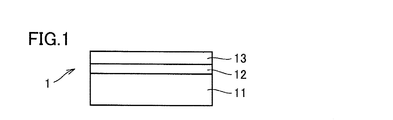
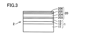
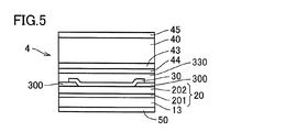
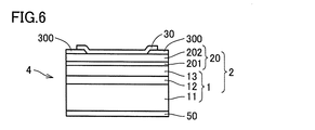
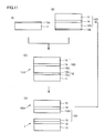
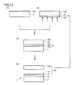
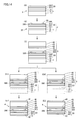
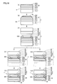
- FIG. 1 It is a schematic sectional drawing which shows a certain example of the manufacturing method of the group III nitride composite substrate using an ion implantation method. It is a schematic sectional drawing which shows a certain example of the manufacturing method of the group III nitride semiconductor device concerning this invention. It is a schematic sectional drawing which shows another example of the manufacturing method of the group III nitride semiconductor device concerning this invention. It is a schematic sectional drawing which shows another example of the manufacturing method of the group III nitride semiconductor device concerning this invention. It is a schematic sectional drawing which shows another example of the manufacturing method of the group III nitride semiconductor device concerning this invention. FIG.
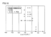
- Difference in thermal expansion coefficient and Young's modulus ratio between the support substrate of the group III nitride substrate and the group III nitride film, and the thickness ratio between the support substrate of the group III nitride substrate and the group III nitride film 4 is a graph showing the relationship between the uniformity of the in-plane distribution of the carrier concentration of the group III nitride layer.
- a group III nitride composite substrate 1 includes a support substrate 11 having a thickness t S of 0.1 mm or more and 1 mm or less, and a thickness t f that is smaller than the thickness t s of 0.01 mm.
- the group III nitride composite substrate 1 having a diameter of 75 mm or more is bonded to the group III nitride film 13 of 0.25 mm or less.
- the group III nitride composite substrate 1 of this embodiment has an absolute value
- of the thermal expansion coefficient difference ⁇ between the support substrate 11 and the group III nitride film 13 is 2.2 ⁇ 10 ⁇ 6 K ⁇ 1 or less.
- the Young's modulus E s and thickness t s of the support substrate 11, the Young's modulus E f and thickness t f of the group III nitride film 13, and the thermal expansion coefficient difference ⁇ are expressed by the above formula (1). Therefore, at least one group III nitride layer 20 having a large diameter and high crystal quality is grown on the group III nitride film 13, and the group III nitride semiconductor device 4 having high characteristics is obtained with high yield. Can be produced.
- the laminated group III nitride composite substrate 2 which is another embodiment of the present invention is disposed on the group III nitride composite substrate 1 of the above embodiment and the group III nitride film 13 of the group III nitride composite substrate 1. And at least one III-nitride layer 20.
- the group III nitride layer 20 disposed on the group III nitride film 13 also has a high crystal quality. Can be manufactured with high yield.
- a group III nitride semiconductor device 4 which is still another embodiment of the present invention includes at least one group III nitride layer 20 in the laminated group III nitride composite substrate 2 of the above embodiment.
- the group III nitride semiconductor device 4 of the present embodiment includes the group III nitride layer 20 with high crystal quality, and thus has high characteristics.
- a group III nitride semiconductor device 4 which is still another embodiment of the present invention is disposed on the group III nitride film 13 and the group III nitride film 13 in the group III nitride composite substrate 1 of the above embodiment. And at least one group III nitride layer 20.
- the group III nitride semiconductor device 4 of the present embodiment includes the group III nitride layer 20 having a high crystal quality disposed on the group III nitride film 13, and thus has high characteristics.
- the group III nitride semiconductor device 4 according to the embodiment of the present invention can further include at least one of the support substrate 11 and the device support substrate 40. Thereby, the mechanical strength of the group III nitride semiconductor device 4 is maintained high.
- a method for manufacturing a group III nitride composite substrate 1 according to still another embodiment of the present invention is a method for manufacturing a group III nitride composite substrate 1 according to the above embodiment, including a support substrate 11 and a group III nitride film. Bonding the donor substrate 13D to the bonding substrate 1L, 1LS having a diameter of 75 mm or more, and a predetermined inside from the bonding main surface of the group III nitride film donor substrate 13D of the bonding substrate 1L, 1LS. Forming the group III nitride composite substrate 1 by cutting the group III nitride film donor substrate 13D at a plane located at a distance of.
- the manufacturing method of the group III nitride composite substrate 1 of this embodiment efficiently manufactures the large-diameter group III nitride composite substrate 1 having the group III nitride film 13 having a large film thickness and high crystal quality at low cost. be able to.
- a method for manufacturing a group III nitride composite substrate 1 according to still another embodiment of the present invention is a method for manufacturing a group III nitride composite substrate 1 according to the above embodiment, including a support substrate 11 and a group III nitride film.
- the bonding substrate 1L is bonded to the donor substrate 13D to form a bonding substrate 1L having a diameter of 75 mm or more, and the bonding substrate 1L is ground from the main surface opposite to the bonding main surface of the group III nitride film donor substrate 13D.
- a step of forming group III nitride composite substrate 1 by performing at least one of polishing and etching.
- the manufacturing method of the group III nitride composite substrate 1 of this embodiment efficiently manufactures the large-diameter group III nitride composite substrate 1 having the group III nitride film 13 having a large film thickness and high crystal quality at low cost. be able to.
- a method for manufacturing a group III nitride semiconductor device 4 according to still another embodiment of the present invention includes a step of preparing the group III nitride composite substrate 1 of the above embodiment, and a group III nitride of the group III nitride composite substrate 1. Growing at least one group III nitride layer 20 on the material film 13.
- the manufacturing method of the group III nitride semiconductor device 4 of this embodiment can manufacture the group III nitride semiconductor device 4 having high characteristics with a high yield.
- the device supporting substrate 40 is further bonded to the group III nitride layer 20, and the supporting substrate 11 is bonded from the group III nitride composite substrate 1. And a removing step.
- the group III nitride semiconductor device 4 having high mechanical strength and high characteristics supported by the device support substrate 40 can be manufactured with high yield.
- III-nitride composite substrate 1 which is an embodiment of the present invention, the following supporting substrate 11 thickness t s is 0.1mm or 1 mm, thinner than the thickness t s
- the group III nitride composite substrate 1 having a diameter of 75 mm or more is bonded to the group III nitride film 13 having a thickness t f of 0.01 mm to 0.25 mm.
- the coefficient of thermal expansion ⁇ s (unit: x) of the support substrate 11 is calculated from the coefficient of thermal expansion ⁇ f (unit: x 10 ⁇ 6 K ⁇ 1 ) of the group III nitride film 13.
- of the thermal expansion coefficient difference ⁇ minus 10 ⁇ 6 K ⁇ 1 ) is 2.2 ⁇ 10 ⁇ 6 K ⁇ 1 or less
- the Young's modulus E s (unit: GPa) of the support substrate 11 and Thickness t s (unit: mm), Young's modulus E f (unit: GPa) and thickness t f (unit: mm) of group III nitride film 13, and thermal expansion coefficient difference ⁇ (unit: ⁇ 10 ⁇ 6) K -1) is the following formula (1) t s 2 / t f ⁇ 6E f ⁇
- of the thermal expansion coefficient difference ⁇ between the support substrate 11 and the group III nitride film 13 is 2.2 ⁇ 10 ⁇ 6 K ⁇ 1 or less.
- the Young's modulus E s and thickness t s of the support substrate 11, the Young's modulus E f and thickness t f of the group III nitride film 13, and the thermal expansion coefficient difference ⁇ are expressed by the above formula (1
- at least one group III nitride layer 20 having a large diameter and high crystal quality is grown on the group III nitride film 13 to obtain a group III nitride semiconductor device 4 having high characteristics. Can be made well.
- the form of the group III nitride composite substrate 1 of the present embodiment is not particularly limited, and even if the support substrate 11 and the group III nitride film 13 are directly bonded together, the support substrate 11 and the group III The nitride film 13 may be indirectly bonded with the bonding film 12 interposed therebetween. From the viewpoint of increasing the bonding strength by bonding, a mode in which the support substrate 11 and the group III nitride film 13 are bonded indirectly with the bonding film 12 interposed therebetween is preferable.
- the diameter of the group III nitride composite substrate 1 of the present embodiment is 75 mm or more, preferably 100 mm or more, more preferably 125 mm or more from the viewpoint of increasing the number of chips of a semiconductor device from one composite substrate.
- 150 mm or more is more preferable.
- the diameter of the group III nitride composite substrate 1 is preferably 300 mm or less, and more preferably 200 mm or less, from the viewpoint of reducing the warpage of the composite substrate and increasing the yield of the semiconductor device.
- the thickness t f of the group III nitride film 13 is set to 0.01 mm from the viewpoint of forming a group III nitride semiconductor device having high characteristics with a high yield by growing a group III nitride layer having a high crystal quality thereon. It is above, 0.02 mm or more is preferable and 0.05 mm or more is more preferable. Further, from the viewpoint of reducing the cost by reducing the amount of expensive group III nitride used, it is 0.25 mm or less, preferably 0.15 mm or less, and more preferably 0.1 mm or less.
- of the thermal expansion coefficient difference ⁇ obtained by subtracting the thermal expansion coefficient ⁇ s of the support substrate 11 from the thermal expansion coefficient ⁇ f of the group III nitride film 13 is a group III without causing cracks and / or peeling. From the viewpoint of forming a group III nitride semiconductor device having high characteristics with high yield by growing a group III nitride layer having high crystal quality on the nitride film 13, it is 2.2 ⁇ 10 ⁇ 6 K ⁇ 1 or less. 2.0 ⁇ 10 ⁇ 6 K ⁇ 1 or less is preferable, and 1.5 ⁇ 10 ⁇ 6 K ⁇ 1 or less is more preferable.
- the group III nitride bonded to the support substrate 11 of the group III nitride composite substrate 1 is grown.
- the thermal stress ⁇ T (unit: Pa) applied to the film 13 varies from the thermal expansion coefficient ⁇ f (unit: ⁇ 10 ⁇ 6 K ⁇ 1 ) of the group III nitride film 13 to the thermal expansion coefficient ⁇ S (unit) of the support substrate 11.
- a curvature radius R (unit: m) due to the warp of the group III nitride composite substrate 1 when growing at least one group III nitride layer on the group III nitride film 13 of the group III nitride composite substrate 1.
- E s unit: GPa
- t s unit: mm
- t f unit: mm
- T thermal stress
- This equation (5) is for E f ⁇
- III is grown on the group III nitride film 13 of the group III nitride composite substrate 1.
- Young's modulus E s and thickness t s of support substrate 11, Young of group III nitride film 13 were evaluated.
- Supporting substrate 11 has a thickness t S is not more 0.1mm to 1mm, and is not particularly limited as long as it satisfies the relationship of formula (1), of expensive Group III nitride From the viewpoint of reducing the usage amount and reducing the cost, it is preferable that the substrate is a different composition substrate having a different group III nitride chemical composition. From the above viewpoint, the support substrate 11 is made of, for example, an oxide substrate made of an oxide such as mullite, zirconia, mullite-YSZ (yttria stabilized zirconia), sapphire, alumina, or silicon (Si).
- oxide substrate made of an oxide such as mullite, zirconia, mullite-YSZ (yttria stabilized zirconia), sapphire, alumina, or silicon (Si).
- a silicon substrate, a silicon carbide substrate formed of silicon carbide (SiC), a metal substrate formed of molybdenum (Mo), tungsten (W), copper tungsten (CuW), or the like is preferable.
- the support substrate 11 is preferably a conductive support substrate from the viewpoint of manufacturing a vertical device including the group III nitride composite substrate 1, and is preferably a metal substrate such as a Mo substrate or a W substrate.
- the group III nitride film 13 is not particularly limited as long as the thickness t f is 0.01 mm or more and 0.25 mm or less and satisfies the relationship of the above formula (1).
- a dopant for adjusting the carrier concentration may be added.
- the bonding film 12 is not particularly limited as long as it can bond the support substrate 11 and the group III nitride film 13, but from the viewpoint of high bondability between the support substrate 11 and the group III nitride film 13, silicon oxide.
- a (SiO 2 ) film, a silicon nitride (SiN x ) film, a titanium oxide (TiO 2 ) film, a gallium oxide (Ga 2 O 3 ) film, or the like is preferable.
- the bonding film 12 is preferably a conductive bonding film from the viewpoint of manufacturing a vertical device including the group III nitride composite substrate 1, for example, a TiO 2 film, a Ga 2 O 3 film, or the like.
- a laminated group III nitride composite substrate 2 which is another embodiment of the present invention includes a group III nitride composite substrate 1 of embodiment 1 and a group III nitride composite substrate 1. And at least one group III nitride layer 20 disposed on the group III nitride film 13.
- the group III nitride layer 20 disposed on the group III nitride film 13 also has a high crystal quality. It can be manufactured with good yield.
- group III nitride layer 20 in the laminated group III nitride composite substrate 2 of the present embodiment, the configuration of the group III nitride layer 20 disposed on the group III nitride film 13 differs depending on the type of group III nitride semiconductor device to be manufactured. .
- group III nitride layer 20 when fabricating an SBD (Schottky barrier diode) as an example of an electronic device as a group III nitride semiconductor device, group III nitride layer 20 includes, for example, n + -GaN layer 201. (Carrier concentration is, for example, 2 ⁇ 10 18 cm ⁇ 3 ) and n ⁇ -GaN layer 202 (carrier concentration is, for example, 1 ⁇ 10 16 cm ⁇ 3 ).
- group III nitride layer 20 when fabricating a PND (pn junction diode) which is another example of an electronic device as a group III nitride semiconductor device, group III nitride layer 20 includes, for example, n + -GaN layer 203.
- Carrier concentration is 2 ⁇ 10 18 cm ⁇ 3
- n ⁇ -GaN layer 204 carrier concentration is 1 ⁇ 10 16 cm ⁇ 3
- p ⁇ —GaN layer 205 Mg concentration is 5 ⁇ 10 17 cm, for example) -3
- a p + -GaN layer 206 Mg concentration is, for example, 1 ⁇ 10 20 cm -3 ).
- a group III nitride semiconductor device 4 which is still another embodiment of the present invention includes at least a group III nitride layer 20 in the laminated group III nitride composite substrate 2 of the second embodiment. including. That is, the group III nitride semiconductor device 4 of the present embodiment includes at least a group III nitride layer 20 as the first type.
- the group III nitride semiconductor device 4 of the present embodiment includes the group III nitride layer 20 with high crystal quality, and thus has high characteristics.
- the group III nitride semiconductor device 4 that is still another embodiment of the present invention is the group III nitride composite substrate of the first embodiment. 1 group III nitride film 13 and at least one group III nitride layer 20 disposed on group III nitride film 13. That is, the group III nitride semiconductor device 4 of the present embodiment includes at least the group III nitride film 13 in addition to the group III nitride layer 20 included in the first type as the second type.
- the group III nitride semiconductor device 4 of the present embodiment includes the group III nitride layer 20 having a high crystal quality disposed on the group III nitride film 13, and thus has high characteristics.
- the group III nitride semiconductor device 4 of the above embodiment is a group III nitride layer 20 included in the first type or the second type.
- the group III nitride semiconductor device 4 further includes at least one of the support substrate 11 and the device support substrate 40, so that the mechanical strength is maintained high.
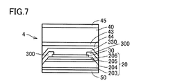
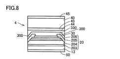
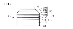
- the group III nitride semiconductor device 4 further including at least one of the support substrate 11 and the device support substrate 40 includes a third type further including the support substrate 11 shown in FIGS. 6 and 9, and FIGS. 5, and a fourth type further including a device support substrate 40 shown in FIGS.
- group III nitride semiconductor device 4 which is an SBD (Schottky barrier diode) includes, for example, an n + -GaN layer 201 (with a carrier concentration of 2 ⁇ 10 2, for example) as a first type. 18 cm ⁇ 3 ) and the n ⁇ -GaN layer 202 (carrier concentration is, for example, 1 ⁇ 10 16 cm ⁇ 3 ), and the group III nitride layer 20 on the n ⁇ -GaN layer 202 side.
- the first electrode 30 that is a Schottky electrode to be disposed and the second electrode 50 that is an ohmic electrode disposed on the n + -GaN layer 201 side of the group III nitride layer 20 can be included.
- group III nitride semiconductor device 4 which is a PND (pn junction diode) includes, for example, an n + -GaN layer 203 (with a carrier concentration of 2 ⁇ , for example) as a first type.
- n ⁇ -GaN layer 204 carrier concentration is, for example, 1 ⁇ 10 16 cm ⁇ 3
- p ⁇ —GaN layer 205 Mg concentration is, for example, 5 ⁇ 10 17 cm ⁇ 3
- p + A group III nitride layer 20 including a -GaN layer 206 Mg concentration is, for example, 1 ⁇ 10 20 cm -3
- positioned at the n ⁇ +>- GaN layer 203 side of the group III nitride layer 20 can be included.
- a second type III-nitride including a group III nitride film 13 in addition to the first type III-nitride semiconductor device 4 described above.
- the group III nitride film 13 is disposed on the second electrode 50 side of the group III nitride layer 20, for example.
- a third type III-nitride semiconductor device 4 further including a supporting substrate 11 in the first type or second type III-nitride semiconductor device 4 described above.
- the support substrate 11 is disposed between the group III nitride layer 20 and the second electrode 50, for example.
- the support substrate 11 is derived from the support substrate 11 of the group III nitride composite substrate 1 of the first embodiment.
- a fourth type III that further includes a device support substrate 40 in the first type or second type III-nitride semiconductor device 4.
- the device support substrate 40 is disposed, for example, on the first electrode 30 side of the group III nitride layer 20.
- the device support substrate 40 is preferably a metal substrate such as a Mo substrate, a W substrate, or a CuW substrate, a Si substrate, or the like from the viewpoint of supporting the group III nitride layer 20 and having conductivity.
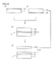
- the manufacturing method of the group III nitride composite substrate 1 which is further another embodiment of this invention is a manufacturing method of the group III nitride composite substrate 1 of Embodiment 1, A step of forming bonded substrates 1L and 1LS having a diameter of 75 mm or more by bonding the support substrate 11 and the group III nitride film donor substrate 13D (FIGS. 10A to 10C, FIG.
- the manufacturing method of the group III nitride composite substrate 1 of this embodiment efficiently manufactures the large-diameter group III nitride composite substrate 1 having the group III nitride film 13 having a large film thickness and high crystal quality at low cost. be able to.
- the group III nitride film donor substrate 13D is positioned at a predetermined distance from the bonding main surface of the group III nitride film donor substrate 13D when cutting the group III nitride film donor substrate 13D.
- the predetermined distance on the surface to be processed is determined according to the thickness of the group III nitride film 13 of the group III nitride composite substrate 1 to be manufactured.
- the bonded main surface of the group III nitride film 13 and The thickness of group III nitride film 13 can be reduced by performing at least one of grinding, polishing, and etching from the opposite main surface.
- the group III nitride composite substrate 1 obtained by cutting is used.
- the main surface of group III nitride film 13 is preferably polished.
- the polishing method is preferably precision polishing by CMP (chemical mechanical polishing), chemical polishing, or the like.
- the predetermined distance on the surface located at a predetermined distance from the main bonding surface of the group III nitride film donor substrate 13D when the group III nitride film donor substrate 13D is cut is the object of manufacture. It is preferable to set the distance obtained by adding the thickness of the group III nitride film 13 of the group III nitride composite substrate 1 to the thickness of the polishing allowance.
- the group III nitride is a surface located at a predetermined distance from the bonded main surface of the group III nitride film donor substrate 13D of the bonding substrates 1L and 1LS.
- the group III nitride film 13 is formed by cutting the film donor substrate 13D, and preferably at least one of grinding, polishing, and etching is performed from the main surface opposite to the bonding main surface of the group III nitride film 13.
- the group III nitride composite substrate 1 including the group III nitride film 13 having a desired thickness of 0.01 mm or more and 0.25 mm or less is obtained by adjusting the film thickness to be reduced.
- the thickness of the group III nitride film donor substrate 13D used is preferably greater than 0.5 mm, more preferably 1 mm or more, and even more preferably 2 mm or more.
- the step of forming the bonding substrates 1L and 1LS is a sub-process for forming the bonding film 12a on the main surface of the support substrate 11.
- Step (FIGS. 10A and 11A) and a sub-step of forming the bonding film 12b on the main surface of the group III nitride film donor substrate 13D (FIGS. 10B and 11B)
- a sub-step of bonding the bonding film 12a formed on the support substrate 11 and the bonding film 12b formed on the group III nitride film donor substrate 13D (FIGS. 10C and 11C).
- bonding film 12a is integrated with bonding film 12b described later to form a bonding film.
- 12 is formed of the same material as that of the bonding film 12.
- the method for forming the bonding film 12a is not particularly limited as long as it is suitable for the formation of the bonding film 12a.
- sputtering, CVD (chemical vapor) Phase deposition) method, PLD (pulse laser deposition) method, MBE (molecular beam growth) method, electron beam evaporation method and the like are preferable.
- CVD is particularly preferable because it increases the quality of the bonding film and increases the deposition rate.
- the P-CVD plasma-chemical vapor deposition
- LP- from the viewpoint of improving the film quality and facilitating mass production.
- a CVD (reduced pressure-chemical vapor deposition) method or the like is more preferable.
- annealing can be performed after the bonding films 12a and 12b are formed and before bonding. By this annealing, the bonding films 12a and 12b can be degassed to densify the bonding films 12a and 12b.
- the bonding film 12a has a mirror surface (for example, an RMS (root mean square roughness) of 0.3 nm or less) from the viewpoint of increasing the bonding strength between the support substrate 11 and the group III nitride film donor substrate 13D. It is preferable to polish the mirror surface.
- the method for polishing the main surface of the bonding film 12a is not particularly limited, and for example, CMP (Chemical Mechanical Polishing) is used. From the viewpoint of increasing the bonding strength, in order to improve the cleanliness of the bonding film, non-abrasive polishing with a liquid that does not contain abrasive grains can be performed after CMP.
- non-abrasive polishing with an alkali such as KOH or TMAH (tetramethylammonium hydroxide), or an acid such as HCl, HNO 3 , or H 2 SO 4 can be performed.
- an alkali such as KOH or TMAH (tetramethylammonium hydroxide), or an acid such as HCl, HNO 3 , or H 2 SO 4
- scrub cleaning using a sponge, a brush, or the like can be performed in order to improve the cleanliness of the bonding film.
- Two-fluid cleaning, megasonic cleaning, ultrasonic cleaning, and the like can also be suitably performed.
- group III nitride film donor substrate 13D is This is a donor substrate that provides a group III nitride film 13 by separation in a sub-process.
- the method for preparing such a group III nitride film donor substrate 13D is not particularly limited, but from the viewpoint of obtaining a group III nitride film donor substrate 13D having good crystallinity, the HVPE (hydride vapor phase epitaxy) method, MOVPE (organic)
- a vapor phase method such as a metal vapor phase growth method, an MBE (molecular beam growth) method, a sublimation method, a liquid phase method such as a flux method, a high nitrogen pressure solution method, and an ammonothermal method is preferable.
- the material and method for forming the bonding film 12b and the polishing of the main surface are the same as the material and method for forming the bonding film 12a and the polishing of the main surface, respectively.
- the bonding method is not particularly limited, and the bonding surface is cleaned and bonded as it is, then the direct bonding method in which the temperature is raised to about 600 ° C. to 1200 ° C. and the bonding surface is cleaned, and plasma or ions are used for cleaning.
- Surface activated bonding method in which bonding is performed in a low temperature atmosphere of about room temperature (for example, 25 ° C.) to about 400 ° C.
- the bonding strength can be further increased by raising the temperature to about 600 ° C. to 1200 ° C. after the bonding.
- the effect of increasing the bonding strength by raising the temperature to about 600 ° C. to 1200 ° C. after the bonding is large.
- the bonding film 12a and the bonding film 12b are integrated by bonding to form the bonding film 12, and the support substrate 11 and the group III nitride film donor substrate 13D are bonded with the bonding film 12 interposed therebetween.
- the bonded substrates 1L and 1LS are formed.
- the bonding strength can be increased by activating the bonding surfaces of the bonding films 12a and 12b before bonding.
- the activation of the bonding surface is not particularly limited, but is preferably performed by plasma treatment, ion treatment, chemical treatment with a chemical solution, cleaning treatment, CMP treatment or the like from the viewpoint of high activation effect.
- Group III nitride composite substrate formation process Referring to FIGS. 10D and 11D, in the step of forming group III nitride composite substrate 1, from the bonded main surface of group III nitride film donor substrate 13D of bonding substrates 1L and 1LS to the inside
- the group III nitride film 13 bonded to the support substrate 11 with the bonding film 12 interposed therebetween is cut by cutting the group III nitride film donor substrate 13D at a surface located at a predetermined distance, and the remaining group III nitride Separated into film donor substrate 13Dr, group III nitride composite substrate 1 is formed in which support substrate 11 and group III nitride film 13 are bonded together with bonding film 12 interposed.
- the method for cutting the group III nitride film donor substrate 13D is not particularly limited, and examples thereof include a wire saw, a blade saw, laser processing, electric discharge processing, and water jet.
- the group III nitride film donor substrate 13D is cut with a wire saw
- the loose abrasive method is preferred.
- the wire tension is increased in order to reduce the bending of the wire due to the cutting resistance and increase the accuracy and flatness of the thickness. It is preferable to increase the speed.
- a highly rigid wire saw device is preferable.
- the wire is oscillated and the group III nitride film donor substrate 13D is oscillated in synchronization therewith.
- the group III nitride film donor substrate 13D moves in the cutting progress direction.
- the group III nitride film donor substrate 13D moves in a direction opposite to the cutting progress direction when the wire saw is positioned at an angle far from the perpendicular to the cutting progress direction of the group III nitride film donor substrate 13D.
- group III nitrides such as GaN are more brittle and easier to break than sapphire and SiC, and therefore cannot be cut well by the same cutting method as sapphire and SiC.
- the viscosity ⁇ (Pa ⁇ s) of the machining fluid for slicing, the flow rate Q (m 3 / s) of the machining fluid, and the wire linear velocity V (m / S), maximum cutting length L (m), cutting speed P (m / s), and simultaneous cutting number n expressed as ( ⁇ ⁇ Q ⁇ V) / (L ⁇ P ⁇ n).
- the resistance coefficient RC (N) is in an appropriate range, specifically 4000 or more and 5000 or less.
- the manufacturing method of the group III nitride composite substrate of the present embodiment from the viewpoint of removing the damaged layer of the group III nitride film 13 formed by cutting, maintaining high crystal quality, and smoothing the main surface, It is preferable to polish the main surface of the group III nitride film 13 of the group III nitride composite substrate 1 obtained by cutting.
- the bonding main group III group nitride film donor substrate 13D which is a surface for cutting the group III nitride film donor substrate 13D of the bonding substrates 1L and 1LS is mainly bonded.
- the predetermined distance on the surface located at a predetermined distance from the surface is the thickness of the group III nitride film 13 of the group III nitride composite substrate 1 to be manufactured and the thickness of the polishing allowance. It is preferable that the distance is added.
- the polishing allowance is not particularly limited, but is preferably 0.01 mm or more, more preferably 0.02 mm or more, and further preferably 0.03 mm or more from the viewpoint of removing the damaged layer.
- the polishing allowance is preferably 0.1 mm or less, more preferably 0.08 mm or less, and further preferably 0.06 mm or less, from the viewpoint of reducing material loss of the group III nitride film donor substrate 13D.
- the remaining group III nitride film donor substrate 13Dr is repeatedly used by polishing its main surface. Can do.
- a group-provided group III nitride film donor substrate 16D in which a group III nitride film donor substrate support 15 is bonded to a group III nitride film donor substrate 13D is used.
- the group III nitride composite substrate 1 can be manufactured in the same manner as described above.
- the group III nitride film donor substrate 16D with support the group III nitride film donor substrate 13D is supported by the group III nitride film donor substrate support 15, and therefore the group III nitride film donor substrate 13D cannot stand alone. Even if it becomes as thin as possible, it can be used repeatedly.
- the bonding form of the group III nitride film donor substrate support 15 and the group III nitride film donor substrate 13D is not particularly limited, but the bonding strength by bonding is not limited. In order to increase the thickness, it is preferable to interpose the bonding film 14.
- the group III nitride film donor substrate support 15 is not particularly limited, but is formed of a material having the same physical properties as the support substrate 11 from the viewpoint of high support strength and prevention of cracks and warpage. It is preferable.
- the bonding film 14 is not particularly limited, but from the viewpoint of high bondability between the group III nitride film donor substrate support 15 and the group III nitride film donor substrate 13D, the SiO 2 film, the SiN x film, and the TiO 2 film.
- a Ga 2 O 3 film or the like is preferable.
- the method for manufacturing group III nitride composite substrate 1 is the method for manufacturing group III nitride composite substrate 1 of embodiment 1, and includes support substrate 11. Are bonded to the group III nitride film donor substrate 13D to form a bonded substrate 1L having a diameter of 75 mm or more (FIGS. 12A to 12C), and the group III nitride of the bonded substrate 1L.
- the group III nitride composite substrate 1 having a group III nitride film having a low cost, a large diameter, a large film thickness and a high crystal quality is efficiently manufactured. can do.
- the group III nitride composite substrate 1 including the group III nitride film 13 having a desired thickness of 0.01 mm or more and 0.25 mm or less is obtained by adjusting the film thickness to be reduced.
- the manufacturing method of the group III nitride composite substrate 1 of this embodiment it grinds from the main surface on the opposite side to the bonding main surface of the group III nitride film donor substrate in the step of forming the group III nitride composite substrate.
- the thickness of the group III nitride film donor substrate 13D used is preferably 0.5 mm or less. 0.4 mm or less is more preferable.
- the step of forming the bonding substrate 1L is performed on the main surface of the support substrate 11 in the same manner as the method for manufacturing the group III nitride composite substrate 1 of the embodiment 4-1.
- a sub-process for forming the bonding film 12a (FIG. 12A), a sub-process for forming the bonding film 12b on the main surface of the group III nitride film donor substrate 13D (FIG. 12B), and a supporting substrate.
- the sub-process for forming the bonding film 12a on the main surface of the support substrate 11 shown in FIG. 12A is a sub-process for forming the bonding film 12a on the main surface of the support substrate 11 shown in FIG. It is the same as the process.
- the sub-process for forming the bonding film 12b on the main surface of the group III nitride film donor substrate 13D shown in FIG. 12B is performed on the main surface of the group III nitride film donor substrate 13D shown in FIG. This is the same as the sub-process for forming the bonding film 12b.
- Group III nitride composite substrate formation process Referring to FIG. 12D, in the step of forming group III nitride composite substrate 1, grinding and polishing are performed from the main surface opposite to the bonded main surface of group III nitride film donor substrate 13D of bonding substrate 1L. By performing at least one of etching and etching, the group III nitride film 13 having a reduced thickness is formed from the group III nitride film donor substrate 13D, and the support substrate 11 and the group III nitride film 13 are bonded to each other. Group III nitride composite substrate 1 bonded with film 12 interposed therebetween is formed.
- the method for grinding the group III nitride film donor substrate 13D is not particularly limited, and examples thereof include grinding using a grindstone or abrasive grains.
- the method for polishing the group III nitride film donor substrate 13D is not particularly limited, and examples thereof include rough polishing such as mechanical polishing, precision polishing such as CMP, and chemical polishing.
- the method for etching the group III nitride film donor substrate 13D is not particularly limited, and examples include wet etching using a chemical solution and dry etching such as RIE (reactive ion etching).
- the group III nitride composite substrate obtained by at least one of grinding and etching It is preferable to polish the main surface of one group III nitride film 13.
- the thickness reduction amount due to at least one of grinding, polishing, and etching is preferably 0.01 mm or more, more preferably 0.02 mm or more, and further preferably 0.03 mm or more.
- the amount of decrease in thickness due to at least one of grinding, polishing, and etching is preferably 0.1 mm or less, more preferably 0.08 mm or less, from the viewpoint of reducing the material loss of the group III nitride film donor substrate 13D. 0.06 mm or less is more preferable.
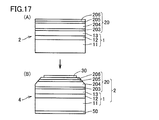
- the manufacturing method of group III nitride semiconductor device 4 which is still another embodiment of the present invention includes the step of preparing group III nitride composite substrate 1 of embodiment 1, and III Step of growing at least one group III nitride layer 20 on group III nitride film 13 of group nitride composite substrate 1 (FIG. 14A, FIG. 15A, FIG. 16A and FIG. 17 (A)).
- a high-performance group III nitride semiconductor device can be manufactured with high yield.
- the step of further bonding the device support substrate 40 on the group III nitride layer 20 (FIGS. 14C and 16C), and the group III
- the step of removing the support substrate 11 from the nitride composite substrate 1 (FIG. 14 (D1) or (D2) and FIG. 16 (D1) or (D2)) may further be included.
- a group III nitride semiconductor device having high mechanical strength and high characteristics supported by the device support substrate 40 can be manufactured with high yield.
- the method for manufacturing the group III nitride semiconductor device 4 of the present embodiment can be performed by the following steps.
- the method of growing the group III nitride layer 20 includes the MOVPE method, the MBE method, the HVPE method, and the sublimation method from the viewpoint of epitaxially growing the group III nitride layer 20 with high crystal quality.
- a vapor phase method such as a liquid phase method such as a flux method is preferable, and a MOVPE method is particularly preferable.
- group III nitride layer 20 differs depending on the type of group III nitride semiconductor device 4. Referring to FIGS. 14 and 15, when group III nitride semiconductor device 4 is an SBD (Schottky barrier diode), group III nitride layer 20 is formed, for example, on group III nitride film 13 with n + A ⁇ GaN layer 201 (with a carrier concentration of, for example, 2 ⁇ 10 18 cm ⁇ 3 ) and an n ⁇ —GaN layer 202 (with a carrier concentration of, for example, 1 ⁇ 10 16 cm ⁇ 3 ) can be grown in order.
- SBD Schottky barrier diode
- group II nitride layer 20 is formed on group III nitride film 13, for example, n + ⁇ GaN layer 203 (carrier concentration is, for example, 2 ⁇ 10 18 cm ⁇ 3 ), n ⁇ —GaN layer 204 (carrier concentration is, for example, 1 ⁇ 10 16 cm ⁇ 3 ), p ⁇ —GaN layer 205 (Mg concentration is, for example, 5 ⁇ 10 17 cm ⁇ 3 ) and p + -GaN layer 206 (Mg concentration is, for example, 1 ⁇ 10 20 cm ⁇ 3 ).
- the laminated group III nitride composite substrate 2 is obtained by growing at least one group III nitride layer 20 on the group III nitride film 13 of the group III nitride composite substrate 1. .
- the group III nitride semiconductor device of this embodiment is used from the viewpoint of efficient manufacturing.
- 4 includes the steps of growing at least one group III nitride layer 20 on the group III nitride film 13 of the group III nitride composite substrate 1 and manufacturing the following electrodes: It is preferable to include.
- the group III nitride semiconductor device 4 including the support substrate 11 is manufactured, the device support substrate is not required, and therefore the step of bonding the device support substrate 40 as shown in FIGS. 14 and 16 is not included. Also good.
- Electrode formation process Referring to FIG. 15B, when an SBD is manufactured as group III nitride semiconductor device 4, for example, insulating film 300 having an opening on the n ⁇ -GaN layer 202 side of group III nitride layer 20. Then, a Schottky electrode is formed as the first electrode 30, and an ohmic electrode is formed as the second electrode 50 on the support substrate 11 on the n + -GaN layer 202 side of the group III nitride layer 20. Referring to FIG.
- a mesa portion is formed in a part of the group III nitride layer 20, and the group III nitride layer is formed.
- An ohmic electrode is formed as the first electrode 30 on the p + -GaN layer 206 side of 20 and an ohmic electrode is formed as the second electrode 50 on the support substrate 11 on the n + -GaN layer 203 side of the group III nitride layer 20.
- the method for forming these electrodes is not particularly limited as long as it is suitable for the material of the electrode to be formed, and a vacuum deposition method, a sputtering method, or the like is used.
- the step of further bonding the device support substrate 40 on the group III nitride layer 20 is performed by stacking the group III An insulating film 300 having an opening is formed on group III nitride layer 20 of nitride composite substrate 2, and a first electrode is formed on part of insulating film 300 and group III nitride layer 20 in the opening of insulating film 300.
- the insulating film 300 in which the first electrode 30 of the laminated group III nitride composite substrate 2E with electrode is not formed The barrier film 330 is formed on the first electrode 30, the pad electrode 43 and the bonding metal film 44 are formed on the device support substrate 40, and the bonding metal is formed on the barrier film 330. Carried out by attaching the 44.
- the step of further bonding the device support substrate 40 on the group III nitride layer 20 includes the group III nitridation.
- the mesa portion is formed in a part of the physical layer 20 and the first electrode 30 is formed on the group III nitride layer 20 to form the laminated group III nitride composite substrate 2E with electrode.
- Insulating film 300 is formed on part of first electrode 30 of group nitride composite substrate 2E and the leg surface of the mesa portion of group III nitride layer 20, and barrier film 330 is formed on first electrode 30 and insulating film 300.
- the pad electrode 43 and the bonding metal film 44 are formed on the device support substrate 40, and the bonding metal film 44 is bonded to the barrier film 330.
- the laminated substrate 3 is obtained by the step of bonding the device support substrate 40 described above.
- FIG. 14D1 and FIG. 16D1 in the step of removing support substrate 11 from group III nitride composite substrate 1, support substrate 11 of group III nitride composite substrate 1 is removed from laminated substrate 3. This is done by removing.
- the bonding film 12 in the group III nitride composite substrate 1, when the bonding film 12 is interposed between the support substrate 11 and the group III nitride film 13, the bonding film 12 can also be removed.
- FIGS. 14D2 and 16D2 in addition to supporting substrate 11 and bonding film 12, group III nitride film 13 can also be removed.
- the group III nitride film 13 of the group III nitride composite substrate 1 is damaged, the group III nitride semiconductor device 4 having high characteristics is removed by removing the damaged group III nitride film 13. Is obtained.
- the method for removing the support substrate 11, the bonding film 12, and / or the group III nitride film 13 is not particularly limited, and grinding, polishing, etching, and the like are preferably used.
- the support substrate 11 formed of a material that has low hardness, strength, and wear resistance and is easily cut can be removed by at least one of grinding and polishing from the viewpoint of reducing manufacturing costs.
- the support substrate 11 formed of a material that dissolves in a chemical solution such as acid or alkali can be removed by etching with a chemical solution from the viewpoint of low manufacturing cost.
- the support substrate 11 has a larger number of ceramics or the like than a support substrate formed of a single crystal material such as sapphire, SiC, or a group III nitride (for example, GaN).
- a support substrate made of a crystalline material is preferred.
- a second electrode 50 is formed on group III nitride film 13 exposed by removing support substrate 11 and bonding film 12 from laminated substrate 3.
- the device support substrate electrode 45 is formed on the device support substrate 40.
- group III nitride layer 20 exposed by removing support substrate 11, bonding film 12, and group III nitride film 13 from laminated substrate 3 is used.
- the second electrode 50 is formed thereon, and the device support substrate electrode 45 is formed on the device support substrate 40.
- Example A 1. Preparation of Group III Nitride Composite Substrate With reference to FIG. 10A, a support substrate 11 having a diameter of 75 mm and a thickness of 0.5 mm formed from the materials shown in each of Examples A1 to A12 in Table 1 was prepared. .
- the material of the support substrate 11 in each example is mullite in which Example A1 is 60 mol% Al 2 O 3 and 40 mol% SiO 2 with respect to the entire substrate, Example A2 is sapphire, and Example A3 is alumina.
- example A4 is SiO 2 glass
- example A5 is Al 2 O 3 is Al 2 O 3 -SiO 2 composite oxide of SiO 2 is 15 mass% at 85 wt% with respect to the entire substrate
- example A6 Is 70% by weight of mullite and 30% by weight of YSZ (yttria-stabilized zirconia), 60% by mole of Al 2 O 3 and 40% by mole of SiO 2 with respect to mullite.
- ZrO 2 is 90 mol% and Y 2 O 3 is 10 mol% of mullite-YSZ
- Example A7 is a SiC sintered body
- Example A8 is Si
- Example A9 is a SiC single crystal.
- Example A10 is AlN and Example A11 is S A 3 N 4, Example A12 was ZrO 2.
- Both the main surfaces of the prepared support substrate 11 are subjected to RMS (root mean square) by rough polishing using diamond abrasive grains and a copper surface plate, intermediate polishing using diamond abrasive grains and a tin surface plate, and finish polishing using a non-woven polishing pad.
- RMS root mean square
- an SiO 2 film having a thickness of 800 nm is grown thereon by LP-CVD (low pressure-chemical vapor deposition) method, and colloidal silka abrasive grains having an average particle diameter of 40 nm
- the bonding film 12a having a thickness of 400 nm in which the RMS of the main surface is planarized to 0.3 nm or less is formed by CMP (chemical mechanical polishing) using a slurry having a pH of 10.
- CMP chemical mechanical polishing
- a GaN crystal body having a diameter of 75 mm and a thickness of 8 mm is prepared as group III nitride film donor substrate 13D, and the bonded surface of group III nitride film donor substrate 13D is subjected to mechanical polishing and CMP.
- an SiO 2 film having a thickness of 800 nm is grown by LP-CVD (Low Pressure-Chemical Vapor Deposition) method, and contains colloidal silka abrasive grains having an average particle diameter of 40 nm.
- a CMP film using a slurry having a pH of 10 was used to form a 500 nm-thick bonding film 12b whose main surface was planarized to 0.3 nm or less by RMS.
- non-abrasive polishing cleaning with an aqueous KOH solution and cleaning with pure water were performed.
- the group III nitride film donor substrate 13D was grown by HVPE using a GaAs substrate as a base substrate.
- a bonding substrate 1L obtained by bonding the bonding film 12a and the bonding film 12b to each other is bonded to the support substrate 11 and the group III nitride film 13 with the bonding film 12 interposed therebetween. Obtained. After bonding, the bonding substrate 1L was annealed by raising the temperature to 800 ° C. in a nitrogen gas atmosphere to increase the bonding strength.
- the group III nitride film donor substrate 13D of the bonding substrate 1L is formed with a wire saw on the surface located at a depth of 0.15 mm from the bonding surface with the bonding film 12 to the inside.
- the wire used was a fixed abrasive wire electrodeposited with diamond abrasive grains.
- the cutting method is a method in which the wire is swung and the group III nitride film donor substrate 13D is vibrated in synchronization therewith.
- the resistance coefficient of wire saw cutting was 4200N.
- the group III nitride film 13 of the group III nitride composite substrate 1 was subjected to mechanical polishing and CMP.
- the group III nitride composite substrate 1 is attached to the apparatus in CMP by preliminarily correcting the substrate shape by vacuum chuck adsorption and then fixed to the apparatus by suction. The method to do.
- carrier concentration which is a carrier stop layer is formed on group III nitride film 13 of group III nitride composite substrate 1 as group III nitride layer 20 by MOVPE.
- group III nitride film 13 of group III nitride composite substrate 1 as group III nitride layer 20 by MOVPE.
- n + -GaN layer 201 having a thickness of 2 ⁇ 10 18 cm ⁇ 3 and a thickness of 1 ⁇ m
- an n ⁇ ⁇ GaN layer 202 having a carrier concentration of 1 ⁇ 10 16 cm ⁇ 3 and a thickness of 5 ⁇ m.
- the laminated group III nitride composite substrate 2 was obtained by epitaxial growth in order.
- the growth temperature of the group III nitride layer 20 was 1050 ° C.
- TMG trimethylgallium
- NH 3 were used as the GaN raw material
- SiH 4 was used as the Si dopant raw material.
- the in-plane distribution of the carrier concentration of the carrier drift layer of the group III nitride layer 20 of the laminated group III nitride composite substrate 2 in parallel to the principal surface is measured by the CV measurement method. did.
- a schottky with a diameter of 0.2 mm is formed by photolithography, EB (electron beam) evaporation of Ni / Au electrode (Ni layer thickness is 50 nm and Au layer thickness is 300 nm), and lift-off. Electrodes were formed on the entire surface of the carrier drift layer at a pitch of 5 mm on square lattice points.
- the carrier concentration at each point was measured for 25 points excluding the points from the outer periphery to 5 mm among the 10-letter points at a pitch of 5 mm, and the in-plane average value and standard deviation were calculated.
- the standard deviation means the positive square root of invariant variance. In-plane uniformity is good when the in-plane standard deviation is 2.5 ⁇ 10 15 cm ⁇ 3 or less, and in-plane uniformity is poor when the in-plane standard deviation is larger than 2.5 ⁇ 10 15 cm ⁇ 3 . .
- Table 1 The results are summarized in Table 1.
- Example A4 using a SiO 2 glass substrate as a supporting substrate, a laminated group III nitride obtained by growing a group III nitride layer on a group III nitride film of a group III nitride composite substrate
- the group III nitride film and group III nitride layer of the composite substrate were peeled off from the support substrate, resulting in poor appearance.
- Example A8 Example A11 and Example A12 using any one of the Si substrate, Si 3 N 4 substrate, and ZrO 2 substrate as the support substrate, cracks occurred in the group III nitride film and the group III nitride layer. The appearance was poor.
- Examples A1 to A3, Examples A5 to A7, Example A9, and Example A10 the group III nitride film and the group III nitride layer were free from cracks and peeling, and the appearance was good.
- Example A8 the uniformity in the plane parallel to the main surface of the carrier concentration of the carrier drift layer of the group III nitride layer of the laminated group III nitride composite substrate is poor in Example A8, Example A11, and Example A12, and Example A1 It was good in Examples A3, A5 to A7, A9, and A10.
- the in-plane uniformity of the appearance of the laminated group III nitride composite substrate and the carrier concentration of the carrier drift layer of the group III nitride layer is poor because of the difference in thermal expansion coefficient ⁇ between the support substrate and the group III nitride film.
- Those having a large absolute value and good in-plane uniformity of the appearance of the laminated group III nitride composite substrate and the carrier concentration of the carrier drift layer of the group III nitride layer are the heat between the support substrate and the group III nitride film.
- the absolute value of the expansion coefficient difference ⁇ was small.
- size was seen in the said tendency depending on the material kind of a support substrate.
- Example B Using a support substrate made of a SiC sintered body, Group III nitride composite substrates having different support substrate thicknesses and Group III nitride film thicknesses as shown in Examples B1 to B7 in Table 2 are prepared. Except for the above, a group III nitride composite substrate was produced in the same manner as in Example A, and a group III nitride layer was grown on the group III nitride film of the group III nitride composite substrate to form a laminated group III nitride. A composite substrate was prepared. In addition, the appearance and the in-plane uniformity of the carrier concentration of the obtained laminated group III nitride composite substrate were evaluated. The results are summarized in Table 2.
- Example B2 and B3 in which the thickness of the support substrate is small, and Example B4 and Example B7, in which the thickness of the group III nitride film is large relative to the thickness of the support substrate, is bad, Example B1 where the thickness of the support substrate is large and the group III nitride film is small, and It was good for Examples B5 to B6 where the thickness of the support substrate was large.
- Example C Other than having produced a group III nitride composite substrate using a support substrate made of Si and having different thicknesses of the support substrate and the group III nitride film as shown in Examples C1 to C5 of Table 3
- a group III nitride composite substrate was produced, and a group III nitride layer was grown on the group III nitride film of the group III nitride composite substrate to obtain a laminated group III nitride composite substrate.
- Example C Other than having produced a group III nitride composite substrate using a support substrate made of Si and having different thicknesses of the support substrate and the group III nitride film as shown in Examples C1 to C5 of Table 3
- a group III nitride composite substrate was produced, and a group III nitride layer was grown on the group III nitride film of the group III nitride composite substrate to obtain a laminated group III nitride composite substrate.
- Example D SiO 2 in Al 2 O 3 is 85 wt% with respect to the entire substrate by using a supporting substrate for the Al 2 O 3 -SiO 2 composite oxide of 15 wt% and the material, the thickness of the supporting substrate, III-nitride Except that the thickness of the material film and the diameter of the group III nitride composite substrate were different Group III nitride composite substrates as shown in Example D1 to Example D10 of Table 4, the same as in Example A, A group III nitride composite substrate was produced, and a group III nitride layer was grown on the group III nitride film of the group III nitride composite substrate to produce a laminated group III nitride composite substrate. In addition, the appearance and the in-plane uniformity of the carrier concentration of the obtained laminated group III nitride composite substrate were evaluated. The results are summarized in Table 4.
- the group III nitride film and the group III nitride layer of the laminated group III nitride composite substrate were free from cracks and peeling, and the appearance was good. Further, the uniformity in the plane parallel to the main surface of the carrier concentration of the carrier drift layer of the group III nitride layer of the laminated group III nitride composite substrate is the same as in Example D3 where the thickness of the support substrate is small, and the group III nitride Example D5, Example D6, Example D8, and Example D10 where the thickness of the material film is large are bad, and Example D1, Example D2, Example D4, where the thickness of the supporting substrate is large and the thickness of the group III nitride film is small Good for D7 and Example D9.
- Example E Support substrates having the materials, diameters, and thicknesses shown in Examples E1 to E11 of Table 5 were prepared.
- the support substrate in each example is a Mo substrate whose main surface is mirror-finished (RMS is 10 nm or less) in Examples E1, E6, and E9, and Example E2, Example E7, and Example E10 are mirror-finished (RMS is Example E3, Example E8 and Example E11 are ZrB 2 substrates having a specific resistance of 100 ⁇ cm, Example E4 is a Si substrate having a specific resistance of 1 m ⁇ cm, and Example E5 is a SiC substrate having a specific resistance of 10 m ⁇ cm. there were.
- Example E4 where the absolute value of the thermal expansion coefficient difference ⁇ between the support substrate and the group III nitride film is large, the group III nitride film and the group III nitride of the stacked group III nitride composite substrate Cracks occurred in the material layer and the appearance was poor.
- Examples E1 to E3 and Examples E5 to E11 in which the absolute value of the difference in thermal expansion coefficient ⁇ between the support substrate and the group III nitride film is small, the group III nitride film and the group III of the laminated group III nitride composite substrate The group nitride layer did not crack or peel off, and the appearance was good.
- the uniformity in the plane parallel to the main surface of the carrier concentration of the carrier drift layer of the group III nitride layer of the laminated group III nitride composite substrate is poor for example E4 as in the above, and examples E1 to Good for Example E3 and Examples E5 to E11.
- the above-mentioned tendency was large or small depending on the material type of the support substrate.
- Example F Using a Mo substrate with a mirror-finished main surface (RMS of 10 nm or less) or a W substrate with a mirror-finished main surface (RMS of 10 nm or less) as the support substrate, the thickness of the support substrate and the thickness of the group III nitride film As shown in Examples F1 to F10 of Table 6, a Group III nitride composite substrate was manufactured in the same manner as in Example E except that a Group III nitride composite substrate having a different diameter of 75 mm was manufactured. A group III nitride layer was grown on the group III nitride film of the nitride composite substrate to produce a laminated group III nitride composite substrate. In addition, the appearance and the in-plane uniformity of the carrier concentration of the obtained laminated group III nitride composite substrate were evaluated. The results are summarized in Table 6.
- the group III nitride film and the group III nitride layer of the laminated group III nitride composite substrate were free from cracks and peeling, and the appearance was good. Further, the uniformity in the plane parallel to the main surface of the carrier concentration of the carrier drift layer of the group III nitride layer of the laminated group III nitride composite substrate is shown in Examples F3, F8 and F9 where the thickness of the support substrate is small.
- Examples F5 and F6 in which the thickness of the group III nitride film is large are defective, and examples F1, Example F2, Example F4 and examples in which the thickness of the supporting substrate is large and the group III nitride film is small are small.
- Good for F7 was large or small depending on the material type of the support substrate.
- Example A to Example F (Consideration from Example A to Example F) As shown in Examples A to F above, depending on the material type and thickness of the supporting substrate and the thickness of the Group III nitride film, the Group III nitride film on the Group III nitride film of the Group III nitride composite substrate is used. As a result, the appearance of the laminated group III nitride composite substrate formed by growing the nitride layer and the uniformity of the in-plane distribution parallel to the main surface of the carrier concentration of the group III nitride layer were changed.
- Appearance of the laminated group III nitride composite substrate Appearance of the laminated group III nitride composite substrate, in particular, the occurrence of cracks in the group III nitride layer and the group III nitride film of the laminated group III nitride composite substrate and from the support substrate The presence or absence of peeling was considered as follows from the viewpoint of the thermal stress applied to the group III nitride composite substrate during the epitaxial growth of the group III nitride layer on the group III nitride film of the group III nitride composite substrate. .
- the group III nitride composite substrate of the above example was bonded to the supporting substrate and the group III nitride film donor substrate with a bonding film interposed therebetween, and then heated when annealed at 800 ° C. to increase the bonding strength. It was subjected to stress, and was further subjected to greater thermal stress when the group III nitride layer was epitaxially grown at 1050 ° C. on the group III nitride film of the group III nitride composite substrate. And in some laminated group III nitride composite substrates, it was considered that cracks and peeling from the supporting substrate occurred in the group III nitride layer and the group III nitride film due to the thermal stress.
- the thermal stress ⁇ T (unit: Pa) is calculated from the thermal expansion coefficient ⁇ f (unit: ⁇ 10 ⁇ 6 K ⁇ 1 ) of the group III nitride film 13 to the thermal expansion coefficient ⁇ S (unit: ⁇ 10) of the support substrate 11.
- the in-plane distribution parallel to the principal surface of the carrier concentration of the group III nitride layer is the group III nitride when the group III nitride layer is epitaxially grown on the group III nitride film of the group III nitride composite substrate. It was thought to be caused by the warpage of the composite substrate. That is, it was considered that the temperature distribution on the surface of the group III nitride film and the turbulence of the gas flow accompanying the warp of the group III nitride composite substrate affect the in-plane distribution of the carrier concentration.
- Equation (2) E s / ⁇ E f ⁇
- Equation (5) indicates that the thicknesses of the support substrate and the group III nitride with respect to E f ⁇
- / E s (parameter X) related to the material properties (Young's modulus and thermal expansion coefficient) of the support substrate and the group III nitride film, and the thickness of the support substrate and the group III nitride film
- the uniformity of the in-plane distribution parallel to the principal surface of the carrier concentration of the group III nitride layer was plotted against the related t s 2 / t f (parameter Y). The results are shown in FIG. In FIG.
- / E s (parameter X) and t s 2 / t f (parameter Y) are t s 2 / t f ⁇ 6E f ⁇
- the thickness t s of the supporting substrate and the thickness t f of the group III nitride film are designed so as to satisfy the above formula (1). It was found that the uniformity of distribution in the plane parallel to the main surface of the carrier concentration of the layer was improved.
- the thickness t s of the support substrate is suitably 0.1 mm or more from the viewpoint of high mechanical strength of the group III nitride composite substrate and good handleability, which reduces the cost of the group III nitride composite substrate and handles it. It was found that 1 mm or less is appropriate from the viewpoint of good properties.
- Example G In this example, referring to FIG. 14, an SBD (Schottky barrier diode) which is a group III nitride semiconductor device 4 including a device support substrate 40 is manufactured.
- SBD Schottky barrier diode
- SiO 2 in Al 2 O 3 is 85% by mass relative to the entire substrate as prepared support substrate of the Group III nitride composite substrate by using the Al 2 O 3 -SiO 2 composite oxide substrate of 15 weight%, of the support substrate
- a group III nitride composite was prepared in the same manner as in Example A, except that a different group III nitride composite substrate was manufactured as shown in Examples G1 to G8 of Table 7 in thickness and diameter of the group III nitride composite substrate. A substrate was produced.
- a group III nitride layer 20 is formed on group III nitride film 13 of group III nitride composite substrate 1 in the same manner as in Example A.
- the n + -GaN layer 201 having a carrier concentration of 2 ⁇ 10 18 cm ⁇ 3 and a thickness of 1 ⁇ m as a carrier stop layer, and the carrier concentration of 1 ⁇ 10 16 cm ⁇ 3 and a thickness of 5 ⁇ m as a carrier drift layer.
- the laminated group III-nitride composite substrate 2 in which the n ⁇ -GaN layers 202 were sequentially epitaxially grown was prepared.
- Example 7 The appearance and in-plane uniformity of the carrier concentration of the obtained laminated group III nitride composite substrate were evaluated in the same manner as in Example A. In all of Examples G1 to G8, the Group III nitride film and the Group III nitride layer of the laminated Group III nitride composite substrate have no appearance of cracks and peeling, and the in-plane uniformity of the carrier concentration is also good. It was good. The results are summarized in Table 7.
- an insulating film 300 for a field plate is formed on the n ⁇ -GaN layer 202 which is the uppermost layer of the group III nitride layer 20 of the stacked group III nitride composite substrate 2.
- a SiN x film having a thickness of 500 nm was formed by plasma CVD using SiH 4 and NH 3 as raw materials. Then heat-treated for 3 minutes in N 2 600 ° C. using a RTA (rapid thermal device).
- buffered hydrofluoric acid 50% by mass of HF (hydrofluoric acid) aqueous solution and 40% by mass of NH 4 F (ammonium fluoride) aqueous solution
- HF hydrofluoric acid
- NH 4 F ammonium fluoride
- a resist mask (not shown) is formed by photolithography, an Ni layer having a thickness of 50 nm and an Au layer having a thickness of 300 nm are formed by EB vapor deposition, and lift-off in acetone is performed.
- a Schottky electrode patterned as 30 was formed.
- the planar shape of each Schottky electrode as the first electrode 30 is 1.1 mm square, and is on the n ⁇ -GaN layer 202 in the opening of the insulating film 300 and from the periphery of the opening of the insulating film 300 to the insulating film 300 side.
- a field plate withstand voltage structure in which the first electrode 30 is arranged in a range up to 50 ⁇ m is adopted.
- a 50 nm thick Ni layer, a 400 nm thick Pt layer, and a barrier film 330 are formed on the entire surface of the first electrode 30 and the insulating film 300 by the EB vapor deposition method.
- An Au layer having a thickness of 100 nm was formed.
- Such a barrier film 330 can prevent deterioration of Schottky characteristics due to diffusion of metal atoms in the bonding metal film 44 in the subsequent step of bonding the device support substrate 40 together.
- a 50 nm thick Ni layer, a 400 nm thick Pt layer, and a 100 nm thick Au layer were formed on the device support substrate 40 as a pad electrode 43 to be an ohmic electrode by EB vapor deposition. Further, an AuSn film (Au is 70 mass% and Sn is 30 mass%) having a thickness of 5 ⁇ m was formed as the bonding metal film 44 on the pad electrode 43 by resistance heating vapor deposition.
- the Young's modulus is 185 GPa
- the thermal expansion coefficient is 2.6 ⁇ 10 ⁇ 6 K ⁇ 1
- the thermal conductivity is 150 W ⁇ m ⁇ 1 ⁇ K ⁇ . 1 and a Si substrate having a specific resistance of 1 m ⁇ cm were used.
- Cu is 6% by mass and W is 94% by mass with respect to the entire substrate
- Young's modulus is 350 GPa
- thermal expansion coefficient is 6.0 ⁇ 10 ⁇ 6 K ⁇ 1
- thermal conductivity is A CuW substrate having 130 W ⁇ m ⁇ 1 ⁇ K ⁇ 1 and a specific resistance of 0.1 ⁇ cm was used.
- Example G4 Cu is 60% by volume and diamond is 40% by volume with respect to the entire substrate, Young's modulus is 410 GPa, thermal expansion coefficient is 6.0 ⁇ 10 ⁇ 6 K ⁇ 1 , and thermal conductivity is 560 W ⁇ m.
- a Cu-diamond substrate having ⁇ 1 ⁇ K ⁇ 1 and a specific resistance of 500 ⁇ cm was used.
- Fe is 54% by mass, Ni is 29% by mass, Co is 17% by mass, Young's modulus is 140 GPa, thermal expansion coefficient is 5.3 ⁇ 10 ⁇ 6 K ⁇ 1 , A Kovar substrate having a conductivity of 17 W ⁇ m ⁇ 1 ⁇ K ⁇ 1 and a specific resistance of 100 ⁇ cm was used.
- Example G7 a Mo substrate having a Young's modulus of 320 GPa, a thermal expansion coefficient of 5.1 ⁇ 10 ⁇ 6 K ⁇ 1 , a thermal conductivity of 140 W ⁇ m ⁇ 1 ⁇ K ⁇ 1 , and a specific resistance of 5.7 ⁇ cm is used.
- Example G8 a W substrate having a Young's modulus of 380 GPa, a thermal expansion coefficient of 4.5 ⁇ 10 ⁇ 6 K ⁇ 1 , a thermal conductivity of 10 W ⁇ m ⁇ 1 ⁇ K ⁇ 1 , and a specific resistance of 5.4 ⁇ cm is used.
- a W substrate having a Young's modulus of 380 GPa a thermal expansion coefficient of 4.5 ⁇ 10 ⁇ 6 K ⁇ 1 , a thermal conductivity of 10 W ⁇ m ⁇ 1 ⁇ K ⁇ 1 , and a specific resistance of 5.4 ⁇ cm is used.
- the bonding metal film 44 and the barrier film 330 were bonded using a wafer bonder.
- the bonding conditions were 10 minutes at 300 ° C. in a vacuum atmosphere of less than 1 Pa.
- the state of the joining surface was observed with an ultrasonic microscope.
- no joint surface defects such as voids were observed.
- the laminated substrate 3 was obtained.
- the support substrate 11 of the multilayer substrate 3 was ground from the exposed main surface by using a surface grinder to a thickness of 50 ⁇ m.
- the support substrate 11 and the bonding film 12 of the group III nitride composite substrate 1 were removed from the multilayer substrate 3 by etching using hydrofluoric acid.
- the group III nitride film 13 exposed by removing the support substrate 11 and the bonding film 12 from the multilayer substrate 3 is subjected to an ICP-RIE (inductively coupled plasma-reactive ion etching) method using Cl 2 as an etching gas. Then, etching was performed from the exposed main surface to a depth of 200 nm.
- ICP-RIE inductively coupled plasma-reactive ion etching
- a 20 nm thick Ti layer, a 100 nm thick Al layer, a 20 nm thick Ti layer and a thickness are formed on the group III nitride film 13 by EB vapor deposition.
- the ohmic electrode as the second electrode 50 was formed in a 1.4 mm square by a lift-off method in accordance with the position of the ohmic electrode as the first electrode 30.
- the device support substrate 40 is a Si substrate
- a planar shape is 1.4 mm square, a 10 nm thick Ni layer, a 10 nm thick Pt layer, and a 100 nm thick on the device support substrate 40 by EB vapor deposition.
- the ohmic electrode which is the device support substrate electrode 45 was formed by sequentially forming the Au layer.
- the group III nitride semiconductor device 4 on which the first electrode 30 and the second electrode 50 were formed was annealed at 250 ° C. for 3 minutes in an N 2 atmosphere using RTA. Thus, a group III nitride semiconductor device 4 was obtained.
- the obtained group III nitride semiconductor device 4 was chipped as follows.
- the group III nitride semiconductor device 4 including a Si substrate as the device support substrate 40 is attached to a UV (ultraviolet) curable dicing tape with the second electrode 50 side down, and a pattern of the electrode is obtained using a dicer. Accordingly, the device support substrate 40, the group III nitride layer 20 and the group III nitride film 13 were diced into a chip by having a planar shape of 1.5 mm square.
- the total number of group III nitride semiconductor devices obtained by the above-mentioned chip formation from the entire surface excluding the outer peripheral portion 5 mm on the main surface of each group III nitride semiconductor device is 150 from the substrate having a diameter of 75 mm, and the substrate having a diameter of 100 mm.
- the number was 300, and the number was 700 from the substrate having a diameter of 150 mm.
- the chip-formed group III nitride semiconductor device obtained as described above was subjected to current-voltage characteristic measurement using a prober.
- the forward characteristic index is the forward voltage Vf when the current density is 500 A / cm 2
- the reverse characteristic index is the reverse withstand voltage Vr when the current density is 1 ⁇ 10 ⁇ 3 A / cm 2. It was.
- the group III nitride semiconductor device is SBD
- a group III nitride semiconductor device having a forward voltage Vf of 1.5 V or less and a reverse withstand voltage Vr of 500 V or more was determined as a good product.
- Vf yield The ratio of the number of group III nitride semiconductor devices in which the forward voltage Vf is 1.5 V or less to the total number of group III nitride semiconductor devices is called Vf yield, and the reverse withstand voltage Vr is 500 V or more.
- Vr yield The ratio of the number of group III nitride semiconductor devices is called Vr yield.
- Table 7 summarizes the characteristic values of the obtained group III nitride semiconductor device formed into a chip.
- the Vf yield and the Vr yield are 60% when the diameter is 75 mm. However, when the diameter is 100 mm, the group III nitride layer and the group III nitride film are partially separated from the device support substrate after being bonded to the device support substrate, and the Vf yield and the Vr step are increased. The yield was as low as 50% or less.
- a CuW substrate having a diameter of 100 mm, a Cu-diamond substrate or a Kovar substrate, a CuW substrate having a diameter of 150 mm, a Mo substrate, or a W substrate is used as a supporting substrate.
- the bonding of the group III nitride layer and the group III nitride film to the device support substrate was good over the entire surface, and the Vf yield and the Vr yield were as high as 60% or more.
- Example H In this example, referring to FIG. 15, an SBD which is a group III nitride semiconductor device 4 including a support substrate 11 was produced.
- Group III Nitride Composite Substrate Using a Mo substrate or W substrate having a mirror-finished main surface (RMS of 10 nm or less) as the support substrate, the thickness of the support substrate and the thickness of the Group III nitride film are as shown in Table 8
- a Group III nitride composite substrate was prepared in the same manner as in Example E, except that a Group III nitride composite substrate having a different diameter of 75 mm was prepared as shown in Examples H1 to H4 and Examples H6 to H8.
- the group III nitride film donor substrate 13D has a predetermined diameter.
- ion implantation region 13i is formed by implanting hydrogen ions into the GaN crystal body at a predetermined depth from its main surface, as shown in FIG. 13C, support substrate 11 and group III nitride are formed.
- annealing is performed at 850 ° C. as shown in FIG. 13D was separated by the ion implantation region 13i, and the separated surface was polished to produce a group III nitride composite substrate having a group III nitride film 13 having a thickness of 0.0005 mm.
- a group III nitride layer 20 is formed on group III nitride film 13 of group III nitride composite substrate 1.
- the n + -GaN layer 201 having a carrier concentration of 2 ⁇ 10 18 cm ⁇ 3 and a thickness of 1 ⁇ m as a carrier stop layer, and the carrier concentration of 1 ⁇ 10 16 cm ⁇ 3 and a thickness of 5 ⁇ m as a carrier drift layer.
- the laminated group III-nitride composite substrate 2 in which the n ⁇ -GaN layers 202 were sequentially epitaxially grown was prepared.
- Example H1 to H8 The appearance and in-plane uniformity of the carrier concentration of the obtained laminated group III nitride composite substrate were evaluated in the same manner as in Example A. In all of Examples H1 to H8, the group III nitride film and the group III nitride layer of the laminated group III nitride composite substrate were free from cracks and peeling, and the appearance was good. Regarding the in-plane uniformity of the carrier concentration, the example H3, the example H4, the example H7 and the example H8 in which the thickness of the group III nitride film is large or the thickness of the support substrate is small are poor, and the other examples H1, Good for H2, Example H5 and Example H6. The results are summarized in Table 8.
- an insulating film 300 having an opening on the n ⁇ -GaN layer 202 side of group III nitride layer 20 and a Schottky electrode are provided.
- a group III nitride semiconductor device 4 was fabricated by sequentially forming one electrode 30.
- the second electrode 50 which is an ohmic electrode, is formed on the support substrate 11, but both the Mo substrate and the W substrate used as the support substrate 11 in this embodiment are ohmic. Since it also functions as an electrode, the second electrode 50 was not provided on the support substrate 11.
- Example G the obtained group III nitride semiconductor device was chipped in the same manner as in Example G.
- Table 8 summarizes the characteristic values of the obtained group III nitride semiconductor device formed into a chip.
- the thickness of the group III nitride film is 0.05 mm and 0. 0 mm, respectively.
- the thickness was 1 mm, the in-plane uniformity of the carrier concentration of the group III nitride layer was good and the Vf yield and the Vr yield were high.
- the thickness of the group III nitride film was When the thickness is as large as 0.15 mm and 0.2 mm, respectively, the in-plane uniformity of the carrier concentration of the group III nitride layer is poor, and the Vf yield and the Vr yield are low.
- Example H5 when the thickness of the group III nitride film was as extremely small as 0.0005 mm, the in-plane uniformity of the carrier concentration of the group III nitride layer was good, but the Vf yield and Both Vr yields were zero. This is considered to be because the group III nitride film of the group III nitride semiconductor device of Example H5 was deteriorated in crystal quality and formed a high resistance layer by hydrogen ion implantation. Further, it was considered that the crystal quality of the group III nitride layer epitaxially grown on the group III nitride film having a lowered crystal quality was lowered.
- Example H7 and Example H8 when the thickness of the support substrate is as small as 0.4 mm and the thickness of the group III nitride film When the thickness was as thick as 0.1 mm, the in-plane uniformity of the carrier concentration of the group III nitride layer was poor, and the Vf yield and Vr yield were low.
- Example I In this embodiment, referring to FIG. 16, a PND (pn junction diode) which is a group III nitride semiconductor device 4 including a device support substrate 40 is manufactured.
- PND pn junction diode
- SiO 2 in Al 2 O 3 is 85% by mass relative to the entire substrate as prepared support substrate of the Group III nitride composite substrate by using the Al 2 O 3 -SiO 2 composite oxide substrate of 15 weight%, of the support substrate
- the thickness and the diameter of the group III nitride composite substrate were different as shown in Example I1, Example I2 and Example I4 of Table 9, III A group nitride composite substrate was fabricated.
- Example I3 referring to FIG. 13, using the Al 2 O 3 —SiO 2 composite oxide substrate as the support substrate 11, as shown in FIG. 13B, a group III nitride film donor is used.
- ion implantation region 13i is formed by implanting hydrogen ions into the GaN crystal body having a predetermined diameter, which is substrate 13D, at a predetermined depth from the main surface to the inside. Then, the support substrate 11 and the group III nitride film donor substrate 13D side of the ion implantation region 13i are bonded together with the bonding film 12 interposed therebetween, and then annealed at 850 ° C. as shown in FIG.
- the group III nitride composite with the group III nitride film 13 having a thickness of 0.0005 mm is obtained.
- a plate 1 To prepare a plate 1.
- a carrier stop layer is formed on group III nitride film 13 of group III nitride composite substrate 1 as group III nitride layer 20 by MOVPE.
- n carrier concentration thick with a carrier concentration of 2 ⁇ 10 18 cm -3 is n + -GaN layer 203
- n-type carrier drift layer of 1 ⁇ m thickness at 1 ⁇ 10 16 cm -3 is 5 ⁇ m
- the Mg concentration is p-type layer thickness at 5 ⁇ 10 17 cm -3 is 0.5 [mu] m p - -GaN layer 205
- the p + -GaN layer 206 having a thickness of 3 and 0.05 ⁇ m was epitaxially grown in order to obtain a laminated group III nitride composite substrate 2.
- the growth temperature of the group III nitride layer 20 is 1050 ° C.
- TMG trimethylgallium
- NH 3 are used as the GaN raw material
- SiH 4 is used as the Si dopant raw material
- CP 2 is used as the Mg dopant raw material.
- Mg cyclopentadienyl magnesium
- a resist mask (not shown) is formed by photolithography on group III nitride layer 20 of laminated group III nitride composite substrate 2, and RIE (reactive ion etching) is performed. ) To perform mesa etching. The size of the top and bottom surfaces of the mesa portion was 1.4 mm square, and the height of the mesa portion (etching depth) was 0.8 ⁇ m.
- a Ni layer having a planar shape of 1.1 mm square and a thickness of 50 nm and an Au layer having a thickness of 100 nm are formed on the p + -GaN layer 206 side of the group III nitride layer 20 by photolithography, EB deposition, and lift-off.
- the 1st electrode 30 which is an ohmic electrode was formed, and alloying heat processing was carried out.
- an SiN x film was formed as insulating film 300 on first electrode 30 and group III nitride layer 20 by plasma CVD.
- the insulating film 300 on the first electrode 30 was etched away to a size of 1.0 mm square to form an opening, and the first electrode 30 was exposed.
- a 50 nm thick Ni layer, a 400 nm thick Pt layer, and a 100 nm thick Au layer were sequentially formed as a barrier film 330 on the insulating film 300 and the exposed first electrode 30 by EB vapor deposition.
- the barrier film 330 can prevent deterioration of semiconductor device characteristics due to diffusion of metal atoms in the bonding metal film 44 in the subsequent step of bonding the device support substrate 40 together.
- a CuW substrate was prepared as the device support substrate 40, and the pad electrode 43 and the bonding metal film 44 were formed on the device support substrate 40 in the same manner as in Example G.
- Example G the bonding metal film 44 and the barrier film 330 were bonded. After joining, the state of the joining surface was observed with an ultrasonic microscope. In all the examples of Examples I1 to I4, no joint surface defects such as voids were observed. Thus, the laminated substrate 3 was obtained.
- Example G in the same manner as in Example G, after grinding a part of the support substrate 11, the support substrate 11 and the bonding film 12 of the group III nitride composite substrate 1 are hooked. It removed by etching using hydrofluoric acid. Thereafter, the group III nitride film 13 exposed by removing the support substrate 11 and the bonding film 12 from the multilayer substrate 3 was etched to a depth of 200 nm from the exposed main surface in the same manner as in Example G.
- Example G the second electrode 50 having a planar shape of 1.4 mm square is formed on the group III nitride film 13, and the device support substrate 40 is formed.
- a device support substrate electrode 45 having a planar shape of 1.4 mm square was formed thereon.
- a group III nitride semiconductor device 4 was obtained.
- the Vf yield and the Vr yield of the group III nitride semiconductor device obtained as described above were determined in the same manner as in Example G except for the following points. That is, when the group III nitride semiconductor device is a PND, a group III nitride semiconductor device having a forward voltage Vf of 4 V or less and a reverse withstand voltage Vr of 700 V or more is regarded as a good product.
- the ratio of the number of group III nitride semiconductor devices in which the forward voltage Vf is 4 V or less to the total number of group III nitride semiconductor devices is called Vf yield, and the reverse withstand voltage Vr is 700 V or more.
- the ratio of the number of group nitride semiconductor devices is called Vr yield.
- Table 9 summarizes the characteristic values of the obtained group III nitride semiconductor device formed into a chip.
- Example I1 Example I2, and Example I4 it was manufactured using a group III nitride composite substrate having support substrate thicknesses of 0.5 mm, 0.6 mm, and 0.7 mm, respectively.
- the in-plane uniformity of the carrier concentration of the group III nitride layer was good, and the Vf yield and the Vr yield were high.
- Example I3 a group III nitride semiconductor device manufactured using a group III nitride composite substrate having a group III nitride film as extremely small as 0.0005 mm has a group III nitride layer carrier.
- the in-plane uniformity of concentration was good, but the Vf yield and Vr yield were low. This is considered to be because the group III nitride film of the group III nitride semiconductor device of Example I3 was deteriorated in crystal quality and formed a high resistance layer by hydrogen ion implantation. Further, it was considered that the crystal quality of the group III nitride layer epitaxially grown on the group III nitride film having a lowered crystal quality was lowered.
- Example J In this example, referring to FIG. 17, a PND that is a group III nitride semiconductor device 4 including a support substrate 11 was produced.
- group III nitride film 13 is 0.0005 mm as in example H5 of example H.
- a group III nitride composite substrate 1 was produced.
- a group III nitride layer 20 is formed on group III nitride film 13 of group III nitride composite substrate 1 in the same manner as in Example I.
- the n + -GaN layer 203 having a carrier concentration of 2 ⁇ 10 18 cm ⁇ 3 and a thickness of 1 ⁇ m, which is a carrier stop layer, and a thickness of 1 ⁇ 10 16 cm ⁇ 3 and a carrier concentration of an n-type carrier drift layer.
- mesa etching was performed on group III nitride layer 20 of laminated group III nitride composite substrate 2 in the same manner as in Example I.
- the size of the upper and bottom surfaces of the mesa portion was 1.4 mm square, and the height (etching depth) of the mesa portion was 0.8 ⁇ m.
- an Ni layer having a planar shape of 1.1 mm square and a thickness of 50 nm and an Au layer having a thickness of 100 nm are sequentially formed on the p + -GaN layer 206 side of the group III nitride layer 20.
- the 1st electrode 30 which is an ohmic electrode was formed, and alloying heat processing was performed.
- a group III nitride semiconductor device 4 was obtained.
- the second electrode 50 which is an ohmic electrode, is formed on the support substrate 11.
- the Mo substrate used as the support substrate 11 in this embodiment also functions as an ohmic electrode.
- the second electrode 50 was not provided on the support substrate 11.
- the obtained group III nitride semiconductor device 4 was chipped in the same manner as in Example G.
- the total number of group III nitride semiconductor devices obtained by the above-described chip formation from the entire surface excluding the outer peripheral portion of 5 mm on the main surface of each group III nitride semiconductor device was 150 from a substrate having a diameter of 75 mm.
- Vf yield and the Vr yield were determined in the same manner as in Example I for the chip-formed group III nitride semiconductor device obtained as described above.
- Table 10 summarizes the characteristic values of the obtained group III nitride semiconductor device formed into a chip.
- the thickness of the group III nitride film is 0.05 mm and 0.
- the thickness was 1 mm
- the in-plane uniformity of the carrier concentration of the group III nitride layer was good and the Vf yield and the Vr yield were high.
- the thickness of the group III nitride film was When the thickness is as large as 0.15 mm and 0.2 mm, respectively, the in-plane uniformity of the carrier concentration of the group III nitride layer is poor, and the Vf yield and the Vr yield are low.
- Example J5 when the thickness of the group III nitride film was as extremely small as 0.0005 mm, the in-plane uniformity of the carrier concentration of the group III nitride layer was good, but the Vf yield and Vr yield was lowered. This is considered to be because the group III nitride film of the group III nitride semiconductor device of Example J5 was deteriorated in crystal quality and formed a high resistance layer by hydrogen ion implantation. Further, it was considered that the crystal quality of the group III nitride layer epitaxially grown on the group III nitride film having a lowered crystal quality was lowered.
- Group III nitride composite substrate 1L, 1LS bonded substrate, 2 layered group III nitride composite substrate, 2E layered group III nitride composite substrate with electrode, 3 layered substrate, 4 group III nitride semiconductor device, 11 support substrate, 12, 12a, 12b, 14 Junction film, 13 group III nitride film, 13D, 13Dr Group III nitride film donor substrate, 13i ion implantation region, 15 group III nitride film donor substrate support, 16D, 16Dr with support Group III nitride film donor substrate, 20 Group III nitride layer, 30 First electrode, 40 Device support substrate, 43 Pad electrode, 44 Bonding metal film, 45 Device support substrate electrode, 50 Second electrode, 201, 203 n + -GaN layer, 202, 204 n - -GaN layer, 205 p - -GaN layer, 206 p + -GaN layer 300 insulating film, 330 a barrier film
Landscapes
- Recrystallisation Techniques (AREA)
- Crystals, And After-Treatments Of Crystals (AREA)
- Led Devices (AREA)
Abstract
III族窒化物複合基板(1)は、厚さtSが0.1mm以上1mm以下の支持基板(11)と、厚さtsに比べて薄い厚さtfが0.01mm以上0.25mm以下のIII族窒化物膜(13)と、が貼り合わされた直径が75mm以上のIII族窒化物複合基板(1)であって、III族窒化物膜(13)の熱膨張係数αfから支持基板(11)の熱膨張係数αsを引いた熱膨張係数差Δαの絶対値|Δα|が2.2×10⁻⁶K-1以下であり、支持基板(11)のヤング率Esおよび厚さts、III族窒化物膜(13)のヤング率Efおよび厚さtf、および熱膨張係数差Δαが、ts
2/tf≧6Ef・|Δα|/Esの関係を満たす。これにより、膜厚が大きく結晶品質の高いIII族窒化物膜を有する低コストで大口径で歪みの低いIII族窒化膜複合基板およびそれを用いて製造されるIII族窒化物半導体デバイスが提供される。
Description
本発明は、III族窒化物複合基板およびその製造方法、積層III族窒化物複合基板、ならびにIII族窒化物半導体デバイスおよびその製造方法に関する。
GaNなどのIII族窒化物は、優れた半導体特性を有していることから、半導体デバイスに好適に用いられている。
たとえば、特開2009-126722号公報(特許文献1)は、半導体デバイス用基板として、直径が25mm以上160mm以下で厚さが100μm以上1000μm以下の自立III族窒化物基板、具体的な実施例として直径が100mmで厚さが400μmの自立GaN基板を開示する。
また、特開2008-010766号公報(特許文献2)は、半導体デバイスを製造するための基板として、GaNと化学組成の異なる異種基板と、異種基板に貼り合わされている0.1μm以上100μm以下の厚さのGaN薄膜と、を含むGaN薄膜貼り合わせ基板、具体的な実施例としてサファイア基板と厚さが0.1μmまたは100μmのGaN薄膜とを貼り合わされている直径が50.8mmのGaN薄膜貼り合わせ基板を開示する。
また、特開2010-182936号公報(特許文献3)は、半導体デバイス用基板として、支持基板と、窒化物半導体層と、支持基板と窒化物半導体層との間に設けられた接合層とを備える複合基板、具体的な実施例としてサファイア基板とGaN層と両者間に圧着により形成される接合層で接合されたGaN層の厚さが5μm~220μmで直径が50.8mmの複合基板を開示する。
特開2009-126722号公報(特許文献1)に開示される自立III族窒化物基板は、製造コストが高いため非常に高価であり、また、割れやすいため口径の拡大化、厚さの低減化が困難という問題があった。
特開2008-010766号公報(特許文献2)に開示されるGaN薄膜の厚さが0.1μmであるGaN薄膜貼り合わせ基板は、GaN薄膜の形成のためにイオン注入を行なっているが、イオン注入により、GaN薄膜の結晶の品質が低下するという問題があった。また、形成する半導体デバイスの特性を高くする観点からGaN薄膜の厚さを10μm以上にすることが好ましいが、GaN薄膜の厚さを大きくすると、イオン注入されるイオンの主面からの深さのバラツキが大きくなり、得られるGaN薄膜複合基板のGaN薄膜の厚さのバラツキが大きくなるという問題があった。
また、特開2008-010766号公報(特許文献2)に開示されるGaN薄膜貼り合わせ基板、および特開2010-182936号公報(特許文献3)に開示される複合基板は、それぞれGaNと化学組成の異なる異種基板および支持基板として、GaN薄膜およびGaN層と熱膨張係数およびヤング率が異なるサファイア基板などが用いられているため、GaN薄膜貼り合わせ基板のGaN薄膜上にGaN系半導体層を成長させる際および複合基板のGaN層上にエピタキシャル層を成長させる際に、GaN薄膜貼り合わせ基板および複合基板に熱応力による歪みにより、結晶品質の高いGaN系半導体層およびエピタキシャル層が得られず、高品質の半導体デバイスが得られない場合が発生するという問題があった。
本発明は、上記の問題を解決して、膜厚が大きく結晶品質の高いIII族窒化物膜を有する低コストで大口径で歪みの低いIII族窒化物複合基板およびその製造方法、積層III族窒化物複合基板、ならびにIII族窒化物半導体デバイスおよびその製造方法を提供することを目的とする。
本発明は、ある局面に従えば、厚さtSが0.1mm以上1mm以下の支持基板と、厚さtsに比べて薄い厚さtfが0.01mm以上0.25mm以下のIII族窒化物膜と、が貼り合わされた直径が75mm以上のIII族窒化物複合基板である。かかる局面に従うIII族窒化物複合基板は、III族窒化物膜の熱膨張係数αfから支持基板の熱膨張係数αsを引いた熱膨張係数差Δαの絶対値|Δα|が2.2×10⁻⁶K-1以下であり、支持基板のヤング率Esおよび厚さts、III族窒化物膜のヤング率Efおよび厚さtf、および熱膨張係数差Δαが、次の式(1)
ts 2/tf≧6Ef・|Δα|/Es ・・・(1)
の関係を満たす。
ts 2/tf≧6Ef・|Δα|/Es ・・・(1)
の関係を満たす。
本発明は、別の局面に従えば、上記局面に従うIII族窒化物複合基板と、III族窒化物複合基板のIII族窒化物膜上に配置されている少なくとも1層のIII族窒化物層と、を含む積層III族窒化物複合基板である。
本発明は、さらに別の局面に従えば、上記局面に従う積層III族窒化物複合基板中の少なくとも1層のIII族窒化物層を含むIII族窒化物半導体デバイスである。また、さらに別の局面に従えば、上記局面に従うIII族窒化物複合基板中のIII族窒化物膜と、III族窒化物膜上に配置された少なくとも1層のIII族窒化物層と、を含むIII族窒化物半導体デバイスである。
本発明は、さらに別の局面に従えば、上記局面に従うIII族窒化物複合基板の製造方法であって、支持基板と、III族窒化物膜ドナー基板と、を貼り合わせることにより、直径が75mm以上の接合基板を形成する工程と、接合基板のIII族窒化物膜ドナー基板の貼り合わせ主面から内部に所定の距離に位置する面でIII族窒化物膜ドナー基板を切断することにより、III族窒化物複合基板を形成する工程と、を含むIII族窒化物複合基板の製造方法である。さらに、別の局面に従えば、上記局面に従うIII族窒化物複合基板の製造方法であって、支持基板と、III族窒化物膜ドナー基板と、を貼り合わせることにより、直径が75mm以上の接合基板を形成する工程と、接合基板のIII族窒化物膜ドナー基板の貼り合わせ主面と反対側の主面から研削、研磨およびエッチングの少なくともいずれかを行なうことにより、III族窒化物複合基板を形成する工程と、を含むIII族窒化物複合基板の製造方法である。
本発明は、さらに別の局面に従えば、上記局面に従うIII族窒化物複合基板を準備する工程と、III族窒化物複合基板のIII族窒化物膜上に、少なくとも1層のIII族窒化物層を成長させる工程と、を含むIII族窒化物半導体デバイスの製造方法である。
本発明によれば、膜厚が大きく結晶品質の高いIII族窒化物膜を有する低コストで大口径で歪みの低いIII族窒化物複合基板およびその製造方法、積層III族窒化物複合基板、ならびにIII族窒化物半導体デバイスおよびその製造方法を提供できる。
<本発明の実施形態の説明>
本発明のある実施形態であるIII族窒化物複合基板1は、厚さtSが0.1mm以上1mm以下の支持基板11と、厚さtsに比べて薄い厚さtfが0.01mm以上0.25mm以下のIII族窒化物膜13と、が貼り合わされた直径が75mm以上のIII族窒化物複合基板1である。かかる実施形態のIII族窒化物複合基板1は、III族窒化物膜13の熱膨張係数αfから支持基板11の熱膨張係数αsを引いた熱膨張係数差Δαの絶対値|Δα|が2.2×10⁻⁶K-1以下であり、支持基板11のヤング率Esおよび厚さts、III族窒化物膜13のヤング率Efおよび厚さtf、および熱膨張係数差Δαが、次の式(1)
ts 2/tf≧6Ef・|Δα|/Es ・・・(1)
の関係を満たす。
本発明のある実施形態であるIII族窒化物複合基板1は、厚さtSが0.1mm以上1mm以下の支持基板11と、厚さtsに比べて薄い厚さtfが0.01mm以上0.25mm以下のIII族窒化物膜13と、が貼り合わされた直径が75mm以上のIII族窒化物複合基板1である。かかる実施形態のIII族窒化物複合基板1は、III族窒化物膜13の熱膨張係数αfから支持基板11の熱膨張係数αsを引いた熱膨張係数差Δαの絶対値|Δα|が2.2×10⁻⁶K-1以下であり、支持基板11のヤング率Esおよび厚さts、III族窒化物膜13のヤング率Efおよび厚さtf、および熱膨張係数差Δαが、次の式(1)
ts 2/tf≧6Ef・|Δα|/Es ・・・(1)
の関係を満たす。
本実施形態のIII族窒化物複合基板1は、支持基板11とIII族窒化物膜13との間の熱膨張係数差Δαの絶対値|Δα|が2.2×10⁻⁶K-1以下であり、かつ、支持基板11のヤング率Esおよび厚さts、III族窒化物膜13のヤング率Efおよび厚さtf、および熱膨張係数差Δαが、上記の式(1)を満たすことから、そのIII族窒化物膜13上に大口径で結晶品質の高い少なくとも1層のIII族窒化物層20を成長させて、特性の高いIII族窒化物半導体デバイス4を歩留よく作製することができる。
本発明の別の実施形態である積層III族窒化物複合基板2は、上記実施形態のIII族窒化物複合基板1と、III族窒化物複合基板1のIII族窒化物膜13上に配置されている少なくとも1層のIII族窒化物層20と、を含む。本実施形態の積層III族窒化物複合基板2は、III族窒化物膜13上に配置されているIII族窒化物層20も結晶品質が高いことから、高特性のIII族窒化物半導体デバイス4を歩留よく作製することができる。
本発明のさらに別の実施形態であるIII族窒化物半導体デバイス4は、上記実施形態の積層III族窒化物複合基板2中の少なくとも1層のIII族窒化物層20を含む。本実施形態のIII族窒化物半導体デバイス4は、結晶品質が高いIII族窒化物層20を含むことから、高い特性を有する。
本発明のさらに別の実施形態であるIII族窒化物半導体デバイス4は、上記実施形態のIII族窒化物複合基板1中のIII族窒化物膜13と、III族窒化物膜13上に配置された少なくとも1層のIII族窒化物層20と、を含む。本実施形態のIII族窒化物半導体デバイス4は、III族窒化物膜13上に配置された結晶品質が高いIII族窒化物層20を含むことから、高い特性を有する。
本発明のかかる実施形態であるIII族窒化物半導体デバイス4は、支持基板11およびデバイス支持基板40の少なくともひとつをさらに含むことができる。これにより、III族窒化物半導体デバイス4の機械的強度が高く維持される。
本発明のさらに別の実施形態であるIII族窒化物複合基板1の製造方法は、上記実施形態のIII族窒化物複合基板1の製造方法であって、支持基板11と、III族窒化物膜ドナー基板13Dと、を貼り合わせることにより、直径が75mm以上の接合基板1L,1LSを形成する工程と、接合基板1L,1LSのIII族窒化物膜ドナー基板13Dの貼り合わせ主面から内部に所定の距離に位置する面でIII族窒化物膜ドナー基板13Dを切断することにより、III族窒化物複合基板1を形成する工程と、を含む。本実施形態のIII族窒化物複合基板1の製造方法は、膜厚が大きく結晶品質の高いIII族窒化物膜13を有する大口径のIII族窒化物複合基板1を低コストで効率よく製造することができる。
本発明のさらに別の実施形態であるIII族窒化物複合基板1の製造方法は、上記実施形態のIII族窒化物複合基板1の製造方法であって、支持基板11と、III族窒化物膜ドナー基板13Dと、を貼り合わせることにより、直径が75mm以上の接合基板1Lを形成する工程と、接合基板1LのIII族窒化物膜ドナー基板13Dの貼り合わせ主面と反対側の主面から研削、研磨およびエッチングの少なくともいずれかを行なうことにより、III族窒化物複合基板1を形成する工程と、を含む。本実施形態のIII族窒化物複合基板1の製造方法は、膜厚が大きく結晶品質の高いIII族窒化物膜13を有する大口径のIII族窒化物複合基板1を低コストで効率よく製造することができる。
本発明のさらに別の実施形態であるIII族窒化物半導体デバイス4の製造方法は、上記実施形態のIII族窒化物複合基板1を準備する工程と、III族窒化物複合基板1のIII族窒化物膜13上に、少なくとも1層のIII族窒化物層20を成長させる工程と、を含む。本実施形態のIII族窒化物半導体デバイス4の製造方法は、高特性のIII族窒化物半導体デバイス4を歩留よく製造できる。
本発明のかかる実施形態のIII族窒化物半導体デバイス4の製造方法は、III族窒化物層20上にさらにデバイス支持基板40を貼り合わせる工程と、III族窒化物複合基板1から支持基板11を除去する工程と、をさらに含むことができる。これにより、デバイス支持基板40により支持された機械的強度が強く高特性のIII族窒化物半導体デバイス4を歩留よく製造できる。
<本発明の実施形態の詳細>
[実施形態1:III族窒化物複合基板]
図1を参照して、本発明のある実施形態であるIII族窒化物複合基板1は、厚さtsが0.1mm以上1mm以下の支持基板11と、厚さtsに比べて薄い厚さtfが0.01mm以上0.25mm以下のIII族窒化物膜13と、が貼り合わされた直径が75mm以上のIII族窒化物複合基板1である。かかる実施形態のIII族窒化物複合基板1は、III族窒化物膜13の熱膨張係数αf(単位:×10-6K-1)から支持基板11の熱膨張係数αs(単位:×10-6K-1)を引いた熱膨張係数差Δαの絶対値|Δα|が2.2×10⁻⁶K-1以下であり、支持基板11のヤング率Es(単位:GPa)および厚さts(単位:mm)、III族窒化物膜13のヤング率Ef(単位:GPa)および厚さtf(単位:mm)、および熱膨張係数差Δα(単位:×10-6K-1)が、次の式(1)
ts 2/tf≧6Ef・|Δα|/Es ・・・(1)
の関係を満たす。
[実施形態1:III族窒化物複合基板]
図1を参照して、本発明のある実施形態であるIII族窒化物複合基板1は、厚さtsが0.1mm以上1mm以下の支持基板11と、厚さtsに比べて薄い厚さtfが0.01mm以上0.25mm以下のIII族窒化物膜13と、が貼り合わされた直径が75mm以上のIII族窒化物複合基板1である。かかる実施形態のIII族窒化物複合基板1は、III族窒化物膜13の熱膨張係数αf(単位:×10-6K-1)から支持基板11の熱膨張係数αs(単位:×10-6K-1)を引いた熱膨張係数差Δαの絶対値|Δα|が2.2×10⁻⁶K-1以下であり、支持基板11のヤング率Es(単位:GPa)および厚さts(単位:mm)、III族窒化物膜13のヤング率Ef(単位:GPa)および厚さtf(単位:mm)、および熱膨張係数差Δα(単位:×10-6K-1)が、次の式(1)
ts 2/tf≧6Ef・|Δα|/Es ・・・(1)
の関係を満たす。
本実施形態のIII族窒化物複合基板1は、支持基板11とIII族窒化物膜13との間の熱膨張係数差Δαの絶対値|Δα|が2.2×10⁻⁶K-1以下であり、かつ、支持基板11のヤング率Esおよび厚さts、III族窒化物膜13のヤング率Efおよび厚さtf、および熱膨張係数差Δαとが、上記の式(1)を満たすことから、そのIII族窒化物膜13上に大口径で結晶品質の高い少なくとも1層のIII族窒化物層20を成長させて、特性の高いIII族窒化物半導体デバイス4を歩留よく作製することができる。
(III族窒化物複合基板の形態)
本実施形態のIII族窒化物複合基板1の形態は、特に制限はなく、支持基板11とIII族窒化物膜13とを直接的に貼り合わせた形態であっても、支持基板11とIII族窒化物膜13とをそれらの間に接合膜12を介在させて間接的に貼り合わせた形態であってもよい。貼り合わせによる接合強度を高める観点から、支持基板11とIII族窒化物膜13とをそれらの間に接合膜12を介在させて間接的に貼り合わせた形態が好ましい。
本実施形態のIII族窒化物複合基板1の形態は、特に制限はなく、支持基板11とIII族窒化物膜13とを直接的に貼り合わせた形態であっても、支持基板11とIII族窒化物膜13とをそれらの間に接合膜12を介在させて間接的に貼り合わせた形態であってもよい。貼り合わせによる接合強度を高める観点から、支持基板11とIII族窒化物膜13とをそれらの間に接合膜12を介在させて間接的に貼り合わせた形態が好ましい。
また、本実施形態のIII族窒化物複合基板1の直径は、1枚の複合基板から半導体デバイスのチップの取れ数を多くする観点から、75mm以上であり、100mm以上が好ましく、125mm以上がより好ましく、150mm以上がさらに好ましい。また、III族窒化物複合基板1の直径は、複合基板の反りを低減し半導体デバイスの歩留を高くする観点から、300mm以下が好ましく、200mm以下がより好ましい。
(支持基板の厚さ)
支持基板11の厚さtsは、III族窒化物膜13を支持する観点から、0.1mm以上であり、0.2mm以上が好ましく、0.4mm以上がより好ましい。また、支持基板11の厚さtsは、ハンドリング性が高くまたコストを低減する観点から、1mm以下であり、0.8mm以下が好ましく、0.7mm以下がより好ましい。
支持基板11の厚さtsは、III族窒化物膜13を支持する観点から、0.1mm以上であり、0.2mm以上が好ましく、0.4mm以上がより好ましい。また、支持基板11の厚さtsは、ハンドリング性が高くまたコストを低減する観点から、1mm以下であり、0.8mm以下が好ましく、0.7mm以下がより好ましい。
(III族窒化物膜の厚さ)
III族窒化物膜13の厚さtfは、その上に結晶品質の高いIII族窒化物層を成長させることにより特性の高いIII族窒化物半導体デバイスを歩留まりよく形成する観点から、0.01mm以上であり、0.02mm以上が好ましく、0.05mm以上がより好ましい。また、高価なIII族窒化物の使用量を低減することによりコストを低減する観点から、0.25mm以下であり、0.15mm以下が好ましく、0.1mm以下がより好ましい。
III族窒化物膜13の厚さtfは、その上に結晶品質の高いIII族窒化物層を成長させることにより特性の高いIII族窒化物半導体デバイスを歩留まりよく形成する観点から、0.01mm以上であり、0.02mm以上が好ましく、0.05mm以上がより好ましい。また、高価なIII族窒化物の使用量を低減することによりコストを低減する観点から、0.25mm以下であり、0.15mm以下が好ましく、0.1mm以下がより好ましい。
(支持基板とIII族窒化物膜との間の熱膨張係数差)
III族窒化物膜13の熱膨張係数αfから支持基板11の熱膨張係数αsを引いた熱膨張係数差Δαの絶対値|Δα|は、クラックおよび/または剥がれを発生させることなくIII族窒化物膜13上に結晶品質の高いIII族窒化物層を成長させることにより特性の高いIII族窒化物半導体デバイスを歩留まりよく形成する観点から、2.2×10-6K-1以下であり、2.0×10-6K-1以下が好ましく、1.5×10-6K-1以下がより好ましい。
III族窒化物膜13の熱膨張係数αfから支持基板11の熱膨張係数αsを引いた熱膨張係数差Δαの絶対値|Δα|は、クラックおよび/または剥がれを発生させることなくIII族窒化物膜13上に結晶品質の高いIII族窒化物層を成長させることにより特性の高いIII族窒化物半導体デバイスを歩留まりよく形成する観点から、2.2×10-6K-1以下であり、2.0×10-6K-1以下が好ましく、1.5×10-6K-1以下がより好ましい。
(支持基板とIII族窒化物膜との間のヤング率、厚さおよび熱膨張係数差の関係)
支持基板11のヤング率Es(単位:GPa)および厚さts(単位:mm)、III族窒化物膜13のヤング率Ef(単位:GPa)および厚さtf(単位:mm)、ならびに熱膨張係数差Δα(単位:×10-6K-1)は、クラックおよび/または剥がれを発生させることなくIII族窒化物膜13上に結晶品質の高いIII族窒化物層を成長させることにより特性の高いIII族窒化物半導体デバイスを歩留まりよく形成する観点から、次の式(1)
ts 2/tf≧6Ef・|Δα|/Es ・・・(1)
の関係を満たす。
支持基板11のヤング率Es(単位:GPa)および厚さts(単位:mm)、III族窒化物膜13のヤング率Ef(単位:GPa)および厚さtf(単位:mm)、ならびに熱膨張係数差Δα(単位:×10-6K-1)は、クラックおよび/または剥がれを発生させることなくIII族窒化物膜13上に結晶品質の高いIII族窒化物層を成長させることにより特性の高いIII族窒化物半導体デバイスを歩留まりよく形成する観点から、次の式(1)
ts 2/tf≧6Ef・|Δα|/Es ・・・(1)
の関係を満たす。
III族窒化物複合基板1のIII族窒化物膜13上に少なくとも1層のIII族窒化物層を成長させる際に、III族窒化物複合基板1の支持基板11に貼り合わされたIII族窒化物膜13が受ける熱応力σT(単位:Pa)は、III族窒化物膜13の熱膨張係数αf(単位:×10-6K-1)から支持基板11の熱膨張係数αS(単位:×10-6K-1)を引いた熱膨張係数差Δα(単位:×10-6K-1)により発生し、III族窒化物膜13の厚さtf(単位:mm)が支持基板11の厚さts(単位:mm)に比べて小さいと仮定すると、III族窒化物膜13のヤング率Ef(単位:GPa)、ポアソン比νf(単位:無次元)、III族窒化物層の成長温度Tg(単位:℃)からIII族窒化物複合基板1の形成温度Tb(単位:℃)を引いた温度差ΔT(単位:℃)、および上記熱膨張係数差Δαを用いて、次の式(2)
σT=Ef・|Δα|・ΔT/(1-νf) ・・・(2)
で表わされる。
σT=Ef・|Δα|・ΔT/(1-νf) ・・・(2)
で表わされる。
また、III族窒化物複合基板1のIII族窒化物膜13上に少なくとも1層のIII族窒化物層を成長させる際のIII族窒化物複合基板1の反りによる曲率半径R(単位:m)は、支持基板のヤング率Es(単位:GPa)および厚さts(単位:mm)、III族窒化物膜の厚さtf(単位:mm)ならびに熱応力σT(単位:Pa)を用いて、Stoneyの式から、次の式(3)
R=Es/{6(1-νs)σT}・ts 2/tf ・・・(3)
で表わされる。
R=Es/{6(1-νs)σT}・ts 2/tf ・・・(3)
で表わされる。
式(2)を式(3)に代入することにより、次の式(4)
R=Es/{Ef・|Δα|・ΔT}/{6(1-νs)/(1-νf)}・ts 2/tf ・・・(4)
が得られる。ここで、Δα>0の場合は、III族窒化物層の成長温度での複合基板の変形方向が、III族窒化物膜13側に凸状になる。Δα<0の場合は、III族窒化物層の成長温度での複合基板の変形方向が、III族窒化物膜13側に凹状になる。かかる式(4)は、次式(5)
ts 2/tf=[RΔT(1-νf)/6(1-νs)]Ef・|Δα|/Es ・・・(5)
と変形される。かかる式(5)は、支持基板11およびIII族窒化物膜13のヤング率および熱膨張係数差に関するパラメータであるEf・|Δα|/Es(パラメータXともいう。以下同じ。)に対して支持基板およびIII族窒化物の厚さに関するパラメータであるts 2/tf(パラメータYともいう。以下同じ。)が所定の関係を有することを示している。
R=Es/{Ef・|Δα|・ΔT}/{6(1-νs)/(1-νf)}・ts 2/tf ・・・(4)
が得られる。ここで、Δα>0の場合は、III族窒化物層の成長温度での複合基板の変形方向が、III族窒化物膜13側に凸状になる。Δα<0の場合は、III族窒化物層の成長温度での複合基板の変形方向が、III族窒化物膜13側に凹状になる。かかる式(4)は、次式(5)
ts 2/tf=[RΔT(1-νf)/6(1-νs)]Ef・|Δα|/Es ・・・(5)
と変形される。かかる式(5)は、支持基板11およびIII族窒化物膜13のヤング率および熱膨張係数差に関するパラメータであるEf・|Δα|/Es(パラメータXともいう。以下同じ。)に対して支持基板およびIII族窒化物の厚さに関するパラメータであるts 2/tf(パラメータYともいう。以下同じ。)が所定の関係を有することを示している。
ここで、Ef・|Δα|/Es(パラメータX)およびts
2/tf(パラメータY)に対して、III族窒化物複合基板1のIII族窒化物膜13上に成長させるIII族窒化物層20のキャリア濃度の主面に平行な面内における分布の均一性の良否を評価したところ、支持基板11のヤング率Esおよび厚さts、III族窒化物膜13のヤング率Efおよび厚さtf、および熱膨張係数差Δαが、次の式(1)
ts 2/tf≧6Ef・|Δα|/Es ・・・(1)
の関係を満たすときに、III族窒化物層20のキャリア濃度の主面に平行な面内における分布の均一性がよいという結果が得られている。
ts 2/tf≧6Ef・|Δα|/Es ・・・(1)
の関係を満たすときに、III族窒化物層20のキャリア濃度の主面に平行な面内における分布の均一性がよいという結果が得られている。
(支持基板)
支持基板11は、その厚さtSが0.1mm以上1mm以下であって、かつ、上記の式(1)の関係を満たすものであればとくに制限はないが、高価なIII族窒化物の使用量を低減してコストを低減する観点から、III族窒化物化学組成が異なる異組成基板であることが好ましい。支持基板11は、上記の観点から、たとえば、ムライト、ジルコニア、ムライト-YSZ(イットリア安定化ジルコニア)、サファイア、アルミナなど酸化物で形成されている酸化物基板、ケイ素(Si)で形成されているケイ素基板、炭化ケイ素(SiC)で形成されている炭化ケイ素基板、モリブデン(Mo)、タングステン(W)、銅タングステン(CuW)などで形成されている金属基板であることが好ましい。また、支持基板11は、III族窒化物複合基板1を含む縦型デバイスを製造する観点から、導電性支持基板であることが好ましく、たとえば、Mo基板、W基板などの金属基板が好ましい。
支持基板11は、その厚さtSが0.1mm以上1mm以下であって、かつ、上記の式(1)の関係を満たすものであればとくに制限はないが、高価なIII族窒化物の使用量を低減してコストを低減する観点から、III族窒化物化学組成が異なる異組成基板であることが好ましい。支持基板11は、上記の観点から、たとえば、ムライト、ジルコニア、ムライト-YSZ(イットリア安定化ジルコニア)、サファイア、アルミナなど酸化物で形成されている酸化物基板、ケイ素(Si)で形成されているケイ素基板、炭化ケイ素(SiC)で形成されている炭化ケイ素基板、モリブデン(Mo)、タングステン(W)、銅タングステン(CuW)などで形成されている金属基板であることが好ましい。また、支持基板11は、III族窒化物複合基板1を含む縦型デバイスを製造する観点から、導電性支持基板であることが好ましく、たとえば、Mo基板、W基板などの金属基板が好ましい。
(III族窒化物膜)
III族窒化物膜13は、その厚さtfが0.01mm以上0.25mm以下であって、かつ、上記の式(1)の関係を満たすものであればとくに制限はなく、III族窒化物で形成されているIII族窒化物膜であれば、キャリア濃度を調節するためのドーパントが添加されていてもよい。
III族窒化物膜13は、その厚さtfが0.01mm以上0.25mm以下であって、かつ、上記の式(1)の関係を満たすものであればとくに制限はなく、III族窒化物で形成されているIII族窒化物膜であれば、キャリア濃度を調節するためのドーパントが添加されていてもよい。
(接合膜)
接合膜12は、支持基板11とIII族窒化物膜13とを接合できるものであれば特に制限はないが、支持基板11とIII族窒化物膜13との接合性が高い観点から、酸化ケイ素(SiO2)膜、窒化ケイ素(SiNx)膜、酸化チタン(TiO2)膜、酸化ガリウム(Ga2O3)膜などが好ましい。また、接合膜12は、III族窒化物複合基板1を含む縦型デバイスを製造する観点から、導電性接合膜であることが好ましく、たとえば、TiO2膜、Ga2O3膜などが好ましい。
接合膜12は、支持基板11とIII族窒化物膜13とを接合できるものであれば特に制限はないが、支持基板11とIII族窒化物膜13との接合性が高い観点から、酸化ケイ素(SiO2)膜、窒化ケイ素(SiNx)膜、酸化チタン(TiO2)膜、酸化ガリウム(Ga2O3)膜などが好ましい。また、接合膜12は、III族窒化物複合基板1を含む縦型デバイスを製造する観点から、導電性接合膜であることが好ましく、たとえば、TiO2膜、Ga2O3膜などが好ましい。
[実施形態2:積層III族窒化物複合基板]
図2および図3を参照して、本発明の別の実施形態である積層III族窒化物複合基板2は、実施形態1のIII族窒化物複合基板1と、III族窒化物複合基板1のIII族窒化物膜13上に配置されている少なくとも1層のIII族窒化物層20と、を含む。
図2および図3を参照して、本発明の別の実施形態である積層III族窒化物複合基板2は、実施形態1のIII族窒化物複合基板1と、III族窒化物複合基板1のIII族窒化物膜13上に配置されている少なくとも1層のIII族窒化物層20と、を含む。
本実施形態の積層III族窒化物複合基板2は、III族窒化物膜13上に配置されているIII族窒化物層20も結晶品質が高いことから、高特性のIII族窒化物半導体デバイスを歩留よく作製することができる。
本実施形態の積層III族窒化物複合基板2において、III族窒化物膜13上に配置されているIII族窒化物層20の構成は、作製するIII族窒化物半導体デバイスの種類に応じて異なる。図2を参照して、III族窒化物半導体デバイスとして電子デバイスのある例であるSBD(ショットキーバリアダイオード)を作製する場合は、III族窒化物層20は、たとえば、n+-GaN層201(キャリア濃度がたとえば2×1018cm-3)およびn--GaN層202(キャリア濃度がたとえば1×1016cm-3)を含むことができる。図3を参照して、III族窒化物半導体デバイスとして電子デバイスの別の例であるPND(pn接合ダイオード)を作製する場合は、III族窒化物層20は、たとえば、n+-GaN層203(キャリア濃度がたとえば2×1018cm-3)、n--GaN層204(キャリア濃度がたとえば1×1016cm-3)、p--GaN層205(Mg濃度がたとえば5×1017cm-3)、およびp+-GaN層206(Mg濃度がたとえば1×1020cm-3)を含むことができる。
[実施形態3:III族窒化物半導体デバイス]
図2~図9を参照して、本発明のさらに別の実施形態であるIII族窒化物半導体デバイス4は、実施形態2の積層III族窒化物複合基板2中の少なくともIII族窒化物層20を含む。すなわち、本実施形態のIII族窒化物半導体デバイス4は、第1のタイプとして少なくともIII族窒化物層20を含む。本実施形態のIII族窒化物半導体デバイス4は、結晶品質が高いIII族窒化物層20を含むことから、高い特性を有する。
図2~図9を参照して、本発明のさらに別の実施形態であるIII族窒化物半導体デバイス4は、実施形態2の積層III族窒化物複合基板2中の少なくともIII族窒化物層20を含む。すなわち、本実施形態のIII族窒化物半導体デバイス4は、第1のタイプとして少なくともIII族窒化物層20を含む。本実施形態のIII族窒化物半導体デバイス4は、結晶品質が高いIII族窒化物層20を含むことから、高い特性を有する。
また、図1、図5、図6、図8および図9を参照して、本発明のさらに別の実施形態であるIII族窒化物半導体デバイス4は、実施形態1のIII族窒化物複合基板1中のIII族窒化物膜13と、III族窒化物膜13上に配置された少なくとも1層のIII族窒化物層20と、を含む。すなわち本実施形態のIII族窒化物半導体デバイス4は、第2タイプとして、少なくとも、第1のタイプに含まれるIII族窒化物層20に加えてIII族窒化物膜13をも含む。本実施形態のIII族窒化物半導体デバイス4は、III族窒化物膜13上に配置された結晶品質が高いIII族窒化物層20を含むことから、高い特性を有する。
また、図4~図9を参照して、上記の実施形態のIII族窒化物半導体デバイス4は、上記の第1のタイプに含まれるIII族窒化物層20、または上記の第2のタイプに含まれるIII族窒化物膜13およびIII族窒化物層20に加えて、支持基板11およびデバイス支持基板40の少なくともひとつをさらに含むことが好ましい。III族窒化物半導体デバイス4は、支持基板11およびデバイス支持基板40の少なくともひとつをさらに含むことにより、その機械的強度が高く維持される。ここで、支持基板11およびデバイス支持基板40の少なくともひとつをさらに含むIII族窒化物半導体デバイス4には、図6および図9に示す支持基板11をさらに含む第3のタイプと、図4、図5、図7および図8に示すデバイス支持基板40をさらに含む第4のタイプとがある。
また、本実施形態のIII族窒化物半導体デバイス4の構成は、III族窒化物半導体デバイスの種類に応じて異なる。図4~図6を参照して、SBD(ショットキーバリアダイオード)であるIII族窒化物半導体デバイス4は、たとえば、第1のタイプとして、n+-GaN層201(キャリア濃度がたとえば2×1018cm-3)およびn--GaN層202(キャリア濃度がたとえば1×1016cm-3)を含むIII族窒化物層20と、III族窒化物層20のn--GaN層202側に配置されるショットキー電極である第1電極30と、III族窒化物層20のn+-GaN層201側に配置されるオーミック電極である第2電極50と、を含むことができる。
また、図7~図9を参照して、PND(pn接合ダイオード)であるIII族窒化物半導体デバイス4は、たとえば、第1のタイプとして、n+-GaN層203(キャリア濃度がたとえば2×1018cm-3)、n--GaN層204(キャリア濃度がたとえば1×1016cm-3)、p--GaN層205(Mg濃度がたとえば5×1017cm-3)、およびp+-GaN層206(Mg濃度がたとえば1×1020cm-3)を含むIII族窒化物層20と、III族窒化物層20のp+-GaN層206側に配置されるオーミック電極である第1電極30と、III族窒化物層20のn+-GaN層203側に配置されるオーミック電極である第2電極50と、を含むことができる。
また、図5、図6、図8および図9を参照して、上記の第1のタイプのIII族窒化物半導体デバイス4にさらにIII族窒化物膜13を含む第2のタイプのIII族窒化物半導体デバイス4において、III族窒化物膜13は、たとえば、III族窒化物層20の第2電極50側に配置されている。
また、図6および図9を参照して、上記の第1のタイプまたは第2のタイプのIII族窒化物半導体デバイス4にさらに支持基板11を含む第3のタイプのIII族窒化物半導体デバイス4において、支持基板11は、たとえば、III族窒化物層20と第2電極50との間に配置されている。ここで、支持基板11は、実施形態1のIII族窒化物複合基板1の支持基板11に由来するものである。
また、図4、図5、図7および図8を参照して、上記第1のタイプまたは第2のタイプのIII族窒化物半導体デバイス4にさらにデバイス支持基板40を含む第4のタイプのIII族窒化物半導体デバイス4において、デバイス支持基板40は、たとえば、III族窒化物層20の第1電極30側に配置されている。ここで、デバイス支持基板40は、III族窒化物層20を支持するとともに導電性を有する観点から、Mo基板、W基板、CuW基板などの金属基板、Si基板などが好ましい。
[実施形態4:III族窒化物複合基板の製造方法]
{実施形態4-1:III族窒化物複合基板のある製造方法}
図10および図11を参照して、本発明のさらに別の実施形態であるIII族窒化物複合基板1の製造方法は、実施形態1のIII族窒化物複合基板1の製造方法であって、支持基板11と、III族窒化物膜ドナー基板13Dと、を貼り合わせることにより、直径が75mm以上の接合基板1L,1LSを形成する工程(図10(A)~(C)、図11(A)~(C))と、接合基板1L,1LSのIII族窒化物膜ドナー基板13Dの貼り合わせ主面から内部に所定の距離に位置する面でIII族窒化物膜ドナー基板13Dを切断することにより、III族窒化物複合基板1を形成する工程(図10(D)、図11(D))と、を含む。
{実施形態4-1:III族窒化物複合基板のある製造方法}
図10および図11を参照して、本発明のさらに別の実施形態であるIII族窒化物複合基板1の製造方法は、実施形態1のIII族窒化物複合基板1の製造方法であって、支持基板11と、III族窒化物膜ドナー基板13Dと、を貼り合わせることにより、直径が75mm以上の接合基板1L,1LSを形成する工程(図10(A)~(C)、図11(A)~(C))と、接合基板1L,1LSのIII族窒化物膜ドナー基板13Dの貼り合わせ主面から内部に所定の距離に位置する面でIII族窒化物膜ドナー基板13Dを切断することにより、III族窒化物複合基板1を形成する工程(図10(D)、図11(D))と、を含む。
本実施形態のIII族窒化物複合基板1の製造方法は、膜厚が大きく結晶品質の高いIII族窒化物膜13を有する大口径のIII族窒化物複合基板1を低コストで効率よく製造することができる。
ここで、III族窒化物複合基板1を形成する工程において、III族窒化物膜ドナー基板13Dを切断する際のIII族窒化物膜ドナー基板13Dの貼り合わせ主面から内部に所定の距離に位置する面における所定の距離は、製造の目的とするIII族窒化物複合基板1のIII族窒化物膜13の厚さに応じて決められる。
また、III族窒化物複合基板1を形成する工程において、III族窒化物膜ドナー基板13Dを切断してIII族窒化物膜13を形成した後に、III族窒化物膜13の貼り合わせ主面と反対側の主面から、研削、研磨およびエッチングの少なくともいずれかを行なうことにより、III族窒化物膜13の厚さを低減することができる。特に、III族窒化物膜ドナー基板13Dの切断により形成されるIII族窒化物膜13のダメージ層を低減し主面を平坦化する観点から、切断により得られたIII族窒化物複合基板1のIII族窒化物膜13の主面を研磨することが好ましい。研磨方法は、III族窒化物膜13の厚さ分布およびオフ角分布を低減する観点から、CMP(化学機械的研磨)、化学的研磨などによる精密研磨が好ましい。
上記の観点から、III族窒化物膜ドナー基板13Dを切断する際のIII族窒化物膜ドナー基板13Dの貼り合わせ主面から内部に所定の距離に位置する面における所定の距離は、製造の目的とするIII族窒化物複合基板1のIII族窒化物膜13の厚さに研磨代(けんましろ)の厚さを加えた距離とすることが好ましい。
本実施形態のIII族窒化物複合基板1の製造方法において、接合基板1L,1LSのIII族窒化物膜ドナー基板13Dの貼り合わせ主面から内部に所定の距離に位置する面でIII族窒化物膜ドナー基板13Dを切断してIII族窒化物膜13を形成し、好ましくはIII族窒化物膜13の貼り合わせ主面と反対側の主面から、研削、研磨およびエッチングの少なくともいずれかを行なうことにより、膜厚を減少させて調整して、0.01mm以上0.25mm以下の所望の厚さのIII族窒化物膜13を含むIII族窒化物複合基板1が得られる。
なお、本実施形態のIII族窒化物複合基板1の製造方法においては、III族窒化物複合基板を形成する工程においてIII族窒化物膜ドナー基板を切断するため、製造の際の作業性および効率を向上させる観点から、用いられるIII族窒化物膜ドナー基板13Dの厚さは、0.5mmより大きいことが好ましく、1mm以上がより好ましく、2mm以上がさらに好ましい。
(接合基板の形成工程)
図10(A)~(C)および図11(A)~(C)を参照して、接合基板1L,1LSを形成する工程は、支持基板11の主面上に接合膜12aを形成するサブ工程(図10(A)、図11(A))と、III族窒化物膜ドナー基板13Dの主面上に接合膜12bを形成するサブ工程(図10(B)、図11(B))と、支持基板11に形成された接合膜12aとIII族窒化物膜ドナー基板13Dに形成された接合膜12bとを貼り合わせるサブ工程(図10(C)、図11(C))と、を含む。
図10(A)~(C)および図11(A)~(C)を参照して、接合基板1L,1LSを形成する工程は、支持基板11の主面上に接合膜12aを形成するサブ工程(図10(A)、図11(A))と、III族窒化物膜ドナー基板13Dの主面上に接合膜12bを形成するサブ工程(図10(B)、図11(B))と、支持基板11に形成された接合膜12aとIII族窒化物膜ドナー基板13Dに形成された接合膜12bとを貼り合わせるサブ工程(図10(C)、図11(C))と、を含む。
図10(A)および図11(A)を参照して、支持基板11の主面上に接合膜12aを形成するサブ工程において、接合膜12aは、後述する接合膜12bと一体化して接合膜12を形成するものであり、接合膜12と同じ材料で形成される。また、接合膜12aを形成する方法は、その接合膜12aの形成に適している限り特に制限はないが、品質のよい接合膜12aを効率的に形成する観点から、スパッタ法、CVD(化学気相堆積)法、PLD(パルスレーザ堆積)法、MBE(分子線成長)法、電子線蒸着法などが好ましい。接合膜の品質を高くするとともに成膜速度を高めるから、特にCVDが好ましい。ここで、CVDのうち、低温で成膜できかつ成膜速度が高い観点からP-CVD(プラズマ-化学気相堆積)法などがさらに好ましく、膜質を高めかつ大量製造が容易な観点からLP-CVD(減圧-化学気相堆積)法などがさらに好ましい。
さらに、接合強度を向上させるために、接合膜12a,12bの形成後、接合させる前にアニールすることができる。かかるアニールにより、接合膜12a,12bから脱ガスさせて、接合膜12a,12bを緻密化させることができる。
さらに、接合膜12aは、支持基板11とIII族窒化物膜ドナー基板13Dとの接合強度を高める観点から、その主面を鏡面(たとえば、RMS(二乗平均平方根粗さ)が0.3nm以下の鏡面)に研磨することが好ましい。接合膜12aの主面を研磨する方法は、特に制限はなく、たとえばCMP(化学機械的研磨)などが用いられる。接合強度を高める観点から、接合膜の清浄度を向上させるためにCMP後に砥粒を含まない液での無砥粒ポリシングを実施することができる。砥粒の除去効果を高めるため、KOH、TMAH(水酸化テトラメチルアンモニウム)などのアルカリ、HCl、HNO3、H2SO4などの酸による無砥粒ポリシングを実施することができる。また、接合強度を高める観点から、接合膜の清浄度を向上させるために、スポンジ、ブラシなどを用いたスクラブ洗浄を実施することができる。また、二流体洗浄、メガソニック洗浄、超音波洗浄なども、好適に実施することができる。
図10(B)および図11(B)を参照して、III族窒化物膜ドナー基板13Dの主面上に接合膜12bを形成するサブ工程において、III族窒化物膜ドナー基板13Dは、後サブ工程における分離によりIII族窒化物膜13を提供するドナー基板である。かかるIII族窒化物膜ドナー基板13Dを準備する方法は、特に制限はないが、結晶性のよいIII族窒化物膜ドナー基板13Dを得る観点から、HVPE(ハイドライド気相成長)法、MOVPE(有機金属気相成長)法、MBE(分子線成長)法、昇華法などの気相法、フラックス法、高窒素圧溶液法、アモノサーマル法などの液相法などが好適である。
接合膜12bを形成する材料および方法ならびにその主面の研磨は、上記の接合膜12aを形成する材料および方法ならびにその主面の研磨とそれぞれ同様である。
図10(C)および図11(C)を参照して、支持基板11に形成された接合膜12aとIII族窒化物膜ドナー基板13Dに形成された接合膜12bとを貼り合わせるサブ工程において、その貼り合わせ方法は、特に制限はなく、貼り合わせ面を洗浄しそのまま貼り合わせた後600℃~1200℃程度に昇温して接合する直接接合法、貼り合わせ面を洗浄しプラズマやイオンなどで活性化処理した後に室温(たとえば25℃)~400℃程度の低温雰囲気下で接合する表面活性化接合法、貼り合わせ面を薬液と純水で洗浄処理した後、0.1MPa~10MPa程度の高圧力を掛けて接合する高圧接合法、貼り合わせ面を薬液と純水で洗浄処理した後、10-6Pa~10-3Pa程度の高真空雰囲気下で接合する高真空接合法、などが好適である。上記のいずれの接合法においてもそれらの接合後に600℃~1200℃程度に昇温することによりさらに接合強度を高めることができる。特に、表面活性化接合法、高圧接合法、および高真空接合法においては、それらの接合後に600℃~1200℃程度に昇温することによる接合強度を高める効果が大きい。
上記の貼り合わせにより、接合膜12aと接合膜12bとが接合により一体化して接合膜12が形成され、支持基板11とIII族窒化物膜ドナー基板13Dとが接合膜12を介在させて接合されて、接合基板1L,1LSが形成される。
上記のように、接合膜12a,12bの貼り合わせ面を貼り合わせ前に活性化することにより接合強度を高めることができる。貼り合わせ面の活性化は、特に制限はないが、活性化効果が高い観点から、プラズマ処理、イオン処理、薬液による化学処理、洗浄処理、CMP処理などにより行なうことが好ましい。
(III族窒化物複合基板の形成工程)
図10(D)および図11(D)を参照して、III族窒化物複合基板1を形成する工程において、接合基板1L,1LSのIII族窒化物膜ドナー基板13Dの貼り合わせ主面から内部に所定の距離に位置する面でIII族窒化物膜ドナー基板13Dを切断することにより、支持基板11に接合膜12を介在させて接合したIII族窒化物膜13と、残りのIII族窒化物膜ドナー基板13Drと、に分離して、支持基板11とIII族窒化物膜13とが接合膜12を介在させて貼り合わされたIII族窒化物複合基板1が形成される。
図10(D)および図11(D)を参照して、III族窒化物複合基板1を形成する工程において、接合基板1L,1LSのIII族窒化物膜ドナー基板13Dの貼り合わせ主面から内部に所定の距離に位置する面でIII族窒化物膜ドナー基板13Dを切断することにより、支持基板11に接合膜12を介在させて接合したIII族窒化物膜13と、残りのIII族窒化物膜ドナー基板13Drと、に分離して、支持基板11とIII族窒化物膜13とが接合膜12を介在させて貼り合わされたIII族窒化物複合基板1が形成される。
III族窒化物膜ドナー基板13Dを切断する方法は、特に制限はなく、ワイヤーソー、ブレードソー、レーザ加工、放電加工、ウォータージェットなどの方法が挙げられる。
III族窒化物膜ドナー基板13Dをワイヤーソーで切断する場合、大口径のIII族窒化物膜ドナー基板13Dを平坦に切断するためには固定砥粒ワイヤーを用いることが好ましく、切断代(せつだんしろ)を低減するためには細線ワイヤーを用いることが好ましい。切断代を低減するためには遊離砥粒方式が好ましい。また、III族窒化物膜ドナー基板13Dをワイヤーソーで切断する際には、切断抵抗によるワイヤーの曲がりを低減して厚さの精度および平坦性を高めるために、ワイヤーの張力を増加し、線速を増加させることが好ましい。そのためには、高剛性のワイヤーソー装置が好ましい。
また、切断抵抗を低減して厚さの精度および平坦性を高めるために、ワイヤーを揺動させ、それに同期してIII族窒化物膜ドナー基板13Dを振動させることが好ましい。具体的には、III族窒化物膜ドナー基板13Dの切断の進行方向に対して垂直またはそれに近い角度にワイヤーソーが位置しているときはIII族窒化物膜ドナー基板13Dが切断の進行方向に動き、III族窒化物膜ドナー基板13Dの切断の進行方向に対して垂直から遠い角度にワイヤーソーが位置しているときはIII族窒化物膜ドナー基板13Dが切断の進行方向と反対方向に動くことにより、切断抵抗を低減することができる。
なお、GaNなどのIII族窒化物は、サファイアおよびSiCなどに比べて脆くて割れ易いため、サファイアおよびSiCと同様の切断方法では良好に切断することができない。III族窒化物の切断においてはその切断抵抗をさらに低減することが必要である。切断抵抗を低減して厚さの精度および平坦性を高めるためには、スライス用加工液の粘度η(Pa・s)、加工液の流量Q(m3/s)、ワイヤー線速度V(m/s)、最大切断長さL(m)、切断速度P(m/s)、および同時切断数nを用いて、(η×Q×V)/(L×P×n)で表される抵抗係数RC(N)が、適切な範囲にあること、具体的には4000以上5000以下であることが好ましい。
本実施形態のIII族窒化物複合基板の製造方法においては、切断により形成されたIII族窒化物膜13のダメージ層を除去して結晶品質を高く維持し、主面を平滑化する観点から、切断により得られたIII族窒化物複合基板1のIII族窒化物膜13の主面を研磨することが好ましい。
このため、本実施形態のIII族窒化物複合基板の製造方法において、接合基板1L,1LSのIII族窒化物膜ドナー基板13Dを切断する面であるIII族窒化物膜ドナー基板13Dの貼り合わせ主面から内部に所定の距離に位置する面における所定の距離とは、製造の目的とするIII族窒化物複合基板1のIII族窒化物膜13の厚さに研磨代(けんましろ)の厚さを加えた距離とすることが好ましい。ここで、研磨代は、特に制限はないが、ダメージ層を除去する観点から、0.01mm以上が好ましく、0.02mm以上がより好ましく、0.03mm以上がさらに好ましい。また、研磨代は、III族窒化物膜ドナー基板13Dの材料ロスを低減する観点から、0.1mm以下が好ましく、0.08mm以下がより好ましく、0.06mm以下がさらに好ましい。
また、図10(D)および(B)ならびに図11(D)および(B)を参照して、残りのIII族窒化物膜ドナー基板13Drは、その主面を研磨することにより、繰り返し用いることができる。
(支持体付III族窒化物膜ドナー基板の利用)
図11(B)~(D)を参照して、III族窒化物膜ドナー基板13DにIII族窒化物膜ドナー基板支持体15が貼り合わされた支持体付III族窒化物膜ドナー基板16Dを用いて、上記と同様にして、III族窒化物複合基板1を製造することができる。支持体付III族窒化物膜ドナー基板16Dは、III族窒化物膜ドナー基板支持体15によりIII族窒化物膜ドナー基板13Dが支持されているため、III族窒化物膜ドナー基板13Dが自立できない程度に薄くなっても、繰り返し用いることができる。
図11(B)~(D)を参照して、III族窒化物膜ドナー基板13DにIII族窒化物膜ドナー基板支持体15が貼り合わされた支持体付III族窒化物膜ドナー基板16Dを用いて、上記と同様にして、III族窒化物複合基板1を製造することができる。支持体付III族窒化物膜ドナー基板16Dは、III族窒化物膜ドナー基板支持体15によりIII族窒化物膜ドナー基板13Dが支持されているため、III族窒化物膜ドナー基板13Dが自立できない程度に薄くなっても、繰り返し用いることができる。
支持体付III族窒化物膜ドナー基板16Dにおいて、III族窒化物膜ドナー基板支持体15とIII族窒化物膜ドナー基板13Dとの貼り合わせ形態は、特に制限はないが、貼り合わせによる接合強度を高めるために接合膜14を介在させることが好ましい。また、III族窒化物膜ドナー基板支持体15は、特に制限はないが、支持強度が高くまたクラックおよび反りの発生を防止する観点から、支持基板11と同様の物性の材料で形成されていることが好ましい。接合膜14は、特に制限はないが、III族窒化物膜ドナー基板支持体15とIII族窒化物膜ドナー基板13Dとの接合性が高い観点から、SiO2膜、SiNx膜、TiO2膜、Ga2O3膜などが好ましい。
{実施形態4-2:III族窒化物複合基板の別の製造方法}
図12を参照して、本発明のさらに別の実施形態であるIII族窒化物複合基板1の製造方法は、実施形態1のIII族窒化物複合基板1の製造方法であって、支持基板11と、III族窒化物膜ドナー基板13Dと、を貼り合わせることにより、直径が75mm以上の接合基板1Lを形成する工程(図12(A)~(C))と、接合基板1LのIII族窒化物膜ドナー基板13Dの貼り合わせ主面と反対側の主面から研削、研磨およびエッチングの少なくともいずれかを行なうことにより、III族窒化物複合基板1を形成する工程(図12(D))と、を含む。
図12を参照して、本発明のさらに別の実施形態であるIII族窒化物複合基板1の製造方法は、実施形態1のIII族窒化物複合基板1の製造方法であって、支持基板11と、III族窒化物膜ドナー基板13Dと、を貼り合わせることにより、直径が75mm以上の接合基板1Lを形成する工程(図12(A)~(C))と、接合基板1LのIII族窒化物膜ドナー基板13Dの貼り合わせ主面と反対側の主面から研削、研磨およびエッチングの少なくともいずれかを行なうことにより、III族窒化物複合基板1を形成する工程(図12(D))と、を含む。
本実施形態のIII族窒化物複合基板1の製造方法によれば、コストが低く大口径で膜厚が大きく結晶品質の高いIII族窒化物膜を有するIII族窒化物複合基板1を効率よく製造することができる。
本実施形態のIII族窒化物複合基板1の製造方法において、III族窒化物膜ドナー基板13Dの貼り合わせ主面と反対側の主面から研削、研磨およびエッチングの少なくともいずれかを行なうことにより、膜厚を減少させて調整して、0.01mm以上0.25mm以下の所望の厚さのIII族窒化物膜13を含むIII族窒化物複合基板1が得られる。
なお、本実施形態のIII族窒化物複合基板1の製造方法においては、III族窒化物複合基板を形成する工程においてIII族窒化物膜ドナー基板の貼り合わせ主面と反対側の主面から研削、研磨およびエッチングの少なくともいずれかを行なうため、III族窒化物膜ドナー基板13Dの材料ロスを低減する観点から、用いられるIII族窒化物膜ドナー基板13Dの厚さは、0.5mm以下が好ましく、0.4mm以下がより好ましい。
(接合基板の形成工程)
図12(A)~(C)を参照して、接合基板1Lを形成する工程は、実施形態4-1のIII族窒化物複合基板1の製造方法と同様に、支持基板11の主面上に接合膜12aを形成するサブ工程(図12(A))と、III族窒化物膜ドナー基板13Dの主面上に接合膜12bを形成するサブ工程(図12(B))と、支持基板11に形成された接合膜12aとIII族窒化物膜ドナー基板13Dに形成された接合膜12bとを貼り合わせるサブ工程(図12(C))と、を含む。
図12(A)~(C)を参照して、接合基板1Lを形成する工程は、実施形態4-1のIII族窒化物複合基板1の製造方法と同様に、支持基板11の主面上に接合膜12aを形成するサブ工程(図12(A))と、III族窒化物膜ドナー基板13Dの主面上に接合膜12bを形成するサブ工程(図12(B))と、支持基板11に形成された接合膜12aとIII族窒化物膜ドナー基板13Dに形成された接合膜12bとを貼り合わせるサブ工程(図12(C))と、を含む。
ここで、図12(A)に示す支持基板11の主面上に接合膜12aを形成するサブ工程は、図10(A)に示す支持基板11の主面上に接合膜12aを形成するサブ工程と同様である。図12(B)に示すIII族窒化物膜ドナー基板13Dの主面上に接合膜12bを形成するサブ工程は、図10(B)に示すIII族窒化物膜ドナー基板13Dの主面上に接合膜12bを形成するサブ工程と同様である。図12(C)に示す支持基板11に形成された接合膜12aとIII族窒化物膜ドナー基板13Dに形成された接合膜12bとを貼り合わせるサブ工程は、図10(C)に示す支持基板11に形成された接合膜12aとIII族窒化物膜ドナー基板13Dに形成された接合膜12bとを貼り合わせるサブ工程と同様である。このため、それらの説明は繰り返さない。
(III族窒化物複合基板の形成工程)
図12(D)を参照して、III族窒化物複合基板1を形成する工程において、接合基板1LのIII族窒化物膜ドナー基板13Dの貼り合わせ主面と反対側の主面から研削、研磨およびエッチングの少なくともいずれかを行なうことにより、III族窒化物膜ドナー基板13Dからその厚さが減少したIII族窒化物膜13が形成されて、支持基板11とIII族窒化物膜13とが接合膜12を介在させて貼り合わされたIII族窒化物複合基板1が形成される。
図12(D)を参照して、III族窒化物複合基板1を形成する工程において、接合基板1LのIII族窒化物膜ドナー基板13Dの貼り合わせ主面と反対側の主面から研削、研磨およびエッチングの少なくともいずれかを行なうことにより、III族窒化物膜ドナー基板13Dからその厚さが減少したIII族窒化物膜13が形成されて、支持基板11とIII族窒化物膜13とが接合膜12を介在させて貼り合わされたIII族窒化物複合基板1が形成される。
III族窒化物膜ドナー基板13Dを研削する方法は、特に制限はなく、砥石および砥粒のいずれかを用いた研削などが挙げられる。III族窒化物膜ドナー基板13Dを研磨する方法は、特に制限はなく、機械的研磨などの粗研磨、CMP、化学的研磨などの精密研磨などが挙げられる。III族窒化物膜ドナー基板13Dをエッチングする方法は、特に制限はなく、薬液を用いたウェットエッチング、RIE(反応性イオンエッチング)などのドライエッチングなどが挙げられる。
また、形成されるIII族窒化物膜13のダメージ層を除去して結晶品質を高く維持し主面を平滑化する観点から、研削およびエッチングの少なくともいずれかにより得られたIII族窒化物複合基板1のIII族窒化物膜13の主面を研磨することが好ましい。研削、研磨およびエッチングの少なくともいずれかによる厚さの減少量は、ダメージ層を除去する観点から、0.01mm以上が好ましく、0.02mm以上がより好ましく、0.03mm以上がさらに好ましい。また、研削、研磨およびエッチングの少なくともいずれかによる厚さの減少量は、III族窒化物膜ドナー基板13Dの材料ロスを低減する観点から、0.1mm以下が好ましく、0.08mm以下がより好ましく、0.06mm以下がさらに好ましい。
[実施形態5:III族窒化物半導体デバイスの製造方法]
図14~図17を参照して、本発明のさらに別の実施形態であるIII族窒化物半導体デバイス4の製造方法は、実施形態1のIII族窒化物複合基板1を準備する工程と、III族窒化物複合基板1のIII族窒化物膜13上に、少なくとも1層のIII族窒化物層20を成長させる工程(図14(A)、図15(A)、図16(A)および図17(A))と、を含む。本実施形態のIII族窒化物半導体デバイス4の製造方法により、高特性のIII族窒化物半導体デバイスを歩留よく製造できる。
図14~図17を参照して、本発明のさらに別の実施形態であるIII族窒化物半導体デバイス4の製造方法は、実施形態1のIII族窒化物複合基板1を準備する工程と、III族窒化物複合基板1のIII族窒化物膜13上に、少なくとも1層のIII族窒化物層20を成長させる工程(図14(A)、図15(A)、図16(A)および図17(A))と、を含む。本実施形態のIII族窒化物半導体デバイス4の製造方法により、高特性のIII族窒化物半導体デバイスを歩留よく製造できる。
本実施形態のIII族窒化物半導体デバイス4の製造方法において、III族窒化物層20上にさらにデバイス支持基板40を貼り合わせる工程(図14(C)および図16(C))と、III族窒化物複合基板1から支持基板11を除去する工程(図14(D1)もしくは(D2)および図16(D1)もしくは(D2))と、をさらに含むことができる。これらの工程を加えることにより、デバイス支持基板40により支持された機械的強度が強く高特性のIII族窒化物半導体デバイスを歩留よく製造できる。
本実施形態のIII族窒化物半導体デバイス4の製造方法は、具体的には、以下の工程により、行なうことができる。
(III族窒化物層の成長工程)
図14(A)、図15(A)、図16(A)および図17(A)を参照して、III族窒化物複合基板1のIII族窒化物膜13上に、少なくとも1層のIII族窒化物層20を成長させる工程において、III族窒化物層20を成長させる方法は、結晶品質の高いIII族窒化物層20をエピタキシャル成長させる観点から、MOVPE法、MBE法、HVPE法、昇華法などの気相法、フラックス法などの液相法などが好適であり、特にMOVPE法が好適である。
図14(A)、図15(A)、図16(A)および図17(A)を参照して、III族窒化物複合基板1のIII族窒化物膜13上に、少なくとも1層のIII族窒化物層20を成長させる工程において、III族窒化物層20を成長させる方法は、結晶品質の高いIII族窒化物層20をエピタキシャル成長させる観点から、MOVPE法、MBE法、HVPE法、昇華法などの気相法、フラックス法などの液相法などが好適であり、特にMOVPE法が好適である。
III族窒化物層20の構成は、III族窒化物半導体デバイス4の種類に応じて異なる。図14および図15を参照して、III族窒化物半導体デバイス4がSBD(ショットキーバリアダイオード)の場合は、III族窒化物層20は、たとえば、III族窒化物膜13上に、n+-GaN層201(キャリア濃度がたとえば2×1018cm-3)およびn--GaN層202(キャリア濃度がたとえば1×1016cm-3)を順に成長させることにより構成することができる。
また、図16および図17を参照して、III族窒化物半導体デバイス4がPND(pn接合ダイオード)の場合は、II族窒化物層20は、たとえば、III族窒化物膜13上に、n+-GaN層203(キャリア濃度がたとえば2×1018cm-3)、n--GaN層204(キャリア濃度がたとえば1×1016cm-3)、p--GaN層205(Mg濃度がたとえば5×1017cm-3)、およびp+-GaN層206(Mg濃度がたとえば1×1020cm-3)を順に成長させることにより構成することができる。
上記のようにして、III族窒化物複合基板1のIII族窒化物膜13上に、少なくとも1層のIII族窒化物層20を成長させることにより、積層III族窒化物複合基板2が得られる。
{支持基板を含むIII族窒化物半導体デバイスの製造の場合}
図15および図17を参照して、支持基板11を含む第3のタイプのIII族窒化物半導体デバイス4を製造する場合は、効率よく製造する観点から、本実施形態のIII族窒化物半導体デバイス4の製造方法は、上記のIII族窒化物複合基板1のIII族窒化物膜13上に少なくとも1層のIII族窒化物層20を成長させる工程と、以下の電極を製造する工程と、を含むことが好ましい。支持基板11を含むIII族窒化物半導体デバイス4を製造する場合は、デバイス支持基板を必要としないため、図14および図16に示すようなデバイス支持基板40を貼り合わせる工程が含まれていなくてもよい。
図15および図17を参照して、支持基板11を含む第3のタイプのIII族窒化物半導体デバイス4を製造する場合は、効率よく製造する観点から、本実施形態のIII族窒化物半導体デバイス4の製造方法は、上記のIII族窒化物複合基板1のIII族窒化物膜13上に少なくとも1層のIII族窒化物層20を成長させる工程と、以下の電極を製造する工程と、を含むことが好ましい。支持基板11を含むIII族窒化物半導体デバイス4を製造する場合は、デバイス支持基板を必要としないため、図14および図16に示すようなデバイス支持基板40を貼り合わせる工程が含まれていなくてもよい。
(電極の形成工程)
図15(B)を参照して、III族窒化物半導体デバイス4としてSBDを製造する場合は、たとえば、III族窒化物層20のn--GaN層202側に、開口部を有する絶縁膜300と、第1電極30としてショットキー電極と、を形成するとともに、III族窒化物層20のn+-GaN層202側の支持基板11上に第2電極50としてオーミック電極を形成する。また、図17(B)を参照して、III族窒化物半導体デバイス4としてPNDを製造する場合は、たとえば、III族窒化物層20の一部にメサ部を形成し、III族窒化物層20のp+-GaN層206側に第1電極30としてオーミック電極を形成するとともに、III族窒化物層20のn+-GaN層203側の支持基板11上に第2電極50としてオーミック電極を形成する。これらの電極の形成方法は、形成する電極の材料に適したものであれば特に制限はなく、真空蒸着法、スパッタ法などが用いられる。
図15(B)を参照して、III族窒化物半導体デバイス4としてSBDを製造する場合は、たとえば、III族窒化物層20のn--GaN層202側に、開口部を有する絶縁膜300と、第1電極30としてショットキー電極と、を形成するとともに、III族窒化物層20のn+-GaN層202側の支持基板11上に第2電極50としてオーミック電極を形成する。また、図17(B)を参照して、III族窒化物半導体デバイス4としてPNDを製造する場合は、たとえば、III族窒化物層20の一部にメサ部を形成し、III族窒化物層20のp+-GaN層206側に第1電極30としてオーミック電極を形成するとともに、III族窒化物層20のn+-GaN層203側の支持基板11上に第2電極50としてオーミック電極を形成する。これらの電極の形成方法は、形成する電極の材料に適したものであれば特に制限はなく、真空蒸着法、スパッタ法などが用いられる。
{デバイス支持基板を含むIII族窒化物半導体デバイスの製造の場合}
図14および図16を参照して、デバイス支持基板40を含むIII族窒化物半導体デバイス4を製造する場合は、効率よく製造する観点から、III族窒化物層20上にさらにデバイス支持基板40を貼り合わせる工程(図14(B)および(C)ならびに図16(B)および(C))と、III族窒化物複合基板1から支持基板11を除去する工程(図14(D1)および(D2)ならびに図16(D1)および(D2))と、をさらに含むことが好ましい。
図14および図16を参照して、デバイス支持基板40を含むIII族窒化物半導体デバイス4を製造する場合は、効率よく製造する観点から、III族窒化物層20上にさらにデバイス支持基板40を貼り合わせる工程(図14(B)および(C)ならびに図16(B)および(C))と、III族窒化物複合基板1から支持基板11を除去する工程(図14(D1)および(D2)ならびに図16(D1)および(D2))と、をさらに含むことが好ましい。
(デバイス支持基板の貼り合わせ工程)
図14(B)および(C)を参照して、III族窒化物半導体デバイス4としてSBDを製造する場合、III族窒化物層20上にさらにデバイス支持基板40を貼り合わせる工程は、積層III族窒化物複合基板2のIII族窒化物層20上に開口部を有する絶縁膜300を形成し、絶縁膜300の一部および絶縁膜300の開口部のIII族窒化物層20上に第1電極30としてのショットキー電極を形成することにより電極付積層III族窒化物複合基板2Eを形成した後、かかる電極付積層III族窒化物複合基板2Eの第1電極30が形成されていない絶縁膜300および第1電極30上にバリア膜330を形成するとともに、デバイス支持基板40上にパッド電極43および接合金属膜44を形成し、バリア膜330に接合金属膜44を貼り合わせることにより行なう。
図14(B)および(C)を参照して、III族窒化物半導体デバイス4としてSBDを製造する場合、III族窒化物層20上にさらにデバイス支持基板40を貼り合わせる工程は、積層III族窒化物複合基板2のIII族窒化物層20上に開口部を有する絶縁膜300を形成し、絶縁膜300の一部および絶縁膜300の開口部のIII族窒化物層20上に第1電極30としてのショットキー電極を形成することにより電極付積層III族窒化物複合基板2Eを形成した後、かかる電極付積層III族窒化物複合基板2Eの第1電極30が形成されていない絶縁膜300および第1電極30上にバリア膜330を形成するとともに、デバイス支持基板40上にパッド電極43および接合金属膜44を形成し、バリア膜330に接合金属膜44を貼り合わせることにより行なう。
図16(B)および(C)を参照して、III族窒化物半導体デバイス4としてPNDを製造する場合、III族窒化物層20上にさらにデバイス支持基板40を貼り合わせる工程は、III族窒化物層20の一部にメサ部を形成し、III族窒化物層20上に第1電極30を形成することにより電極付積層III族窒化物複合基板2Eを形成した後、かかる電極付積層III族窒化物複合基板2Eの第1電極30の一部およびIII族窒化物層20のメサ部の脚面上に絶縁膜300を形成し、第1電極30および絶縁膜300上にバリア膜330を形成するとともに、デバイス支持基板40上にパッド電極43および接合金属膜44を形成し、バリア膜330に接合金属膜44を貼り合わせることにより行なう。かかる上記のデバイス支持基板40を貼り合わせる工程により、積層基板3が得られる。
(支持基板の除去工程)
図14(D1)および図16(D1)を参照して、III族窒化物複合基板1から支持基板11を除去する工程は、積層基板3から、III族窒化物複合基板1の支持基板11を除去することにより行なう。III族窒化物複合基板1において支持基板11とIII族窒化物膜13との間に接合膜12が介在している場合には、接合膜12をも除去することができる。また、図14(D2)および図16(D2)を参照して、支持基板11および接合膜12に加えてIII族窒化物膜13をも除去することができる。III族窒化物複合基板1のIII族窒化物膜13がダメージを受けている場合には、ダメージを受けたIII族窒化物膜13を除去することにより、特性の高いIII族窒化物半導体デバイス4が得られる。
図14(D1)および図16(D1)を参照して、III族窒化物複合基板1から支持基板11を除去する工程は、積層基板3から、III族窒化物複合基板1の支持基板11を除去することにより行なう。III族窒化物複合基板1において支持基板11とIII族窒化物膜13との間に接合膜12が介在している場合には、接合膜12をも除去することができる。また、図14(D2)および図16(D2)を参照して、支持基板11および接合膜12に加えてIII族窒化物膜13をも除去することができる。III族窒化物複合基板1のIII族窒化物膜13がダメージを受けている場合には、ダメージを受けたIII族窒化物膜13を除去することにより、特性の高いIII族窒化物半導体デバイス4が得られる。
ここで、支持基板11、接合膜12および/またはIII族窒化物膜13の除去方法は、特に制限はなく、研削、研磨、エッチングなどが好適に用いられる。たとえば、硬度、強度、および耐摩耗性が低く削られ易い材料で形成される支持基板11は、製造コストを低減する観点から、研削および研磨の少なくともいずれかにより除去することができる。また、酸、アルカリなどの薬液に溶解する材料で形成される支持基板11は、製造コストが低い観点から薬液でエッチングして除去することができる。なお、支持基板11の除去が容易な観点から、支持基板11は、サファイア、SiC、III族窒化物(たとえばGaN)などの単結晶材料で形成されている支持基板に比べて、セラミックスなどの多結晶材料で形成されている支持基板の方が好ましい。
(電極の形成工程)
図14(E1)および図16(E1)を参照して、積層基板3から支持基板11および接合膜12が除去されることにより露出したIII族窒化物膜13上に第2電極50を形成し、デバイス支持基板40上にデバイス支持基板電極45を形成する。または、図14(E2)および図16(E2)を参照して、積層基板3から支持基板11、接合膜12およびIII族窒化物膜13が除去されることにより露出したIII族窒化物層20上に第2電極50を形成し、デバイス支持基板40上にデバイス支持基板電極45を形成する。
図14(E1)および図16(E1)を参照して、積層基板3から支持基板11および接合膜12が除去されることにより露出したIII族窒化物膜13上に第2電極50を形成し、デバイス支持基板40上にデバイス支持基板電極45を形成する。または、図14(E2)および図16(E2)を参照して、積層基板3から支持基板11、接合膜12およびIII族窒化物膜13が除去されることにより露出したIII族窒化物層20上に第2電極50を形成し、デバイス支持基板40上にデバイス支持基板電極45を形成する。
(実施例A)
1.III族窒化物複合基板の作製
図10(A)を参照して、表1の例A1~例A12のそれぞれに示す材料で形成された直径75mmで厚さ0.5mmの支持基板11を準備した。各例における支持基板11の材料は、例A1が基板全体に対してAl2O3が60モル%でSiO2が40モル%のムライトであり、例A2がサファイアであり、例A3がアルミナであり、例A4がSiO2ガラスであり、例A5が基板全体に対してAl2O3が85質量%でSiO2が15質量%のAl2O3-SiO2複合酸化物であり、例A6が基板全体に対してムライトが70質量%でYSZ(イットリア安定化ジルコニア)が30質量%であり、ムライトに対してAl2O3が60モル%でSiO2が40モル%であり、YSZに対してZrO2が90モル%でY2O3が10モル%のムライト-YSZであり、例A7がSiC焼結体であり、例A8がSiであり、例A9がSiC単結晶であり、例A10がAlNであり、例A11がSi3N4であり、例A12がZrO2であった。
1.III族窒化物複合基板の作製
図10(A)を参照して、表1の例A1~例A12のそれぞれに示す材料で形成された直径75mmで厚さ0.5mmの支持基板11を準備した。各例における支持基板11の材料は、例A1が基板全体に対してAl2O3が60モル%でSiO2が40モル%のムライトであり、例A2がサファイアであり、例A3がアルミナであり、例A4がSiO2ガラスであり、例A5が基板全体に対してAl2O3が85質量%でSiO2が15質量%のAl2O3-SiO2複合酸化物であり、例A6が基板全体に対してムライトが70質量%でYSZ(イットリア安定化ジルコニア)が30質量%であり、ムライトに対してAl2O3が60モル%でSiO2が40モル%であり、YSZに対してZrO2が90モル%でY2O3が10モル%のムライト-YSZであり、例A7がSiC焼結体であり、例A8がSiであり、例A9がSiC単結晶であり、例A10がAlNであり、例A11がSi3N4であり、例A12がZrO2であった。
準備した支持基板11の両主面をダイヤモンド砥粒と銅系定盤を用いた粗研磨、ダイヤモンド砥粒とスズ定盤を用いた中間研磨、不織布研磨パッドを用いた仕上げ研磨によりRMS(二乗平均平方根粗さ)を5nm以下に鏡面化した後、その上に厚さ800nmのSiO2膜をLP-CVD(減圧-化学気相堆積)法により成長させ、平均粒径が40nmのコロイダルシルカ砥粒を含みpHが10のスラリーを用いたCMP(化学機械的研磨)により、主面のRMSが0.3nm以下に平坦化された厚さ400nmの接合膜12aを形成した。CMPで用いた砥粒を除去するために、KOH水溶液による無砥粒ポリシング洗浄および純水による洗浄を行なった。
図10(B)を参照して、III族窒化物膜ドナー基板13Dとして直径75mmで厚さ8mmのGaN結晶体を準備し、III族窒化物膜ドナー基板13Dの貼り合わせ面を機械研磨およびCMPによりRMSを2nm以下に鏡面化した後、その上に厚さ800nmのSiO2膜をLP-CVD(減圧-化学気相堆積)法により成長させ、平均粒径が40nmのコロイダルシルカ砥粒を含みpHが10のスラリーを用いたCMPにより、主面がRMSで0.3nm以下に平坦化された厚さ500nmの接合膜12bを形成した。CMPに用いた砥粒を除去するために、KOH水溶液による無砥粒ポリシング洗浄および純水による洗浄を行なった。ここで、III族窒化物膜ドナー基板13Dは、下地基板としてGaAs基板を用いて、HVPE法により成長させたものであった。
図10(C)を参照して、接合膜12aと接合膜12bとを貼り合わせることにより、支持基板11とIII族窒化物膜13とを接合膜12を介在させて貼り合わせた接合基板1Lを得た。貼り合わせ後に、接合基板1Lを窒素ガス雰囲気中で800℃まで昇温することによりアニールして接合強度を高めた。
図10(D)を参照して、接合基板1LのIII族窒化物膜ドナー基板13Dを接合膜12との貼り合わせ面から内部に0.15mmの距離の深さに位置する面でワイヤーソーにより切断することにより、支持基板11とIII族窒化物膜13であるGaN膜とが接合膜12を介在させて貼り合わされたIII族窒化物複合基板1を得た。ワイヤーは、ダイヤモンド砥粒を電着した固定砥粒ワイヤーを用いた。切断抵抗を低減して厚さの精度および平坦性を高めるために、切断方式としてはワイヤーを揺動させ、それに同期してIII族窒化物膜ドナー基板13Dを振動させる方式とした。ワイヤーソー切断の抵抗係数は、4200Nとした。切断後に、III族窒化物複合基板1のIII族窒化物膜13を機械研磨およびCMPを行なった。III族窒化物膜13の厚さの均一化のため、CMPにおけるIII族窒化物複合基板1の装置への取り付けには、予備的に真空チャック吸着で基板形状を矯正した後に、装置に吸着固定する方式とした。こうして、厚さ0.5mmの支持基板11上に厚さ900nmの接合膜を介在させて厚さ0.05mmのIII族窒化物膜13が貼り合わされた直径75mmのIII族窒化物複合基板1が得られた。
得られたIII族窒化物複合基板1について、支持基板11の材料名、ヤング率Es(単位:GPa)、熱膨張係数αs(単位:×10-6K-1)、熱伝導率(W・m-1・K-1)および厚さts(単位:mm)、III族窒化物膜13の材料名、ヤング率Ef(単位:GPa)、熱膨張係数αf(単位:×10-6K-1)および厚さtf(単位:mm)、III族窒化物複合基板1における熱膨張係数αfから熱膨張係数αsを引いた熱膨張係数差Δα(単位:×10-6K-1)、ヤング率Esに対するヤング率Efのヤング率比Ef/Es(単位:無次元)および直径、パラメータXとしてEf・|Δα|/Es(単位:×10-6K-1)、パラメータYとしてts
2/tf(単位:mm)、ならびにパラメータY/Xを表1にまとめた。
2.III族窒化物層の成長
図2を参照して、III族窒化物複合基板1のIII族窒化物膜13上に、MOVPE法により、III族窒化物層20として、キャリアストップ層であるキャリア濃度が2×1018cm-3で厚さが1μmのn+-GaN層201、およびキャリアドリフト層であるキャリア濃度が1×1016cm-3で厚さが5μmのn--GaN層202を順にエピタキシャル成長させることにより、積層III族窒化物複合基板2を得た。ここで、III族窒化物層20の成長温度は1050℃であり、GaNの原料としてTMG(トリメチルガリウム)およびNH3を用い、Siドーパントの原料としてSiH4を用いた。
図2を参照して、III族窒化物複合基板1のIII族窒化物膜13上に、MOVPE法により、III族窒化物層20として、キャリアストップ層であるキャリア濃度が2×1018cm-3で厚さが1μmのn+-GaN層201、およびキャリアドリフト層であるキャリア濃度が1×1016cm-3で厚さが5μmのn--GaN層202を順にエピタキシャル成長させることにより、積層III族窒化物複合基板2を得た。ここで、III族窒化物層20の成長温度は1050℃であり、GaNの原料としてTMG(トリメチルガリウム)およびNH3を用い、Siドーパントの原料としてSiH4を用いた。
III族窒化物層20のエピタキシャル成長後の積層III族窒化物複合基板2の外観を観察した。結果を表1にまとめた。
次に、例A4以外のすべての例において、積層III族窒化物複合基板2のIII族窒化物層20のキャリアドリフト層のキャリア濃度の主面に平行な面内の分布をCV測定法により測定した。CV測定用パターンとして、フォトリソグラフィ、Ni/Au電極(Ni層の厚さが50nmでAu層の厚さが300nm)のEB(電子線)蒸着、およびリフトオフにより、直径が0.2mmのショットキー電極を正方格子点上に5mmのピッチでキャリアドリフト層上の全面に形成した。CV測定は、5mmピッチで十文字の点の内、外周から5mmまでの点を除く25点について、各点のキャリア濃度を測定し、面内の平均値と標準偏差を算出した。ここで、標準偏差は、不変分散の正の平方根を意味する。そして、面内の標準偏差が2.5×1015cm-3以下のものを面内均一性が良とし、2.5×1015cm-3より大きいものを面内均一性が不良とした。結果を表1にまとめた。

表1を参照して、支持基板としてSiO2ガラス基板を用いた例A4においては、III族窒化物複合基板のIII族窒化物膜上にIII族窒化物層を成長させた積層III族窒化物複合基板のIII族窒化物膜およびIII族窒化物層が支持基板から剥がれて外観が不良となった。また、支持基板としてSi基板、Si3N4基板、およびZrO2基板のいずれかを用いた例A8、例A11および例A12においては、III族窒化物膜およびIII族窒化物層にクラックが発生し外観が不良となった。例A1~例A3、例A5~例A7、例A9、および例A10においては、III族窒化物膜およびIII族窒化物層にクラックおよび剥がれがなく外観が良であった。
また、積層III族窒化物複合基板のIII族窒化物層のキャリアドリフト層のキャリア濃度の主面に平行な面内の均一性は、例A8、例A11、例A12において不良であり、例A1~例A3、例A5~例A7、例A9、および例A10において良であった。
積層III族窒化物複合基板の外観およびIII族窒化物層のキャリアドリフト層のキャリア濃度の面内均一性が不良なものは支持基板とIII族窒化物膜との間の熱膨張係数差Δαの絶対値が大きく、積層III族窒化物複合基板の外観およびIII族窒化物層のキャリアドリフト層のキャリア濃度の面内均一性が良なものは支持基板とIII族窒化物膜との間の熱膨張係数差Δαの絶対値が小さいという傾向が見られた。なお、支持基板の材料種によって上記の傾向に大小が見られた。
(実施例B)
SiC焼結体を材料とする支持基板を用いて、支持基板の厚さおよびIII族窒化物膜の厚さが表2の例B1~例B7に示すように異なるIII族窒化物複合基板を作製したこと以外は、実施例Aと同様にして、III族窒化物複合基板を作製し、III族窒化物複合基板のIII族窒化物膜上にIII族窒化物層を成長させて積層III族窒化物複合基板を作製した。また、得られた積層III族窒化物複合基板の外観およびキャリア濃度の面内均一性を評価した。結果を表2にまとめた。
SiC焼結体を材料とする支持基板を用いて、支持基板の厚さおよびIII族窒化物膜の厚さが表2の例B1~例B7に示すように異なるIII族窒化物複合基板を作製したこと以外は、実施例Aと同様にして、III族窒化物複合基板を作製し、III族窒化物複合基板のIII族窒化物膜上にIII族窒化物層を成長させて積層III族窒化物複合基板を作製した。また、得られた積層III族窒化物複合基板の外観およびキャリア濃度の面内均一性を評価した。結果を表2にまとめた。
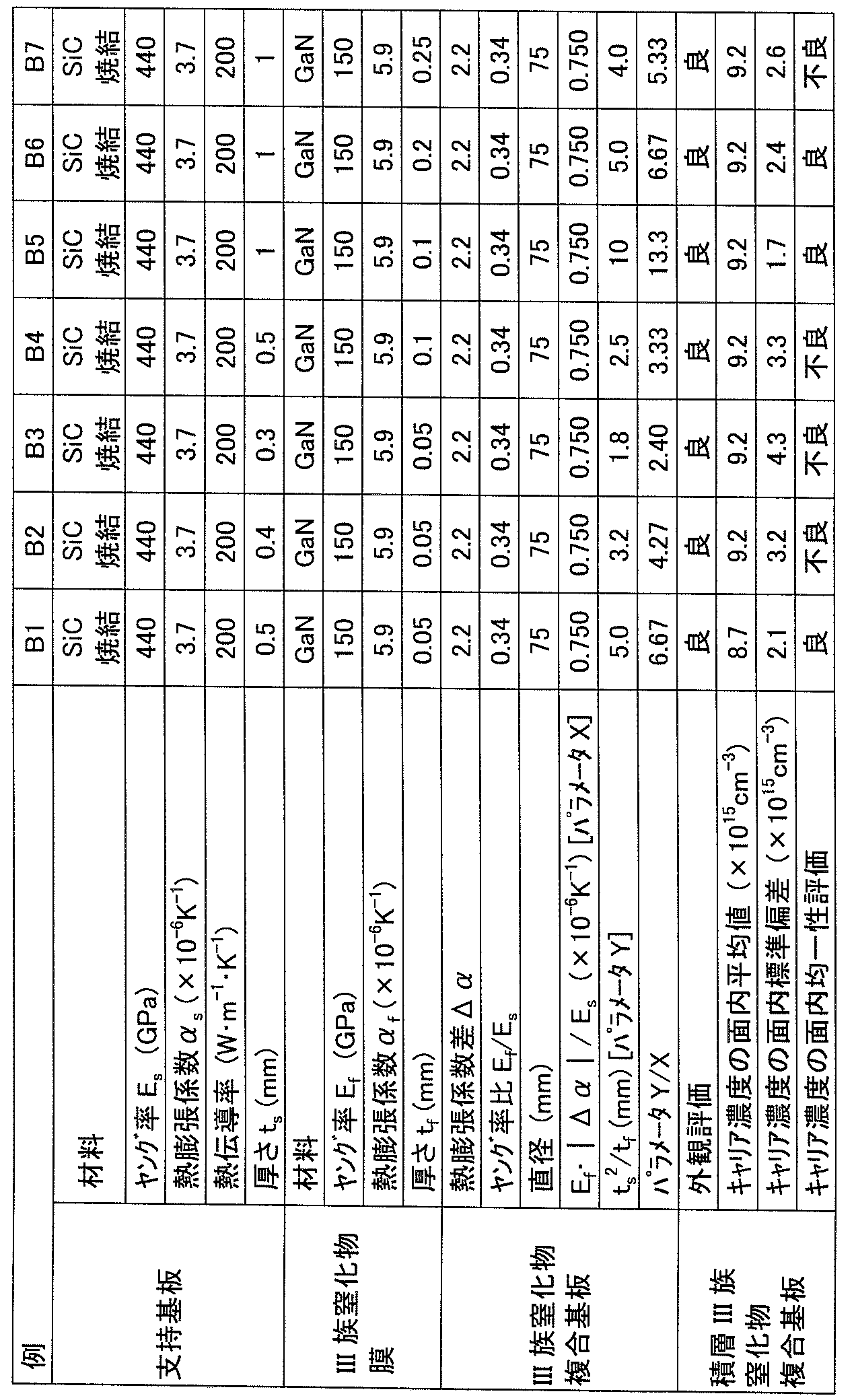
表2を参照して、例B1~例B7の全ての例において、積層III族窒化物複合基板のIII族窒化物膜およびIII族窒化物層にクラックおよび剥がれがなく外観が良であった。また、積層III族窒化物複合基板のIII族窒化物層のキャリアドリフト層のキャリア濃度の主面に平行な面内の均一性は、支持基板の厚さが小さい例B2および例B3、ならびに、支持基板の厚さに対してIII族窒化物膜の厚さが大きい例B4および例B7について不良であり、支持基板の厚さが大きくIII族窒化物膜の厚さが小さい例B1、ならびに、支持基板の厚さが大きい例B5~例B6について良であった。
(実施例C)
Siを材料とする支持基板を用いて、支持基板の厚さおよびIII族窒化物膜の厚さが表3の例C1~例C5に示すように異なるIII族窒化物複合基板を作製したこと以外は、実施例Aと同様にして、III族窒化物複合基板を作製し、III族窒化物複合基板のIII族窒化物膜上にIII族窒化物層を成長させて積層III族窒化物複合基板を作製した。また、得られた積層III族窒化物複合基板の外観およびキャリア濃度の面内均一性を評価した。結果を表3にまとめた。
Siを材料とする支持基板を用いて、支持基板の厚さおよびIII族窒化物膜の厚さが表3の例C1~例C5に示すように異なるIII族窒化物複合基板を作製したこと以外は、実施例Aと同様にして、III族窒化物複合基板を作製し、III族窒化物複合基板のIII族窒化物膜上にIII族窒化物層を成長させて積層III族窒化物複合基板を作製した。また、得られた積層III族窒化物複合基板の外観およびキャリア濃度の面内均一性を評価した。結果を表3にまとめた。
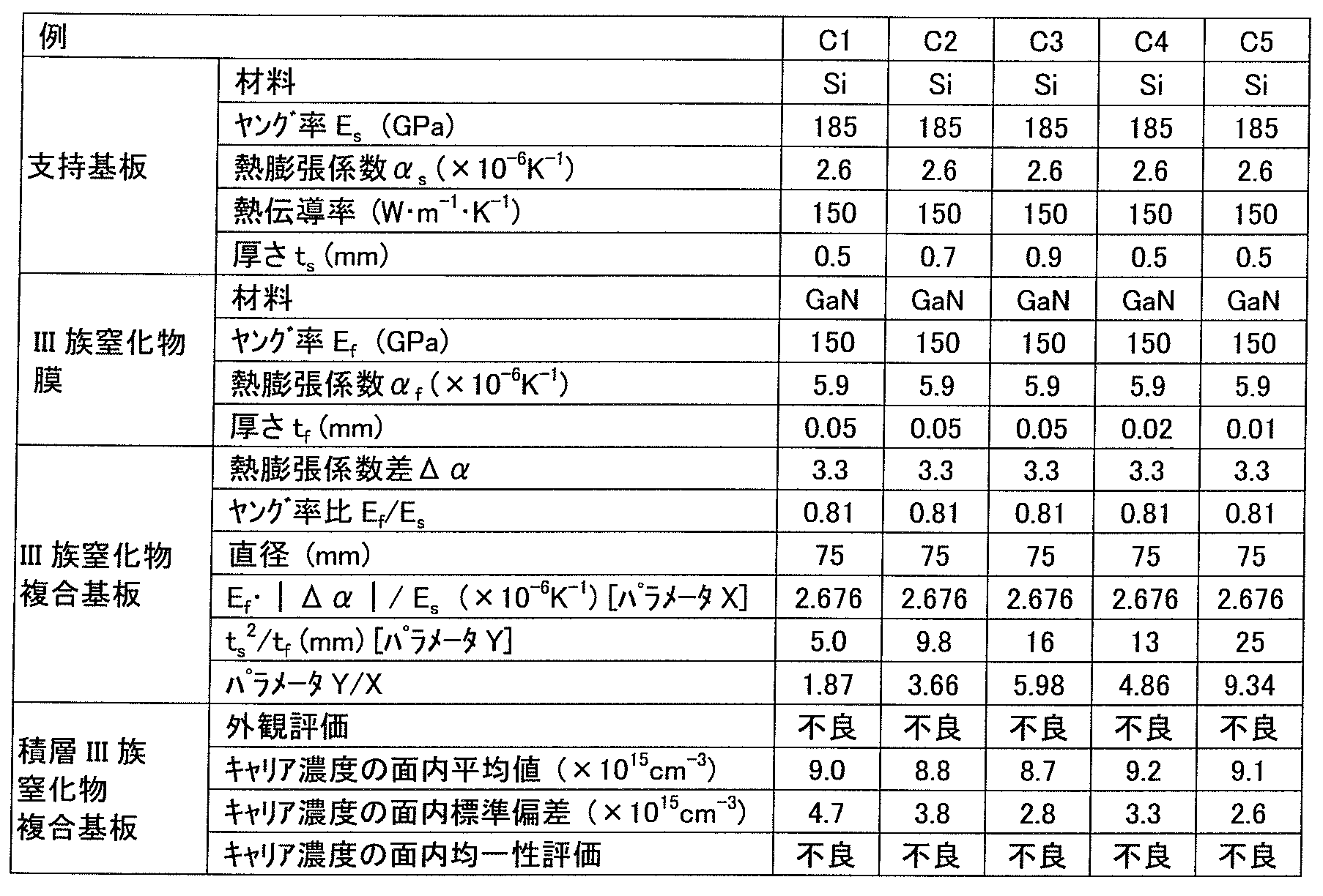
表3を参照して、例C1~例C5の全ての例において、積層III族窒化物複合基板のIII族窒化物膜およびIII族窒化物層にクラックが発生して外観が不良となった。これは、支持基板とIII族窒化物膜との間の熱膨張係数差が大きかったためと考えられた。また、積層III族窒化物複合基板のIII族窒化物層のキャリアドリフト層のキャリア濃度の主面に平行な面内の均一性は、例C1~例C5の全ての例において、外周部の上記クラックの発生部分においてキャリア濃度の異常分布が発生し、不良となった。
(実施例D)
基板全体に対してAl2O3が85質量%でSiO2が15質量%のAl2O3-SiO2複合酸化物を材料とする支持基板を用いて、支持基板の厚さ、III族窒化物膜の厚さ、およびIII族窒化物複合基板の直径が表4の例D1~例D10に示すように異なるIII族窒化物複合基板を作製したこと以外は、実施例Aと同様にして、III族窒化物複合基板を作製し、III族窒化物複合基板のIII族窒化物膜上にIII族窒化物層を成長させて積層III族窒化物複合基板を作製した。また、得られた積層III族窒化物複合基板の外観およびキャリア濃度の面内均一性を評価した。結果を表4にまとめた。
基板全体に対してAl2O3が85質量%でSiO2が15質量%のAl2O3-SiO2複合酸化物を材料とする支持基板を用いて、支持基板の厚さ、III族窒化物膜の厚さ、およびIII族窒化物複合基板の直径が表4の例D1~例D10に示すように異なるIII族窒化物複合基板を作製したこと以外は、実施例Aと同様にして、III族窒化物複合基板を作製し、III族窒化物複合基板のIII族窒化物膜上にIII族窒化物層を成長させて積層III族窒化物複合基板を作製した。また、得られた積層III族窒化物複合基板の外観およびキャリア濃度の面内均一性を評価した。結果を表4にまとめた。
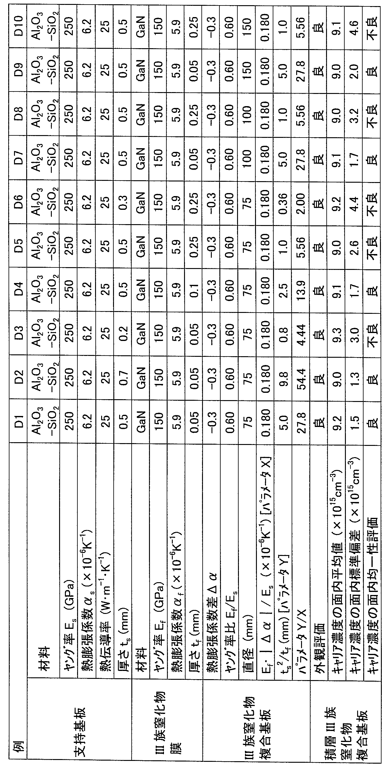
表4を参照して、例D1~例D10の全ての例において、積層III族窒化物複合基板のIII族窒化物膜およびIII族窒化物層にクラックおよび剥がれがなく外観が良であった。また、積層III族窒化物複合基板のIII族窒化物層のキャリアドリフト層のキャリア濃度の主面に平行な面内の均一性は、支持基板の厚さが小さい例D3、ならびに、III族窒化物膜の厚さが大きい例D5、例D6、例D8、および例D10について不良であり、支持基板の厚さが大きくIII族窒化物膜の厚さが小さい例D1、例D2、例D4、D7および例D9について良であった。
(実施例E)
表5の例E1~例E11のそれぞれに示す材料、直径および厚さの支持基板を準備した。各例における支持基板は、例E1、例E6および例E9が主面を鏡面仕上げ(RMSが10nm以下)したMo基板であり、例E2、例E7および例E10が主面を鏡面仕上げ(RMSが10nm以下)したW基板であり、例E3、例E8および例E11が比抵抗100μΩcmのZrB2基板であり、例E4が比抵抗1mΩcmのSi基板であり、例E5が比抵抗10mΩcmのSiC基板であった。支持基板およびIII族窒化物膜ドナー基板の両方の貼り合わせ主面にスパッタ法により、接合膜として比抵抗が10mΩcmの高導電性のGa2O3膜を形成したこと以外は、実施例Aと同様にして、III族窒化物複合基板を作製し、III族窒化物複合基板のIII族窒化物膜上にIII族窒化物層を成長させて積層III族窒化物複合基板を作製した。また、得られた積層III族窒化物複合基板の外観およびキャリア濃度の面内均一性を評価した。結果を表5にまとめた。
表5の例E1~例E11のそれぞれに示す材料、直径および厚さの支持基板を準備した。各例における支持基板は、例E1、例E6および例E9が主面を鏡面仕上げ(RMSが10nm以下)したMo基板であり、例E2、例E7および例E10が主面を鏡面仕上げ(RMSが10nm以下)したW基板であり、例E3、例E8および例E11が比抵抗100μΩcmのZrB2基板であり、例E4が比抵抗1mΩcmのSi基板であり、例E5が比抵抗10mΩcmのSiC基板であった。支持基板およびIII族窒化物膜ドナー基板の両方の貼り合わせ主面にスパッタ法により、接合膜として比抵抗が10mΩcmの高導電性のGa2O3膜を形成したこと以外は、実施例Aと同様にして、III族窒化物複合基板を作製し、III族窒化物複合基板のIII族窒化物膜上にIII族窒化物層を成長させて積層III族窒化物複合基板を作製した。また、得られた積層III族窒化物複合基板の外観およびキャリア濃度の面内均一性を評価した。結果を表5にまとめた。

表5を参照して、支持基板とIII族窒化物膜との間の熱膨張係数差Δαの絶対値が大きい例E4において、積層III族窒化物複合基板のIII族窒化物膜およびIII族窒化物層にクラックが発生し外観が不良であった。支持基板とIII族窒化物膜との間の熱膨張係数差Δαの絶対値が小さい例E1~例E3および例E5~例E11において、積層III族窒化物複合基板のIII族窒化物膜およびIII族窒化物層にクラックおよび剥がれがなく外観が良好であった。また、積層III族窒化物複合基板のIII族窒化物層のキャリアドリフト層のキャリア濃度の主面に平行な面内の均一性は、上記と同様に、例E4について不良であり、例E1~例E3および例E5~例E11について良であった。ここで、支持基板の材料種によって上記の傾向に大小が見られた。
(実施例F)
支持基板として主面を鏡面仕上げ(RMSが10nm以下)したMo基板または主面を鏡面仕上げ(RMSが10nm以下)したW基板を用いて、支持基板の厚さおよびIII族窒化物膜の厚さが表6の例F1~例F10に示すように異なる直径75mmのIII族窒化物複合基板を作製したこと以外は、実施例Eと同様にして、III族窒化物複合基板を作製し、III族窒化物複合基板のIII族窒化物膜上にIII族窒化物層を成長させて積層III族窒化物複合基板を作製した。また、得られた積層III族窒化物複合基板の外観およびキャリア濃度の面内均一性を評価した。結果を表6にまとめた。
支持基板として主面を鏡面仕上げ(RMSが10nm以下)したMo基板または主面を鏡面仕上げ(RMSが10nm以下)したW基板を用いて、支持基板の厚さおよびIII族窒化物膜の厚さが表6の例F1~例F10に示すように異なる直径75mmのIII族窒化物複合基板を作製したこと以外は、実施例Eと同様にして、III族窒化物複合基板を作製し、III族窒化物複合基板のIII族窒化物膜上にIII族窒化物層を成長させて積層III族窒化物複合基板を作製した。また、得られた積層III族窒化物複合基板の外観およびキャリア濃度の面内均一性を評価した。結果を表6にまとめた。
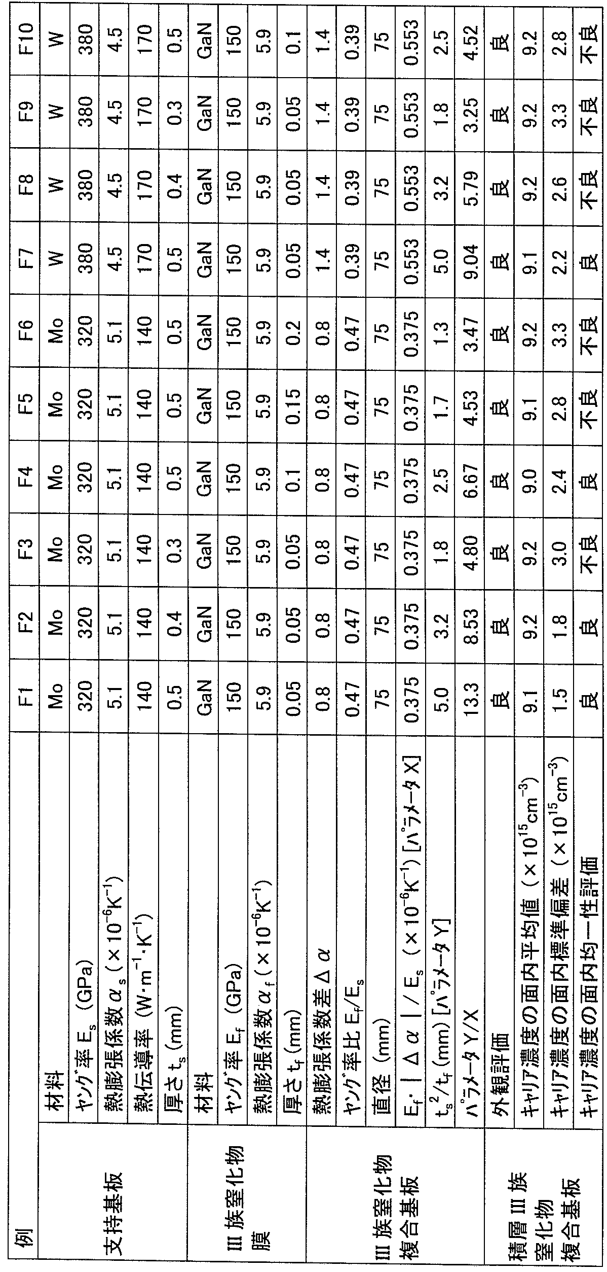
表6を参照して、例F1~例F10の全ての例において、積層III族窒化物複合基板のIII族窒化物膜およびIII族窒化物層にクラックおよび剥がれがなく外観が良であった。また、積層III族窒化物複合基板のIII族窒化物層のキャリアドリフト層のキャリア濃度の主面に平行な面内の均一性は、支持基板の厚さが小さい例F3、例F8および例F9、ならびに、III族窒化物膜の厚さが大きい例F5および例F6について不良であり、支持基板の厚さが大きくIII族窒化物膜の厚さが小さい例F1、例F2、例F4および例F7について良であった。ここで、支持基板の材料種によって上記の傾向に大小が見られた。
(実施例A~実施例Fからの考察)
上記の実施例A~実施例Fで示したように、支持基板の材料種および厚さならびにIII族窒化物膜の厚さによって、III族窒化物複合基板のIII族窒化物膜上にIII族窒化物層を成長させて形成した積層III族窒化物複合基板の外観およびIII族窒化物層のキャリア濃度の主面に平行な面内分布の均一性が変化する結果となった。
上記の実施例A~実施例Fで示したように、支持基板の材料種および厚さならびにIII族窒化物膜の厚さによって、III族窒化物複合基板のIII族窒化物膜上にIII族窒化物層を成長させて形成した積層III族窒化物複合基板の外観およびIII族窒化物層のキャリア濃度の主面に平行な面内分布の均一性が変化する結果となった。
これらの結果から、上記の積層III族窒化物複合基板の外観およびIII族窒化物層のキャリア濃度の主面に平行な面内分布の均一性について、以下のように考察した。
1.積層III族窒化物複合基板の外観について
積層III族窒化物複合基板の外観、特に、積層III族窒化物複合基板のIII族窒化物層およびIII族窒化物膜のクラックの発生および支持基板からの剥がれの有無に関して、III族窒化物複合基板のIII族窒化物膜上へのIII族窒化物層のエピタキシャル成長の際にIII族窒化物複合基板にかかる熱応力の観点から、以下のように考察した。
積層III族窒化物複合基板の外観、特に、積層III族窒化物複合基板のIII族窒化物層およびIII族窒化物膜のクラックの発生および支持基板からの剥がれの有無に関して、III族窒化物複合基板のIII族窒化物膜上へのIII族窒化物層のエピタキシャル成長の際にIII族窒化物複合基板にかかる熱応力の観点から、以下のように考察した。
上記実施例のIII族窒化物複合基板は、支持基板とIII族窒化物膜ドナー基板とを接合膜を介在させて貼り合わせた後、貼り合わせ強度を高めるため800℃でアニールされた際に熱応力を受け、さらにIII族窒化物複合基板のIII族窒化物膜上に1050℃でIII族窒化物層をエピタキシャル成長させた際にさらに大きな熱応力を受けたものであった。そして、一部の積層III族窒化物複合基板においては、かかる熱応力によりIII族窒化物層およびIII族窒化物膜にクラックおよび支持基板からの剥がれが発生したと考えられた。
かかる熱応力σT(単位:Pa)は、III族窒化物膜13の熱膨張係数αf(単位:×10-6K-1)から支持基板11の熱膨張係数αS(単位:×10-6K-1)を引いた熱膨張係数差Δα(単位:×10-6K-1)により発生し、III族窒化物膜13の厚さtf(単位:mm)が支持基板11の厚さts(単位:mm)に比べて小さいと仮定して、III族窒化物膜13のヤング率Ef(単位:GPa)、ポアソン比νf(単位:無次元)、III族窒化物層の成長温度Tg(単位:℃)からIII族窒化物複合基板1の形成温度Tb(単位:℃)(具体的には、III族窒化物複合基板の形成の際のアニール温度)を引いた温度差ΔT(単位:℃)、および上記熱膨張係数差Δαを用いて、次の式(2)
σT=Ef・|Δα・|ΔT/(1-νf) ・・・(2)
で表わされた。すなわち、支持基板とIII族窒化物膜との間の熱膨張係数差Δαが熱応力σTを決定する重要な因子であることがわかった。
σT=Ef・|Δα・|ΔT/(1-νf) ・・・(2)
で表わされた。すなわち、支持基板とIII族窒化物膜との間の熱膨張係数差Δαが熱応力σTを決定する重要な因子であることがわかった。
そこで、上記実施例A~実施例Fの各例について、上記熱膨張係数差Δαに対して積層III族窒化物複合基板の外観の良否をプロットした。結果を図18に示した。図18から明らかなように、熱膨張係数差Δαの絶対値|Δα|が2.2×10⁻⁶K-1以下の支持基板およびIII族窒化物膜を含むIII族窒化物複合基板を用いることにより、III族窒化物層およびIII族窒化物膜のクラックおよび支持基板からの剥がれが発生しないことがわかった。ここで、Δα>0の場合は、III族窒化物層の成長温度での複合基板の変形方向が、III族窒化物膜13側に凸状になった。Δα<0の場合は、III族窒化物層の成長温度での複合基板の変形方向が、III族窒化物膜13側に凹状になった。図18の結果は、変形方向(すなわちΔαの正負)に依らず、Δαの絶対値|Δα|が2.2×10⁻⁶K-1以下であれば、III族窒化物層成長後にクラックや剥がれの発生しないことを示していた。
2.III族窒化物層のキャリア濃度の主面に平行な面内分布の均一性について
III族窒化物層のキャリア濃度の主面に平行な面内分布の均一性は、支持基板の材料種および厚さならびにIII族窒化物膜の厚さなどによって大きく変化した。また、III族窒化物層のキャリア濃度の主面に平行な面内分布は、いずれの例においても同心円状に変化した。
III族窒化物層のキャリア濃度の主面に平行な面内分布の均一性は、支持基板の材料種および厚さならびにIII族窒化物膜の厚さなどによって大きく変化した。また、III族窒化物層のキャリア濃度の主面に平行な面内分布は、いずれの例においても同心円状に変化した。
このため、III族窒化物層のキャリア濃度の主面に平行な面内分布は、III族窒化物複合基板のIII族窒化物膜上にIII族窒化物層をエピタキシャル成長させる際のIII族窒化物複合基板の反りによって生じたものと考えた。すなわち、III族窒化物複合基板の反りに伴うIII族窒化物膜の表面の温度分布およびガス流の乱れが、上記キャリア濃度の面内分布に影響を及ぼすものと考えた。
したがって、III族窒化物複合基板のIII族窒化物膜上に少なくとも1層のIII族窒化物層を成長させる際のIII族窒化物複合基板1の反りによる曲率半径R(単位:m)は、支持基板のヤング率Es(単位:GPa)および厚さts(単位:mm)、III族窒化物膜の厚さtf(単位:mm)ならびに熱応力σT(単位:Pa)を用いて、Stoneyの式から、次の式(3)
R=Es/{6(1-νs)σT}・ts 2/tf ・・・(3)
で表わされた。
R=Es/{6(1-νs)σT}・ts 2/tf ・・・(3)
で表わされた。
次に、式(2)を式(3)に代入することにより、次の式(4)
R=Es/{Ef・|Δα|・ΔT}/{6(1-νs)/(1-νf)}・ts 2/tf ・・・(4)
が得られた。かかる式(4)は、次式(5)
ts 2/tf=[RΔT(1-νf)/6(1-νs)]Ef・|Δα|/Es ・・・(5)
と変形された。かかる式(5)は、支持基板およびIII族窒化物膜のヤング率および熱膨張係数差に関するパラメータXとしてのEf・|Δα|/Esに対して支持基板およびIII族窒化物の厚さに関するパラメータYとしてのts 2/tfが所定の関係を有することを示していた。
R=Es/{Ef・|Δα|・ΔT}/{6(1-νs)/(1-νf)}・ts 2/tf ・・・(4)
が得られた。かかる式(4)は、次式(5)
ts 2/tf=[RΔT(1-νf)/6(1-νs)]Ef・|Δα|/Es ・・・(5)
と変形された。かかる式(5)は、支持基板およびIII族窒化物膜のヤング率および熱膨張係数差に関するパラメータXとしてのEf・|Δα|/Esに対して支持基板およびIII族窒化物の厚さに関するパラメータYとしてのts 2/tfが所定の関係を有することを示していた。
そこで、支持基板およびIII族窒化物膜の材料特性(ヤング率および熱膨張係数)に関係するEf・|Δα|/Es(パラメータX)ならびに支持基板およびIII族窒化物膜の厚さに関係するts
2/tf(パラメータY)に対して、III族窒化物層のキャリア濃度の主面に平行な面内分布の均一性の良否をプロットした。結果を図19に示した。図19において、キャリア濃度の面内標準偏差が2.5×1015cm-3以下のものをキャリア濃度の面内分布の均一性が良として○印をプロットし、キャリア濃度の面内標準偏差が2.5×1015cm-3より大きいものをキャリア濃度の面内分布の均一性が不良として×印をプロットした。
図19を参照して、Ef・|Δα|/Es(パラメータX)とts
2/tf(パラメータY)とが、
ts 2/tf≧6Ef・|Δα|/Es ・・・(1)
の関係を満たすときに、III族窒化物層20のキャリア濃度の主面に平行な面内における分布の均一性がよいことがわかった。
ts 2/tf≧6Ef・|Δα|/Es ・・・(1)
の関係を満たすときに、III族窒化物層20のキャリア濃度の主面に平行な面内における分布の均一性がよいことがわかった。
3.支持基板およびIII族窒化物膜の厚さについて
支持基板の厚さtsおよびIII族窒化物膜の厚さtfは、上記式(1)を満たすように設計することにより、III族窒化物層のキャリア濃度の主面に平行な面内における分布の均一性がよくなることがわかった。
支持基板の厚さtsおよびIII族窒化物膜の厚さtfは、上記式(1)を満たすように設計することにより、III族窒化物層のキャリア濃度の主面に平行な面内における分布の均一性がよくなることがわかった。
また、支持基板の厚さtsは、III族窒化物複合基板の機械的強度が高くハンドリング性がよい観点から0.1mm以上が適当であり、III族窒化物複合基板のコストを低減しハンドリング性がよい観点から1mm以下が適当であることがわかった。
(実施例G)
本実施例は、図14を参照して、デバイス支持基板40を含むIII族窒化物半導体デバイス4であるSBD(ショットキーバリアダイオード)を作製した実施例である。
本実施例は、図14を参照して、デバイス支持基板40を含むIII族窒化物半導体デバイス4であるSBD(ショットキーバリアダイオード)を作製した実施例である。
1.III族窒化物複合基板の作製
支持基板として基板全体に対してAl2O3が85質量%でSiO2が15質量%のAl2O3-SiO2複合酸化物基板を用いて、支持基板の厚さおよびIII族窒化物複合基板の直径が表7の例G1~例G8に示すように異なるIII族窒化物複合基板を作製したこと以外は、実施例Aと同様にしてIII族窒化物複合基板を作製した。
支持基板として基板全体に対してAl2O3が85質量%でSiO2が15質量%のAl2O3-SiO2複合酸化物基板を用いて、支持基板の厚さおよびIII族窒化物複合基板の直径が表7の例G1~例G8に示すように異なるIII族窒化物複合基板を作製したこと以外は、実施例Aと同様にしてIII族窒化物複合基板を作製した。
2.III族窒化物半導体デバイスの作製
図14(A)を参照して、実施例Aと同様にして、III族窒化物複合基板1のIII族窒化物膜13上に、III族窒化物層20として、キャリアストップ層であるキャリア濃度が2×1018cm-3で厚さが1μmのn+-GaN層201、およびキャリアドリフト層であるキャリア濃度が1×1016cm-3で厚さが5μmのn--GaN層202を順にエピタキシャル成長された積層III族窒化物複合基板2を作製した。
図14(A)を参照して、実施例Aと同様にして、III族窒化物複合基板1のIII族窒化物膜13上に、III族窒化物層20として、キャリアストップ層であるキャリア濃度が2×1018cm-3で厚さが1μmのn+-GaN層201、およびキャリアドリフト層であるキャリア濃度が1×1016cm-3で厚さが5μmのn--GaN層202を順にエピタキシャル成長された積層III族窒化物複合基板2を作製した。
得られた積層III族窒化物複合基板の外観およびキャリア濃度の面内均一性を、実施例Aと同様にして、評価した。例G1~例G8の全ての例において、積層III族窒化物複合基板のIII族窒化物膜およびIII族窒化物層にクラックおよび剥がれがなく外観が良であり、キャリア濃度の面内均一性も良であった。結果を表7にまとめた。
次に、図14(B)を参照して、積層III族窒化物複合基板2のIII族窒化物層20の最上層であるn--GaN層202上に、フィールドプレート用の絶縁膜300として、プラズマCVD法により、SiH4およびNH3を原料として用いて、厚さ500nmのSiNx膜を形成した。その後、RTA(高速熱処理装置)を用いてN2中600℃で3分間熱処理した。次に、フォトリソグラフィで形成したレジストマスクを用いて、バッファードフッ酸(50質量%のHF(フッ化水素酸)水溶液と40質量%のNH4F(フッ化アンモニウム)水溶液とを1:5の体積比で混合したもの。以下同じ。)で15分間エッチングし、レジストマスク開口部のSiNx膜を除去することにより、フィールドプレートとして開口部を有する絶縁膜300を形成した。ここで、絶縁膜300の各開口部の平面形状は1mm角であった。上記のエッチング後、アセトンを用いてレジストを除去した。
次に、フォトリソグラフィでレジストマスク(図示せず)を形成し、EB蒸着法により、厚さ50nmのNi層および厚さ300nmのAu層を形成し、アセトン中でリフトオフすることにより、第1電極30としてパターン化されたショットキー電極を形成した。第1電極30である各ショットキー電極の平面形状は1.1mm角であり、絶縁膜300の開口部のn--GaN層202上および絶縁膜300の開口部の周囲から絶縁膜300側に50μmまでの範囲上において第1電極30が配置されたフィールドプレート耐圧構造とした。
次に、図14(C)を参照して、第1電極30および絶縁膜300上の全面に、EB蒸着法により、バリア膜330として、厚さ50nmのNi層、厚さ400nmのPt層および厚さ100nmのAu層を形成した。かかるバリア膜330は、この後のデバイス支持基板40を貼り合わせる工程において、接合金属膜44中の金属原子の拡散などによるショットキー特性の劣化を防止することができる。
次に、デバイス支持基板40上に、EB蒸着法により、オーミック電極となるパッド電極43として、厚さ50nmのNi層、厚さ400nmのPt層および厚さ100nmのAu層を形成した。さらに、パッド電極43上に、抵抗加熱蒸着法により、接合金属膜44として、厚さ5μmのAuSn膜(Auが70質量%でSnが30質量%)を形成した。
ここで、デバイス支持基板40としては、例G1および例G2においては、ヤング率が185GPa、熱膨張係数が2.6×10-6K-1、熱伝導率が150W・m-1・K-1、および比抵抗が1mΩcmのSi基板を用いた。例G3および例G6においては、基板全体に対してCuが6質量%でWが94質量%で、ヤング率が350GPa、熱膨張係数が6.0×10⁻⁶K-1、熱伝導率が130W・m-1・K-1、および比抵抗が0.1μΩcmのCuW基板を用いた。例G4においては、基板全体に対してCuが60体積%でダイヤモンドが40体積%で、ヤング率が410GPa、熱膨張係数が6.0×10⁻⁶K-1、熱伝導率が560W・m-1・K-1、および比抵抗が500μΩcmのCu-ダイヤモンド基板を用いた。例G5においては、基板全体に対してFeが54質量%でNiが29質量%でCoが17質量%で、ヤング率が140GPa、熱膨張係数が5.3×10⁻⁶K-1、熱伝導率が17W・m-1・K-1、および比抵抗が100μΩcmのコバール(Kovar)基板を用いた。例G7においては、ヤング率が320GPa、熱膨張係数が5.1×10⁻⁶K-1、熱伝導率が140W・m-1・K-1、および比抵抗が5.7μΩcmのMo基板を用いた。例G8においては、ヤング率が380GPa、熱膨張係数が4.5×10-6K-1、熱伝導率が10W・m-1・K-1、および比抵抗が5.4μΩcmのW基板を用いた。
次に、ウエハボンダを用いて、上記接合金属膜44と上記バリア膜330とを接合させた。接合条件は、1Pa未満の真空雰囲気中300℃で10分間とした。接合後、超音波顕微鏡により接合面の状態を観察した。例G1~例G8の全ての例において、ボイドの発生などの接合面不良は認められなかった。こうして、積層基板3が得られた。
次に、図14(D1)を参照して、平面研削機を用いて、積層基板3の支持基板11をその露出している主面から研削して、厚さを50μmとした。次いで、積層基板3からIII族窒化物複合基板1の支持基板11および接合膜12を、フッ化水素酸を用いて、エッチングにより除去した。その後、積層基板3から支持基板11および接合膜12が除去されて露出したIII族窒化物膜13を、ICP-RIE(誘導結合プラズマ-反応性イオンエッチング)法により、Cl2をエッチングガスとして用いて、その露出した主面から200nmの深さまでエッチングした。
次に、図14(E1)を参照して、III族窒化物膜13上に、EB蒸着法により、厚さ20nmのTi層、厚さ100nmのAl層、厚さ20nmのTi層および厚さ300nmのAu層を順次形成することにより、第2電極50であるオーミック電極を、第1電極30であるオーミック電極の位置に合わせてリフトオフ法により平面形状が1.4mm角で形成した。また、デバイス支持基板40がSi基板の場合、デバイス支持基板40上に、EB蒸着法により、平面形状が1.4mm角で、厚さ10nmのNi層、厚さ10nmのPt層および厚さ100nmのAu層を順次形成することにより、デバイス支持基板電極45であるオーミック電極を形成した。
次に、第1電極30および第2電極50などが形成されたIII族窒化物半導体デバイス4を、RTAを用いて、N2雰囲気中250℃で3分間アニールした。こうして、III族窒化物半導体デバイス4が得られた。
得られたIII族窒化物半導体デバイス4を、以下のようにしてチップ化した。デバイス支持基板40としてSi基板を含むIII族窒化物半導体デバイス4は、その第2電極50側を下にしてUV(紫外線)硬化性ダイシングテープに貼り付けて、ダイサーを用いて、上記電極のパターンに合わせて、平面形状が1.5mm角で、デバイス支持基板40、III族窒化物層20およびIII族窒化物膜13をダイシングすることにより、チップ化した。
各III族窒化物半導体デバイスの主面上の外周部5mmを除く全面から上記のチップ化により得られるIII族窒化物半導体デバイスの全個数は、直径75mmの基板からは150個、直径100mmの基板からは300個、直径150mmの基板からは700個であった。
上記のようにして得られたチップ化されたIII族窒化物半導体デバイスについて、プローバーを用いて、電流-電圧特性測定を行なった。順方向特性の指標は電流密度が500A/cm2となるときの順方向電圧Vfとし、逆方向特性の指標は電流密度が1×10-3A/cm2となるときの逆方向耐電圧Vrとした。ここで、III族窒化物半導体デバイスがSBDの場合は、順方向電圧Vfが1.5V以下でかつ逆方向耐電圧Vrが500V以上のIII族窒化物半導体デバイスを良品とした。III族窒化物半導体デバイスの全個数に対して、順方向電圧Vfが1.5V以下となるIII族窒化物半導体デバイスの個数の割合をVf歩留といい、逆方向耐電圧Vrが500V以上となるIII族窒化物半導体デバイスの個数の割合をVr歩留という。得られたチップ化されたIII族窒化物半導体デバイスの特性値を表7にまとめた。
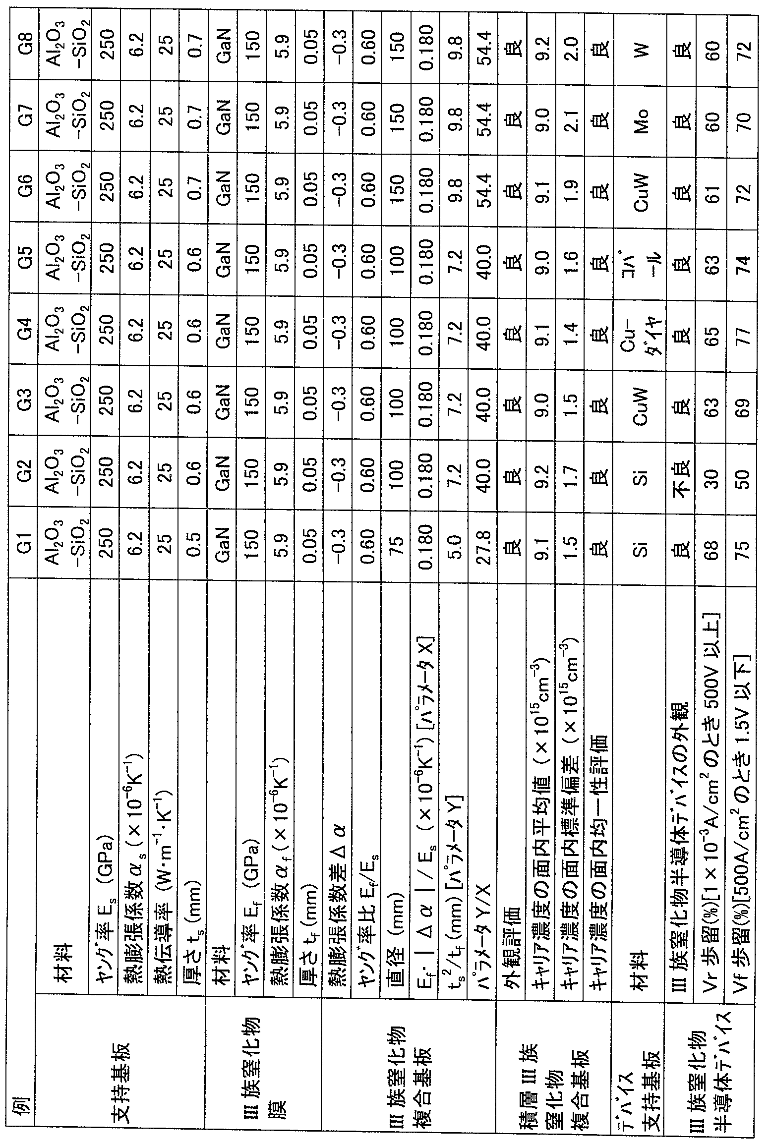
表7を参照して、例G1および例G2に示すように、支持基板としてSi基板を用いたIII族窒化物半導体デバイスにおいては、直径が75mmのときはVf歩留およびVr歩留が60%以上と高かったが、直径が100mmのときはデバイス支持基板との貼り合わせ後にデバイス支持基板からのIII族窒化物層およびIII族窒化物膜の一部剥離が発生してVf歩留およびVr歩留が50%以下と低くなった。例G3~例G8に示すように、支持基板として、直径が100mmであるCuW基板、Cu-ダイヤモンド基板あるいはコバール(Kovar)基板、直径が150mmであるCuW基板、Mo基板あるいはW基板を用いた場合は、デバイス支持基板へのIII族窒化物層およびIII族窒化物膜の貼り合わせは全面に亘って良好であり、Vf歩留およびVr歩留が60%以上と高かった。
(実施例H)
本実施例は、図15を参照して、支持基板11を含むIII族窒化物半導体デバイス4であるSBDを作製した実施例である。
本実施例は、図15を参照して、支持基板11を含むIII族窒化物半導体デバイス4であるSBDを作製した実施例である。
1.III族窒化物複合基板の作製
支持基板として主面を鏡面仕上げ(RMSが10nm以下)したMo基板またはW基板を用いて、支持基板の厚さおよびIII族窒化物膜の厚さが表8の例H1~例H4および例H6~例H8に示すように異なる直径75mmのIII族窒化物複合基板を作製したこと以外は、実施例Eと同様にして、III族窒化物複合基板を作製した。
支持基板として主面を鏡面仕上げ(RMSが10nm以下)したMo基板またはW基板を用いて、支持基板の厚さおよびIII族窒化物膜の厚さが表8の例H1~例H4および例H6~例H8に示すように異なる直径75mmのIII族窒化物複合基板を作製したこと以外は、実施例Eと同様にして、III族窒化物複合基板を作製した。
また、例H5については、図13を参照して、支持基板11として上記Mo基板を用いて、図13(B)に示すように、III族窒化物膜ドナー基板13Dである所定の直径を有するGaN結晶体にその主面から内部に所定の深さの位置に水素イオンを注入することによりイオン注入領域13iを形成した後、図13(C)に示すように、支持基板11とIII族窒化物膜ドナー基板13Dのイオン注入領域13i側とを接合膜12を介在させて貼り合わせた後、図13(D)に示すように、850℃でアニールすることにより、III族窒化物膜ドナー基板13Dをそのイオン注入領域13iで分離し、その分離面を研磨することにより、III族窒化物膜13の厚さが0.0005mmのIII族窒化物複合基板を作製した。
2.III族窒化物半導体デバイスの作製
図15(A)を参照して、実施例Aと同様にして、III族窒化物複合基板1のIII族窒化物膜13上に、III族窒化物層20として、キャリアストップ層であるキャリア濃度が2×1018cm-3で厚さが1μmのn+-GaN層201、およびキャリアドリフト層であるキャリア濃度が1×1016cm-3で厚さが5μmのn--GaN層202を順にエピタキシャル成長された積層III族窒化物複合基板2を作製した。
図15(A)を参照して、実施例Aと同様にして、III族窒化物複合基板1のIII族窒化物膜13上に、III族窒化物層20として、キャリアストップ層であるキャリア濃度が2×1018cm-3で厚さが1μmのn+-GaN層201、およびキャリアドリフト層であるキャリア濃度が1×1016cm-3で厚さが5μmのn--GaN層202を順にエピタキシャル成長された積層III族窒化物複合基板2を作製した。
得られた積層III族窒化物複合基板の外観およびキャリア濃度の面内均一性を、実施例Aと同様にして、評価した。例H1~例H8の全ての例において、積層III族窒化物複合基板のIII族窒化物膜およびIII族窒化物層にクラックおよび剥がれがなく外観が良であった。キャリア濃度の面内均一性については、III族窒化物膜の厚さが大きいまたは支持基板の厚さが小さい例H3、例H4、例H7および例H8では不良となり、それ以外の例H1、例H2、例H5および例H6では良となった。結果を表8にまとめた。
次に、図15(B)を参照して、実施例Gと同様にして、III族窒化物層20のn--GaN層202側に開口部を有する絶縁膜300およびショットキー電極である第1電極を30を順次形成することにより、III族窒化物半導体デバイス4を作製した。なお、図15(B)には、支持基板11上にはオーミック電極である第2電極50が形成されているが、本実施例において支持基板11として用いられるMo基板およびW基板はいずれもオーミック電極としても機能するため、支持基板11に第2電極50を設けなかった。
次に、得られたIII族窒化物半導体デバイスを、実施例Gと同様にして、チップ化した。各III族窒化物半導体デバイスの主面上の外周部5mmを除く全面から得られた150個のチップ化されたIII族窒化物半導体デバイスについて、実施例Gと同様にして、Vf歩留およびVr歩留を求めた。得られたチップ化されたIII族窒化物半導体デバイスの特性値を表8にまとめた。
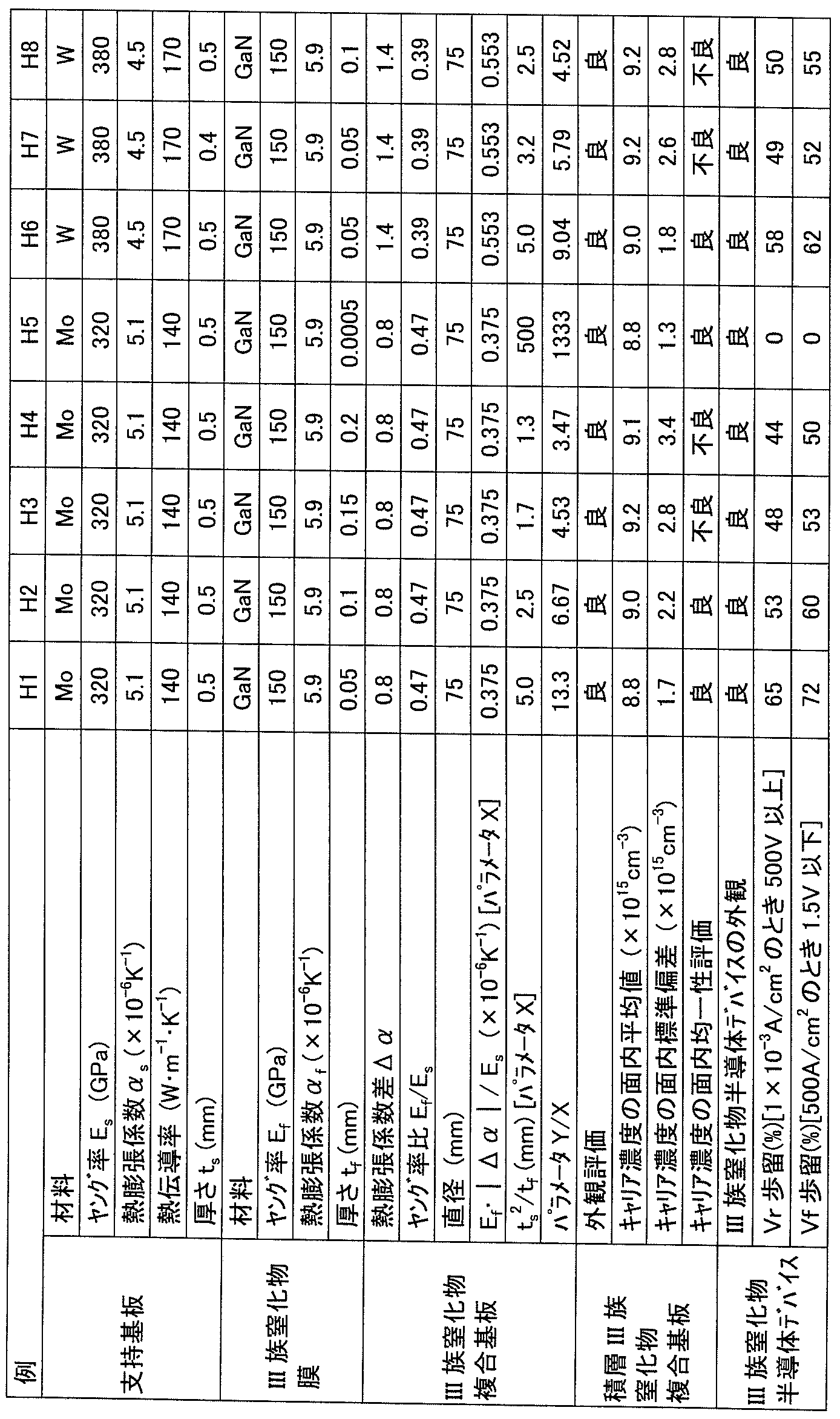
表8を参照して、支持基板としてMo基板を用いたIII族窒化物半導体デバイスにおいては、例H1および例H2に示すように、III族窒化物膜の厚さがそれぞれ0.05mmおよび0.1mmのとき、III族窒化物層のキャリア濃度の面内均一性が良でありVf歩留およびVr歩留が高かったが、例H3および例H4に示すように、III族窒化物膜の厚さがそれぞれ0.15mmおよび0.2mmと大きいとき、III族窒化物層のキャリア濃度の面内均一性が不良でありVf歩留およびVr歩留が低かった。
また、例H5に示すように、III族窒化物膜の厚さが0.0005mmと極めて小さいとき、III族窒化物層のキャリア濃度の面内均一性が良であったが、Vf歩留およびVr歩留がいずれも0となった。これは、例H5のIII族窒化物半導体デバイスのIII族窒化物膜は、水素イオンの注入により、結晶品質が低下したとともに高抵抗層が形成されたためと考えられた。また、結晶品質が低下したIII族窒化物膜上にエピタキシャル成長させたIII族窒化物層の結晶品質が低下したためと考えられた。
また、支持基板としてW基板を用いたIII族窒化物半導体デバイスにおいては、例H7および例H8に示すように、支持基板の厚さが0.4mmと小さいときおよびIII族窒化物膜の厚さが0.1mmと厚いときIII族窒化物層のキャリア濃度の面内均一性が不良でありVf歩留およびVr歩留が低かった。
(実施例I)
本実施例は、図16を参照して、デバイス支持基板40を含むIII族窒化物半導体デバイス4であるPND(pn接合ダイオード)を作製した実施例である。
本実施例は、図16を参照して、デバイス支持基板40を含むIII族窒化物半導体デバイス4であるPND(pn接合ダイオード)を作製した実施例である。
1.III族窒化物複合基板の作製
支持基板として基板全体に対してAl2O3が85質量%でSiO2が15質量%のAl2O3-SiO2複合酸化物基板を用いて、支持基板の厚さおよびIII族窒化物複合基板の直径が表9の例I1、例I2および例I4に示すように異なるIII族窒化物複合基板を作製したこと以外は、実施例Aと同様にして、III族窒化物複合基板を作製した。
支持基板として基板全体に対してAl2O3が85質量%でSiO2が15質量%のAl2O3-SiO2複合酸化物基板を用いて、支持基板の厚さおよびIII族窒化物複合基板の直径が表9の例I1、例I2および例I4に示すように異なるIII族窒化物複合基板を作製したこと以外は、実施例Aと同様にして、III族窒化物複合基板を作製した。
また、例I3については、図13を参照して、支持基板11として上記Al2O3-SiO2複合酸化物基板を用いて、図13(B)に示すように、III族窒化物膜ドナー基板13Dである所定の直径を有するGaN結晶体にその主面から内部に所定の深さの位置に水素イオンを注入することによりイオン注入領域13iを形成した後、図13(C)に示すように、支持基板11とIII族窒化物膜ドナー基板13Dのイオン注入領域13i側とを接合膜12を介在させて貼り合わせた後、図13(D)に示すように、850℃でアニールすることにより、III族窒化物膜ドナー基板13Dをそのイオン注入領域13iで分離し、その分離面を研磨することにより、III族窒化物膜13の厚さが0.0005mmのIII族窒化物複合基板1を作製した。
2.III族窒化物半導体デバイスの作製
図16(A)を参照して、III族窒化物複合基板1のIII族窒化物膜13上に、MOVPE法により、III族窒化物層20として、キャリアストップ層であるキャリア濃度が2×1018cm-3で厚さが1μmのn+-GaN層203、n型キャリアドリフト層であるキャリア濃度が1×1016cm-3で厚さが5μmのn--GaN層204、p型層であるMg濃度が5×1017cm-3で厚さが0.5μmのp--GaN層205、およびオーミックコンタクト層であるMg濃度が1×1020cm-3で厚さが0.05μmのp+-GaN層206を順にエピタキシャル成長させることにより、積層III族窒化物複合基板2を得た。
図16(A)を参照して、III族窒化物複合基板1のIII族窒化物膜13上に、MOVPE法により、III族窒化物層20として、キャリアストップ層であるキャリア濃度が2×1018cm-3で厚さが1μmのn+-GaN層203、n型キャリアドリフト層であるキャリア濃度が1×1016cm-3で厚さが5μmのn--GaN層204、p型層であるMg濃度が5×1017cm-3で厚さが0.5μmのp--GaN層205、およびオーミックコンタクト層であるMg濃度が1×1020cm-3で厚さが0.05μmのp+-GaN層206を順にエピタキシャル成長させることにより、積層III族窒化物複合基板2を得た。
ここで、III族窒化物層20の成長温度は1050℃であり、GaNの原料としてTMG(トリメチルガリウム)およびNH3を用い、Siドーパントの原料としてSiH4を用い、Mgドーパントの原料としてCP2Mg(シクロペンタジエニルマグネシウム)を用いた。
次に、図16(B)を参照して、積層III族窒化物複合基板2のIII族窒化物層20上にフォトリソグラフィによりレジストマスク(図示せず)を形成し、RIE(反応性イオンエッチング)によりメサエッチングを行った。メサ部の上底面のサイズは1.4mm角とし、メサ部の高さ(エッチングの深さ)は0.8μmとした。次いで、フォトリソグラフィ、EB蒸着、リフトオフにより、III族窒化物層20のp+-GaN層206側に、平面形状が1.1mm角で、厚さ50nmのNi層および厚さ100nmのAu層を順次形成することにより、オーミック電極である第1電極30を形成し、合金化熱処理をした。
次に、図16(C)を参照して、第1電極30およびIII族窒化物層20の上に、プラズマCVD法により、絶縁膜300としてSiNx膜を形成した。次いで、フォトリソグラフィおよびバッファードフッ酸を用いて、第1電極30上の絶縁膜300を1.0mm角のサイズでエッチング除去することにより開口部を形成し、第1電極30を露出させた。次いで、絶縁膜300および露出した第1電極30上に、EB蒸着法により、バリア膜330として、厚さ50nmのNi層、厚さ400nmのPt層および厚さ100nmのAu層を順次形成した。かかるバリア膜330は、この後のデバイス支持基板40を貼り合わせる工程において、接合金属膜44中の金属原子の拡散などによる半導体デバイス特性の劣化を防止することができる。次いで、デバイス支持基板40としてCuW基板を準備し、かかるデバイス支持基板40上に、実施例Gと同様にして、パッド電極43および接合金属膜44を形成した。
次に、実施例Gと同様にして、上記接合金属膜44と上記バリア膜330とを接合させた。接合後、超音波顕微鏡により接合面の状態を観察した。例I1~例I4の全ての例において、ボイドの発生などの接合面不良は認められなかった。こうして、積層基板3が得られた。
次に、図16(D1)を参照して、実施例Gと同様にして、支持基板11の一部を研削した後、III族窒化物複合基板1の支持基板11および接合膜12を、フッ化水素酸を用いて、エッチングにより除去した。その後、積層基板3から支持基板11および接合膜12が除去されて露出したIII族窒化物膜13を、実施例Gと同様にして、その露出した主面から200nmの深さまでエッチングした。
次に、図16(E1)を参照して、実施例Gと同様にして、III族窒化物膜13上に平面形状が1.4mm角の第2電極50を形成するとともに、デバイス支持基板40上に平面形状が1.4mm角のデバイス支持基板電極45を形成した。こうして、III族窒化物半導体デバイス4が得られた。
次に、得られたIII族窒化物半導体デバイス4を、実施例Gと同様にして、ダイシングにより、チップ化した。
上記のようにして得られたチップ化されたIII族窒化物半導体デバイスについて、以下の点以外は実施例Gと同様にして、Vf歩留およびVr歩留を求めた。すなわち、III族窒化物半導体デバイスがPNDの場合は、順方向電圧Vfが4V以下でかつ逆方向耐電圧Vrが700V以上のIII族窒化物半導体デバイスを良品とした。III族窒化物半導体デバイスの全個数に対して、順方向電圧Vfが4V以下となるIII族窒化物半導体デバイスの個数の割合をVf歩留といい、逆方向耐電圧Vrが700V以上となるIII族窒化物半導体デバイスの個数の割合をVr歩留という。得られたチップ化されたIII族窒化物半導体デバイスの特性値を表9にまとめた。
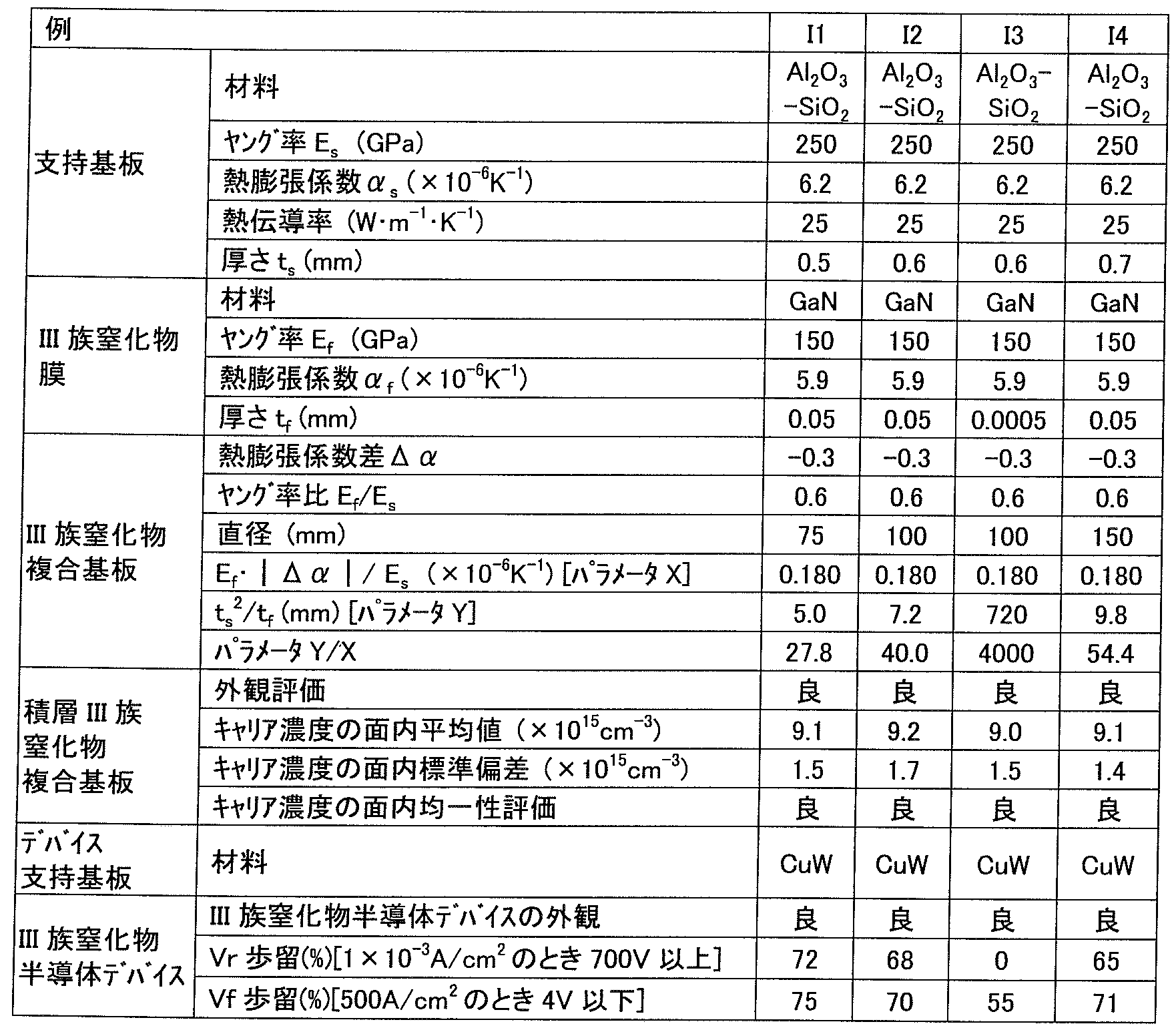
表9を参照して、例I1、例I2および例I4に示すように、支持基板の厚さがそれぞれ0.5mm、0.6mmおよび0.7mmであるIII族窒化物複合基板を用いて作製したIII族窒化物半導体デバイスは、III族窒化物層のキャリア濃度の面内均一性が良でありVf歩留およびVr歩留が高かった。
また、例I3に示すように、III族窒化物膜の厚さが0.0005mmと極めて小さいIII族窒化物複合基板を用いて作製したIII族窒化物半導体デバイスは、III族窒化物層のキャリア濃度の面内均一性が良であったが、Vf歩留およびVr歩留が低くなった。これは、例I3のIII族窒化物半導体デバイスのIII族窒化物膜は、水素イオンの注入により、結晶品質が低下したとともに高抵抗層が形成されたためと考えられた。また、結晶品質が低下したIII族窒化物膜上にエピタキシャル成長させたIII族窒化物層の結晶品質が低下したためと考えられた。
(実施例J)
本実施例は、図17を参照して、支持基板11を含むIII族窒化物半導体デバイス4であるPNDを作製した実施例である。
本実施例は、図17を参照して、支持基板11を含むIII族窒化物半導体デバイス4であるPNDを作製した実施例である。
1.III族窒化物複合基板の作製
支持基板としてMo基板を用いて、支持基板の厚さおよびIII族窒化物膜の厚さが表10の例J1~例J4に示すように異なる直径75mmのIII族窒化物複合基板を作製したこと以外は、実施例Eと同様にして、III族窒化物複合基板を作製した。
支持基板としてMo基板を用いて、支持基板の厚さおよびIII族窒化物膜の厚さが表10の例J1~例J4に示すように異なる直径75mmのIII族窒化物複合基板を作製したこと以外は、実施例Eと同様にして、III族窒化物複合基板を作製した。
また、例J5については、図13を参照して、支持基板11として上記Mo基板を用いて、実施例Hの例H5と同様にして、III族窒化物膜13の厚さが0.0005mmのIII族窒化物複合基板1を作製した。
2.III族窒化物半導体デバイスの作製
図17(A)を参照して、III族窒化物複合基板1のIII族窒化物膜13上に、実施例Iと同様にして、III族窒化物層20として、キャリアストップ層であるキャリア濃度が2×1018cm-3で厚さが1μmのn+-GaN層203、n型キャリアドリフト層であるキャリア濃度が1×1016cm-3で厚さが5μmのn--GaN層204、p型層であるMg濃度が5×1017cm-3で厚さが0.5μmのp--GaN層205、およびオーミックコンタクト層であるMg濃度が1×1020cm-3で厚さが0.05μmのp+-GaN層206を順にエピタキシャル成長させることにより、積層III族窒化物複合基板2を得た。
図17(A)を参照して、III族窒化物複合基板1のIII族窒化物膜13上に、実施例Iと同様にして、III族窒化物層20として、キャリアストップ層であるキャリア濃度が2×1018cm-3で厚さが1μmのn+-GaN層203、n型キャリアドリフト層であるキャリア濃度が1×1016cm-3で厚さが5μmのn--GaN層204、p型層であるMg濃度が5×1017cm-3で厚さが0.5μmのp--GaN層205、およびオーミックコンタクト層であるMg濃度が1×1020cm-3で厚さが0.05μmのp+-GaN層206を順にエピタキシャル成長させることにより、積層III族窒化物複合基板2を得た。
次に、図17(B)を参照して、積層III族窒化物複合基板2のIII族窒化物層20に、実施例Iと同様にして、メサエッチングを行った。メサ部の上底面のサイズは1.4mm角とし、メサ部の高さ(エッチング深さ)は0.8μmとした。次いで、実施例Iと同様にして、III族窒化物層20のp+-GaN層206側に、平面形状が1.1mm角で、厚さ50nmのNi層および厚さ100nmのAu層を順次形成することにより、オーミック電極である第1電極30を形成し、合金化熱処理をした。こうして、III族窒化物半導体デバイス4が得られた。
なお、図17(B)において、支持基板11上にはオーミック電極である第2電極50が形成されているが、本実施例において支持基板11として用いられるMo基板はオーミック電極としても機能するため、支持基板11に第2電極50を設けなかった。
得られたIII族窒化物半導体デバイス4を、実施例Gと同様にして、チップ化した。各III族窒化物半導体デバイスの主面上の外周部5mmを除く全面から上記のチップ化により得られるIII族窒化物半導体デバイスの全個数は、直径75mmの基板からは150個であった。
上記のようにして得られたチップ化されたIII族窒化物半導体デバイスについて、実施例Iと同様にして、Vf歩留およびVr歩留を求めた。得られたチップ化されたIII族窒化物半導体デバイスの特性値を表10にまとめた。
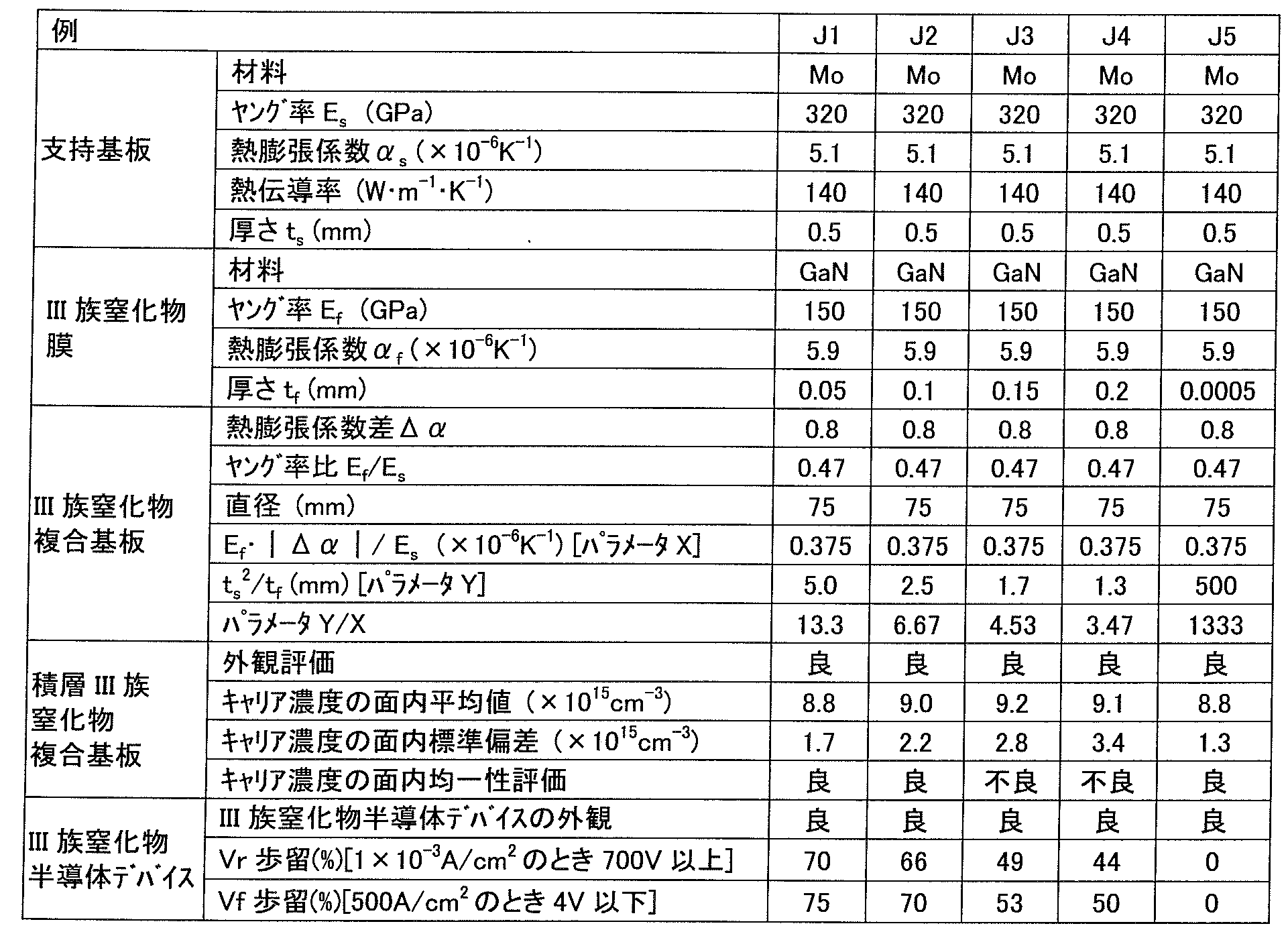
表10を参照して、支持基板としてMo基板を用いたIII族窒化物半導体デバイスにおいては、例J1および例J2に示すように、III族窒化物膜の厚さがそれぞれ0.05mmおよび0.1mmのとき、III族窒化物層のキャリア濃度の面内均一性が良でありVf歩留およびVr歩留が高かったが、例J3および例J4に示すように、III族窒化物膜の厚さがそれぞれ0.15mmおよび0.2mmと大きいとき、III族窒化物層のキャリア濃度の面内均一性が不良でありVf歩留およびVr歩留が低かった。
また、例J5に示すように、III族窒化物膜の厚さが0.0005mmと極めて小さいとき、III族窒化物層のキャリア濃度の面内均一性が良であったが、Vf歩留およびVr歩留が低くなった。これは、例J5のIII族窒化物半導体デバイスのIII族窒化物膜は、水素イオンの注入により、結晶品質が低下したとともに高抵抗層が形成されたためと考えられた。また、結晶品質が低下したIII族窒化物膜上にエピタキシャル成長させたIII族窒化物層の結晶品質が低下したためと考えられた。
今回開示された実施形態および実施例はすべての点で例示であって制限的なものではないと考えられるべきである。本発明の範囲は、上記した説明でなくて請求の範囲によって示され、請求の範囲と均等の意味および範囲内のすべての変更が含まれることが意図される。
1 III族窒化物複合基板、1L,1LS 接合基板、2 積層III族窒化物複合基板、2E 電極付積層III族窒化物複合基板、3 積層基板、4 III族窒化物半導体デバイス、11 支持基板、12,12a,12b,14 接合膜、13 III族窒化物膜、13D,13Dr III族窒化物膜ドナー基板、13i イオン注入領域、15 III族窒化物膜ドナー基板支持体、16D,16Dr 支持体付III族窒化物膜ドナー基板、20 III族窒化物層、30 第1電極、40 デバイス支持基板、43 パッド電極、44 接合金属膜、45 デバイス支持基板電極、50 第2電極、201,203 n+-GaN層、202,204 n--GaN層、205 p--GaN層、206 p+-GaN層、300 絶縁膜、330 バリア膜。
Claims (9)
- 厚さtSが0.1mm以上1mm以下の支持基板と、前記厚さtsに比べて薄い厚さtf
が0.01mm以上0.25mm以下のIII族窒化物膜と、が貼り合わされた直径が75mm以上のIII族窒化物複合基板であって、
前記III族窒化物膜の熱膨張係数αfから前記支持基板の熱膨張係数αsを引いた熱膨張係数差Δαの絶対値|Δα|が2.2×10⁻⁶K-1以下であり、
前記支持基板のヤング率Esおよび前記厚さts、前記III族窒化物膜のヤング率Ef
および前記厚さtf、および前記熱膨張係数差Δαが、次の式(1)
ts 2/tf≧6Ef・|Δα|/Es (1)
の関係を満たすIII族窒化物複合基板。 - 請求項1に記載のIII族窒化物複合基板と、前記III族窒化物複合基板の前記III族窒化物膜上に配置されている少なくとも1層のIII族窒化物層と、を含む積層III族窒化物複合基板。
- 請求項2に記載の積層III族窒化物複合基板中の少なくとも1層の前記III族窒化物層を含むIII族窒化物半導体デバイス。
- 請求項1に記載のIII族窒化物複合基板中の前記III族窒化物膜と、前記III族窒化物膜上に配置された少なくとも1層のIII族窒化物層と、を含むIII族窒化物半導体デバイス。
- 前記支持基板およびデバイス支持基板の少なくともひとつをさらに含む請求項3または請求項4に記載のIII族窒化物半導体デバイス。
- 請求項1に記載のIII族窒化物複合基板の製造方法であって、
支持基板と、III族窒化物膜ドナー基板と、を貼り合わせることにより、直径が75mm以上の接合基板を形成する工程と、
前記接合基板の前記III族窒化物膜ドナー基板の貼り合わせ主面から内部に所定の距離に位置する面で前記III族窒化物膜ドナー基板を切断することにより、前記III族窒化物複合基板を形成する工程と、を含むIII族窒化物複合基板の製造方法。 - 請求項1に記載のIII族窒化物複合基板の製造方法であって、
支持基板と、III族窒化物膜ドナー基板と、を貼り合わせることにより、直径が75mm以上の接合基板を形成する工程と、
前記接合基板の前記III族窒化物膜ドナー基板の貼り合わせ主面と反対側の主面から研削、研磨およびエッチングの少なくともいずれかを行なうことにより、前記III族窒化物複合基板を形成する工程と、を含むIII族窒化物複合基板の製造方法。 - 請求項1に記載のIII族窒化物複合基板を準備する工程と、
前記III族窒化物複合基板の前記III族窒化物膜上に、少なくとも1層のIII族窒化物層を成長させる工程と、を含むIII族窒化物半導体デバイスの製造方法。 - 前記III族窒化物層上にさらにデバイス支持基板を貼り合わせる工程と、前記III族窒化物複合基板から前記支持基板を除去する工程と、をさらに含む請求項8に記載のIII族窒化物半導体デバイスの製造方法。
Priority Applications (2)
| Application Number | Priority Date | Filing Date | Title |
|---|---|---|---|
| US14/433,237 US9312340B2 (en) | 2013-11-13 | 2014-09-04 | Group III nitride composite substrate and method for manufacturing the same, laminated group III nitride composite substrate, and group III nitride semiconductor device and method for manufacturing the same |
| CN201480002997.2A CN104781907B (zh) | 2013-11-13 | 2014-09-04 | Iii族氮化物复合衬底及其制造方法、层叠的iii族氮化物复合衬底、iii族氮化物半导体器件及其制造方法 |
Applications Claiming Priority (2)
| Application Number | Priority Date | Filing Date | Title |
|---|---|---|---|
| JP2013-234993 | 2013-11-13 | ||
| JP2013234993A JP6176069B2 (ja) | 2013-11-13 | 2013-11-13 | Iii族窒化物複合基板およびその製造方法、積層iii族窒化物複合基板、ならびにiii族窒化物半導体デバイスおよびその製造方法 |
Publications (1)
| Publication Number | Publication Date |
|---|---|
| WO2015072214A1 true WO2015072214A1 (ja) | 2015-05-21 |
Family
ID=53057160
Family Applications (1)
| Application Number | Title | Priority Date | Filing Date |
|---|---|---|---|
| PCT/JP2014/073291 Ceased WO2015072214A1 (ja) | 2013-11-13 | 2014-09-04 | Iii族窒化物複合基板およびその製造方法、積層iii族窒化物複合基板、ならびにiii族窒化物半導体デバイスおよびその製造方法 |
Country Status (4)
| Country | Link |
|---|---|
| US (1) | US9312340B2 (ja) |
| JP (1) | JP6176069B2 (ja) |
| CN (1) | CN104781907B (ja) |
| WO (1) | WO2015072214A1 (ja) |
Cited By (3)
| Publication number | Priority date | Publication date | Assignee | Title |
|---|---|---|---|---|
| JPWO2017082197A1 (ja) * | 2015-11-09 | 2018-08-30 | 住友電気工業株式会社 | 下地基板及びiii−v族化合物半導体貼り合せ基板 |
| JP2019523994A (ja) * | 2016-06-14 | 2019-08-29 | クロミス,インコーポレイテッド | 電力およびrf用途用の設計された基板構造 |
| US11387101B2 (en) | 2016-06-14 | 2022-07-12 | QROMIS, Inc. | Methods of manufacturing engineered substrate structures for power and RF applications |
Families Citing this family (8)
| Publication number | Priority date | Publication date | Assignee | Title |
|---|---|---|---|---|
| CN108281378B (zh) * | 2012-10-12 | 2022-06-24 | 住友电气工业株式会社 | Iii族氮化物复合衬底、半导体器件及它们的制造方法 |
| US9859458B2 (en) | 2015-06-19 | 2018-01-02 | QMAT, Inc. | Bond and release layer transfer process |
| US20180019169A1 (en) * | 2016-07-12 | 2018-01-18 | QMAT, Inc. | Backing substrate stabilizing donor substrate for implant or reclamation |
| DE102016015056A1 (de) * | 2016-12-17 | 2018-06-21 | 3-5 Power Electronics GmbH | Herstellungsverfahren eines Schichtstapels aus einem p+-Substrat, einer p--Schicht, einer n--Schicht und einer dritten Schicht |
| JP7391326B2 (ja) * | 2019-12-26 | 2023-12-05 | 株式会社ノベルクリスタルテクノロジー | 半導体装置 |
| WO2021250991A1 (ja) * | 2020-06-09 | 2021-12-16 | 信越化学工業株式会社 | Iii族窒化物系エピタキシャル成長用基板とその製造方法 |
| CN112530855B (zh) * | 2020-12-04 | 2024-04-12 | 中国科学院上海微系统与信息技术研究所 | 复合异质集成半导体结构、半导体器件及制备方法 |
| US20240047203A1 (en) * | 2022-08-04 | 2024-02-08 | Future Semiconductor Business, Inc | Monolithic remote epitaxy of compound semi conductors and 2d materials |
Citations (2)
| Publication number | Priority date | Publication date | Assignee | Title |
|---|---|---|---|---|
| JP2002134422A (ja) * | 2000-10-25 | 2002-05-10 | Matsushita Electric Ind Co Ltd | 窒化物半導体膜の製造方法および窒化物半導体基板の製造方法 |
| JP2013191861A (ja) * | 2013-04-25 | 2013-09-26 | Sumitomo Electric Ind Ltd | 半導体デバイス及びその製造方法 |
Family Cites Families (16)
| Publication number | Priority date | Publication date | Assignee | Title |
|---|---|---|---|---|
| US5248853A (en) * | 1991-11-14 | 1993-09-28 | Nippondenso Co., Ltd. | Semiconductor element-mounting printed board |
| JP3318498B2 (ja) * | 1996-12-27 | 2002-08-26 | 京セラ株式会社 | 半導体素子実装用回路基板 |
| US7380318B2 (en) * | 2003-11-13 | 2008-06-03 | Canon Kabushiki Kaisha | Method of manufacturing liquid discharge head |
| US7253504B1 (en) * | 2004-12-13 | 2007-08-07 | Advanced Micro Devices, Inc. | Integrated circuit package and method |
| JP5003033B2 (ja) | 2006-06-30 | 2012-08-15 | 住友電気工業株式会社 | GaN薄膜貼り合わせ基板およびその製造方法、ならびにGaN系半導体デバイスおよびその製造方法 |
| FR2910179B1 (fr) * | 2006-12-19 | 2009-03-13 | Commissariat Energie Atomique | PROCEDE DE FABRICATION DE COUCHES MINCES DE GaN PAR IMPLANTATION ET RECYCLAGE D'UN SUBSTRAT DE DEPART |
| JP4458116B2 (ja) * | 2007-05-30 | 2010-04-28 | 住友電気工業株式会社 | エピタキシャル層成長用iii族窒化物半導体層貼り合わせ基板および半導体デバイス |
| JP5018423B2 (ja) | 2007-11-20 | 2012-09-05 | 住友電気工業株式会社 | Iii族窒化物半導体結晶基板および半導体デバイス |
| JP5407385B2 (ja) | 2009-02-06 | 2014-02-05 | 住友電気工業株式会社 | 複合基板、エピタキシャル基板、半導体デバイス及び複合基板の製造方法 |
| WO2011132654A1 (ja) * | 2010-04-20 | 2011-10-27 | 住友電気工業株式会社 | 複合基板の製造方法 |
| JP2012069926A (ja) * | 2010-08-21 | 2012-04-05 | Ibiden Co Ltd | プリント配線板及びプリント配線板の製造方法 |
| US8912017B2 (en) * | 2011-05-10 | 2014-12-16 | Ostendo Technologies, Inc. | Semiconductor wafer bonding incorporating electrical and optical interconnects |
| US8796054B2 (en) * | 2012-05-31 | 2014-08-05 | Corning Incorporated | Gallium nitride to silicon direct wafer bonding |
| EP2946410A4 (en) * | 2013-01-16 | 2016-08-03 | Qmat Inc | METHOD FOR PRODUCING OPTOELECTRONIC DEVICES |
| US9368939B2 (en) * | 2013-10-18 | 2016-06-14 | Soraa Laser Diode, Inc. | Manufacturable laser diode formed on C-plane gallium and nitrogen material |
| US9520697B2 (en) * | 2014-02-10 | 2016-12-13 | Soraa Laser Diode, Inc. | Manufacturable multi-emitter laser diode |
-
2013
- 2013-11-13 JP JP2013234993A patent/JP6176069B2/ja not_active Expired - Fee Related
-
2014
- 2014-09-04 CN CN201480002997.2A patent/CN104781907B/zh not_active Expired - Fee Related
- 2014-09-04 WO PCT/JP2014/073291 patent/WO2015072214A1/ja not_active Ceased
- 2014-09-04 US US14/433,237 patent/US9312340B2/en not_active Expired - Fee Related
Patent Citations (2)
| Publication number | Priority date | Publication date | Assignee | Title |
|---|---|---|---|---|
| JP2002134422A (ja) * | 2000-10-25 | 2002-05-10 | Matsushita Electric Ind Co Ltd | 窒化物半導体膜の製造方法および窒化物半導体基板の製造方法 |
| JP2013191861A (ja) * | 2013-04-25 | 2013-09-26 | Sumitomo Electric Ind Ltd | 半導体デバイス及びその製造方法 |
Cited By (5)
| Publication number | Priority date | Publication date | Assignee | Title |
|---|---|---|---|---|
| JPWO2017082197A1 (ja) * | 2015-11-09 | 2018-08-30 | 住友電気工業株式会社 | 下地基板及びiii−v族化合物半導体貼り合せ基板 |
| JP2019523994A (ja) * | 2016-06-14 | 2019-08-29 | クロミス,インコーポレイテッド | 電力およびrf用途用の設計された基板構造 |
| US11387101B2 (en) | 2016-06-14 | 2022-07-12 | QROMIS, Inc. | Methods of manufacturing engineered substrate structures for power and RF applications |
| US12009205B2 (en) | 2016-06-14 | 2024-06-11 | QROMIS, Inc. | Engineered substrate structures for power and RF applications |
| US12217957B2 (en) | 2016-06-14 | 2025-02-04 | QROMIS, Inc. | Engineered substrate structures for power and RF applications |
Also Published As
| Publication number | Publication date |
|---|---|
| CN104781907B (zh) | 2016-11-23 |
| JP6176069B2 (ja) | 2017-08-09 |
| JP2015095589A (ja) | 2015-05-18 |
| US20150349063A1 (en) | 2015-12-03 |
| CN104781907A (zh) | 2015-07-15 |
| US9312340B2 (en) | 2016-04-12 |
Similar Documents
| Publication | Publication Date | Title |
|---|---|---|
| JP6176069B2 (ja) | Iii族窒化物複合基板およびその製造方法、積層iii族窒化物複合基板、ならびにiii族窒化物半導体デバイスおよびその製造方法 | |
| US11094537B2 (en) | Group III nitride composite substrate and method for manufacturing the same, and method for manufacturing group III nitride semiconductor device | |
| US9136337B2 (en) | Group III nitride composite substrate and method for manufacturing the same, laminated group III nitride composite substrate, and group III nitride semiconductor device and method for manufacturing the same | |
| JP6135441B2 (ja) | Iii族窒化物複合基板およびその製造方法、積層iii族窒化物複合基板、ならびにiii族窒化物半導体デバイスおよびその製造方法 | |
| TWI600178B (zh) | III -nitride composite substrate, a method of manufacturing the same, a laminated III-nitride compound substrate, a group III nitride semiconductor device, and a method of fabricating the same | |
| JP4458116B2 (ja) | エピタキシャル層成長用iii族窒化物半導体層貼り合わせ基板および半導体デバイス | |
| JP6772711B2 (ja) | 半導体積層構造体および半導体デバイス | |
| EP3349237A1 (en) | METHOD FOR MANUFACTURING SiC COMPOSITE SUBSTRATE, AND METHOD FOR MANUFACTURING SEMICONDUCTOR SUBSTRATE | |
| CN108140541B (zh) | SiC复合基板的制造方法 | |
| JP6146042B2 (ja) | Iii族窒化物複合基板およびその製造方法、積層iii族窒化物複合基板、ならびにiii族窒化物半導体デバイスおよびその製造方法 | |
| WO2015053127A1 (ja) | Iii族窒化物複合基板およびその製造方法、積層iii族窒化物複合基板、ならびにiii族窒化物半導体デバイスおよびその製造方法 | |
| JP6248395B2 (ja) | Iii族窒化物複合基板およびその製造方法、積層iii族窒化物複合基板、ならびにiii族窒化物半導体デバイスおよびその製造方法 | |
| JP2014157983A (ja) | Iii族窒化物複合基板およびその製造方法、積層iii族窒化物複合基板、ならびにiii族窒化物半導体デバイスおよびその製造方法 | |
| JP2014157979A (ja) | Iii族窒化物複合基板およびその製造方法、積層iii族窒化物複合基板、ならびにiii族窒化物半導体デバイスおよびその製造方法 | |
| JP6146041B2 (ja) | Iii族窒化物複合基板および積層iii族窒化物複合基板、ならびにiii族窒化物半導体デバイスおよびその製造方法 | |
| JP2016149444A (ja) | 窒化ガリウム複合基板およびその製造方法 |
Legal Events
| Date | Code | Title | Description |
|---|---|---|---|
| WWE | Wipo information: entry into national phase |
Ref document number: 14433237 Country of ref document: US |
|
| 121 | Ep: the epo has been informed by wipo that ep was designated in this application |
Ref document number: 14862267 Country of ref document: EP Kind code of ref document: A1 |
|
| NENP | Non-entry into the national phase |
Ref country code: DE |
|
| 122 | Ep: pct application non-entry in european phase |
Ref document number: 14862267 Country of ref document: EP Kind code of ref document: A1 |