WO2015053095A1 - 光走査装置及び画像形成装置 - Google Patents
光走査装置及び画像形成装置 Download PDFInfo
- Publication number
- WO2015053095A1 WO2015053095A1 PCT/JP2014/075589 JP2014075589W WO2015053095A1 WO 2015053095 A1 WO2015053095 A1 WO 2015053095A1 JP 2014075589 W JP2014075589 W JP 2014075589W WO 2015053095 A1 WO2015053095 A1 WO 2015053095A1
- Authority
- WO
- WIPO (PCT)
- Prior art keywords
- cover
- optical
- light beam
- polygon mirror
- light
- Prior art date
- Legal status (The legal status is an assumption and is not a legal conclusion. Google has not performed a legal analysis and makes no representation as to the accuracy of the status listed.)
- Ceased
Links
Images

Classifications
-
- G—PHYSICS
- G03—PHOTOGRAPHY; CINEMATOGRAPHY; ANALOGOUS TECHNIQUES USING WAVES OTHER THAN OPTICAL WAVES; ELECTROGRAPHY; HOLOGRAPHY
- G03G—ELECTROGRAPHY; ELECTROPHOTOGRAPHY; MAGNETOGRAPHY
- G03G15/00—Apparatus for electrographic processes using a charge pattern
- G03G15/04—Apparatus for electrographic processes using a charge pattern for exposing, i.e. imagewise exposure by optically projecting the original image on a photoconductive recording material
- G03G15/043—Apparatus for electrographic processes using a charge pattern for exposing, i.e. imagewise exposure by optically projecting the original image on a photoconductive recording material with means for controlling illumination or exposure
-
- G—PHYSICS
- G02—OPTICS
- G02B—OPTICAL ELEMENTS, SYSTEMS OR APPARATUS
- G02B26/00—Optical devices or arrangements for the control of light using movable or deformable optical elements
- G02B26/08—Optical devices or arrangements for the control of light using movable or deformable optical elements for controlling the direction of light
- G02B26/10—Scanning systems
- G02B26/12—Scanning systems using multifaceted mirrors
-
- H—ELECTRICITY
- H04—ELECTRIC COMMUNICATION TECHNIQUE
- H04N—PICTORIAL COMMUNICATION, e.g. TELEVISION
- H04N1/00—Scanning, transmission or reproduction of documents or the like, e.g. facsimile transmission; Details thereof
- H04N1/04—Scanning arrangements, i.e. arrangements for the displacement of active reading or reproducing elements relative to the original or reproducing medium, or vice versa
- H04N1/06—Scanning arrangements, i.e. arrangements for the displacement of active reading or reproducing elements relative to the original or reproducing medium, or vice versa using cylindrical picture-bearing surfaces, i.e. scanning a main-scanning line substantially perpendicular to the axis and lying in a curved cylindrical surface
-
- H—ELECTRICITY
- H04—ELECTRIC COMMUNICATION TECHNIQUE
- H04N—PICTORIAL COMMUNICATION, e.g. TELEVISION
- H04N1/00—Scanning, transmission or reproduction of documents or the like, e.g. facsimile transmission; Details thereof
- H04N1/04—Scanning arrangements, i.e. arrangements for the displacement of active reading or reproducing elements relative to the original or reproducing medium, or vice versa
- H04N1/113—Scanning arrangements, i.e. arrangements for the displacement of active reading or reproducing elements relative to the original or reproducing medium, or vice versa using oscillating or rotating mirrors
-
- H—ELECTRICITY
- H04—ELECTRIC COMMUNICATION TECHNIQUE
- H04N—PICTORIAL COMMUNICATION, e.g. TELEVISION
- H04N2201/00—Indexing scheme relating to scanning, transmission or reproduction of documents or the like, and to details thereof
- H04N2201/0077—Types of the still picture apparatus
- H04N2201/0082—Image hardcopy reproducer
Definitions
- the present invention relates to an optical scanning device mounted on an electrophotographic image forming apparatus such as a copying machine, a printer, and a facsimile, and an image forming apparatus mounting the optical scanning device.
- An electrophotographic image forming apparatus such as a laser beam printer or a digital copying machine is provided with an optical scanning device for exposing a photosensitive member.
- the light scanning device scans a photosensitive member by deflecting a light beam emitted from a semiconductor laser by a rotating polygon mirror that rotates the light beam.
- an electrostatic latent image is formed on the photosensitive member, and toner is attached to the electrostatic latent image and developed to form a toner image, which is transferred to a sheet to form an image.
- the rotary polygon mirror may be rotated at high speed as one means.
- a high negative pressure is generated inside the light scanning device centering on the vicinity of the rotary polygon mirror, and air can be easily sucked from the outside of the light scanning device.
- the air outside the optical scanning device may be mixed with very fine dust and dirt, and grease volatiles used in the image forming apparatus itself. When such air penetrates the inside of the optical scanning device, adhesion to the reflecting surface of the rotating polygon mirror progresses in several weeks to several months, and the light quantity of exposure decreases, and an image such as an extremely thin density partially appears May cause failure.
- the cover of the optical box is provided with a seal member having elasticity made of synthetic rubber, polyurethane or the like at a joint portion in contact with the outer peripheral edge of the optical box.
- a seal member having elasticity made of synthetic rubber, polyurethane or the like at a joint portion in contact with the outer peripheral edge of the optical box.
- Patent Document 1 for example, the assembling process is performed by forming the seal member made of elastomer integrally with the optical box or the cover instead of attaching the seal member of a separate part.
- the assembling process is performed by forming the seal member made of elastomer integrally with the optical box or the cover instead of attaching the seal member of a separate part.
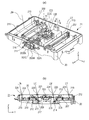
- FIG. 7A is a perspective view showing the appearance of the light scanning device 21 described later.
- the optical scanning device 21 includes an optical box 20 and a cover 30 which covers the open surface of the optical box.
- the optical box 20 integrally holds therein a rotating polygon mirror, various lenses, a folding mirror, and the like, which will be described later.
- the cover 30 covers the open surface of the optical box 20 and seals the inside of the optical box 20. The details of the light scanning device 21 will be described later.
- the cover 30 has a seal portion formed by injection molding in order to ensure the airtightness inside the optical box 20.
- the gate portion 31a for filling the melting material forming the seal portion is required.
- the injection molding is performed so as to protrude from the gate portion 31a.
- the runner portion 31c in the shape of the injection nozzle of the machine remains. Therefore, depending on the position where the gate portion 31a is provided, as shown in FIG.
- the runner portion 31c blocks the optical path of the synchronous light incident on the synchronous sensor, causing malfunction of the optical scanning device or the photosensitive member. There is a concern that an image defect may occur. In addition, when the runner portion 31c contacts the folding mirror or the lens, the lens or the like is pushed away and shifted, and there is a concern that the irradiation position of the light beam to the photosensitive body is largely shifted. As a result, in order to prevent this, there has been a problem that an extra work process such as cutting the runner portion 31c protruding from the gate portion 31a is required.
- the present invention has been made under such circumstances, and it is an object of the present invention to injection-mold a seal portion with a simple configuration that does not require complicated assembly operations.
- the present invention is configured as follows.
- An optical scanning device comprising: an optical member for guiding light to the photosensitive member; an optical box for accommodating the light source, the rotary polygon mirror, and the optical member; and a cover for covering an opening of the optical box A dustproof member sandwiched between the cover and the side wall of the optical box and molded on the cover to dustproof the inside of the optical box, a gate unit for injecting the melted dustproof member, and the gate unit A flow path through which the melted dust-proof member injected from the side flows, and by attaching the cover to the optical box, the dust-proof member is sandwiched between the side wall and the cover. It has a channel formed on over the said gate portion includes an optical scanning device, characterized in that provided as viewed from a direction of a rotation axis of the rotary
- An optical scanning device comprising: an optical member for guiding light to the photosensitive member; an optical box for accommodating the light source, the rotary polygon mirror, and the optical member; and a cover for covering an opening of the optical box A dustproof member sandwiched between the cover and the side wall of the optical box and molded on the cover to dustproof the inside of the optical box, a gate unit for injecting the melted dustproof member, and the gate unit A flow path through which the melted dust-proof member injected from the side flows, and by attaching the cover to the optical box, the dust-proof member is sandwiched between the side wall and the cover.
- the gate portion is located at a position where the virtual normal extending from the gate portion to the cover does not intersect the optical path region of the light beam in the optical box
- An optical scanning device comprising: an optical member for guiding light to the photosensitive member; an optical box for containing the light source, the rotary polygon mirror, and the optical member; and a cover for covering the opening of the optical box
- the box has a wall standing from the bottom so as to surround the rotary polygon mirror installed at the bottom of the optical box, the cover is an opening surrounded by the wall, and the rotary polygon mirror
- the first cover comprising A dustproof member sandwiched between the first cover and the erected wall and formed on the first cover to dustproof the inside of the optical box, and
- An optical scanning device comprising: an optical member for guiding light to the photosensitive member; an optical box for containing the light source, the rotary polygon mirror, and the optical member; and a cover for covering the opening of the optical box
- the box has a wall standing from the bottom so as to surround the rotary polygon mirror installed at the bottom of the optical box, the cover is an opening surrounded by the wall, and the rotary polygon mirror A first cover covering a first opening through which the rotary polygon mirror passes when the light source is installed at the bottom, and a second cover covering a second opening which is the opening of the optical box excluding the first opening A cover, the first cover comprising A dustproof member sandwiched between the first cover and the erected wall and formed on the first cover to dustproof the inside of the optical box,
- the seal portion can be injection-molded with a simple configuration that does not require a complicated assembly operation.
- Schematic cross-sectional view of the image forming apparatus of Example 1 The perspective view which shows the structure of the optical scanning device of Example 1, 2, and sectional drawing of an optical scanning device The figure explaining the cover composition of Example 1, a gate part The figure which explains the gate section arrangement territory of execution example 1
- Schematic cross-sectional view of the image forming apparatus of Example 2 The perspective view which shows the structure of the optical scanning device of Example 2, the figure explaining a cover structure, and a gate part
- the rotational axis direction of the rotary polygon mirror 203 described later is the Z axis direction
- the main scanning direction which is the scanning direction of the light beam or the longitudinal direction of the reflecting mirror is perpendicular to the X axis direction
- X axis and Z axis Direction is taken as the Y-axis direction.
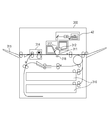
- FIG. 1 is a schematic cross-sectional view of an electrophotographic image forming apparatus 100 according to the first embodiment.
- the image forming apparatus 100 illustrated in FIG. 1 includes four image forming units 101Y, 101M, 101C, and 101Bk that form toner images of yellow (Y), magenta (M), cyan (C), and black (Bk), respectively. Equipped with Hereinafter, the symbols Y, M, C, and Bk representing the respective colors are omitted unless necessary.
- the image forming unit 101 includes photosensitive drums 102 which are photosensitive members.
- Each image forming unit also includes a charging device 103 for charging the photosensitive drum 102 and a developing device 104 for developing the electrostatic latent image on the photosensitive drum with toner. Furthermore, each image forming unit includes a cleaning device 111 that removes the toner remaining on the photosensitive drum from the photosensitive drum (on the photosensitive member).
- Each image forming unit constitutes a process cartridge in which the photosensitive drum 102, the charging device 103, the developing device 104, and the cleaning device 111 described above are integrated.
- the process cartridge is a replaceable unit that can be attached to and detached from the image forming apparatus 100.
- the image forming units 101Y, 101M, 101C, and 101Bk will be referred to as process cartridges 101Y, 101M, 101C, and 101Bk.
- the main body of the image forming apparatus 100 is provided with an optical scanning device 21, transfer rollers 105 Y, 105 M, 105 C, 105 Bk, an intermediate transfer belt 106, a paper feed unit 109, a paper discharge unit 110, a transfer roller 107, and a fixing device 108.
- the intermediate transfer belt 106 rotates in the arrow direction (counterclockwise direction) in the drawing.
- the optical scanning device 21 is disposed below the photosensitive drums 102 in the direction of gravity (in the direction of the ⁇ Z axis).
- the optical scanning device 21 may be arranged to expose the photosensitive drum 102 from the upper side in the direction of gravity (the + Z-axis direction).
- the light scanning device 21 emits light beams LY, LM, LC, and LBk for exposing the photosensitive drums 102Y, 102M, 102C, and 102Bk charged by the charging devices 103Y, 103M, 103C, and 103Bk, respectively.
- electrostatic latent images are formed on the photosensitive drums 102Y, 102M, 102C, and 102Bk.
- the developing device 104 ⁇ / b> Y develops the electrostatic latent image formed on the photosensitive drum 102 ⁇ / b> Y with yellow toner.
- the developing device 104M develops the electrostatic latent image formed on the photosensitive drum 102M with magenta toner.
- the developing device 104C develops the electrostatic latent image formed on the photosensitive drum 102C with cyan toner.
- the developing device 104Bk develops the electrostatic latent image formed on the photosensitive drum 102Bk with black toner.
- the yellow toner image formed on the photosensitive drum 102Y is transferred to the intermediate transfer belt 106, which is an intermediate transfer member, by the transfer roller 105Y at the transfer portion Ty.
- the cleaning device 111Y collects the toner remaining on the photosensitive drum 102Y without being transferred to the intermediate transfer belt 106 between the transfer portion Ty in the rotational direction of the photosensitive drum 102Y and the charging portion of the charging device 103Y.
- the magenta toner image formed on the photosensitive drum 102M is transferred to the intermediate transfer belt 106 by the transfer roller 105M at the transfer portion Tm.
- the cleaning device 111M collects toner remaining on the photosensitive drum 102M without being transferred to the intermediate transfer belt 106 between the transfer portion Tm in the rotational direction of the photosensitive drum 102M and the charging portion of the charging device 103M.
- the cyan toner image formed on the photosensitive drum 102C is transferred to the intermediate transfer belt 106 by the transfer roller 105C at the transfer portion Tc.
- the cleaning device 111C collects the toner remaining on the photosensitive drum 102C without being transferred to the intermediate transfer belt 106 between the transfer portion Tc in the rotational direction of the photosensitive drum 102C and the charging portion of the charging device 103C.
- the black toner image formed on the photosensitive drum 102Bk is transferred to the intermediate transfer belt 106 by the transfer roller 105Bk at the transfer portion TBk.
- the cleaning device 111Bk collects the toner remaining on the photosensitive drum 102Bk without being transferred to the intermediate transfer belt 106 between the transfer portion TBk in the rotational direction of the photosensitive drum 102Bk and the charging portion of the charging device 103Bk.
- the cleaning device 111 of the present embodiment is provided with a blade that contacts the photosensitive drum 102, and the residual toner is collected by scraping off the toner remaining on the photosensitive drum by the blade.
- the toner images of the respective colors transferred onto the intermediate transfer belt 106 are transferred by the transfer roller 107 onto the recording sheet conveyed from the sheet feeding unit 109 at the transfer portion T2.
- the toner image transferred onto the recording sheet at the transfer unit T2 is subjected to a fixing process by the fixing device 108, and is discharged to the sheet discharge unit 110 after the fixing process.
- the above-described image forming apparatus 100 forms an image forming apparatus for monochrome image forming apparatus having one photosensitive drum, or directly forms a toner image formed on a plurality of photosensitive drums onto a recording medium. It may be an apparatus.
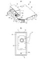
- FIG. 2A is a perspective view showing the configuration of the light scanning device 21, and FIG. 2B is a cross-sectional view of the light scanning device 21.
- light source units 202Y, 202M, 202C, 202Bk are attached to the outer wall of the optical box 20 of the light scanning device 21.
- the light source unit 202Y emits a light beam LY for exposing the photosensitive drum 102Y
- the light source unit 202M emits a light beam LM for exposing the photosensitive drum 102M
- the light source unit 202C emits a light beam LC for exposing the photosensitive drum 102C
- the light source unit 202Bk emits a light beam LBk for exposing the photosensitive drum 102Bk.
- the light source units 202Y, 202M, 202C, 202Bk are arranged close to each other.
- a plane crossing the rotating polygon mirror 203 with the rotation axis of the rotating polygon mirror 203 as a normal is defined as a virtual plane.
- the light beam LY emitted from the light source unit 202Y and the light beam LBk emitted from the light source unit 202Bk have an optical path obliquely incident from the upper side in the direction of gravity (+ Z axis direction) with respect to the virtual plane. It is incident on the reflective surface.
- the light beam LC emitted from the light source unit 202C and the light beam LM emitted from the light source unit 202M have an optical path obliquely incident from the lower side in the direction of gravity (-Z-axis direction) to the virtual plane described above.
- the light is incident on the reflecting surface of the rotating polygon mirror 203.
- a rotary polygon mirror 203 having four reflecting surfaces is provided at the center of the optical box 20. As shown in FIG. At the time of image formation, the rotary polygon mirror 203 rotates the rotation axis shown by the dotted line in FIG. 2A in the R1 direction.
- the light beam LY emitted from the light source unit 202Y is incident on the reflecting surface of the rotating polygon mirror 203.
- the light beam LY is deflected (reflected) to the side A shown in FIG. 2A by the reflecting surface of the rotating polygon mirror 203.
- the light beam LM emitted from the light source unit 202M is incident on the same reflection surface as the reflection surface of the rotary polygon mirror 203 on which the light beam LY is incident.
- the light beam LM is deflected by the reflecting surface of the rotating polygon mirror 203 to the same side (A side) as the light beam LY.
- the light beam LBk emitted from the light source unit 202Bk is incident on a reflection surface different from the reflection surface on which the light beams LY and LM are incident.
- the light beam LBk is deflected to the B side shown in FIG. 2A by the reflecting surface of the rotating polygon mirror 203.
- the light beam LC emitted from the light source unit 202C is incident on the same reflection surface as the reflection surface of the rotary polygon mirror 203 on which the light beam LBk is incident.
- the light beam LC is deflected to the same side (B side) as the light beam LBk by the reflection surface of the rotating polygon mirror 203.
- the light beams LY and LM deflected by the rotary polygon mirror 203 become light beams moving in the + X direction. That is, by being deflected by the rotating polygon mirror 203, the light beam LY becomes a light beam scanning the photosensitive drum 102Y in the + X direction, and the light beam LM becomes a light beam scanning the photosensitive drum 102M in the + X direction.
- the light beams LBk and LC deflected by the rotating polygon mirror 203 become light beams moving in the ⁇ X direction. That is, by being deflected by the rotating polygon mirror 203, the light beam LBk becomes a light beam for scanning the photosensitive drum 102Bk in the -X direction, and the light beam LC is a light beam for scanning the photosensitive drum 102C in the -X direction. Become.
- the optical paths of the light beams LY, LM, LC, and LBk deflected by the rotary polygon mirror 203 will be described with reference to FIG. 2B.
- the optical members of the present invention are accommodated and installed at the bottom (bottom) of the optical box 20.
- a rotary polygon mirror 203, each lens described above, and a cover 30 for dustproofing each reflection mirror are attached to an opening which is an open surface at the top of the optical box 20.
- the light beam LY deflected by the rotary polygon mirror 203 passes through the lens 206 and the lens 207 and then enters the reflection mirror 212.
- the reflection mirror 212 reflects the incident light beam LY toward the photosensitive drum 102Y.
- the cover 30 is formed with an opening 219 through which the light beam LY reflected by the reflection mirror 212 passes.
- the opening 219 is closed by a dustproof window 223 which is a transparent transparent window for passing the light beam LY.
- the light beam LY passing through the dustproof window 223 forms an image on the photosensitive drum 102Y.
- the light beam LM deflected by the rotating polygon mirror 203 passes through the lens 206 and then enters the reflection mirror 213.
- the reflection mirror 213 reflects the incident light beam LM toward the reflection mirror 214.
- the light beam LM reflected by the reflection mirror 213 passes through the lens 208 and enters the reflection mirror 214.
- the reflection mirror 214 reflects the incident light beam LM toward the photosensitive drum 102M.
- the cover 30 is formed with an opening 220 through which the light beam LM reflected by the reflection mirror 214 passes.
- the opening 220 is closed by a transparent dustproof window 224 through which the light beam LM passes.
- the light beam LM passing through the dustproof window 224 forms an image on the photosensitive drum 102M.
- the light beam LBk deflected by the rotating polygon mirror 203 is incident on the reflecting mirror 215 after passing through the lens 209 and the lens 210.
- the reflection mirror 215 reflects the incident light beam LBk toward the photosensitive drum 102Bk.
- the cover 30 is formed with an opening 222 through which the light beam LBk reflected by the reflection mirror 215 passes.
- the opening 222 is closed by a transparent dustproof window 226 which allows the light beam LBk to pass.
- the light beam LBk that has passed through the dustproof window 226 forms an image on the photosensitive drum 102Bk.
- the light beam LC deflected by the rotating polygon mirror 203 passes through the lens 209 and then enters the reflecting mirror 216.
- the reflection mirror 216 reflects the incident light beam LC toward the reflection mirror 217.
- the light beam LC reflected by the reflection mirror 216 passes through the lens 211 and enters the reflection mirror 217.
- the reflection mirror 217 reflects the incident light beam LC toward the photosensitive drum 102C.
- the cover 30 is formed with an opening 221 through which the light beam LC reflected by the reflection mirror 217 passes.
- the opening 221 is closed by a transparent dustproof window 225 through which the light beam LC passes.
- the light beam LC that has passed through the dustproof window 225 forms an image on the photosensitive drum 102C.
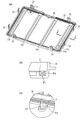
- FIG. 3A is a view showing the configuration of the cover 30 in the present embodiment, and is a perspective view of the cover 30 as viewed from the optical box 20 side.
- the cover 30 is provided with a plurality of hook portions 32 constituting a snap-fit structure by engaging a protrusion provided on the outer wall of the optical box 20.
- dustproof windows 223, 224, 225 and 226 are provided in the cover 30.
- a seal portion 31 which is a dustproof member is formed on the cover 30 by injection molding around the entire circumference that faces the outer peripheral edge formed by the side wall of the optical box 20 when attached to the optical box 20.
- the gate portion 31a for injecting a molten hot melt adhesive (hereinafter referred to as "hot melt") of a polyolefin type which is a molded member is two places in FIG. It is provided at a position that divides the entire length into almost two halves.
- the gate portions 31a are provided in two places in this embodiment, but may be increased or decreased according to the actual formability, and at least one or more places may be provided.
- FIG. 3B is a JJ cross-sectional view of the cover 30 cut at the position of JJ (one-dot chain line) indicated by a white arrow shown in FIG.
- FIG. 6 is a cross-sectional view showing the relationship of a portion 31.
- the cover 30 is provided with a groove 30a through which the melted hot melt injected from the gate 31a flows, and the seal 30 is formed by filling the groove 30a with the hot melt. Be done.
- the groove portion 30 a is formed such that the seal portion 31 is sandwiched between the side wall of the optical box 20 and the cover 30 by attaching the cover 30 to the optical box 20. Furthermore, in the groove 30a, a narrower anchor groove 30c having a smaller width and a smaller depth is provided, and the contact area between the cover 30 and the seal portion 31 is enlarged. Thus, the adhesion between the cover 30 and the seal portion 31 is secured so that the seal member, which is a dustproof member, does not unintentionally peel off from the cover 30. In addition, a concave groove is formed on the surface of the seal portion 31, and the outer peripheral edge formed by the side wall of the optical box 20 is inserted into the groove, thereby dustproofing the inside of the optical box 20 Sealing of 20 is also secured.
- FIG.3 (c) is the figure which expanded the part (gate part 31a peripheral part) of the cover 30 enclosed with the circle in FIG. 3 (a).
- the seal portion 31 is formed by injection molding, hot melt is injected from the gate portion 31a through an injection nozzle. Therefore, as shown in FIG. 3C, after the injection of the hot melt is completed, the molding material remaining in the injection nozzle is solidified as it is, and the runner portion 31c having a nozzle shape is formed in the gate portion 31a. .
- the runner portion 31c blocks the optical path of the light beam in the optical box 20, or the optical unit disposed in the optical box 20. There is a possibility that the position or position of the optical component may be changed by coming into contact with the component.
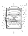
- FIG. 4 is a view of the optical scanning device 21 of this embodiment as viewed from the lower side (-Z-axis direction), except for the optical box 20, and the optical components disposed inside the cover 30 and the optical scanning device 21 It is the figure which showed the lens, the reflective mirror, etc. etc.
- light beams emitted from the light source units 202 pass through the incident light path L1 and enter the rotating polygon mirror (not shown in FIG. 4) driven by the polygon motor 232.
- the light source units 202 disposed on the A side are the light source units 202Y and 202M described above
- the light source units 202 disposed on the B side are the light source units 202C and 202Bk described above.
- the light beam incident on the rotary polygon mirror that rotates in the arrow direction is deflected to the reflection mirrors 212 and 215 along the scanning light path L2 or L3.
- the scanning direction indicates the direction in which the light beam deflected by the rotating polygon mirror is scanned.
- the light beams emitted from the light source units 202Y and 202M are deflected to the side A in the drawing (rightward in the drawing).
- the scanning light path L2 indicates the scanning light path to the reflection mirror 212 of the light beam emitted from the light source unit 202Y.
- the light beams emitted from the light source units 202C and 202Bk are deflected to the side B in the drawing (the left direction in the drawing).
- the scanning light path L3 indicates the scanning light path to the reflection mirror 215 of the light beam emitted from the light source unit 202Bk.
- the scanning light path L2 indicates the light path at the start of scanning of the light beam toward the reflecting mirror 212 and at the end of scanning.
- the scanning light path L3 indicates the light path at the start of scanning of the light beam toward the reflecting mirror 215 and at the end of scanning.
- the light beam emitted from the light source unit 202 is deflected by the rotary polygon mirror (not shown in FIG. 4), and the synchronization sensor 231 is transmitted via the anamorphic lens 230 along the synchronization light path L4. Make it incident.
- the synchronization sensor 231 generates, based on the timing of the incident light beam, a synchronization signal that indicates a scan start timing for irradiating the light beam from the light source unit 202.
- the other reference numerals in FIG. 4 are described in FIG. 2 and thus the description thereof is omitted here.
- optical components (lenses 206 to 211, reflection mirrors 212, 213, 215, 216, etc.), mechanical components for fixing the lenses and mirrors, etc. are installed inside the light scanning device 21.
- electrical components such as a polygon motor 232 and a synchronous sensor 231 are installed inside the light scanning device 21, and in the space inside the light scanning device 21, an incident light path L 1 through which a light beam passes and scanning light paths L 2 and L 3 , Synchronous light path L4.
- the optical paths L1 to L4 are indicated by two solid lines, respectively, and the light beam passes through an optical path region which is a space occupied by the two solid lines.
- the scanning light paths L2 and L3 indicate the largest light paths in the light scanning device 21, which is the space occupied by the scanning light paths.
- a gate portion arrangement region there is a region surrounded by a broken line in which neither a component nor an optical path exists, which is referred to as a “gate portion arrangement region”.
- the gate portion 31a is formed at a position where the virtual normal extending from the gate portion 31a to the cover 30 perpendicularly does not intersect the optical path region of the light beam in the optical box 20. Therefore, when the gate portion 31a is provided in the gate portion arrangement region, the light path is blocked by the runner portion 31c formed in the gate portion 31a, or the runner portion 31c contacts the component to change the posture. There will be no more.
- reflecting mirrors for example, reflecting mirrors 212 and 215
- scanning lenses for example, lenses 207 and 210
- X-axis direction the scanning direction of the scanning optical system.
- a reflection mirror and a scanning lens are arranged in the vicinity of the outer peripheral edge (short side in the figure) of the optical box 20 parallel to the scanning direction (X-axis direction)
- the area in which the gate portion is disposed is an area other than the side parallel to the scanning direction (X-axis direction) of the light scanning device 21, that is, the outer peripheral side (long side) of the side in the direction (Y-axis direction) orthogonal to the scanning direction. It is preferable to provide it on the side).
- the process of affixing a separate seal member on a cover can be eliminated by providing the seal part 31 integrally with the cover 30 by injection molding, and the additional process of cutting the runner part 31c of the seal part 31
- the work process also becomes unnecessary.
- the process of producing the cover with the seal member is simplified, and the cost of parts can be reduced.
- the shape of the seal portion 31 becomes constant, it is possible to stably ensure good sealing.
- each gate in the case of providing a plurality of gate portions 31 a so as to divide the entire flow path substantially equally.
- the seal portion can be injection-molded with a simple configuration that does not require a complicated assembly operation.
- a negative pressure may be generated inside the device by the rotation of the polygon motor, and air outside the optical scanning device may be easily sucked into the device. Therefore, there is also an optical scanning device of a configuration in which the portion on which the polygon motor is mounted in the optical scanning device is an independent space by a partition or the like.
- a gate portion arrangement region of a cover in the case of sealing a space in which a polygon motor is installed with a cover sealed by a seal member will be described.
- FIG. 5 is a view showing a schematic configuration of a laser beam printer 300.
- the laser beam printer 300 is a monochrome image forming apparatus having one photosensitive drum.
- the laser beam printer 300 includes a photosensitive drum 311 on which an electrostatic latent image is formed by the light scanning device 42, a charging device 317 for uniformly charging the photosensitive drum 311, and a toner on the electrostatic latent image formed on the photosensitive drum 311.
- the laser beam printer 300 includes a controller (not shown) that controls an image forming operation by the image forming unit and a conveyance operation of the recording sheet.
- FIG. 6A is a perspective view showing the appearance of the optical scanning device 42 of this embodiment.
- the optical box 33 has a first opening which is an open surface formed by partition walls 43a, 43b, 43c and 43d described later, and a second opening which is an open surface of the optical box excluding the first opening. doing. Then, the optical box 33 is sealed by the cover 34 which is the first opening and the cover 35 which is the second opening.
- C indicates the upper portion of the cover 35
- D indicates the lower portion of the cover 35.
- the space sealed by the cover 35 is a space surrounded by partition walls 43a, 43b, 43c and 43d, which are formed integrally with the optical box 33 in the optical scanning device 42.
- the partition walls 43a, 43b, 43c and 43d are provided to stand from the bottom of the optical box 33, and adjacent partition walls are connected. Further, the partition wall 43a is provided with an opening 39 through which the light beam passes.
- a polygon motor 36 and a rotary polygon mirror 37 rotationally driven by the polygon motor 36 are mounted on the bottom of the optical box 33 surrounded by the partition walls 43a, 43b, 43c and 43d.
- the light beam emitted from the light source unit 38 is reflected by a reflection mirror (not shown) provided inside the light scanning device 42 sealed by the cover 34, and then enters the rotary polygon mirror 37 through the opening 39. (Indicated by a broken arrow in the figure). Then, the light beam that has entered the rotary polygon mirror 37 is deflected, and again enters the side sealed by the cover 34 through the opening 39.
- FIG. 6A a cover 35 is provided which covers only the open surface of the upper part of the independent space in which the polygon motor 36 is mounted on the bottom surface.
- FIG. 6B is a view looking up the cover 35 from the polygon motor 36 side (the bottom side of the optical scanning device 42), so that the positional relationship with the seal portion 40 formed on the outer peripheral edge of the cover 35 can be understood.
- the outer shape of the polygon motor 36 is overlapped.
- the scanning light path L5 (indicated by broken lines) shows the light path of the light beam (reflected light) reflected and deflected by the light beam incident on the rotating polygon mirror 37, and is occupied by two broken lines. A light beam passes through an optical path area which is space.
- the cover 35 has a seal portion 40, a gate portion 40a, and a flow path through which the melted hot melt injected from the gate portion 40a flows.
- the seal portion 40 is a dustproof member which is sandwiched between the cover 35 and the partition walls 43a, 43b, 43c, 43d and is formed on the cover 35 in order to dustproof the inside of the optical box.
- the gate portion 40 a is used to inject a molten hot melt to form the seal portion 40.
- the seal portion 40 is formed so as to be sandwiched between the partition walls 43 a, 43 b, 43 c, 43 d and the cover 35. Be done.
- the seal portion 40 is injection molded on the entire circumference along the edge of the cover 35, and the gate portion 40a for the molding is provided.
- the gate portion 40a is in the optical box 33 surrounded by the imaginary normal line extending perpendicularly to the cover 35 from the gate portion 40a and the partition walls 43a to 43d. It is formed in the position which does not cross with the optical path area
- the seal portion 40 integrally with the cover 35 by injection molding, the step of attaching a separate seal member to the cover can be eliminated, and the step of cutting the runner portion of the seal portion 40 is also performed. It becomes unnecessary. As a result, the process of producing the cover with the seal member is simplified, and the cost of parts can be reduced. Furthermore, as an effect of molding, since the shape of the seal portion 40 becomes constant, good sealing performance can be ensured.
- the cover 34 as in the first embodiment, the optical member installed inside the optical box 33 covered by the cover 34, the incident light path through which the light beam passes, the scanning light path and the synchronous light path The same effect as that of the first embodiment can be obtained by providing. As described above, according to this embodiment, the seal portion can be injection-molded with a simple configuration that does not require a complicated assembly operation.
Landscapes
- Physics & Mathematics (AREA)
- Engineering & Computer Science (AREA)
- Multimedia (AREA)
- Signal Processing (AREA)
- General Physics & Mathematics (AREA)
- Optics & Photonics (AREA)
- Mechanical Optical Scanning Systems (AREA)
- Facsimile Scanning Arrangements (AREA)
- Laser Beam Printer (AREA)
Abstract
煩雑な組立作業を必要としない簡便な構成で、シール部を射出成形すること。 光ビームを出射する光源ユニット202と、光源ユニット202から出射された光ビームが感光体上を走査するように光ビームを偏向する回転多面鏡203と、回転多面鏡203によって偏向された光ビームを感光体に導く光学部材と、光源ユニット202、回転多面鏡203、及び光学部材を収容する光学箱20と、光学箱20の開口を覆うカバー30と、を備える光走査装置21であって、カバー30は、カバー30と光学箱20の側壁とによって挟まれるように成形されたシール部31aと、ホットメルトを注入するためのゲート部31aと、シール部31aが光学箱20の側壁とカバー30とにより挟まれるように形成されるためのホットメルトが流れる流路と、を有し、ゲート部31aは、回転多面鏡203の回転軸方向から見て光ビームの光路領域の外に設けられる。
Description
本発明は、複写機やプリンタ及びファクシミリなどの電子写真方式の画像形成装置に搭載される光走査装置、及びこの光走査装置を搭載した画像形成装置に関する。
レーザビームプリンタやデジタル複写機などの電子写真方式の画像形成装置においては、感光体を露光するための光走査装置が備えられている。光走査装置は、半導体レーザから出射される光ビームを回転する回転多面鏡で偏向して感光体上を走査する。これによって感光体上に静電潜像が形成され、この静電潜像にトナーを付着させて現像することによりトナー像が形成され、これを用紙に転写して画像を形成する。
近年は画像形成装置のカラー化が進展し、カラー画像形成装置においては、それぞれの色ごとに専用の感光体を備えて各色の画像を中間転写体上に一括して形成する、いわゆるタンデム方式と呼ばれる方式が主流になってきている。更に、このタンデム方式の画像形成装置においては、ユニットサイズとコストで有利であることから、1つの回転多面鏡で4色の露光をすべて行う、いわゆる4in1構成の光走査装置が広く用いられている。
ところで、近年の画像形成装置の傾向としては、前述したカラー化に加えて、高速化や高解像度化が挙げられる。この高速化及び高解像度化を実現するためには、1つの手段として回転多面鏡を高速で回転させればよい。しかし、回転多面鏡を高速で回転させると、回転多面鏡付近を中心として光走査装置内部に高い負圧が発生し、光走査装置の外部から空気を吸い込みやすくなる。この光走査装置外部の空気には、ごく微小な塵や埃、及び画像形成装置自体に使用されているグリス類の揮発物が混じっている場合がある。そのような空気が光走査装置内部に侵入すると、数週間から数カ月で回転多面鏡の反射面への付着が進行し、露光の光量が減少して部分的に濃度が極端に薄くなるなどの画像不良を引き起こすことがある。
これを防ぐために、光学箱のカバーには、光学箱の外周縁と当接する接合部に、合成ゴムやポリウレタンなどを材料とする弾性を備えたシール部材が取り付けられており、これをカバーと光学箱で挟み込むことで、光学箱内部の密閉性を確保している。このシール部材は、これまでは独立した部品を両面テープによって、カバー又は光学箱に貼り付けていたが、確実に密閉するためには、カバー部材や光学箱の形状に沿って丁寧に貼り付ける必要があり、その作業は煩雑であった。
これに対して、例えば特許文献1では、別部品のシール部材を貼り付けるのではなく、エラストマ製のシール部材を、光学箱又はカバーに一体的に射出成形する構成とすることにより、組立工程を簡素化しつつ、密閉性を備えた光走査装置を提案している。
図7(a)は、後述する光走査装置21の外観を示した斜視図である。図7(a)に示すように、光走査装置21は、光学箱20と光学箱の開放面を覆うカバー30から構成されている。光学箱20には、後述する回転多面鏡、各種レンズ、折り返しミラー等が内部に一体的に保持されている。そして、カバー30は、光学箱20の開放面を覆って、光学箱20の内部を密閉する。なお、光走査装置21の詳細については、後述する。
カバー30は、光学箱20内部の密閉性を確保するため、射出成形によりシール部が形成されている。光学箱20のカバー30にシール部材を射出成形する場合、シール部を形成する溶解材料を充填するためのゲート部31aが必要となる。そして、ゲート部31aから溶融材料を充填してシール部を射出成形すると、図7(b)に示すように、一般的な射出成形品と同様に、ゲート部31aから突出する形で、射出成形機の射出ノズルの形状をしたランナー部31cが残ってしまう。そのため、ゲート部31aを設ける位置によっては、図7(b)に示すようにランナー部31cが同期センサに入射される同期光の光路を遮ってしまい、光走査装置の動作不良や感光体上に形成される画像不良を起こしたりすることが懸念される。また、ランナー部31cが折り返しミラーやレンズに接触することにより、レンズ等を押しのけてずらしてしまい、感光体への光ビームの照射位置が大きくずれたりすることが懸念される。その結果、これを防ぐためには、ゲート部31aから突出したランナー部31cをカットするなどの余計な作業工程が必要となるという課題があった。
本発明はこのような状況のもとでなされたものであり、煩雑な組立作業を必要としない簡便な構成で、シール部を射出成形することを目的とする。
前述した課題を解決するため、本発明では次のとおりに構成する。
(1)光ビームを出射する光源と、前記光源から出射された光ビームが感光体上を走査するように前記光ビームを偏向する回転多面鏡と、前記回転多面鏡によって偏向された前記光ビームを前記感光体に導く光学部材と、前記光源、前記回転多面鏡、及び前記光学部材を収容する光学箱と、前記光学箱の開口を覆うカバーと、を備える光走査装置であって、前記カバーは、前記カバーと前記光学箱の側壁とによって挟まれ、光学箱内部を防塵するために前記カバーに成形された防塵部材と、溶融した前記防塵部材を注入するためのゲート部と、前記ゲート部から注入された溶融した前記防塵部材が流れる流路であって、前記カバーを前記光学箱に取り付けることによって前記防塵部材が前記側壁と前記カバーとによって挟まれるように前記カバーに形成された流路と、を有し、前記ゲート部は、前記回転多面鏡の回転軸方向から見て前記光ビームの光路領域の外に設けられることを特徴とする光走査装置。
(2)光ビームを出射する光源と、前記光源から出射された光ビームが感光体上を走査するように前記光ビームを偏向する回転多面鏡と、前記回転多面鏡によって偏向された前記光ビームを前記感光体に導く光学部材と、前記光源、前記回転多面鏡、及び前記光学部材を収容する光学箱と、前記光学箱の開口を覆うカバーと、を備える光走査装置であって、前記カバーは、前記カバーと前記光学箱の側壁とによって挟まれ、光学箱内部を防塵するために前記カバーに成形された防塵部材と、溶融した前記防塵部材を注入するためのゲート部と、前記ゲート部から注入された溶融した前記防塵部材が流れる流路であって、前記カバーを前記光学箱に取り付けることによって前記防塵部材が前記側壁と前記カバーとによって挟まれるように前記カバーに形成された流路と、を有し、前記ゲート部は、前記カバーに対して前記ゲート部から垂直に伸びる仮想法線と前記光学箱内における光ビームの光路領域とが交差しない位置に形成されていることを特徴とする光走査装置。
(3)光ビームを出射する光源と、前記光源から出射された光ビームが感光体上を走査するように前記光ビームを偏向する回転多面鏡と、前記回転多面鏡によって偏向された前記光ビームを前記感光体に導く光学部材と、前記光源、前記回転多面鏡、及び前記光学部材を収容する光学箱と、前記光学箱の開口を覆うカバーと、を備える光走査装置であって、前記光学箱は、前記光学箱の底部に設置された前記回転多面鏡を囲むように前記底部から立設する壁を有し、前記カバーは、前記壁で囲まれた開口であって、前記回転多面鏡を前記底部に設置する際に前記回転多面鏡を通過させる第一の開口を覆う第一のカバーと、前記第一の開口を除く前記光学箱の開口である第二の開口を覆う第二のカバーと、から構成され、前記第一のカバーは、前記第一のカバーと前記立設する壁とによって挟まれ、光学箱内部を防塵するために前記第一のカバーに成形された防塵部材と、溶融した前記防塵部材を注入するためのゲート部と、前記ゲート部から注入された溶融した前記防塵部材が流れる流路であって、前記第一のカバーを前記光学箱に取り付けることによって前記防塵部材が前記立設する壁と前記第一のカバーとによって挟まれるように前記第一のカバーに形成された流路と、を有し、前記ゲート部は、前記回転多面鏡の回転軸方向から見て前記光ビームの光路領域の外に設けられることを特徴とする光走査装置。
(4)光ビームを出射する光源と、前記光源から出射された光ビームが感光体上を走査するように前記光ビームを偏向する回転多面鏡と、前記回転多面鏡によって偏向された前記光ビームを前記感光体に導く光学部材と、前記光源、前記回転多面鏡、及び前記光学部材を収容する光学箱と、前記光学箱の開口を覆うカバーと、を備える光走査装置であって、前記光学箱は、前記光学箱の底部に設置された前記回転多面鏡を囲むように前記底部から立設する壁を有し、前記カバーは、前記壁で囲まれた開口であって、前記回転多面鏡を前記底部に設置する際に前記回転多面鏡を通過させる第一の開口を覆う第一のカバーと、前記第一の開口を除く前記光学箱の開口である第二の開口を覆う第二のカバーと、から構成され、前記第一のカバーは、前記第一のカバーと前記立設する壁とによって挟まれ、光学箱内部を防塵するために前記第一のカバーに成形された防塵部材と、溶融した前記防塵部材を注入するためのゲート部と、前記ゲート部から注入された溶融した前記防塵部材が流れる流路であって、前記第一のカバーを前記光学箱に取り付けることによって前記防塵部材が前記立設する壁と前記第一のカバーとによって挟まれるように前記第一のカバーに形成された流路と、を有し、前記ゲート部は、前記第一のカバーに対して前記ゲート部から垂直に伸びる仮想法線と前記光学箱内における光ビームの光路領域とが交差しない位置に形成されていることを特徴とする光走査装置。
(5)前記(1)ないし(4)に記載の光走査装置と、前記光走査装置から走査された光ビームにより静電潜像が形成される前記感光体と、前記感光体上に形成された静電潜像を現像する現像手段と、を備えることを特徴とする画像形成装置。
本発明によれば、煩雑な組立作業を必要としない簡便な構成で、シール部を射出成形することができる。
以下に、図面を参照して本発明の実施形態について詳細に説明する。
以下、図面に沿って本発明の実施例を説明する。なお、以下の説明において、後述する回転多面鏡203の回転軸方向をZ軸方向、光ビームの走査方向である主走査方向又は反射ミラーの長手方向をX軸方向、X軸及びZ軸に垂直な方向をY軸方向とする。
[画像形成装置の概要]
図1は、実施例1の電子写真方式の画像形成装置100の概略断面図である。図1に示す画像形成装置100は、イエロー(Y)、マゼンタ(M)、シアン(C)、ブラック(Bk)の各色のトナー像を形成する4基の画像形成部101Y、101M、101C、101Bkを備える。以降、各色を表す符号Y、M、C、Bkは、必要な場合を除き省略する。画像形成部101は、それぞれ感光体である感光ドラム102を備える。また、各画像形成部は、感光ドラム102を帯電する帯電装置103、感光ドラム上の静電潜像をトナーにより現像する現像装置104を備える。更に、各画像形成部は、感光ドラム上の残留したトナーを感光ドラム上(感光体上)から除去するクリーニング装置111を備える。
図1は、実施例1の電子写真方式の画像形成装置100の概略断面図である。図1に示す画像形成装置100は、イエロー(Y)、マゼンタ(M)、シアン(C)、ブラック(Bk)の各色のトナー像を形成する4基の画像形成部101Y、101M、101C、101Bkを備える。以降、各色を表す符号Y、M、C、Bkは、必要な場合を除き省略する。画像形成部101は、それぞれ感光体である感光ドラム102を備える。また、各画像形成部は、感光ドラム102を帯電する帯電装置103、感光ドラム上の静電潜像をトナーにより現像する現像装置104を備える。更に、各画像形成部は、感光ドラム上の残留したトナーを感光ドラム上(感光体上)から除去するクリーニング装置111を備える。
各画像形成部は、上述した感光ドラム102、帯電装置103、現像装置104、クリーニング装置111それぞれを一体化したプロセスカートリッジを構成する。このプロセスカートリッジは画像形成装置100に対して着脱可能な交換ユニットである。以下では、画像形成部101Y、101M、101C、101Bkをプロセスカートリッジ101Y、101M、101C、101Bkと称する。
画像形成装置100の本体には、光走査装置21、転写ローラ105Y、105M、105C、105Bk、中間転写ベルト106、給紙部109、排紙部110、転写ローラ107、定着装置108が備えられている。中間転写ベルト106は、図中、矢印方向(反時計回り方向)に回転する。光走査装置21は、各感光ドラム102に対して重力方向下側(-Z軸方向)に配置されている。なお、光走査装置21は、重力方向上側(+Z軸方向)から感光ドラム102を露光するように配置されてもよい。
次に、画像形成プロセスについて説明する。光走査装置21は、帯電装置103Y、103M、103C、103Bkによってそれぞれ帯電された感光ドラム102Y、102M、102C、102Bkを露光する光ビームLY、LM、LC、LBkを出射する。光ビームによって露光されることで感光ドラム102Y、102M、102C、102Bk上には静電潜像が形成される。
現像装置104Yは、感光ドラム102Y上に形成された静電潜像をイエローのトナーによって現像する。現像装置104Mは、感光ドラム102M上に形成された静電潜像をマゼンタのトナーによって現像する。現像装置104Cは、感光ドラム102C上に形成された静電潜像をシアンのトナーによって現像する。現像装置104Bkは、感光ドラム102Bk上に形成された静電潜像をブラックのトナーによって現像する。
感光ドラム102Y上に形成されたイエローのトナー像は、転写部Tyにおいて転写ローラ105Yによって中間転写体である中間転写ベルト106に転写される。クリーニング装置111Yは、感光ドラム102Yの回転方向の転写部Tyと帯電装置103Yの帯電部との間において、中間転写ベルト106に転写されずに感光ドラム102Y上に残留したトナーを回収する。感光ドラム102M上に形成されたマゼンタのトナー像は、転写部Tmにおいて転写ローラ105Mによって中間転写ベルト106に転写される。クリーニング装置111Mは、感光ドラム102Mの回転方向の転写部Tmと帯電装置103Mの帯電部との間において、中間転写ベルト106に転写されずに感光ドラム102M上に残留したトナーを回収する。
感光ドラム102C上に形成されたシアンのトナー像は、転写部Tcにおいて転写ローラ105Cによって中間転写ベルト106に転写される。クリーニング装置111Cは、感光ドラム102Cの回転方向の転写部Tcと帯電装置103Cの帯電部との間において、中間転写ベルト106に転写されずに感光ドラム102C上に残留したトナーを回収する。感光ドラム102Bk上に形成されたブラックのトナー像は、転写部TBkにおいて転写ローラ105Bkによって中間転写ベルト106に転写される。クリーニング装置111Bkは、感光ドラム102Bkの回転方向の転写部TBkと帯電装置103Bkの帯電部との間において、中間転写ベルト106に転写されずに感光ドラム102Bk上に残留したトナーを回収する。
本実施例のクリーニング装置111は、感光ドラム102に当接するブレードを備え、このブレードによって感光ドラム上に残留したトナーを掻き取ることによって、残留トナーを回収する。中間転写ベルト106上に転写された各色のトナー像は、転写部T2において、転写ローラ107によって給紙部109から搬送されてきた記録紙に転写される。転写部T2において記録紙に転写されたトナー像は、定着装置108によって定着処理され、定着処理後に排紙部110に排紙される。
なお、以下で説明する構成に関して、上述した画像形成装置100は、感光ドラムを1つ有するモノクロの画像形成装置や、複数の感光ドラム上に形成されたトナー像を直接記録媒体に転写する画像形成装置であってもよい。
[光走査装置の概要]
次に、光走査装置21について説明する。図2(a)は、光走査装置21の構成を示す斜視図であり、図2(b)は光走査装置21の断面図である。図2(a)に示すように、光走査装置21の光学箱20の外壁には、光源ユニット202Y、202M、202C、202Bkが取り付けられている。光源ユニット202Yは、感光ドラム102Yを露光する光ビームLYを出射し、光源ユニット202Mは、感光ドラム102Mを露光する光ビームLMを出射する。また、光源ユニット202Cは、感光ドラム102Cを露光する光ビームLCを出射し、光源ユニット202Bkは、感光ドラム102Bkを露光する光ビームLBkを出射する。
次に、光走査装置21について説明する。図2(a)は、光走査装置21の構成を示す斜視図であり、図2(b)は光走査装置21の断面図である。図2(a)に示すように、光走査装置21の光学箱20の外壁には、光源ユニット202Y、202M、202C、202Bkが取り付けられている。光源ユニット202Yは、感光ドラム102Yを露光する光ビームLYを出射し、光源ユニット202Mは、感光ドラム102Mを露光する光ビームLMを出射する。また、光源ユニット202Cは、感光ドラム102Cを露光する光ビームLCを出射し、光源ユニット202Bkは、感光ドラム102Bkを露光する光ビームLBkを出射する。
光源ユニット202Y、202M、202C、202Bkは互いに近接して配置されている。ここで、回転多面鏡203の回転軸を法線として回転多面鏡203を横切る平面を仮想平面と定義する。光源ユニット202Yから出射される光ビームLY及び光源ユニット202Bkから出射される光ビームLBkは、仮想平面に対して重力方向上側(+Z軸方向)から斜めに入射する光路をとって回転多面鏡203の反射面に入射する。一方、光源ユニット202Cから出射される光ビームLC及び光源ユニット202Mから出射される光ビームLMは、上述した仮想平面に対して重力方向下側(-Z軸方向)から斜めに入射する光路をとって回転多面鏡203の反射面に入射する。
図2(a)に示すように、光学箱20の中央部には4つの反射面を備える回転多面鏡203が設置されている。画像形成時、回転多面鏡203は、図2(a)の点線で示す回転軸をR1方向に回転する。
光源ユニット202Yから出射された光ビームLYは、回転多面鏡203の反射面に入射する。光ビームLYは、回転多面鏡203の反射面によって、図2(a)に示すA側に偏向(反射)される。光源ユニット202Mから出射された光ビームLMは、光ビームLYが入射する回転多面鏡203の反射面と同一の反射面に入射する。光ビームLMは、回転多面鏡203の反射面によって、光ビームLYと同一側(A側)に偏向される。
一方、光源ユニット202Bkから出射された光ビームLBkは、光ビームLY及びLMが入射する反射面とは異なる反射面に入射する。光ビームLBkは、回転多面鏡203の反射面によって、図2(a)に示すB側に偏向される。光源ユニット202Cから出射された光ビームLCは、光ビームLBkが入射する回転多面鏡203の反射面と同一の反射面に入射する。光ビームLCは、回転多面鏡203の反射面によって光ビームLBkと同一側(B側)に偏向される。
回転多面鏡203によって偏向された光ビームLY及びLMは、+X方向に移動する光ビームとなる。即ち、回転する回転多面鏡203によって偏向されることによって、光ビームLYは+X方向に感光ドラム102Yを走査する光ビームとなり、光ビームLMは感光ドラム102Mを+X方向に走査する光ビームとなる。
一方、回転多面鏡203によって偏向された光ビームLBk及びLCは、-X方向に移動する光ビームとなる。即ち、回転する回転多面鏡203によって偏向されることによって、光ビームLBkは-X方向に感光ドラム102Bkを走査する光ビームとなり、光ビームLCは感光ドラム102Cを-X方向に走査する光ビームとなる。
続いて、図2(b)を用いて回転多面鏡203によって偏向された光ビームLY、LM、LC、LBkの光路について説明する。図2(b)に示すように、光学箱20の内部には、回転多面鏡203、レンズ206、207、208、209、210、211、反射ミラー212、213、214、215、216、217等の光学部材が収容され、光学箱20の底部(底面)に設置される。光学箱20の上部の開放面である開口には、更に、回転多面鏡203、上述した各レンズ、及び各反射ミラーを防塵するためのカバー30が取り付けられる。
回転多面鏡203によって偏向された光ビームLYは、レンズ206及びレンズ207を通過した後、反射ミラー212に入射する。反射ミラー212は、入射した光ビームLYを感光ドラム102Yに向かって反射する。カバー30には、反射ミラー212が反射した光ビームLYを通過させる開口219が形成されている。開口219は、光ビームLYを通過させる透明な透明窓である防塵窓223によって閉塞されている。防塵窓223を通過した光ビームLYは、感光ドラム102Y上に結像する。
回転多面鏡203によって偏向された光ビームLMは、レンズ206を通過した後、反射ミラー213に入射する。反射ミラー213は、入射した光ビームLMを反射ミラー214に向かって反射する。反射ミラー213によって反射された光ビームLMは、レンズ208を通過して反射ミラー214に入射する。反射ミラー214は、入射した光ビームLMを感光ドラム102Mに向かって反射する。カバー30には、反射ミラー214が反射した光ビームLMを通過させる開口220が形成されている。その開口220は、光ビームLMを通過させる透明の防塵窓224によって閉塞されている。防塵窓224を通過した光ビームLMは、感光ドラム102Mに結像する。
回転多面鏡203によって偏向された光ビームLBkは、レンズ209及びレンズ210を通過した後、反射ミラー215に入射する。反射ミラー215は、入射した光ビームLBkを感光ドラム102Bkに向かって反射する。カバー30には、反射ミラー215が反射した光ビームLBkを通過させる開口222が形成されている。開口222は、光ビームLBkを通過させる透明の防塵窓226によって閉塞されている。防塵窓226を通過した光ビームLBkは、感光ドラム102Bk上に結像する。
回転多面鏡203によって偏向された光ビームLCは、レンズ209を通過した後、反射ミラー216に入射する。反射ミラー216は、入射した光ビームLCを反射ミラー217に向かって反射する。反射ミラー216によって反射された光ビームLCは、レンズ211を通過して反射ミラー217に入射する。反射ミラー217は、入射した光ビームLCを感光ドラム102Cに向かって反射する。カバー30は、反射ミラー217が反射した光ビームLCを通過させる開口221が形成されている。開口221は、光ビームLCを通過させる透明の防塵窓225によって閉塞されている。防塵窓225を通過した光ビームLCは、感光ドラム102C上に結像する。
[カバーの構成]
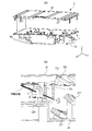
図3(a)は、本実施例におけるカバー30の構成を示す図であり、カバー30を光学箱20側から見た斜視図である。図3(a)において、カバー30には、光学箱20の外壁に設けられた突起を係合させて、スナップフィット構造を構成する複数のフック部32が設けられている。また、カバー30には、防塵窓223、224、225、226が設けられている。更に、カバー30には、光学箱20への装着時に、光学箱20の側壁により形成される外周縁と対向する部分全周に、防塵部材であるシール部31が射出成形によって形成されている。また、射出成形時に、成形部材であるポリオレフィン系の溶融したホットメルト接着剤(以下、「ホットメルト」という)を注入するゲート部31aが、図3(a)では2か所、シール部31の全長をほぼ二分する位置に設けられている。ゲート部31aは、本実施例では2か所設けられているが、実際の成形性に合わせて増減することができ、少なくとも1か所以上設けられていればよい。
図3(a)は、本実施例におけるカバー30の構成を示す図であり、カバー30を光学箱20側から見た斜視図である。図3(a)において、カバー30には、光学箱20の外壁に設けられた突起を係合させて、スナップフィット構造を構成する複数のフック部32が設けられている。また、カバー30には、防塵窓223、224、225、226が設けられている。更に、カバー30には、光学箱20への装着時に、光学箱20の側壁により形成される外周縁と対向する部分全周に、防塵部材であるシール部31が射出成形によって形成されている。また、射出成形時に、成形部材であるポリオレフィン系の溶融したホットメルト接着剤(以下、「ホットメルト」という)を注入するゲート部31aが、図3(a)では2か所、シール部31の全長をほぼ二分する位置に設けられている。ゲート部31aは、本実施例では2か所設けられているが、実際の成形性に合わせて増減することができ、少なくとも1か所以上設けられていればよい。
シール部31は、形成されたカバー30と、カバー30に当接した型との間の空間に、ポリオレフィン系のホットメルトを射出することにより、カバー30上に形成される。図3(b)は、カバー30を、図3(a)の図中に示す白抜き矢印で示すJ-J(一点鎖線)の位置で切断したJ-J断面図であり、カバー30とシール部31の関係を示す断面図である。図3(b)において、カバー30には、ゲート部31aから注入された溶融したホットメルトが流れる溝部30aが設けられており、この溝部30aにホットメルトを充填することにより、シール部31が形成される。溝部30aは、カバー30を光学箱20に取り付けることによって、シール部31が光学箱20の側壁とカバー30とによって挟まれるように形成されている。更に、溝部30aの中には、更に幅が狭くて深さの浅いアンカー溝30cが設けられ、カバー30とシール部31の接触面積を拡大させている。これにより、防塵部材であるシール部材がカバー30から意図せず剥がれたりしないように、カバー30とシール部31の間の接着性を確保している。また、シール部31の表面には、凹状の溝部が形成され、この溝部に光学箱20の側壁により形成される外周縁が挿入されることにより、光学箱20内部が防塵されると共に、光学箱20の密閉性も確保される。
図3(c)は、図3(a)において円で囲まれたカバー30の部分(ゲート部31a周辺部)を拡大した図である。シール部31を射出成形により形成する場合には、ゲート部31aから射出ノズルを介してホットメルトが注入される。そのため、図3(c)に示すように、ホットメルトの注入が終了した後、射出ノズル内に残っていた成形材料がそのまま固化して、ノズル形状のランナー部31cがゲート部31aに形成される。ゲート部31aにランナー部31cが形成されることにより、図7(b)に示したように、ランナー部31cが光学箱20内の光ビームの光路を遮ったり、光学箱20に配置された光学部品に当接して光学部品の姿勢や位置を変えてしまったりするおそれがある。
[ゲート部配置領域]
そこで、本実施例では、このランナー部31cが光走査装置21内で大きく突出していても光ビームの光路等に支障がないように、ゲート部31aを配置する領域について、図4を用いて説明する。図4は、本実施例の光走査装置21を下側(-Z軸方向)から見た図であり、光学箱20を除き、カバー30と光走査装置21内部に配置されている光学部品(レンズ、反射ミラー等)等を示した図である。
そこで、本実施例では、このランナー部31cが光走査装置21内で大きく突出していても光ビームの光路等に支障がないように、ゲート部31aを配置する領域について、図4を用いて説明する。図4は、本実施例の光走査装置21を下側(-Z軸方向)から見た図であり、光学箱20を除き、カバー30と光走査装置21内部に配置されている光学部品(レンズ、反射ミラー等)等を示した図である。
図4において、光源ユニット202(Y、M、C、Bk)から出射された光ビームは、入射光路L1を通り、ポリゴンモータ232により駆動される回転多面鏡(図4では不図示)に入射する。図4において、A側に配置された光源ユニット202は、前述した光源ユニット202Y、202Mであり、B側に配置された光源ユニット202は、前述した光源ユニット202C、202Bkである。そして、矢印方向(反時計回り方向)に回転する回転多面鏡に入射した光ビームは、走査光路L2又はL3に沿って反射ミラー212、215へと偏向される。図中、走査方向は、回転多面鏡により偏向された光ビームが走査される方向を示す。光源ユニット202Y、202Mから出射された光ビームは、図中A側(図中の右方向)へ偏向される。そして、走査光路L2は、光源ユニット202Yから出射された光ビームの反射ミラー212への走査光路を示している。光源ユニット202C、202Bkから出射された光ビームは、図中B側(図中の左方向)へ偏向される。そして、走査光路L3は、光源ユニット202Bkから出射された光ビームの反射ミラー215への走査光路を示している。なお、走査光路L2は、反射ミラー212に向かう光ビームの走査開始時、走査終了時の光路を示す。同様に、走査光路L3は、反射ミラー215に向かう光ビームの走査開始時、走査終了時の光路を示す。また、光走査装置21では、光源ユニット202から出射された光ビームを回転多面鏡(図4には不図示)により偏向させて、同期光路L4に沿って、アナモフィックレンズ230を介して同期センサ231に入射させる。同期センサ231は、入射された光ビームのタイミングに基づいて、光源ユニット202から光ビームを照射する走査開始タイミングを指示する同期信号を生成する。なお、図4のその他の符号については、図2において説明しているので、ここでの説明を省略する。
図4に示すように、光走査装置21内部には、光学部品(レンズ206~211、反射ミラー212、213、215、216等)、レンズやミラーを固定させる機械部品等が設置されている。更に、光走査装置21内部には、ポリゴンモータ232、同期センサ231等の電気部品が設置されており、光走査装置21内の空間には、光ビームが通る入射光路L1、走査光路L2、L3、同期光路L4がある。図4において、光路L1~L4はそれぞれ2本の実線により示されており、2本の実線で占められた空間である光路領域を光ビームが通る。また、走査光路L2、L3は、光走査装置21内で、走査光路の占める空間である光路領域が最も大きい光路を示している。ところで、図4において、部品も光路も存在しない破線で囲まれた領域があり、これを「ゲート部配置領域」という。ゲート部配置領域においては、ゲート部31aは、カバー30に対してゲート部31aから垂直に伸びる仮想法線と光学箱20内における光ビームの光路領域とが交差しない位置に形成されている。そのため、ゲート部配置領域にゲート部31aを設けた場合には、ゲート部31aに形成されるランナー部31cにより、光路が遮られたり、部品にランナー部31cが接触して姿勢を変えられたりすることはなくなる。本実施例では、このゲート部配置領域が4箇所あり、そのうちの2箇所にシール部31のゲート部31aを配置している。これにより、ゲート部31aにおいてランナー部31cが突出していても、光走査装置21の露光性能に何ら影響を与えることがない。
なお、光走査装置21においては、図4に示すように走査光学系の走査方向(X軸方向)と平行に反射ミラー(例えば反射ミラー212、215)や走査レンズ(例えばレンズ207、210)が配置される。更に、光学箱内の空間を有効に使うために、走査方向(X軸方向)に平行な光学箱20の外周縁(図中、短辺)の近傍には反射ミラーや走査レンズが配置されることが多い。よって、ゲート部を配置する領域は、光走査装置21の走査方向(X軸方向)に平行な辺以外の場所、すなわち走査方向に直交する方向(Y軸方向)の辺の外周縁側(長辺側)に設けることが好適である。
以上より、射出成形によってカバー30に一体的にシール部31を設けることで、別体のシール部材をカバーに貼り付ける工程をなくすことができ、シール部31のランナー部31cを切断するという追加の作業工程も不要となる。その結果、シール部材付きのカバーを作製する工程が簡便になり、部品コストも下げることができる。更に成形による効果として、シール部31の形状が一定となることから、良好な密閉性を安定して確保できる。
また、ホットメルト接着剤は射出後の凝固が比較的早いため、複数のゲート部31aを設ける場合の各ゲートの配置は、全体の流動経路をほぼ均等に分割するように配置することが望ましい。もちろん、この場合にも各ゲート部31aを光路や部品が存在しないゲート部配置領域に配置する必要がある。以上説明したように、本実施例によれば、煩雑な組立作業を必要としない簡便な構成で、シール部を射出成形することができる。
光走査装置においては、ポリゴンモータの回転によって装置内部に負圧が生じ、光走査装置外部の空気を装置内部に吸い込みやすくなることがある。そのため、光走査装置においてポリゴンモータを載置する部分を仕切り等により独立した空間とした構成の光走査装置もある。本実施例では、ポリゴンモータを設置した空間をシール部材でシールしたカバーで密閉する場合の、カバーのゲート部配置領域について説明する。
[画像形成装置の構成]
実施例2の電子写真方式の画像形成装置の一例として、レーザビームプリンタを例にあげて説明する。図5は、レーザビームプリンタ300の概略構成を示す図であり、レーザビームプリンタ300は感光ドラムを1つ有するモノクロの画像形成装置である。レーザビームプリンタ300は、光走査装置42により静電潜像が形成される感光ドラム311、感光ドラム311を一様に帯電する帯電装置317、感光ドラム311上に形成された静電潜像をトナーで現像する現像装置312を備えている。そして、感光ドラム311に現像されたトナー像をカセット316から供給された記録紙に転写部318によって転写して、記録紙に転写したトナー像を定着器314で定着した後、記録紙をトレイ315に排出する。この感光ドラム311、帯電装置317、現像装置312、転写部318が画像形成部である。また、レーザビームプリンタ300は、画像形成部による画像形成動作や、記録紙の搬送動作を制御する不図示のコントローラを備えている。
実施例2の電子写真方式の画像形成装置の一例として、レーザビームプリンタを例にあげて説明する。図5は、レーザビームプリンタ300の概略構成を示す図であり、レーザビームプリンタ300は感光ドラムを1つ有するモノクロの画像形成装置である。レーザビームプリンタ300は、光走査装置42により静電潜像が形成される感光ドラム311、感光ドラム311を一様に帯電する帯電装置317、感光ドラム311上に形成された静電潜像をトナーで現像する現像装置312を備えている。そして、感光ドラム311に現像されたトナー像をカセット316から供給された記録紙に転写部318によって転写して、記録紙に転写したトナー像を定着器314で定着した後、記録紙をトレイ315に排出する。この感光ドラム311、帯電装置317、現像装置312、転写部318が画像形成部である。また、レーザビームプリンタ300は、画像形成部による画像形成動作や、記録紙の搬送動作を制御する不図示のコントローラを備えている。
[光走査装置の概要]
図6(a)は、本実施例の光走査装置42の外観を示す斜視図である。光学箱33は、後述する仕切り壁43a、43b、43c、43dにより形成される開放面である第一の開口と、第一の開口を除いた光学箱の開放面である第二の開口を有している。そして、第一の開口は第二のカバーであるカバー34により、第二の開口は第一のカバーであるカバー35により、光学箱33は密閉される。図中、Cはカバー35の上部、Dはカバー35の下部を示す。カバー35により密閉される空間は、光走査装置42において、周囲を光学箱33と一体的に成形された仕切り壁43a、43b、43c、43dにより囲まれた空間である。仕切り壁43a、43b、43c、43dは、光学箱33の底面から立設するように設けられており、隣り合う仕切り壁は連結されている。また、仕切り壁43aには、光ビームが通過する開口部39が設けられている。そして、周囲を仕切り壁43a、43b、43c、43dにより囲まれた光学箱33の底面には、ポリゴンモータ36、ポリゴンモータ36により回転駆動される回転多面鏡37が載置されている。光源ユニット38より出射された光ビームは、カバー34により密閉された光走査装置42の内部に設けられた不図示の反射ミラーに反射した後、開口部39を介して、回転多面鏡37に入射する(図中、破線矢印で表示)。そして、回転多面鏡37に入射した光ビームは偏向され、再度、開口部39を通って、カバー34により密閉された側に入射する。
図6(a)は、本実施例の光走査装置42の外観を示す斜視図である。光学箱33は、後述する仕切り壁43a、43b、43c、43dにより形成される開放面である第一の開口と、第一の開口を除いた光学箱の開放面である第二の開口を有している。そして、第一の開口は第二のカバーであるカバー34により、第二の開口は第一のカバーであるカバー35により、光学箱33は密閉される。図中、Cはカバー35の上部、Dはカバー35の下部を示す。カバー35により密閉される空間は、光走査装置42において、周囲を光学箱33と一体的に成形された仕切り壁43a、43b、43c、43dにより囲まれた空間である。仕切り壁43a、43b、43c、43dは、光学箱33の底面から立設するように設けられており、隣り合う仕切り壁は連結されている。また、仕切り壁43aには、光ビームが通過する開口部39が設けられている。そして、周囲を仕切り壁43a、43b、43c、43dにより囲まれた光学箱33の底面には、ポリゴンモータ36、ポリゴンモータ36により回転駆動される回転多面鏡37が載置されている。光源ユニット38より出射された光ビームは、カバー34により密閉された光走査装置42の内部に設けられた不図示の反射ミラーに反射した後、開口部39を介して、回転多面鏡37に入射する(図中、破線矢印で表示)。そして、回転多面鏡37に入射した光ビームは偏向され、再度、開口部39を通って、カバー34により密閉された側に入射する。
本実施例では、図6(a)に示すように、ポリゴンモータ36が底面に載置された独立した空間の上部の開放面だけを覆うカバー35を設けている。図6(b)は、カバー35をポリゴンモータ36側(光走査装置42の底面側)から見上げた図であり、カバー35の外周縁に成形されたシール部40との位置関係がわかるように、ポリゴンモータ36の外形を重ねている。また、走査光路L5(破線にて表示)は、回転多面鏡37に入射した光ビームが反射し、偏向された光ビーム(反射光)の光路を示しており、2本の破線で占められた空間である光路領域を光ビームが通る。カバー35は、シール部40と、ゲート部40aと、ゲート部40aから注入された溶融したホットメルトが流れる流路を有している。シール部40は、カバー35と立設する仕切り壁43a、43b、43c、43dとによって挟まれ、光学箱内部を防塵するためにカバー35に成形された防塵部材である。また、ゲート部40aは、シール部40を形成するために溶融したホットメルトを注入するために用いられる。そして、注入されたホットメルトが流路を流れることによって、カバー35を光学箱33に取り付けた際に、シール部40が仕切り壁43a、43b、43c、43dとカバー35とによって挟まれるように形成される。その結果、カバー35の縁に沿って全周にシール部40が射出成形され、その成形のためのゲート部40aが設けられている。
また、本実施例においても、ゲート部40aは、実施例1と同様に、カバー35に対してゲート部40aから垂直に伸びる仮想法線と、仕切り壁43a~43dにより囲まれた光学箱33内における光ビームの光路領域とが交差しない位置に形成されている。そのため、本実施例では、ゲート部40aは、ポリゴンモータ36や走査光路L5を外れた位置に1箇所設けられているが、複数のゲート部40aを設けてもよい。その結果、本実施例においても、実施例1と同等の効果を得ることができる。すなわち、射出成形によってカバー35に一体的にシール部40を設けることで、別体のシール部材をカバーに貼り付ける工程をなくすことができ、更に、シール部40のランナー部を切断するという工程も不要となる。その結果、シール部材付きのカバーを作製する工程が簡便になり、部品コストも下げることができる。更に成形による効果として、シール部40の形状が一定となることから、良好な密閉性を確保できる。なお、カバー34についても、実施例1と同様に、カバー34により覆われる光学箱33の内部に設置された光学部材や光ビームが通る入射光路、走査光路、同期光路を外れた位置にゲート部を設けることにより、実施例1と同等の効果を得ることができる。以上説明したように、本実施例によれば、煩雑な組立作業を必要としない簡便な構成で、シール部を射出成形することができる。
本発明は上記実施の形態に制限されるものではなく、本発明の精神及び範囲から離脱することなく、様々な変更及び変形が可能である。従って、本発明の範囲を公にするために以下の請求項を添付する。
本願は、2013年10月09日提出の日本国特許出願特願2013-212157を基礎として優先権を主張するものであり、その記載内容の全てをここに援用する。
20 光学箱
30 カバー
31 シール部
31a ゲート部
202 光源ユニット
203 回転多面鏡
30 カバー
31 シール部
31a ゲート部
202 光源ユニット
203 回転多面鏡
Claims (14)
- 光ビームを出射する光源と、前記光源から出射された光ビームが感光体上を走査するように前記光ビームを偏向する回転多面鏡と、前記回転多面鏡によって偏向された前記光ビームを前記感光体に導く光学部材と、前記光源、前記回転多面鏡、及び前記光学部材を収容する光学箱と、前記光学箱の開口を覆うカバーと、を備える光走査装置であって、
前記カバーは、
前記カバーと前記光学箱の側壁とによって挟まれ、光学箱内部を防塵するために前記カバーに成形された防塵部材と、
溶融した前記防塵部材を注入するためのゲート部と、
前記ゲート部から注入された溶融した前記防塵部材が流れる流路であって、前記カバーを前記光学箱に取り付けることによって前記防塵部材が前記側壁と前記カバーとによって挟まれるように前記カバーに形成された流路と、を有し、
前記ゲート部は、前記回転多面鏡の回転軸方向から見て前記光ビームの光路領域の外に設けられることを特徴とする光走査装置。 - 光ビームを出射する光源と、前記光源から出射された光ビームが感光体上を走査するように前記光ビームを偏向する回転多面鏡と、前記回転多面鏡によって偏向された前記光ビームを前記感光体に導く光学部材と、前記光源、前記回転多面鏡、及び前記光学部材を収容する光学箱と、前記光学箱の開口を覆うカバーと、を備える光走査装置であって、
前記カバーは、
前記カバーと前記光学箱の側壁とによって挟まれ、光学箱内部を防塵するために前記カバーに成形された防塵部材と、
溶融した前記防塵部材を注入するためのゲート部と、
前記ゲート部から注入された溶融した前記防塵部材が流れる流路であって、前記カバーを前記光学箱に取り付けることによって前記防塵部材が前記側壁と前記カバーとによって挟まれるように前記カバーに形成された流路と、を有し、
前記ゲート部は、前記カバーに対して前記ゲート部から垂直に伸びる仮想法線と前記光学箱内における光ビームの光路領域とが交差しない位置に形成されていることを特徴とする光走査装置。 - 前記光ビームの前記光路領域は、前記光源から出射された光ビームが前記回転多面鏡に入射する光路である入射光路、前記回転多面鏡によって偏向された前記光ビームが前記光学部材に入射する光路である走査光路、及び前記回転多面鏡によって偏向された前記光ビームが同期信号を生成するためのセンサに入射する光路である同期光路が占める領域であることを特徴とする請求項1又は2に記載の光走査装置。
- 前記ゲート部は、前記カバーに1つ以上設けられていることを特徴とする請求項1ないし3のいずれか1項に記載の光走査装置。
- 前記カバーの前記ゲート部に対向する前記光学箱の底部には、前記光学部材が設置されていないことを特徴とする請求項1ないし4のいずれか1項に記載の光走査装置。
- 前記光学部材は、前記回転多面鏡によって偏向された前記光ビームの走査方向に平行に配置されていることを特徴とする請求項1ないし5のいずれか1項に記載の光走査装置。
- 前記ゲート部は、前記光ビームの前記走査方向に直交する前記光学箱の外周縁に対向する前記カバーの外周縁側に設けられることを特徴とする請求項6に記載の光走査装置。
- 光ビームを出射する光源と、前記光源から出射された光ビームが感光体上を走査するように前記光ビームを偏向する回転多面鏡と、前記回転多面鏡によって偏向された前記光ビームを前記感光体に導く光学部材と、前記光源、前記回転多面鏡、及び前記光学部材を収容する光学箱と、前記光学箱の開口を覆うカバーと、を備える光走査装置であって、
前記光学箱は、前記光学箱の底部に設置された前記回転多面鏡を囲むように前記底部から立設する壁を有し、
前記カバーは、
前記壁で囲まれた開口であって、前記回転多面鏡を前記底部に設置する際に前記回転多面鏡を通過させる第一の開口を覆う第一のカバーと、前記第一の開口を除く前記光学箱の開口である第二の開口を覆う第二のカバーと、から構成され、
前記第一のカバーは、
前記第一のカバーと前記立設する壁とによって挟まれ、光学箱内部を防塵するために前記第一のカバーに成形された防塵部材と、
溶融した前記防塵部材を注入するためのゲート部と、
前記ゲート部から注入された溶融した前記防塵部材が流れる流路であって、前記第一のカバーを前記光学箱に取り付けることによって前記防塵部材が前記立設する壁と前記第一のカバーとによって挟まれるように前記第一のカバーに形成された流路と、を有し、
前記ゲート部は、前記回転多面鏡の回転軸方向から見て前記光ビームの光路領域の外に設けられることを特徴とする光走査装置。 - 光ビームを出射する光源と、前記光源から出射された光ビームが感光体上を走査するように前記光ビームを偏向する回転多面鏡と、前記回転多面鏡によって偏向された前記光ビームを前記感光体に導く光学部材と、前記光源、前記回転多面鏡、及び前記光学部材を収容する光学箱と、前記光学箱の開口を覆うカバーと、を備える光走査装置であって、
前記光学箱は、前記光学箱の底部に設置された前記回転多面鏡を囲むように前記底部から立設する壁を有し、
前記カバーは、前記壁で囲まれた開口であって、前記回転多面鏡を前記底部に設置する際に前記回転多面鏡を通過させる第一の開口を覆う第一のカバーと、前記第一の開口を除く前記光学箱の開口である第二の開口を覆う第二のカバーと、から構成され、
前記第一のカバーは、
前記第一のカバーと前記立設する壁とによって挟まれ、光学箱内部を防塵するために前記第一のカバーに成形された防塵部材と、
溶融した前記防塵部材を注入するためのゲート部と、
前記ゲート部から注入された溶融した前記防塵部材が流れる流路であって、前記第一のカバーを前記光学箱に取り付けることによって前記防塵部材が前記立設する壁と前記第一のカバーとによって挟まれるように前記第一のカバーに形成された流路と、を有し、
前記ゲート部は、前記第一のカバーに対して前記ゲート部から垂直に伸びる仮想法線と前記光学箱内における光ビームの光路領域とが交差しない位置に形成されていることを特徴とする光走査装置。 - 前記壁は、前記光学箱と一体的に成形されることを特徴とする請求項8又は9に記載の光走査装置。
- 前記壁は、前記光ビームが通過する開口部を有し、
前記光ビームの前記光路領域は、前記光源から出射された光ビームが前記開口部を通って前記回転多面鏡に入射する光路である入射光路、及び前記回転多面鏡によって偏向された前記光ビームが前記開口部に入射する光路である走査光路が占める領域であることを特徴とする請求項8ないし10のいずれか1項に記載の光走査装置。 - 前記ゲート部は、前記第一のカバーに1つ以上設けられていることを特徴とする請求項8ないし11のいずれか1項に記載の光走査装置。
- 前記第一のカバーの前記ゲート部に対向する前記光学箱の底部には、前記回転多面鏡が設置されていないことを特徴とする請求項8ないし12のいずれか1項に記載の光走査装置。
- 請求項1ないし13のいずれか1項に記載の光走査装置と、
前記光走査装置から走査された光ビームにより静電潜像が形成される前記感光体と、
前記感光体上に形成された静電潜像を現像する現像手段と、
を備えることを特徴とする画像形成装置。
Priority Applications (3)
| Application Number | Priority Date | Filing Date | Title |
|---|---|---|---|
| CN201910177913.3A CN109901287B (zh) | 2013-10-09 | 2014-09-26 | 光学扫描设备和图像形成装置 |
| US15/027,417 US10409190B2 (en) | 2013-10-09 | 2014-09-26 | Optical scanning device and image forming apparatus |
| CN201480055496.0A CN105612455A (zh) | 2013-10-09 | 2014-09-26 | 光学扫描设备和图像形成装置 |
Applications Claiming Priority (2)
| Application Number | Priority Date | Filing Date | Title |
|---|---|---|---|
| JP2013212157A JP6242142B2 (ja) | 2013-10-09 | 2013-10-09 | 光走査装置及び画像形成装置 |
| JP2013-212157 | 2013-10-09 |
Publications (1)
| Publication Number | Publication Date |
|---|---|
| WO2015053095A1 true WO2015053095A1 (ja) | 2015-04-16 |
Family
ID=52812914
Family Applications (1)
| Application Number | Title | Priority Date | Filing Date |
|---|---|---|---|
| PCT/JP2014/075589 Ceased WO2015053095A1 (ja) | 2013-10-09 | 2014-09-26 | 光走査装置及び画像形成装置 |
Country Status (4)
| Country | Link |
|---|---|
| US (1) | US10409190B2 (ja) |
| JP (1) | JP6242142B2 (ja) |
| CN (2) | CN105612455A (ja) |
| WO (1) | WO2015053095A1 (ja) |
Families Citing this family (9)
| Publication number | Priority date | Publication date | Assignee | Title |
|---|---|---|---|---|
| JP6576158B2 (ja) * | 2015-08-19 | 2019-09-18 | キヤノン株式会社 | 光走査装置及び画像形成装置 |
| JP6608225B2 (ja) * | 2015-09-08 | 2019-11-20 | キヤノン株式会社 | 光走査装置 |
| JP6840562B2 (ja) * | 2017-02-15 | 2021-03-10 | キヤノン株式会社 | 光走査装置及び画像形成装置 |
| JP7423229B2 (ja) * | 2019-09-13 | 2024-01-29 | キヤノン株式会社 | 光学走査装置及びこれを搭載する画像形成装置 |
| JP7598556B2 (ja) | 2021-03-12 | 2024-12-12 | 株式会社リコー | 筐体構造、光走査装置及び画像形成装置 |
| JP7602959B2 (ja) | 2021-04-27 | 2024-12-19 | シャープ株式会社 | ハウジングカバー、光学箱および画像形成装置 |
| US12088765B2 (en) | 2022-03-22 | 2024-09-10 | Ricoh Company, Ltd. | Casing structure, optical scanner, and image forming apparatus |
| CN116859690B (zh) * | 2023-07-10 | 2024-08-02 | 虎丘影像(苏州)股份有限公司 | 一种曝光装置 |
| JP2025115512A (ja) * | 2024-01-26 | 2025-08-07 | キヤノン株式会社 | 光学走査装置及び画像形成装置 |
Citations (4)
| Publication number | Priority date | Publication date | Assignee | Title |
|---|---|---|---|---|
| JP2002341275A (ja) * | 2001-05-15 | 2002-11-27 | Canon Inc | 偏向走査装置 |
| JP2009063833A (ja) * | 2007-09-06 | 2009-03-26 | Ricoh Co Ltd | 画像形成装置 |
| JP2009237552A (ja) * | 2008-03-06 | 2009-10-15 | Canon Inc | 走査光学装置 |
| JP2012008250A (ja) * | 2010-06-23 | 2012-01-12 | Ricoh Co Ltd | 画像形成装置 |
Family Cites Families (11)
| Publication number | Priority date | Publication date | Assignee | Title |
|---|---|---|---|---|
| US6490072B2 (en) * | 2001-01-12 | 2002-12-03 | Lexmark International, Inc. | Mirror angle adjustment and mounting system for a laser scanner device |
| US6969846B2 (en) | 2002-02-28 | 2005-11-29 | Canon Kabushiki Kaisha | Light source unit and scanning optical apparatus using the same |
| JP2004021133A (ja) | 2002-06-20 | 2004-01-22 | Canon Inc | 走査光学装置 |
| JP4403696B2 (ja) * | 2002-12-12 | 2010-01-27 | 富士ゼロックス株式会社 | 光走査装置 |
| JP2004262118A (ja) | 2003-03-03 | 2004-09-24 | Ricoh Co Ltd | 書込み装置および画像形成装置 |
| US7443415B2 (en) * | 2005-08-04 | 2008-10-28 | Kabushiki Kaisha Toshiba | Optical beam scanning device and image forming apparatus having window for polygon mirror cover |
| US7755655B2 (en) * | 2006-05-12 | 2010-07-13 | Kyocera Mita Corporation | Exposure device and image forming apparatus |
| JP5247371B2 (ja) * | 2008-11-19 | 2013-07-24 | キヤノン株式会社 | 走査光学装置及びこれを備える画像形成装置 |
| JP5153854B2 (ja) * | 2010-11-15 | 2013-02-27 | シャープ株式会社 | 画像形成装置 |
| JP2013113957A (ja) * | 2011-11-28 | 2013-06-10 | Canon Inc | 光走査装置および画像形成装置 |
| JP6288995B2 (ja) * | 2013-09-06 | 2018-03-07 | キヤノン株式会社 | 光走査装置及び画像形成装置 |
-
2013
- 2013-10-09 JP JP2013212157A patent/JP6242142B2/ja not_active Expired - Fee Related
-
2014
- 2014-09-26 CN CN201480055496.0A patent/CN105612455A/zh active Pending
- 2014-09-26 WO PCT/JP2014/075589 patent/WO2015053095A1/ja not_active Ceased
- 2014-09-26 US US15/027,417 patent/US10409190B2/en active Active
- 2014-09-26 CN CN201910177913.3A patent/CN109901287B/zh not_active Expired - Fee Related
Patent Citations (4)
| Publication number | Priority date | Publication date | Assignee | Title |
|---|---|---|---|---|
| JP2002341275A (ja) * | 2001-05-15 | 2002-11-27 | Canon Inc | 偏向走査装置 |
| JP2009063833A (ja) * | 2007-09-06 | 2009-03-26 | Ricoh Co Ltd | 画像形成装置 |
| JP2009237552A (ja) * | 2008-03-06 | 2009-10-15 | Canon Inc | 走査光学装置 |
| JP2012008250A (ja) * | 2010-06-23 | 2012-01-12 | Ricoh Co Ltd | 画像形成装置 |
Also Published As
| Publication number | Publication date |
|---|---|
| CN109901287A (zh) | 2019-06-18 |
| JP2015075654A (ja) | 2015-04-20 |
| US10409190B2 (en) | 2019-09-10 |
| CN109901287B (zh) | 2022-06-28 |
| JP6242142B2 (ja) | 2017-12-06 |
| CN105612455A (zh) | 2016-05-25 |
| US20160246207A1 (en) | 2016-08-25 |
Similar Documents
| Publication | Publication Date | Title |
|---|---|---|
| JP6242142B2 (ja) | 光走査装置及び画像形成装置 | |
| JP5264555B2 (ja) | 走査光学装置 | |
| US9063501B2 (en) | Developer accommodating unit with light guide member for detecting remaining toner amount | |
| JP6576158B2 (ja) | 光走査装置及び画像形成装置 | |
| JP6288995B2 (ja) | 光走査装置及び画像形成装置 | |
| JP2018132642A (ja) | 光走査装置の筐体及び光走査装置 | |
| JP4922790B2 (ja) | 光走査装置および画像形成装置 | |
| JP4925623B2 (ja) | 光走査装置及び画像形成装置 | |
| JP6608225B2 (ja) | 光走査装置 | |
| JP7051472B2 (ja) | 光走査装置及び画像形成装置 | |
| JP6226651B2 (ja) | 光走査装置及び画像形成装置 | |
| JP6080625B2 (ja) | 画像形成装置 | |
| JP6188501B2 (ja) | 光走査装置及び画像形成装置 | |
| US12443124B2 (en) | Optical scanning device and image forming apparatus mounted with it | |
| JP7051473B2 (ja) | 光走査装置及び画像形成装置 | |
| JP6739917B2 (ja) | 画像形成装置および光学走査装置 | |
| JP2023140267A (ja) | 筐体部構造、光走査装置及び画像形成装置 | |
| JP2007233279A (ja) | 画像形成装置 | |
| JP2023028648A (ja) | 光走査装置及び画像形成装置 | |
| JP2017049317A (ja) | 光走査装置及び画像形成装置 |
Legal Events
| Date | Code | Title | Description |
|---|---|---|---|
| 121 | Ep: the epo has been informed by wipo that ep was designated in this application |
Ref document number: 14852098 Country of ref document: EP Kind code of ref document: A1 |
|
| WWE | Wipo information: entry into national phase |
Ref document number: 15027417 Country of ref document: US |
|
| NENP | Non-entry into the national phase |
Ref country code: DE |
|
| 122 | Ep: pct application non-entry in european phase |
Ref document number: 14852098 Country of ref document: EP Kind code of ref document: A1 |