WO2015045694A1 - 液晶表示装置 - Google Patents
液晶表示装置 Download PDFInfo
- Publication number
- WO2015045694A1 WO2015045694A1 PCT/JP2014/071957 JP2014071957W WO2015045694A1 WO 2015045694 A1 WO2015045694 A1 WO 2015045694A1 JP 2014071957 W JP2014071957 W JP 2014071957W WO 2015045694 A1 WO2015045694 A1 WO 2015045694A1
- Authority
- WO
- WIPO (PCT)
- Prior art keywords
- liquid crystal
- crystal display
- display device
- crystal layer
- display panel
- Prior art date
- Legal status (The legal status is an assumption and is not a legal conclusion. Google has not performed a legal analysis and makes no representation as to the accuracy of the status listed.)
- Ceased
Links
Images







Classifications
-
- G—PHYSICS
- G02—OPTICS
- G02F—OPTICAL DEVICES OR ARRANGEMENTS FOR THE CONTROL OF LIGHT BY MODIFICATION OF THE OPTICAL PROPERTIES OF THE MEDIA OF THE ELEMENTS INVOLVED THEREIN; NON-LINEAR OPTICS; FREQUENCY-CHANGING OF LIGHT; OPTICAL LOGIC ELEMENTS; OPTICAL ANALOGUE/DIGITAL CONVERTERS
- G02F1/00—Devices or arrangements for the control of the intensity, colour, phase, polarisation or direction of light arriving from an independent light source, e.g. switching, gating or modulating; Non-linear optics
- G02F1/01—Devices or arrangements for the control of the intensity, colour, phase, polarisation or direction of light arriving from an independent light source, e.g. switching, gating or modulating; Non-linear optics for the control of the intensity, phase, polarisation or colour
- G02F1/13—Devices or arrangements for the control of the intensity, colour, phase, polarisation or direction of light arriving from an independent light source, e.g. switching, gating or modulating; Non-linear optics for the control of the intensity, phase, polarisation or colour based on liquid crystals, e.g. single liquid crystal display cells
- G02F1/133—Constructional arrangements; Operation of liquid crystal cells; Circuit arrangements
- G02F1/1333—Constructional arrangements; Manufacturing methods
- G02F1/1339—Gaskets; Spacers; Sealing of cells
-
- G—PHYSICS
- G02—OPTICS
- G02F—OPTICAL DEVICES OR ARRANGEMENTS FOR THE CONTROL OF LIGHT BY MODIFICATION OF THE OPTICAL PROPERTIES OF THE MEDIA OF THE ELEMENTS INVOLVED THEREIN; NON-LINEAR OPTICS; FREQUENCY-CHANGING OF LIGHT; OPTICAL LOGIC ELEMENTS; OPTICAL ANALOGUE/DIGITAL CONVERTERS
- G02F1/00—Devices or arrangements for the control of the intensity, colour, phase, polarisation or direction of light arriving from an independent light source, e.g. switching, gating or modulating; Non-linear optics
- G02F1/01—Devices or arrangements for the control of the intensity, colour, phase, polarisation or direction of light arriving from an independent light source, e.g. switching, gating or modulating; Non-linear optics for the control of the intensity, phase, polarisation or colour
- G02F1/13—Devices or arrangements for the control of the intensity, colour, phase, polarisation or direction of light arriving from an independent light source, e.g. switching, gating or modulating; Non-linear optics for the control of the intensity, phase, polarisation or colour based on liquid crystals, e.g. single liquid crystal display cells
- G02F1/133—Constructional arrangements; Operation of liquid crystal cells; Circuit arrangements
- G02F1/1333—Constructional arrangements; Manufacturing methods
- G02F1/133377—Cells with plural compartments or having plurality of liquid crystal microcells partitioned by walls, e.g. one microcell per pixel
-
- G—PHYSICS
- G02—OPTICS
- G02F—OPTICAL DEVICES OR ARRANGEMENTS FOR THE CONTROL OF LIGHT BY MODIFICATION OF THE OPTICAL PROPERTIES OF THE MEDIA OF THE ELEMENTS INVOLVED THEREIN; NON-LINEAR OPTICS; FREQUENCY-CHANGING OF LIGHT; OPTICAL LOGIC ELEMENTS; OPTICAL ANALOGUE/DIGITAL CONVERTERS
- G02F1/00—Devices or arrangements for the control of the intensity, colour, phase, polarisation or direction of light arriving from an independent light source, e.g. switching, gating or modulating; Non-linear optics
- G02F1/01—Devices or arrangements for the control of the intensity, colour, phase, polarisation or direction of light arriving from an independent light source, e.g. switching, gating or modulating; Non-linear optics for the control of the intensity, phase, polarisation or colour
- G02F1/13—Devices or arrangements for the control of the intensity, colour, phase, polarisation or direction of light arriving from an independent light source, e.g. switching, gating or modulating; Non-linear optics for the control of the intensity, phase, polarisation or colour based on liquid crystals, e.g. single liquid crystal display cells
- G02F1/133—Constructional arrangements; Operation of liquid crystal cells; Circuit arrangements
- G02F1/1333—Constructional arrangements; Manufacturing methods
- G02F1/1335—Structural association of cells with optical devices, e.g. polarisers or reflectors
- G02F1/133528—Polarisers
-
- G—PHYSICS
- G02—OPTICS
- G02F—OPTICAL DEVICES OR ARRANGEMENTS FOR THE CONTROL OF LIGHT BY MODIFICATION OF THE OPTICAL PROPERTIES OF THE MEDIA OF THE ELEMENTS INVOLVED THEREIN; NON-LINEAR OPTICS; FREQUENCY-CHANGING OF LIGHT; OPTICAL LOGIC ELEMENTS; OPTICAL ANALOGUE/DIGITAL CONVERTERS
- G02F1/00—Devices or arrangements for the control of the intensity, colour, phase, polarisation or direction of light arriving from an independent light source, e.g. switching, gating or modulating; Non-linear optics
- G02F1/01—Devices or arrangements for the control of the intensity, colour, phase, polarisation or direction of light arriving from an independent light source, e.g. switching, gating or modulating; Non-linear optics for the control of the intensity, phase, polarisation or colour
- G02F1/13—Devices or arrangements for the control of the intensity, colour, phase, polarisation or direction of light arriving from an independent light source, e.g. switching, gating or modulating; Non-linear optics for the control of the intensity, phase, polarisation or colour based on liquid crystals, e.g. single liquid crystal display cells
- G02F1/133—Constructional arrangements; Operation of liquid crystal cells; Circuit arrangements
- G02F1/1333—Constructional arrangements; Manufacturing methods
- G02F1/1337—Surface-induced orientation of the liquid crystal molecules, e.g. by alignment layers
-
- G—PHYSICS
- G02—OPTICS
- G02F—OPTICAL DEVICES OR ARRANGEMENTS FOR THE CONTROL OF LIGHT BY MODIFICATION OF THE OPTICAL PROPERTIES OF THE MEDIA OF THE ELEMENTS INVOLVED THEREIN; NON-LINEAR OPTICS; FREQUENCY-CHANGING OF LIGHT; OPTICAL LOGIC ELEMENTS; OPTICAL ANALOGUE/DIGITAL CONVERTERS
- G02F1/00—Devices or arrangements for the control of the intensity, colour, phase, polarisation or direction of light arriving from an independent light source, e.g. switching, gating or modulating; Non-linear optics
- G02F1/01—Devices or arrangements for the control of the intensity, colour, phase, polarisation or direction of light arriving from an independent light source, e.g. switching, gating or modulating; Non-linear optics for the control of the intensity, phase, polarisation or colour
- G02F1/13—Devices or arrangements for the control of the intensity, colour, phase, polarisation or direction of light arriving from an independent light source, e.g. switching, gating or modulating; Non-linear optics for the control of the intensity, phase, polarisation or colour based on liquid crystals, e.g. single liquid crystal display cells
- G02F1/133—Constructional arrangements; Operation of liquid crystal cells; Circuit arrangements
- G02F1/1333—Constructional arrangements; Manufacturing methods
- G02F1/1339—Gaskets; Spacers; Sealing of cells
- G02F1/13394—Gaskets; Spacers; Sealing of cells spacers regularly patterned on the cell subtrate, e.g. walls, pillars
-
- G—PHYSICS
- G02—OPTICS
- G02F—OPTICAL DEVICES OR ARRANGEMENTS FOR THE CONTROL OF LIGHT BY MODIFICATION OF THE OPTICAL PROPERTIES OF THE MEDIA OF THE ELEMENTS INVOLVED THEREIN; NON-LINEAR OPTICS; FREQUENCY-CHANGING OF LIGHT; OPTICAL LOGIC ELEMENTS; OPTICAL ANALOGUE/DIGITAL CONVERTERS
- G02F1/00—Devices or arrangements for the control of the intensity, colour, phase, polarisation or direction of light arriving from an independent light source, e.g. switching, gating or modulating; Non-linear optics
- G02F1/01—Devices or arrangements for the control of the intensity, colour, phase, polarisation or direction of light arriving from an independent light source, e.g. switching, gating or modulating; Non-linear optics for the control of the intensity, phase, polarisation or colour
- G02F1/13—Devices or arrangements for the control of the intensity, colour, phase, polarisation or direction of light arriving from an independent light source, e.g. switching, gating or modulating; Non-linear optics for the control of the intensity, phase, polarisation or colour based on liquid crystals, e.g. single liquid crystal display cells
- G02F1/133—Constructional arrangements; Operation of liquid crystal cells; Circuit arrangements
- G02F1/1333—Constructional arrangements; Manufacturing methods
- G02F1/133388—Constructional arrangements; Manufacturing methods with constructional differences between the display region and the peripheral region
Definitions
- the present invention relates to a liquid crystal display device. More specifically, the present invention relates to a liquid crystal display device suitable for a display device for a gaming machine such as a slot machine.
- Liquid crystal display devices are used in various fields as display devices for OA equipment such as personal computers and information terminal equipment, taking advantage of features such as light weight, thinness, and low power consumption. In recent years, liquid crystal display devices are also used in gaming machines such as slot machines. A liquid crystal display device for gaming machines is provided, for example, on the front surface of the casing of the gaming machine.
- a liquid crystal display panel included in a liquid crystal display device for gaming machines has a video display unit capable of displaying video, and basically has the same structure as that of a normal use, but a transmission unit at the center of the video display unit have.
- a player can visually recognize a rotating reel housed inside the casing through the transmissive portion from the outside.
- an object that can be viewed by an observer through the transmission part of the liquid crystal display panel is also referred to as a display object.
- the display object is disposed behind the liquid crystal display device and the liquid crystal display panel.
- liquid crystal display devices or gaming machines for gaming machines for example, the following are disclosed.
- a liquid crystal display device comprising a transmissive liquid crystal display panel disposed on the front side of a rotating reel, and a backlight disposed between the liquid crystal display panel and the rotating reel and illuminating the liquid crystal display panel from the back side.
- the liquid crystal display panel is a liquid crystal display device having an image display unit configured to display an image by enclosing a liquid crystal material between a pair of substrates, and a transmission unit not enclosing the liquid crystal material facing the rotating reel. (For example, refer to Patent Document 1).
- a liquid crystal display device comprising a transmissive liquid crystal display panel disposed on the front side of a display medium for variable display, and a pair of polarizing plates respectively disposed on the outer surface of the liquid crystal display panel, the liquid crystal display panel comprising: A video display unit configured to display video, a substantially rectangular transmissive display unit corresponding to an area in which the display medium is disposed, and a light shielding unit disposed between the video display unit and the transmissive display unit.
- Each of the pair of polarizing plates has a substantially rectangular opening corresponding to a region where the display medium is disposed, and a liquid crystal display in which an edge defining the opening is located on the light shielding portion of the liquid crystal display panel
- An apparatus is disclosed (for example, refer to Patent Document 2).
- a main reel device having a liquid crystal display panel in the effect panel portion, a sub reel device having a sub reel provided on the back side of the display window formed in the liquid crystal display panel, and a main reel above the effect panel portion has been disclosed (see, for example, Patent Documents 4 to 6).
- a liquid crystal display device having a fixed display portion in which a colored layer of a predetermined pattern is formed has been developed.
- a liquid crystal cell for example, a liquid crystal cell, a polarizing member provided on at least one of the front side and the rear side of the liquid crystal cell, and a front side polarization
- a fixed display portion comprising a first light-transmitting substrate provided in front of the member, a first light-transmitting colored layer formed on the first light-transmitting substrate, and a fixed display of at least one of the polarizing members
- a liquid crystal display device having a polarizing member removing unit excluding a portion corresponding to the unit is disclosed (for example, see Patent Document 7).
- a liquid crystal display device having a structure in which another display object such as a meter or a rotating reel disposed behind can be visually recognized through the transmission part of the liquid crystal display panel, the transmittance of the transmission part is improved and the rear display object is visually recognized. If an opening is formed in the polarizing plate corresponding to the transmissive portion in order to improve the property, display defects such as spots and unevenness occur in the video display portion around the transmissive portion.
- the reason for this is as follows. That is, since the polarizing plate has a function of shielding ultraviolet light, the liquid crystal of the image display unit is not irradiated with ultraviolet light. However, if an opening is formed in the polarizing plate corresponding to the transmissive part, the ultraviolet light contained in the external light and / or the ultraviolet light contained in the light of the display object illumination behind is irradiated to the liquid crystal in the transmissive part. , The liquid crystal in the transmission part deteriorates. Then, the deteriorated liquid crystal diffuses to the video display unit, and as a result, display defects such as spots and unevenness occur in the video display unit.
- Patent Document 2 describes that even if a display defect occurs in the vicinity of the video display unit, the light can be blocked by a light shielding unit provided between the video display unit and the transmission unit.
- the liquid crystal in the transmission part deteriorates due to ultraviolet light
- the deteriorated liquid crystal diffuses beyond the light-shielding part to the video display part over a long period of use, and display defects such as spots and unevenness may occur.
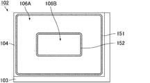
- FIG. 13 is a schematic plan view of a liquid crystal display panel included in the liquid crystal display device described in Patent Document 1.
- the liquid crystal display device described in Patent Document 1 includes a liquid crystal display panel 102.
- the liquid crystal display panel 102 includes a pair of an array substrate 103 and a counter substrate 104, and an array substrate 103 and a counter substrate 104.
- the image display unit 106A is formed in a region surrounded by the loop-shaped first seal 151 and the loop-shaped second seal 152 disposed inside the first seal 151, and the transmission unit 106B. Is formed in a region surrounded by the second seal 152.
- FIG. 14 is a schematic plan view of a liquid crystal display panel included in the liquid crystal display device described in Patent Document 1.
- 15 and 16 are schematic cross-sectional views of a liquid crystal display panel included in the liquid crystal display device described in Patent Document 1.
- FIG. 14 is a schematic plan view of a liquid crystal display panel included in the liquid crystal display device described in Patent Document 1.
- 15 and 16 are schematic cross-sectional views of a liquid crystal display panel included in the liquid crystal display device described in Patent Document 1.
- the seal break 153 occurs, the liquid crystal material cannot be sealed in a certain region by the second seal 152, and the liquid crystal material leaks from the image display unit 106A to the transmission unit 106B. Therefore, cell thickness unevenness occurs in the video display unit 106A. Further, impurities enter the liquid crystal material from the portion where the seal break 153 occurs, and the liquid crystal material deteriorates. Accordingly, the seal break 153 causes display defects such as spots and unevenness in the image display unit 106A. Further, when the liquid crystal material leaks to the transmission part 106B, the liquid crystal material is not aligned in the transmission part 106B, and thus scattering occurs in the light transmitted through the liquid crystal material. Therefore, the seal break 153 causes unevenness in the transmittance of the transmission part 106B.
- the seal blowout 154 occurs, a part of the second seal 152 spreads beyond the original formation region. For this reason, when the second seal 152 blows out to the video display unit 106A, the second seal 152 that has entered the video display unit 106A may cause a lighting failure in that portion. Further, the second seal 152 before curing is mixed in the liquid crystal material of the image display unit 106A, and the liquid crystal material is deteriorated. Therefore, the sticker balloon 154 causes display defects such as spots and unevenness in the video display unit 106A. On the other hand, when the second seal 152 spreads to the transmission part 106B, the unevenness of the transmittance is caused in the spread part of the second seal 152.
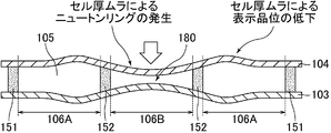
- the external pressure applied to the transmission part 106B (the white area in FIG.
- the cell internal pressure of the transmission part 106B becomes lower than the arrow), that is, the cell internal pressure of the transmission part 106B becomes negative.
- the cell thickness of the transmission part 106B becomes thin.
- the cell thickness unevenness of the transmissive portion 106B may affect the cell thickness of the video display portion 106A. In this case, the display quality of the video display portion 106A is reduced.
- the transmissive part 106B In order to improve the transmittance of the transmissive part 106B, in the transmissive part 106B, components of the counter substrate 104 such as a black matrix (BM) and a color filter and / or an array substrate such as a pixel electrode and a wiring If the constituent member 103 is deleted, the total thickness of the constituent members of the counter substrate 104 and / or the array substrate 103 above and below the spacer is different between the transmission portion 106B and the image display portion 106A. Therefore, the cell thickness cannot be kept uniform between the video display unit 106A and the transmission unit 106B. Further, as described above, since the cell internal pressure of the transmission part 106B is a negative pressure, the influence due to the reduction of the constituent members becomes significant. For this reason, the constituent members of the counter substrate 104 and / or the array substrate 103 cannot be deleted above and below the spacer of the transmissive portion 106B, and the transmittance of the transmissive portion 106B cannot be improved. Can not improve
- the present invention has been made in view of the above-described situation, and suppresses display defects in the video display unit, improves display quality in the video display unit and the transmission unit, improves visibility in the transmission unit, and long-term reliability.
- An object of the present invention is to provide a liquid crystal display device capable of improving the above.
- One embodiment of the present invention may be a liquid crystal display device including a liquid crystal display panel.
- the liquid crystal display panel has a transmissive portion that can be seen behind the liquid crystal display panel;
- a video display unit including a plurality of pixels and capable of displaying video;
- a first liquid crystal layer provided corresponding to the video display unit;
- a second liquid crystal layer provided corresponding to the transmission part;
- the first liquid crystal layer and the second liquid crystal layer may be separated by the seal.
- this liquid crystal display device is also referred to as a liquid crystal display device according to the present invention.
- the second liquid crystal layer may include an unaligned liquid crystal.
- the second liquid crystal layer may include an aligned liquid crystal.
- the liquid crystal display panel may include a pair of substrates that sandwich the first liquid crystal layer and the second liquid crystal layer, Each of the pair of substrates may include an alignment film provided on the video display unit and the transmission unit, The alignment film may be subjected to an alignment process in the same manner in the image display unit and the transmission unit, or may not be subjected to an alignment process in the image display unit and the transmission unit.
- the liquid crystal display panel includes a plurality of first spacers provided in the video display unit, It may include a plurality of second spacers provided in the transmission part, The arrangement density and / or contact area of the plurality of second spacers may be smaller than the arrangement density and / or contact area of the plurality of first spacers, respectively.
- the liquid crystal display panel includes a pair of substrates that sandwich the first liquid crystal layer and the second liquid crystal layer; A first spacer provided in the video display unit; A second spacer provided in the transmission part, At least one of the pair of substrates may include an insulating substrate and a constituent member provided between the insulating substrate and the first spacer, and the constituent member is provided between the insulating substrate and the second spacer. It is not necessary to include a constituent member formed from the same material.
- the liquid crystal display panel may include a pair of substrates that sandwich the first liquid crystal layer and the second liquid crystal layer, The structure of at least one of the pair of substrates may be different between the image display unit and the transmission unit.
- one of the pair of substrates may include at least one of a color filter layer, a black matrix, and a counter electrode,
- the at least one of the color filter layer, the black matrix, and the counter electrode may be provided in the video display unit without being provided in the transmission unit.
- the liquid crystal display device may include a pair of polarizing plates provided on the front and back surfaces of the liquid crystal display panel, At least one of the pair of polarizing plates may be provided so as not to overlap the transmission part and to overlap the video display part.
- both of the pair of polarizing plates may be provided so as not to overlap the transmission part and to overlap the video display part.
- a liquid crystal display device capable of suppressing display defects in the video display unit, improving display quality in the video display unit and the transmission unit, improving visibility in the transmission unit, and improving long-term reliability. Can be realized.
- FIG. 1 is a perspective exploded schematic view of a liquid crystal display device of Embodiment 1.
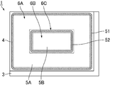
- FIG. 2 is a schematic plan view of a liquid crystal display panel included in the liquid crystal display device of Embodiment 1.
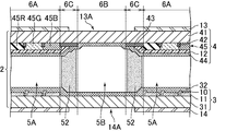
- FIG. 3 is a schematic cross-sectional view of a liquid crystal display panel included in the liquid crystal display device of Embodiment 1.
- FIG. 3 is a perspective exploded schematic view of a backlight included in the liquid crystal display device of Embodiment 1.
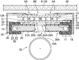
- FIG. 1 is a schematic cross-sectional view of a gaming machine including a liquid crystal display device of Embodiment 1.
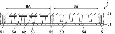
- FIG. 6 is a schematic cross-sectional view of a liquid crystal display panel included in the liquid crystal display device of Embodiment 2.
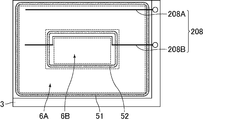
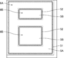
- FIG. 6 is a schematic plan view of a liquid crystal display panel included in a liquid crystal display device of Embodiment 2.
- FIG. 6 is a schematic cross-sectional view of a liquid crystal display panel included in a liquid crystal display device of Embodiment 3.
- FIG. 6 is a schematic cross-sectional view of a liquid crystal display panel included in a liquid crystal display device of Embodiment 3.
- FIG. 10 is a schematic plan view of a modification example of the liquid crystal display panel included in the liquid crystal display devices of Embodiments 1 to 3.
- FIG. 10 is a schematic plan view of a modification example of the liquid crystal display panel included in the liquid crystal display devices of Embodiments 1 to 3.
- FIG. 10 is a schematic plan view of a modification example of the liquid crystal display panel included in the liquid crystal display devices of Embodiments 1 to 3.
- 10 is a schematic plan view of a modification example of the liquid crystal display panel included in the liquid crystal display devices of Embodiments 1 to 3.
- 10 is a schematic plan view of a liquid crystal display panel included in a liquid crystal display device described in Patent Document 1.
- FIG. 10 is a schematic plan view of a liquid crystal display panel included in a liquid crystal display device described in Patent Document 1.
- FIG. 10 is a schematic cross-sectional view of a liquid crystal display panel included in a liquid crystal display device described in Patent Document 1.
- FIG. 10 is a schematic cross-sectional view of a liquid crystal display panel included in a liquid crystal display device described in Patent Document 1.
- FIG. 1 is a schematic exploded perspective view of the liquid crystal display device according to the first embodiment.
- FIG. 2 is a schematic plan view of a liquid crystal display panel included in the liquid crystal display device of the first embodiment.
- FIG. 3 is a schematic cross-sectional view of a liquid crystal display panel included in the liquid crystal display device of the first embodiment.
- the liquid crystal display device 1 of the present embodiment is a transmissive liquid crystal display device, and includes a liquid crystal display panel 2 having a substantially rectangular flat plate shape.
- the liquid crystal display panel 2 includes a pair of substrates, that is, an array substrate 3 and a counter substrate 4, and a first liquid crystal layer 5A and a second liquid crystal layer 5B held therebetween. It is out.
- the first liquid crystal layer 5A can function as a light modulation layer.
- the liquid crystal display panel 2 includes a video display unit 6A, a transmission unit 6B, and a light shielding unit 6C disposed between the video display unit 6A and the transmission unit 6B.
- the transmissive portion 6B is a portion where a display object disposed behind the liquid crystal display panel 2, for example, the rotary reel 70 can be visually recognized (visually observed).
- the video display unit 6A is a part capable of displaying a video by liquid crystal, and includes a plurality of pixels 7 provided around the transmission unit 6B and arranged in a matrix.
- the array substrate 3 includes an insulating substrate 31 such as a glass substrate and components formed on the insulating substrate 31.
- the array substrate 3 includes, as constituent members, a plurality of scanning lines 8 extending along the row direction, a plurality of signal lines 9 extending along the column direction, and intersections of the scanning lines 8 and the signal lines 9. It includes a thin film transistor (TFT) 10 that is arranged in the vicinity for each pixel 7 and functions as a switching element, a plurality of pixel electrodes 11 each connected to the TFT 10, and an alignment film 32 that covers them.
- TFT thin film transistor
- Each TFT 10 is electrically connected to the corresponding scanning line 8, or is electrically connected to the corresponding signal line 9 and the gate electrode 10G formed integrally with the corresponding scanning line 8, Alternatively, a source electrode 10S formed integrally with the corresponding signal line 9 and a drain electrode 10D electrically connected to the corresponding pixel electrode 11 are included.
- the counter substrate 4 is formed on the insulating substrate 41 such as a glass substrate, a black matrix (BM) 42 that shields light between the pixels 7, and the insulating substrate 41 and is formed in the light shielding portion 6 ⁇ / b> C.
- the light shielding film 43, the counter electrode 12 that is formed on the insulating substrate 41 and applies a common voltage (signal) to all the pixels, and the alignment film 44 that covers them are included.
- the BM 42 is formed in the same pattern on the video display unit 6A and the transmission unit 6B, and the counter electrode 12 is formed uniformly on the video display unit 6A, the transmission unit 6B, and the light shielding unit 6C.
- the counter electrode 12 may be patterned, and may be formed in the same pattern in the video display part 6A and the transmission part 6B.
- the light shielding film 43 is made of the same material as that of the BM 42.
- the pixel electrode 11 and the counter electrode 12 are made of a light-transmitting conductive material such as ITO (indium tin oxide).
- the counter electrode 12 may be formed not on the insulating substrate 41 of the counter substrate 4 but on the insulating substrate 31 of the array substrate 3.
- Each of the alignment films 32 and 44 is provided so as to cover the entire area of the image display unit 6A, the light shielding unit 6C, and the transmission unit 6B in plan view, and the liquid crystals of the first and second liquid crystal layers 5A and 5B are Both are oriented.
- the array substrate 3 and the counter substrate 4 are arranged so that the constituent members on the insulating substrates 31 and 41 face each other.
- a plurality of spacers (not shown) are provided between the array substrate 3 and the counter substrate 4, and the array substrate 3 and the counter substrate 4 are arranged at a predetermined interval.
- a first seal 51 and a second seal 52 are formed between the array substrate 3 and the counter substrate 4.
- the first and second seals 51 and 52 are formed from a sealing material (adhesive) in a loop shape without interruption, and are in contact with the inner surfaces of the array substrate 3 and the counter substrate 4.
- the first and second seals 51 and 52 attach the array substrate 3 and the counter substrate 4 (adhere to each other), and place the liquid crystals of the first and second liquid crystal layers 5A and 5B between the substrates 3 and 4.
- the inner surface of the array substrate 3 or the counter substrate 4 means a main surface of the pair of main surfaces of the array substrate 3 or the counter substrate 4 that faces the first and second liquid crystal layers 5A and 5B.
- 3 or the outer surface of the counter substrate 4 means a main surface opposite to the first and second liquid crystal layers 5A and 5B among the pair of main surfaces of the array substrate 3 or the counter substrate 4.
- the first seal 51 is provided so as to surround the video display unit 6A along the end of one of the array substrate 3 and the counter substrate 4 (preferably the counter substrate 4).
- sticker 52 is provided inside the 1st seal
- the liquid crystal material (liquid crystal composition) is filled in the first liquid crystal layer 5A in a region between the substrates 3 and 4 and surrounded (sandwiched) by the first and second seals 51 and 52. Is formed by.
- the first liquid crystal layer 5A is provided so as to overlap at least the entire region of the video display unit 6A and not to overlap the transmission unit 6B in plan view.
- the second liquid crystal layer 5B is formed by filling a liquid crystal material (liquid crystal composition) in a region between the substrates 3 and 4 and surrounded by the second seal.
- the second liquid crystal layer 5B is provided so as to overlap at least the entire region of the transmission portion 6B and not overlap the video display portion 6A in plan view.
- the second liquid crystal layer 5B is surrounded by a second seal 52, and the second liquid crystal layer 5B and the first liquid crystal layer 5A are separated by the second seal 52. Therefore, the liquid crystal of the second liquid crystal layer 5B and the liquid crystal of the first liquid crystal layer 5A are not mixed with each other.
- the material of the second seal 52 may be different from the material of the first seal 51, but is preferably the same. This is because the application process of the material and / or the sealing material can be made common, and an increase in material cost and / or production process can be prevented.
- the structure in which the second liquid crystal layer 5B and the first liquid crystal layer 5A are separated from each other by the second seal 52 can be manufactured by a dropping injection process.
- the liquid crystal display panel 2 is manufactured by processes necessary for manufacturing a normal liquid crystal display panel, including an array substrate manufacturing process, a counter substrate manufacturing process, and a liquid crystal dropping injection / substrate bonding process. be able to. That is, the liquid crystal display panel 2 can be manufactured without increasing the number of manufacturing steps.
- the liquid crystal material for the second liquid crystal layer 5B may be different from the liquid crystal material for the first liquid crystal layer 5A, but is preferably the same.
- the liquid crystal of the second liquid crystal layer 5B is preferably aligned in the same manner as the liquid crystal of the first liquid crystal layer 5A.
- the alignment state of the second liquid crystal layer 5B may be different from the alignment state of the first liquid crystal layer 5A, but the liquid crystal of the second liquid crystal layer 5B is aligned in the same manner as the liquid crystal of the first liquid crystal layer 5A.
- the alignment films 32 and 44 preferably align the liquid crystals of the first and second liquid crystal layers 5A and 5B in the same manner. Examples of the alignment state of the first and second liquid crystal layers 5A and 5B include twist alignment, vertical alignment, and horizontal alignment. If alignment treatment is required for the alignment films 32 and 44, the alignment films 32 and 44 are preferably subjected to alignment treatment in the same manner in the video display portion 6A and the transmission portion 6B. Examples of the alignment treatment include rubbing treatment and photo-alignment treatment. At this time, the alignment films 32 and 44 are preferably subjected to an alignment process under the same conditions in the image display unit 6A and the transmission unit 6B.
- each alignment film 32, 44 is a vertical alignment film that aligns liquid crystal vertically even without alignment treatment
- each alignment film 32, 44 is It is preferable that the image display unit 6A and the transmission unit 6B have not been subjected to orientation treatment.
- Whether or not to perform the alignment treatment on each of the alignment films 32 and 44 can be appropriately determined according to the display mode of the liquid crystal display panel 2.
- Examples of the display mode of the liquid crystal display panel 2 include a TN (Twisted Nematic) mode, a VA (Vertical Alignment) mode, an IPS (In-Plane Switching) mode, an FFS (Fringe Field Switching) mode, and the like.
- the liquid crystal of the second liquid crystal layer 5B may not be aligned.
- the liquid crystal which is not aligned is in a white and cloudy state, and the transmittance is lower than that of the aligned liquid crystal. This is because a large number of minute regions having different orientation directions are generated, and light is scattered at their interfaces.
- the liquid crystal of the second liquid crystal layer 5B is preferably aligned as described above, but the transmittance of the transmissive portion 6B may not be high, When the transmissive part 6B looks like ground glass, the liquid crystal of the second liquid crystal layer 5B is preferably not oriented.
- the alignment films 32 and 44 are aligned in the region corresponding to the transmission portion 6B. No treatment is required. Further, while the alignment films 32 and 44 are formed on the video display portion 6A, at least one of the alignment films 32 and 44 may not be formed on the transmission portion 6B.
- a pair of polarizing plates 13 and 14 are provided on the front surface (observer side surface) and back surface (backlight side surface, that is, the rear surface) of the liquid crystal display panel 2, respectively. That is, the polarizing plates 13 and 14 are provided on the outer surface of the counter substrate 4 and the outer surface of the array substrate 3, respectively.
- the polarization directions of the polarizing plates 13 and 14 are appropriately set according to the characteristics of the first liquid crystal layer 5A.
- the polarizing plates 13 and 14 are usually arranged in crossed Nicols or parallel Nicols.
- Openings 13A and 14A are formed in the polarizing plates 13 and 14, respectively.
- the openings 13A and 14A are provided so as to overlap the entire region of the transmission part 6B in plan view, and the ends of the openings 13A and 14A are located at positions where they overlap the light shielding part 6C.
- the polarizing plates 13 and 14 are provided so as not to overlap the entire area of the transmission portion 6B and to overlap the entire area of the video display portion 6A.
- the openings 13A and 14A may be formed, and one of the polarizing plates 13 and 14 may be provided so as to overlap the entire region of the transmission part 6B and the video display part 6A.
- Each of the polarizing plates 13 and 14 is usually a linear polarizing plate including a linear polarizing element.
- a linearly polarizing element a material obtained by adsorbing and orienting an anisotropic material such as an iodine complex having dichroism on a polyvinyl alcohol (PVA) film is typically mentioned.
- PVA polyvinyl alcohol
- each of the polarizing plates 13 and 14 is usually further provided with a protective film such as a triacetyl cellulose (TAC) film laminated on both sides of the PVA film via an adhesive layer.
- TAC triacetyl cellulose
- Each of the polarizing plates 13 and 14 preferably has a function of shielding ultraviolet light. Thereby, deterioration by the ultraviolet-ray of the liquid crystal of 5 A of 1st liquid crystal layers can be suppressed.
- a specific method for providing the polarizing plates 13 and 14 with a function of blocking ultraviolet light is not particularly limited, and examples thereof include a method using a TAC film to which an ultraviolet absorber is added as a protective film.
- the liquid crystal display device 1 may perform monochrome display or may perform color display.
- each pixel 7 of the liquid crystal display panel 2 displays a plurality of sub-pixels, for example, a red pixel that displays red (R), a green pixel that displays green (G), and blue (B).
- a color filter layer 45 that includes blue pixels and includes a plurality of color filters, for example, a red color filter 45R, a green color filter 45G, and a blue color filter 45B, is formed on the insulating substrate 41 of the counter substrate 4.
- the red, green, and blue color filters 45R, 45G, and 45B transmit red, green, and blue dominant wavelengths, respectively.
- the red pixel, the green pixel, and the blue pixel include red, green, and blue color filters 45R, 45G, and 45B, respectively.
- the color filter layer 45 may be formed not on the insulating substrate 41 of the counter substrate 4 but on the insulating substrate 31 of the array substrate 3.
- the liquid crystal display panel 2 is disposed between a rectangular frame-shaped bezel cover 15 and a backlight 16 as a surface light source device. That is, the backlight 16 is integrated with the bezel cover 15 together with the liquid crystal display panel 2 in a state where the surface (outgoing surface) faces the back surface (array substrate) of the liquid crystal display panel 2. Is illuminated from the back side.
- a driver circuit 17 that supplies a drive signal to the liquid crystal display panel 2 is electrically connected to the liquid crystal display panel 2 via a flexible printed wiring board 18.
- the driver circuit 17 is disposed on the back side of the backlight 16 by curving the printed wiring board 18.
- FIG. 4 is a perspective exploded schematic view of a backlight included in the liquid crystal display device of the first embodiment.
- the backlight 16 includes constituent members such as a pair of light source sections 20, a light guide plate 21, optical sheets 24 to 26, and a frame 30.
- Each light source unit 20 includes a cold cathode tube 22 as a light source and a lamp reflector 23.
- the cold cathode tube 22 is an elongated cylindrical light source extending in the longitudinal direction of the substantially rectangular light guide plate 21.
- the lamp reflector 23 reflects the light emitted from the cold cathode tube 22 toward the light guide plate 21 and is disposed so as to surround the cold cathode tube 22.
- the light guide plate 21 is made of a light-transmissive resin material such as acrylic resin or polycarbonate resin.
- the light guide plate 21 is formed in a substantially rectangular shape, and is formed to have a substantially uniform thickness throughout.
- the pair of light source units 20 are disposed along the pair of long sides of the light guide plate 21 on the outside thereof.
- Each cold cathode tube 22 is disposed substantially parallel to the side surface along the long side of the light guide plate 21.
- the light guide plate 21 is capable of propagating incident light and emitting it from the main surface (exiting surface) facing the liquid crystal display panel 2.
- the optical sheet 24 has a substantially rectangular shape that is substantially the same as the outer dimension of the light guide plate 21, and is disposed so as to cover the emission surface of the light guide plate 21.
- the optical sheet 24 imparts predetermined optical characteristics to the light emitted from the light guide plate 21 and is, for example, a condensing sheet having a function of condensing the light emitted from the light guide plate 21.
- the optical sheet 26 has a substantially rectangular shape that is substantially the same as the outer dimension of the light guide plate 21, and is disposed so as to overlap the optical sheet 24.
- the optical sheet 26 imparts predetermined optical characteristics to the light emitted from the light guide plate 21 and is, for example, a diffusion sheet having a function of diffusing the light emitted from the light guide plate 21.
- the optical sheet 25 has a substantially rectangular shape substantially the same as the outer dimension of the light guide plate 21 and is disposed so as to cover the main surface (back surface) of the light guide plate 21 opposite to the liquid crystal display panel 2.
- the optical sheet 25 is a reflection sheet having a reflection function of reflecting light. A part of the light incident on the light guide plate 21 leaks from the back surface, but the optical sheet 25 reflects the light leaked from the back surface toward the light guide plate 21 again.
- the frame 30 has a substantially rectangular shape, and the light source unit 20, the light guide plate 21, and the optical sheets 24 to 26 are accommodated in the frame 30.
- Uniform light is emitted from the emission surface of the backlight 16 configured as described above, and is irradiated on the back surface of the liquid crystal display panel 2.
- the light applied to the liquid crystal display panel 2 can selectively pass through the video display unit 6A of the liquid crystal display panel 2. Thereby, a video can be displayed on the video display unit 6A.
- FIG. 5 is a schematic cross-sectional view of a gaming machine including the liquid crystal display device of the first embodiment.
- the gaming machine including the liquid crystal display device 1 includes a housing 60, the liquid crystal display device 1, and a rotating reel 70 as a display medium whose display can be changed.
- the liquid crystal display device 1 and the rotating reel 70 are disposed inside the housing 60.
- the rotary reel 70 includes a plurality of, for example, three cylindrical reel bodies 71 that can rotate around the rotation axis O.
- a strip-shaped reel tape (not shown) having a plurality of patterns arranged at equal intervals is attached to the cylindrical surface of each reel body 71.
- the liquid crystal display device 1 is disposed in front of the rotating reel 70 (that is, on the observer side) inside the housing 60.
- the liquid crystal display panel 2 is disposed in front of the rotary reel 70, and the backlight 16 is disposed between the liquid crystal display panel 2 and the rotary reel 70.
- the housing 60 includes a window portion 61 that allows viewing of an image displayed on the liquid crystal display device 1, and the window portion 61 is provided with a protective plate 62 having a light transmission property such as a glass plate.
- the backlight 16 has an opening 16 ⁇ / b> A corresponding to the arrangement position of the rotary reel 70 at the approximate center thereof. That is, as shown in FIGS. 4 and 5, openings 21 ⁇ / b> A and 30 ⁇ / b> A facing the rotary reel 70 are formed in the light guide plate 21 and the frame 30, respectively. Similarly, in the optical sheets 24 and 26, openings 24A and 26A are formed at positions corresponding to the openings 21A. Further, similarly, the optical sheet 25 has an opening 25A at a position corresponding to the opening 21A.
- Such an opening portion 16 ⁇ / b> A of the backlight 16 allows a predetermined number of patterns on the rotary reel 70 located behind the backlight 16 to be visually observed. As a result, the rotary reel 70 can be seen without the backlight 16 being interposed.
- the liquid crystal display panel 2 includes the video display unit 6A and the transmission unit 6B.
- the transmission unit 6B is provided when the liquid crystal display panel 2 and the rotary reel 70 are combined. It is formed in a region facing the rotating reel 70. Therefore, the player can visually recognize (view) a display object such as the rotary reel 70 disposed behind the liquid crystal display device 1 through the transmission portion 6B.
- the second seal 52 surrounds the second liquid crystal layer 5B provided corresponding to the transmission portion 6B, and the second liquid crystal layer 5B is provided corresponding to the video display portion by the second seal 52.
- the first liquid crystal layer 5A is separated.
- the liquid crystal of the second liquid crystal layer 5B can be prevented from being mixed with the liquid crystal of the first liquid crystal layer 5A. Therefore, even if the second liquid crystal layer 5B is irradiated with ultraviolet light through the opening 13A of the polarizing plate 13 and / or the opening 14A of the polarizing plate 14 and the liquid crystal of the second liquid crystal layer 5B deteriorates, It is possible to prevent the liquid crystal having reduced reliability from diffusing into the first liquid crystal layer 5A. As a result, in the video display unit 6A, it is possible to prevent the occurrence of display defects such as spots and unevenness caused by the deteriorated liquid crystal.
- the liquid crystal display device 1 of the present embodiment deteriorated when used for a long time. It is possible to prevent the liquid crystal from diffusing into the video display unit 6A. Therefore, long-term reliability can be improved.
- the second liquid crystal layer 5B is arranged corresponding to the transmission part 6B, the following effects can be obtained unlike the case where an air layer is arranged instead of the second liquid crystal layer 5B.
- the material of the insulating substrates 31 and 41 for example, a material whose refractive index matches that of glass. Reflection at the interface within the liquid crystal display panel 2, for example, the interface between the alignment films 32 and 44 and the second liquid crystal layer 5B can be suppressed. For this reason, it is possible to improve the visibility in the transmission part 6B. That is, the transmittance of the transmissive portion 6B can be improved, and the visibility of the display object behind the liquid crystal display device 1 can be improved. Moreover, since the Newton ring can be made difficult to be visually recognized in the transmission part 6B, the display quality of the transmission part 106B can be improved.
- the transmission unit 6B Even if the number of spacers is not increased, the uniformity of the cell thickness can be ensured in the video display portion 6A and the transmission portion 6B. Therefore, the display quality in the video display unit 6A can be improved. Moreover, in the transmission part 6B, since the fall of the transmittance
- the cell thickness can be maintained even if the number of spacers in the transmission part 6B is reduced, the transmittance of the transmission part 6B can be improved.
- An embodiment in which the number of spacers in the transmission part 6B is reduced will be described in detail in the third embodiment below.
- display defect suppression in the video display unit 6A improvement in display quality in the video display unit 6A and the transmission unit 6B, improvement in visibility in the transmission unit 6B, and long-term reliability are achieved. It is possible to improve.
- At least one of the pair of polarizing plates 13 and 14 is provided so as not to overlap the transmission part 6B and to overlap the video display part 6A. For this reason, it is possible to further improve the transmittance of the transmission portion 6B, and it is possible to further improve the visibility of the display object behind the liquid crystal display device 1.
- FIG. 6 is a schematic cross-sectional view of a liquid crystal display panel included in the liquid crystal display device of the second embodiment.
- FIG. 7 is a schematic plan view of a liquid crystal display panel included in the liquid crystal display device of the second embodiment.
- the transmission unit 6B does not display an image using liquid crystal. Therefore, there is no particular problem even if a pattern similar to the pattern provided on the video display unit 6A is not provided on the transmission unit 6B. Therefore, as shown in FIG. 6, some or all of the constituent members (BM42, color filter layer 45, counter electrode 12, etc.) provided on the insulating substrate 41 of the counter substrate 4 are deleted in the transmission portion 6B. . Further, some or all of the constituent members (pixel electrodes 11, TFTs 10, wirings, etc.) provided on the insulating substrate 31 of the array substrate 3 are deleted in the transmission part 6B. For this reason, this embodiment can further improve the transmittance of the transmissive portion 6B compared to the first embodiment.
- the BM 42, the color filter layer 45, and the counter electrode 12 may not be provided on the insulating substrate 41.
- the pixel electrode 11, the TFT 10, and the wiring are formed on the insulating substrate 31. (Scanning lines and signal lines) may not be provided.
- a pattern different from the image display unit 6A may be provided in the transmission unit 6B.
- a pattern such as a character for assisting the display of the rear display object may be disposed on the insulating substrate 31 and / or 41.
- the signal wiring 208 necessary for the video display unit 6A for example, the shape, location, and / or line width of the scanning lines and signal lines change between the transmission unit 6B and the video display unit 6A. You may let them.
- the signal wiring 208 may include a wiring 208A that crosses the video display unit 6A and a wiring 208B that crosses the video display unit 6A while bypassing the transmission unit 6B, and the wiring 208B is the periphery of the transmission unit 6B.
- the line width of the wiring 208B may be smaller than the line width of the wiring 208A.
- the liquid crystal when a DC (direct current) voltage is applied to the liquid crystal, the liquid crystal may be deteriorated.
- the liquid crystal of the second liquid crystal layer 5B and the liquid crystal of the first liquid crystal layer 5A are separated by the second seal 52 as in the first embodiment, the liquid crystal of the second liquid crystal layer 5B is applied by application of a DC voltage. Even if it deteriorates, it is possible to prevent the influence from affecting the video display unit 6A. Therefore, it is not necessary to consider the voltage applied to the liquid crystal of the second liquid crystal layer 5B, and an arbitrary electrode and / or wiring pattern may be provided in the transmission portion 6B.
- the transmittance of the transmission unit 6B can be adjusted, It is possible to improve the appearance.
- the present embodiment is substantially the same as the first embodiment except that the structure of the spacer arrangement portion is different. Therefore, in the present embodiment, features unique to the present embodiment will be mainly described, and description of contents overlapping with those of the first embodiment will be omitted. Moreover, in this embodiment and Embodiment 1, the same code
- omitted in this embodiment. 8 and 9 are schematic cross-sectional views of a liquid crystal display panel included in the liquid crystal display device of the third embodiment.
- the liquid crystal display panel 2 of the present embodiment includes a plurality of first spacers 53 provided in the video display unit 6A and a plurality of second spacers 54 provided in the transmission unit 6B.
- the first and second spacers 53 and 54 are members for maintaining the cell thickness in the image display unit 6A and the transmission unit 6B, respectively.
- the first and second spacers 53 and 54 are both columnar spacers, and are made of, for example, a photosensitive material.
- the cell thickness is not required to be as uniform as the image display part 6A. Further, if the Newton ring due to the cell thickness unevenness is not visually recognized in the transmissive portion 6B and does not adversely affect the uniformity of the cell thickness of the image display portion 6A, the cell thickness of the transmissive portion 6B is not uniform. Even if it exists, the display quality is not adversely affected. Furthermore, since the second liquid crystal layer 5B is provided corresponding to the transmission part 6B, the difference between the cell internal pressure and the external pressure is reduced in the transmission part 6B, and the cell thickness is easily maintained in the transmission part 6B.
- the arrangement density and / or the contact area of the second spacers 54 may be reduced within a range that does not adversely affect the uniformity of the cell thickness of the video display section 6A.
- transmission part 6B can be improved more.
- the cell thickness may be slightly reduced in the transmission part 6B as compared with the video display part 6A.
- the second liquid crystal layer 5B is provided corresponding to the transmissive portion 6B, the difference between the cell internal pressure and the external atmospheric pressure is reduced in the transmissive portion 6B, and the cell thickness is easily maintained in the transmissive portion 6B. Therefore, as shown in FIG. 9, the constituent members on the insulating substrate 31 and / or 41, preferably in the place where the second spacer 54 is arranged, as long as the cell thickness uniformity of the image display unit 6 ⁇ / b> A is not adversely affected.
- the light shielding member and / or the coloring member such as the BM 42 and the color filter layer of the counter substrate 4 and the metal wiring of the array substrate 3 may be deleted.
- transmission part 6B can be improved more. Further, as a result of deleting the constituent member at the arrangement position of the second spacer 54, the cell thickness may be slightly thinner in the transmission part 6B than in the video display part 6A.
- the arrangement density and / or contact area of the plurality of second spacers 54 is the arrangement density of the plurality of first spacers 53, respectively. And / or smaller than the contact area.
- the arrangement density and / or contact area of the plurality of second spacers 54 is from the arrangement density and / or contact area of each of the plurality of first spacers 53 depends on the uniformity of the cell thickness of the image display unit 6A. If it is a range which does not have a bad influence on this, it will not specifically limit, It can determine suitably.
- the arrangement density of the plurality of first spacers 53 is a value obtained by dividing the total number of the first spacers 53 by the area of the image display unit 1A.
- the arrangement density of the plurality of second spacers 54 is the second spacer 54. Is divided by the area of the transmission part 6B.
- the contact area of the plurality of first spacers 53 is an average value of the area occupied by the plurality of first spacers 53 in plan view, and the contact area of the plurality of second spacers 54 is in plan view. The average value of the area occupied by the plurality of second spacers 54.
- the array substrate 3 includes a constituent member (for example, metal wiring) between the insulating substrate 31 and the first spacer 53, while the insulating substrate 31 and the second spacer 54 are included.
- a component member (for example, metal wiring) formed from the same material as this component member does not have to be included.
- the counter substrate 4 includes a structural member (for example, BM42) between the insulating substrate 41 and the first spacer 53, while the insulating substrate 41 and the second spacer 54 are interposed. May not include a constituent member (for example, BM42) formed of the same material as the constituent member.
- a structural member for example, BM42
- which component member is to be deleted from the insulating substrate 31 and / or 41 in the transmissive portion 6B is not particularly limited as long as it does not adversely affect the uniformity of the cell thickness of the video display portion 6A. can do.
- the structure on the insulating substrates 31 and 41 at the position where the second spacer 54 is disposed is the same as the structure on the insulating substrates 31 and 41 where the first spacer 53 is disposed, respectively. Preferably they are the same.
- the amount of liquid crystal material dropped with the video display unit 6A in accordance with conditions such as the structure of the counter substrate 4 and / or the array substrate 3 in the transmission unit 6B, the arrangement density and / or contact area of the plurality of second spacers 54, and the like. You may change with the permeation
- a sealing material is filled between the array substrate and the counter substrate in the transmissive portion instead of the second liquid crystal layer.
- the transmittance of the sealing material is very low.
- the refractive index of the sealing material is not considered so as to match the refractive index of the glass, the transmittance of the transmissive portion is greatly reduced.
- the seal material is pressed between the array substrate and the counter substrate to determine the thickness of the seal corresponding to the cell thickness.
- the sealing material having a normal width (for example, the sealing material disposed along the edge of the counter substrate) is compressed differently when the pressure is applied (the sealing material in the transmission portion is compressed or spreads). Cell thickness unevenness occurs.
- a spacer material is filled between the array substrate and the counter substrate in the transmissive portion instead of the second liquid crystal layer.
- the transmittance of the spacer material is very low.
- the refractive index of the spacer material is not considered so as to match the refractive index of the glass, the transmittance of the transmissive portion is greatly reduced.
- the diameter of the spacer of the image display unit and the diameter of the spacer formed by filling the transmissive part with the spacer material are greatly different from each other, the transmission of the image display unit and the transparent substrate is difficult.
- the thickness of the spacer is compressed differently from each other, and cell thickness unevenness occurs.
- the liquid crystal display devices of Comparative Examples 1 to 3 have various disadvantages, their practicality is very low.
- the liquid crystal display devices of Embodiments 1 to 3 can be realized without introducing new processes and materials, and their practicality is very high.
- the first to third embodiments are superior to the first to third embodiments in that display defects due to cell thickness unevenness are less likely to occur.
- the liquid crystal display device for gaming machines has been described.
- the use of the liquid crystal display device of each embodiment is not particularly limited, and may be, for example, an in-vehicle use. You may arrange
- the layout of the transmission unit and the video display unit is not particularly limited and can be set as appropriate.
- a modified example of the layout of the transmission unit and the video display unit will be described.
- 10 to 12 are schematic plan views of modified examples of the liquid crystal display panel included in the liquid crystal display devices of the first to third embodiments.
- the second liquid crystal layer 5B is provided corresponding to each transmission part 6B, and the second seal 52 is provided so as to surround each second liquid crystal layer 5B. Good.
- the video display unit 6A may be provided only in a part of the periphery of the transmission unit 6B without providing the video display unit 6A around the transmission unit 6B.
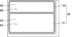
- a seal 50 surrounding the first liquid crystal layer 5A and surrounding the second liquid crystal layer 5B may be formed.
- the seal 50 corresponds to the first seal described above, and includes a first seal portion 51 surrounding the first liquid crystal layer 5A, and a second seal portion 52 corresponding to the second seal described above and surrounding the second liquid crystal layer 5B. Contains.
- a part of the seal 50 that is disposed at the boundary between the transmission part 6B and the image display part 6A is adjacent to both the first and second liquid crystal layers 5A and 5B.
- the transmissive liquid crystal display device has been described.
- the liquid crystal display panel of each liquid crystal display device may be a reflective or transflective liquid crystal display device and reflects external light.
- a reflective display unit that performs display may be provided.
- liquid crystal display device 2 liquid crystal display panel 3: array substrate 4: counter substrate 5A: first liquid crystal layer 5B: second liquid crystal layer 6A: video display unit 6B: transmission unit 6C: light shielding unit 7: pixel 8: scanning line 9: Signal line 10: Thin film transistor (TFT) 10G: gate electrode 10S: source electrode 10D: drain electrode 11: pixel electrode 12: counter electrode 13, 14: polarizing plate 13A, 14A: polarizing plate opening 15: bezel cover 16: backlight 16A: backlight opening 17: Driver circuit 18: Printed circuit board 20: Light source 21: Light guide plate 21A: Light guide plate opening 22: Cold cathode tube 23: Lamp reflectors 24 to 26: Optical sheets 24A to 26A: Optical sheet opening 30: Frame 30A: Frame opening 31, 41: Insulating substrate 32, 44: Alignment film 42: Black matrix (BM) 43: light shielding film 45: color filter layer 45R: red color filter 45G: green color filter 45B: blue color filter 50: seal 51: first seal
Landscapes
- Physics & Mathematics (AREA)
- Nonlinear Science (AREA)
- Mathematical Physics (AREA)
- Chemical & Material Sciences (AREA)
- Crystallography & Structural Chemistry (AREA)
- General Physics & Mathematics (AREA)
- Optics & Photonics (AREA)
- Spectroscopy & Molecular Physics (AREA)
- Liquid Crystal (AREA)
Abstract
Description
前記液晶表示パネルは、前記液晶表示パネルの後方の視認が可能な透過部と、
複数の画素を含み、映像の表示が可能な映像表示部と、
前記映像表示部に対応して設けられた第一液晶層と、
前記透過部に対応して設けられた第二液晶層と、
前記第二液晶層を囲むシールとを含んでもよく、
前記第一液晶層及び前記第二液晶層は、前記シールによって隔てられてもよい。
以下、この液晶表示装置を本発明に係る液晶表示装置とも言う。
前記一対の基板は各々、前記映像表示部及び前記透過部に設けられた配向膜を含んでもよく、
前記配向膜は、前記映像表示部及び前記透過部において同じように配向処理が施されているか、又は、前記映像表示部及び前記透過部おいて配向処理が施されていなくてもよい。
前記透過部に設けられた複数の第二スペーサとを含んでもよく、
前記複数の第二スペーサの配置密度及び/又は接触面積は、それぞれ、前記複数の第一スペーサの配置密度及び/又は接触面積よりも小さくてもよい。
前記映像表示部に設けられた第一スペーサと、
前記透過部に設けられた第二スペーサとを含んでもよく、
前記一対の基板の少なくとも一方は、絶縁基板と、前記絶縁基板及び前記第一スペーサの間に設けられた構成部材とを含んでもよく、前記絶縁基板及び前記第二スペーサの間には前記構成部材と同じ材料から形成された構成部材を含まなくてもよい。
前記一対の基板の少なくとも一方の構造は、前記映像表示部及び前記透過部の間で互いに異なってもよい。
前記カラーフィルタ層、前記ブラックマトリクス及び前記対向電極の前記少なくとも一つは、前記透過部に設けられずに前記映像表示部に設けられてもよい。
前記一対の偏光板の少なくとも一方は、前記透過部に重ならず、かつ、前記映像表示部に重なるように設けられてもよい。
図1は、実施形態1の液晶表示装置の斜視分解模式図である。図2は、実施形態1の液晶表示装置に含まれる液晶表示パネルの平面模式図である。図3は、実施形態1の液晶表示装置に含まれる液晶表示パネルの断面模式図である。
すなわち、第二液晶層5B用の液晶材料は、第一液晶層5A用の液晶材料と異なっていてもよいが、同じであることが好ましい。また、第二液晶層5Bの液晶は、第一液晶層5Aの液晶と同様に配向していることが好ましい。第二液晶層5Bの配向状態は、第一液晶層5Aの配向状態と異なっていてもよいが、第二液晶層5Bの液晶は、第一液晶層5Aの液晶と同様に配向していることが好ましく、各配向膜32、44は、第一及び第二液晶層5A及び5Bの液晶を同様に配向させることが好ましい。第一及び第二液晶層5A及び5Bの配向状態としては、例えば、ツイスト配向、垂直配向、水平配向等が挙げられる。各配向膜32、44に配向処理が必要であれば、各配向膜32、44は、映像表示部6A及び透過部6Bで同じように配向処理が施されていることが好ましい。配向処理としては、例えば、ラビング処理、光配向処理等が挙げられる。このとき、各配向膜32、44は、映像表示部6A及び透過部6Bで同じ条件で配向処理が施されていることが好ましい。各配向膜32、44に配向処理が必要ない場合、例えば、各配向膜32、44が配向処理されなくとも液晶を垂直に配向させる垂直配向膜である場合は、各配向膜32、44は、映像表示部6A及び透過部6Bで配向処理されていないことが好ましい。各配向膜32、44に対して配向処理を施すか否かについては、液晶表示パネル2の表示モードに応じて適宜、決定することができる。液晶表示パネル2の表示モードとしては、例えば、TN(Twisted Nematic)モード、VA(Vertical Alignment)モード、IPS(In-Plane Switching)モード、FFS(Fringe Field Switching)モード等が挙げられる。
図4に示すように、バックライト16は、一対の光源部20、導光板21、光学シート24~26、フレーム30等の構成部材を備えている。各光源部20は、光源としての冷陰極管22と、ランプリフレクタ23とを備えている。冷陰極管22は、略矩形状の導光板21の長手方向に延在する細長い円筒状の光源である。ランプリフレクタ23は、冷陰極管22から放射された光を導光板21に向けて反射するものであり、冷陰極管22の周囲を取り囲むように配置されている。
本実施形態は、アレイ基板及び対向基板の透過部におけるパターンが異なることを除いて、実施形態1と実質的に同じである。したがって、本実施形態では、本実施形態に特有の特徴について主に説明し、実施形態1と重複する内容については説明を省略する。また、本実施形態と実施形態1とにおいて、同一又は同様の機能を有する部材には同一の符号を付し、本実施形態において、その部材の説明は省略する。
図6は、実施形態2の液晶表示装置に含まれる液晶表示パネルの断面模式図である。図7は、実施形態2の液晶表示装置に含まれる液晶表示パネルの平面模式図である。
本実施形態は、スペーサの配置部分における構造が異なることを除いて、実施形態1と実質的に同じである。したがって、本実施形態では、本実施形態に特有の特徴について主に説明し、実施形態1と重複する内容については説明を省略する。また、本実施形態と実施形態1とにおいて、同一又は同様の機能を有する部材には同一の符号を付し、本実施形態において、その部材の説明は省略する。
図8及び9は、実施形態3の液晶表示装置に含まれる液晶表示パネルの断面模式図である。
本比較形態の液晶表示装置に含まれる液晶表示パネルでは、透過部においてアレイ基板及び対向基板の間に、第二液晶層の代わりにシール材が充填されている。しかしながら、シール材の材料設計は、光学特性を考慮して行われていないため、シール材の透過率は非常に低い。また、シール材の屈折率は、ガラスの屈折率に合うように考慮されていないため、透過部の透過率が大幅に低下する。更に、シール材をアレイ基板又は対向基板上に描画した後、アレイ基板と対向基板でシール材を挟んで加圧し、セル厚に見合ったシールの厚みを決定するが、透過部の全域に配置されたシール材と、通常幅のシール材(例えば対向基板の端部に沿って配置されたシール材)とでは、加圧の際の圧縮され方が違う(透過部のシール材は圧縮されたり広がったりしにくい)ため、セル厚ムラが発生する。
本比較形態の液晶表示装置に含まれる液晶表示パネルでは、透過部においてアレイ基板及び対向基板の間に、第二液晶層の代わりにスペーサ材が充填されている。しかしながら、スペーサ材の材料設計は、光学特性を考慮して行われていないため、スペーサ材の透過率は非常に低い。また、スペーサ材の屈折率は、ガラスの屈折率に合うように考慮されていないため、透過部の透過率が大幅に低下する。更に、映像表示部のスペーサの径と、透過部にスペーサ材を充填して形成されたスペーサの径とが互いに大きく異なるため、アレイ基板と対向基板を貼り合せた際に、映像表示部と透過部との間でスペーサの厚みの圧縮のされ方が異なり、セル厚ムラが発生する。なお、この圧縮率の差をあらかじめ見越して、映像表示部と透過部とでスペーサの高さを互いに異ならせることも考えられるが、このためには、スペーサ形成工程に余分な工程を追加する必要が生じる。
本比較形態の液晶表示装置に含まれる液晶表示パネルは、透過部においてアレイ基板及び対向基板の間に、第二液晶層の代わりに特別に用意した材料が充填されている。しかしながら、通常のパネル製造工程では使用しない材料(光学特性と、セル厚ムラが発生しないように粘度とを考慮した材料)を導入する必要があり、液晶の滴下注入工程とは別に、この材料を充填する工程が必要になる。
図10~12は、実施形態1~3の液晶表示装置に含まれる液晶表示パネルの変形例の平面模式図である。
2:液晶表示パネル
3:アレイ基板
4:対向基板
5A:第一液晶層
5B:第二液晶層
6A:映像表示部
6B:透過部
6C:遮光部
7:画素
8:走査線
9:信号線
10:薄膜トランジスタ(TFT)
10G:ゲート電極
10S:ソース電極
10D:ドレイン電極
11:画素電極
12:対向電極
13、14:偏光板
13A、14A:偏光板の開口部
15:ベゼルカバー
16:バックライト
16A:バックライトの開口部
17:ドライバ回路
18:プリント配線基板
20:光源部
21:導光板
21A:導光板の開口部
22:冷陰極管
23:ランプリフレクタ
24~26:光学シート
24A~26A:光学シートの開口部
30:フレーム
30A:フレームの開口部
31、41:絶縁基板
32、44:配向膜
42:ブラックマトリクス(BM)
43:遮光膜
45:カラーフィルタ層
45R:赤色カラーフィルタ
45G:緑色カラーフィルタ
45B:青色カラーフィルタ
50:シール
51:第一シール(第一シール部分)
52:第二シール(第二シール部分)
53:第一スペーサ
54:第二スペーサ
60:筐体
61:窓部
62:保護板
70:回転リール
71:リール本体
208:信号用配線
208A:配線
208B:配線
Claims (10)
- 液晶表示パネルを備える液晶表示装置であって、
前記液晶表示パネルは、前記液晶表示パネルの後方の視認が可能な透過部と、
複数の画素を含み、映像の表示が可能な映像表示部と、
前記映像表示部に対応して設けられた第一液晶層と、
前記透過部に対応して設けられた第二液晶層と、
前記第二液晶層を囲むシールとを含み、
前記第一液晶層及び前記第二液晶層は、前記シールによって隔てられる液晶表示装置。 - 前記第二液晶層は、配向していない液晶を含む請求項1記載の液晶表示装置。
- 前記第二液晶層は、配向した液晶を含む請求項1記載の液晶表示装置。
- 前記液晶表示パネルは、前記第一液晶層及び前記第二液晶層を挟持する一対の基板を含み、
前記一対の基板は各々、前記映像表示部及び前記透過部に設けられた配向膜を含み、
前記配向膜は、前記映像表示部及び前記透過部において同じように配向処理が施されているか、又は、前記映像表示部及び前記透過部おいて配向処理が施されていない請求項3記載の液晶表示装置。 - 前記液晶表示パネルは、前記映像表示部に設けられた複数の第一スペーサと、
前記透過部に設けられた複数の第二スペーサとを含み、
前記複数の第二スペーサの配置密度及び/又は接触面積は、それぞれ、前記複数の第一スペーサの配置密度及び/又は接触面積よりも小さい請求項1~4のいずれかに記載の液晶表示装置。 - 前記液晶表示パネルは、前記第一液晶層及び前記第二液晶層を挟持する一対の基板と、
前記映像表示部に設けられた第一スペーサと、
前記透過部に設けられた第二スペーサとを含み、
前記一対の基板の少なくとも一方は、絶縁基板と、前記絶縁基板及び前記第一スペーサの間に設けられた構成部材とを含み、前記絶縁基板及び前記第二スペーサの間には前記構成部材と同じ材料から形成された構成部材を含まない請求項1~5のいずれかに記載の液晶表示装置。 - 前記液晶表示パネルは、前記第一液晶層及び前記第二液晶層を挟持する一対の基板を含み、
前記一対の基板の少なくとも一方の構造は、前記映像表示部及び前記透過部の間で互いに異なる請求項1~6のいずれかに記載の液晶表示装置。 - 前記一対の基板の一方は、カラーフィルタ層、ブラックマトリクス及び対向電極の少なくとも一つを含み、
前記カラーフィルタ層、前記ブラックマトリクス及び前記対向電極の前記少なくとも一つは、前記透過部に設けられずに前記映像表示部に設けられる請求項7記載の液晶表示装置。 - 前記液晶表示装置は、前記液晶表示パネルの前面及び背面上にそれぞれ設けられた一対の偏光板を備え、
前記一対の偏光板の少なくとも一方は、前記透過部に重ならず、かつ、前記映像表示部に重なるように設けられる請求項1~8のいずれかに記載の液晶表示装置。 - 前記一対の偏光板の両方は、前記透過部に重ならず、かつ、前記映像表示部に重なるように設けられる請求項9記載の液晶表示装置。
Priority Applications (2)
| Application Number | Priority Date | Filing Date | Title |
|---|---|---|---|
| US14/917,956 US9720287B2 (en) | 2013-09-24 | 2014-08-22 | Liquid crystal display device |
| JP2015539021A JP6235600B2 (ja) | 2013-09-24 | 2014-08-22 | 液晶表示装置 |
Applications Claiming Priority (2)
| Application Number | Priority Date | Filing Date | Title |
|---|---|---|---|
| JP2013-197280 | 2013-09-24 | ||
| JP2013197280 | 2013-09-24 |
Publications (1)
| Publication Number | Publication Date |
|---|---|
| WO2015045694A1 true WO2015045694A1 (ja) | 2015-04-02 |
Family
ID=52742846
Family Applications (1)
| Application Number | Title | Priority Date | Filing Date |
|---|---|---|---|
| PCT/JP2014/071957 Ceased WO2015045694A1 (ja) | 2013-09-24 | 2014-08-22 | 液晶表示装置 |
Country Status (3)
| Country | Link |
|---|---|
| US (1) | US9720287B2 (ja) |
| JP (1) | JP6235600B2 (ja) |
| WO (1) | WO2015045694A1 (ja) |
Cited By (4)
| Publication number | Priority date | Publication date | Assignee | Title |
|---|---|---|---|---|
| WO2017077963A1 (ja) * | 2015-11-05 | 2017-05-11 | シャープ株式会社 | 液晶表示装置 |
| CN110062907A (zh) * | 2016-12-15 | 2019-07-26 | 夏普株式会社 | 显示装置 |
| JP2022514104A (ja) * | 2018-12-20 | 2022-02-09 | 華為技術有限公司 | 液晶ディスプレイ、電子デバイス、および液晶ディスプレイ製造方法 |
| JP2023067474A (ja) * | 2021-11-01 | 2023-05-16 | 株式会社ジャパンディスプレイ | 電子機器 |
Families Citing this family (4)
| Publication number | Priority date | Publication date | Assignee | Title |
|---|---|---|---|---|
| KR20160069628A (ko) * | 2014-12-08 | 2016-06-17 | 삼성디스플레이 주식회사 | 액정 표시 장치 |
| CN104765185B (zh) * | 2015-03-17 | 2018-05-15 | 业成光电(深圳)有限公司 | 液晶显示装置及其制作方法 |
| CN106054442B (zh) * | 2016-08-18 | 2019-04-09 | 京东方科技集团股份有限公司 | 显示面板及其盒厚测试方法、显示装置 |
| US20220052128A1 (en) * | 2018-09-10 | 2022-02-17 | Sharp Kabushiki Kaisha | Display device |
Citations (4)
| Publication number | Priority date | Publication date | Assignee | Title |
|---|---|---|---|---|
| JP2002116534A (ja) * | 2000-10-10 | 2002-04-19 | Dainippon Printing Co Ltd | 感光性樹脂組成物および液晶ディスプレイ用カラーフィルタ |
| JP2006343728A (ja) * | 2005-05-13 | 2006-12-21 | Toshiba Matsushita Display Technology Co Ltd | 液晶表示装置 |
| JP2007127940A (ja) * | 2005-11-07 | 2007-05-24 | Toshiba Matsushita Display Technology Co Ltd | 液晶表示装置 |
| JP2009139603A (ja) * | 2007-12-06 | 2009-06-25 | Hitachi Displays Ltd | 液晶表示装置およびその製造方法 |
Family Cites Families (8)
| Publication number | Priority date | Publication date | Assignee | Title |
|---|---|---|---|---|
| JPH09265087A (ja) | 1996-03-28 | 1997-10-07 | Nippon Seiki Co Ltd | 液晶表示装置 |
| JP2004105616A (ja) | 2002-09-20 | 2004-04-08 | Sanyo Electric Co Ltd | 表示器及びそれを備えた遊技機 |
| JP4456831B2 (ja) * | 2003-07-15 | 2010-04-28 | 株式会社 日立ディスプレイズ | スロットマシーン型遊技機 |
| JP2005052195A (ja) | 2003-08-04 | 2005-03-03 | Samii Kk | 回胴式遊技機 |
| JP2005052198A (ja) | 2003-08-04 | 2005-03-03 | Samii Kk | 回胴式遊技機 |
| JP2005052196A (ja) | 2003-08-04 | 2005-03-03 | Samii Kk | 回胴式遊技機 |
| JP4811502B2 (ja) * | 2009-07-01 | 2011-11-09 | カシオ計算機株式会社 | 液晶表示パネル及びタッチパネル |
| TWI554808B (zh) * | 2015-04-13 | 2016-10-21 | 友達光電股份有限公司 | 液晶顯示面板及液晶顯示器 |
-
2014
- 2014-08-22 JP JP2015539021A patent/JP6235600B2/ja not_active Expired - Fee Related
- 2014-08-22 WO PCT/JP2014/071957 patent/WO2015045694A1/ja not_active Ceased
- 2014-08-22 US US14/917,956 patent/US9720287B2/en not_active Expired - Fee Related
Patent Citations (4)
| Publication number | Priority date | Publication date | Assignee | Title |
|---|---|---|---|---|
| JP2002116534A (ja) * | 2000-10-10 | 2002-04-19 | Dainippon Printing Co Ltd | 感光性樹脂組成物および液晶ディスプレイ用カラーフィルタ |
| JP2006343728A (ja) * | 2005-05-13 | 2006-12-21 | Toshiba Matsushita Display Technology Co Ltd | 液晶表示装置 |
| JP2007127940A (ja) * | 2005-11-07 | 2007-05-24 | Toshiba Matsushita Display Technology Co Ltd | 液晶表示装置 |
| JP2009139603A (ja) * | 2007-12-06 | 2009-06-25 | Hitachi Displays Ltd | 液晶表示装置およびその製造方法 |
Cited By (10)
| Publication number | Priority date | Publication date | Assignee | Title |
|---|---|---|---|---|
| WO2017077963A1 (ja) * | 2015-11-05 | 2017-05-11 | シャープ株式会社 | 液晶表示装置 |
| CN108351552A (zh) * | 2015-11-05 | 2018-07-31 | 夏普株式会社 | 液晶显示装置 |
| CN108351552B (zh) * | 2015-11-05 | 2020-10-09 | 夏普株式会社 | 液晶显示装置 |
| CN110062907A (zh) * | 2016-12-15 | 2019-07-26 | 夏普株式会社 | 显示装置 |
| CN110062907B (zh) * | 2016-12-15 | 2021-12-21 | 夏普株式会社 | 显示装置 |
| JP2022514104A (ja) * | 2018-12-20 | 2022-02-09 | 華為技術有限公司 | 液晶ディスプレイ、電子デバイス、および液晶ディスプレイ製造方法 |
| JP7089641B2 (ja) | 2018-12-20 | 2022-06-22 | 華為技術有限公司 | 液晶ディスプレイ、電子デバイス、および液晶ディスプレイ製造方法 |
| US11796852B2 (en) | 2018-12-20 | 2023-10-24 | Huawei Technologies Co., Ltd. | Liquid crystal display, electronic device, and liquid crystal display manufacturing method |
| JP2023067474A (ja) * | 2021-11-01 | 2023-05-16 | 株式会社ジャパンディスプレイ | 電子機器 |
| JP7725339B2 (ja) | 2021-11-01 | 2025-08-19 | 株式会社Magnolia White | 電子機器 |
Also Published As
| Publication number | Publication date |
|---|---|
| JPWO2015045694A1 (ja) | 2017-03-09 |
| JP6235600B2 (ja) | 2017-11-22 |
| US20160216542A1 (en) | 2016-07-28 |
| US9720287B2 (en) | 2017-08-01 |
Similar Documents
| Publication | Publication Date | Title |
|---|---|---|
| JP6235600B2 (ja) | 液晶表示装置 | |
| KR100975184B1 (ko) | 액정 표시 장치 | |
| JP6240612B2 (ja) | 液晶表示装置 | |
| US8013961B2 (en) | Liquid crystal display device | |
| US9291851B2 (en) | Display and electronic unit | |
| CN110596928A (zh) | 显示装置 | |
| JP3692445B2 (ja) | 液晶装置及び電子機器 | |
| JP2007148279A (ja) | 表示装置 | |
| EP2293138A1 (en) | Liquid crystal display apparatus | |
| KR20160088397A (ko) | 헤드업 디스플레이 장치용 액정 표시 장치 및 헤드업 디스플레이 장치 | |
| CN107945760B (zh) | 液晶显示面板及其驱动方法、显示装置 | |
| CN103995390B (zh) | 显示面板、显示装置及显示面板的制造方法 | |
| CN101484846A (zh) | 显示装置 | |
| US20060262253A1 (en) | Liquid crystal display device | |
| JP2007017798A (ja) | 液晶表示装置 | |
| TWI635335B (zh) | Display device | |
| CN201903700U (zh) | 采用视差挡板法的显示装置 | |
| WO2012046725A1 (ja) | 表示パネル及びそれを備えた表示装置 | |
| JP2007140089A (ja) | 液晶表示装置 | |
| CN101960365A (zh) | 液晶显示装置 | |
| JP2007304436A (ja) | 表示装置、偏光素子、防眩性フィルム、及び、その製造方法 | |
| US20210232006A1 (en) | Display panel and display device | |
| EP3432063A1 (en) | Display apparatus | |
| KR102123947B1 (ko) | 멀티패널 표시장치 | |
| JP2024166827A (ja) | 液晶表示装置 |
Legal Events
| Date | Code | Title | Description |
|---|---|---|---|
| 121 | Ep: the epo has been informed by wipo that ep was designated in this application |
Ref document number: 14848686 Country of ref document: EP Kind code of ref document: A1 |
|
| ENP | Entry into the national phase |
Ref document number: 2015539021 Country of ref document: JP Kind code of ref document: A |
|
| WWE | Wipo information: entry into national phase |
Ref document number: 14917956 Country of ref document: US |
|
| NENP | Non-entry into the national phase |
Ref country code: DE |
|
| 122 | Ep: pct application non-entry in european phase |
Ref document number: 14848686 Country of ref document: EP Kind code of ref document: A1 |