WO2015033489A1 - 表示装置 - Google Patents
表示装置 Download PDFInfo
- Publication number
- WO2015033489A1 WO2015033489A1 PCT/JP2014/002167 JP2014002167W WO2015033489A1 WO 2015033489 A1 WO2015033489 A1 WO 2015033489A1 JP 2014002167 W JP2014002167 W JP 2014002167W WO 2015033489 A1 WO2015033489 A1 WO 2015033489A1
- Authority
- WO
- WIPO (PCT)
- Prior art keywords
- chassis
- chassis member
- display panel
- display device
- recess
- Prior art date
- Legal status (The legal status is an assumption and is not a legal conclusion. Google has not performed a legal analysis and makes no representation as to the accuracy of the status listed.)
- Ceased
Links
Images






Classifications
-
- H—ELECTRICITY
- H04—ELECTRIC COMMUNICATION TECHNIQUE
- H04N—PICTORIAL COMMUNICATION, e.g. TELEVISION
- H04N5/00—Details of television systems
- H04N5/64—Constructional details of receivers, e.g. cabinets or dust covers
Definitions
- the present disclosure relates to a display device including a display panel.
- a display device having a thin display panel such as a liquid crystal display device or an organic EL (Electro Luminescence) display device
- the rigidity of the display panel is secured by arranging a metal chassis on the back side of the display panel.
- Patent Document 1 When it is difficult to ensure the rigidity of the display panel with a flat chassis, it is known to reinforce the chassis by providing a diaphragm in the chassis (Patent Document 1).
- the present disclosure has been made in view of such a problem, and an object thereof is to provide a display device including a chassis structure having a desired strength.
- a display device includes a display panel and a chassis structure that holds the display panel, and the chassis structure is formed with a recess so as to have an opening on the display panel side.
- the chassis structure having the desired strength is provided, the desired rigidity of the display panel can be ensured even with a thin chassis structure. Thereby, a thin display panel having excellent rigidity can be realized. Furthermore, the heat dissipation of the display panel can be improved.
- FIG. 1 is an external perspective view of the display device according to the first embodiment.
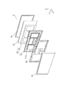
- FIG. 2 is an exploded perspective view of the display device according to the first embodiment.
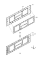
- FIG. 3 is a view showing a state when the chassis structure in the first embodiment is assembled, (a) shows a state before the first chassis member and the second chassis member are joined, (B) has shown the state after joining the 1st chassis member and the 2nd chassis member.
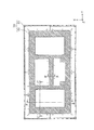
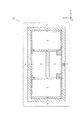
- FIG. 4 is a plan view of the chassis structure according to the first embodiment.
- FIG. 5 is a plan view of the chassis structure shown in FIG. 4 as seen through the second chassis member.
- FIG. 6 is a plan view schematically showing the region of the step portion of the first chassis member in the first embodiment.
- FIG. 7A is a cross-sectional view of the chassis structure and the display panel corresponding to a cross section taken along line A-A ′ of FIGS. 4 and 5.
- FIG. 7B is a cross-sectional view of the chassis structure and the display panel corresponding to a cross section taken along the line B-B ′ of FIGS. 4 and 5.
- FIG. 7C is a cross-sectional view of the chassis structure and the display panel corresponding to a cross section taken along line C-C ′ of FIGS. 4 and 5.
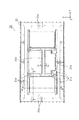
- FIG. 8 is a plan view showing the configuration of the first chassis member in the display device according to the second embodiment.
- FIG. 9 is an enlarged view of a region X surrounded by a broken line in FIG. FIG.
- FIG. 10 is a cross-sectional view of the chassis structure and the display panel corresponding to a cross section taken along the line D-D ′ of FIG. 8.
- FIG. 11 is a cross-sectional view of the chassis structure and the display panel in the display device according to the first modification.
- FIG. 12 is a cross-sectional view of a chassis structure and a display panel in a display device according to Modification 2.
- FIG. 13 is a cross-sectional view of the chassis structure and the display panel in the display device according to the third modification.
- FIG. 1 is an external perspective view of the display device according to the first embodiment.
- FIG. 2 is an exploded perspective view of the display device according to the first embodiment.
- the display device 1 includes a display panel 10 for displaying an image and a chassis structure 20 that holds the display panel 10.
- the display device 1 further includes a rectangular frame (frame) 30 that covers the periphery of the display-side surface of the display panel 10 and a back cover (back housing) 40 that covers the entire chassis structure 20.
- the frame 30 and the back cover 40 are formed using, for example, a resin material or a metal material.
- the display device 1 has a structure in which the display panel 10 and the chassis structure 20 are disposed between the frame 30 and the back cover 40.
- a display device 1 is, for example, a television receiver that outputs a video signal and an audio signal obtained from a received broadcast wave or the like.
- the display panel 10 is, for example, an organic EL (Electro Luminescence) panel, and the thickness thereof is, for example, about 1 mm to 3 mm.
- the display panel 10 is not limited to an organic EL panel, and may be other flat panel display devices such as an inorganic EL panel, a plasma display panel, or a liquid crystal display panel.
- the display panel 10 is attached to the front surface of the chassis structure 20.
- a plurality of circuit boards 50 are attached to the back surface of the chassis structure 20.
- the circuit board 50 is a PCB (Printed Circuit Board) on which a plurality of circuit components are mounted.
- the circuit board 50 is a drive circuit board provided with a drive circuit (driver) that supplies a signal voltage to the display panel 10.
- the circuit board 50 is disposed along the periphery of the chassis structure 20 and is connected to the display panel 10 via a flexible cable.
- a driver IC may be mounted on the flexible cable.
- a power supply circuit board etc. which are arrange
- the chassis structure 20 is, for example, a metal rigid body, and includes two members, a first chassis member 21 having a recess 21a and a plate-like second chassis member 22.
- the first chassis member 21 is a metal rectangular plate member (metal plate) made of, for example, aluminum or iron, and the plate member is subjected to pressing such as drawing so that the concave portion 21a is formed. It is the chassis main body shape
- the recess 21a of the first chassis member 21 is formed to have an opening on the display panel 10 side by this pressing.
- the recess 21a having an opening can be formed by drawing an aluminum plate having a thickness of 0.6 mm. In this way, the first chassis member 21 can be reinforced and the rigidity can be increased by forming the recess 21a (diaphragm).
- the second chassis member 22 is obtained by processing a metal plate member (metal plate) made of, for example, aluminum or iron into a predetermined shape, and at least a part of the opening of the recess 21a of the first chassis member 21 is formed. It attaches to the 1st chassis member 21 so that it may block. That is, the second chassis member 22 is attached to the first chassis member 21 so as to straddle the opening of the recess 21 a of the first chassis member 21.
- the second chassis member 22 is an aluminum plate having a thickness of 0.6 mm, and is formed in a predetermined shape so as to close all the openings of the recesses 21 a of the first chassis member 21.
- the second chassis member 22 is arranged on the first chassis member 21 so that the surface of the second chassis member 22 faces the back surface of the display panel 10.
- FIG. 3 is a view showing a state when the chassis structure in the first embodiment is assembled, (a) shows a state before the first chassis member and the second chassis member are joined, (B) has shown the state after joining the 1st chassis member and the 2nd chassis member.
- the second chassis member 22 is hatched for easy understanding of the second chassis member 22.
- the second chassis member 22 is disposed on the first chassis member 21 so as to close the opening of the concave portion 21a of the first chassis member 21, for example, caulking.
- the second chassis member 22 and the first chassis member 21 are joined together.
- the chassis structure 20 in which the first chassis member 21 and the second chassis member 22 are integrated is obtained.
- first chassis member 21 and the second chassis member 22 may be joined by other joining methods such as spot welding and screwing instead of caulking.
- the first chassis member 21 can be reinforced by disposing the second chassis member 22 so as to close the opening of the recess 21a of the first chassis member 21.
- the chassis structure 20 having a strength necessary for holding the display panel 10 can be obtained while using a thin material as the material. Therefore, even when the length of the first chassis member 21 in the depth direction after forming the recess 21a is small and the chassis structure 20 has a thin structure, a desired rigidity capable of holding the display panel 10 can be obtained.
- the display panel 10 side as the chassis structure 20 is compared with the case where the second chassis member 22 is not used.
- the surface of can be brought close to a flat shape.
- chassis structure 20 will be described with reference to FIGS. 4 to 6 and FIGS. 7A to 7C.
- FIG. 4 is a plan view of the chassis structure in the first embodiment
- FIG. 5 is a plan view of the chassis structure shown in FIG. 4 viewed through the second chassis member
- FIG. 6 is a plan view schematically showing the region of the step portion of the first chassis member in the first embodiment.
- 7A, 7B, and 7C are chassis corresponding to the cross sections taken along lines AA ′, BB ′, and CC ′, respectively, in FIGS. 4 and 5, respectively. It is sectional drawing of a structure and a display panel.
- the recess 21a is formed by drawing so as to have a plurality of step portions. That is, the recess 21a is a stop, and is a stepped portion formed in a step shape so that a predetermined region of the first chassis member 21 rises (projects).
- the concave portion 21a is formed by raising the surface of the first chassis member 21 on the back cover 40 side (surface opposite to the display panel 10 side).
- a step portion is formed by forming the recess 21a.
- the depth of the recess 21a (the depth of the diaphragm) can be set to 0.5 mm to 10 mm, for example.
- the recess 21a has a four-stage drawing, and is drawn so as to have four steps.
- areas indicated as “0” to “4” indicate the depth positions of the steps, and the areas indicating the step portions at the same depth positions are provided with the same hatching.
- an area illustrated as “0” is an area that serves as a reference surface and is not subjected to drawing.
- the region illustrated as “0” is a region closest to the display panel 10 and is a portion that is in contact with or connected to the display panel 10.
- the region illustrated as “1” is a region that is one step deeper than the reference surface
- the region illustrated as “2” is a region that is two steps deeper than the reference surface, and is illustrated as “3”.
- the region indicated is a region that is three steps deep from the reference plane
- the region indicated as “4” is a region that is four steps deep from the reference plane.
- the recessed part 21a in this Embodiment is drawn so that it may have a several level
- the second chassis member 22 is shaped so as to block only the opening of the recess 21a of the first chassis member 21. As shown in FIG. Specifically, the second chassis member 22 is formed so as to have an opening (through hole) only in the region “0” in FIG. 6, and the region other than the region “0” in FIG. , “1” to “4”) have plate members.
- the weight can be reduced compared to a plate member in which no opening is formed. Therefore, even if it uses the 2nd chassis member 22, the weight increase of the chassis structure 20 can be suppressed. Therefore, the thin chassis structure 20 having a desired strength and reduced in weight can be obtained.
- the second chassis member 22 is arranged at one step portion among the plurality of step portions of the recess 21a of the first chassis member 21.
- the length in the depth direction of the chassis structure 20 can be reduced.
- the structure 20 can be obtained.
- the second chassis member 22 is attached to the first chassis member 21 by setting the plate thickness of the second chassis member 22 to be equal to or less than the depth of the step portion where the second chassis member 22 is disposed.
- the length of the chassis structure 20 in the depth direction can be the length of the first chassis member 21 in the depth direction. That is, the thickness of the second chassis member 22 can be absorbed by the step portion of the first chassis member 21.
- the 2nd chassis member 22 when joining the some location of the 1st chassis member 21 and the 2nd chassis member 22 by caulking, the 2nd chassis member 22 will shift
- the depth of the stepped portion of the first chassis member 21 for arranging the second chassis member 22 may be determined in consideration of the plate thickness of the second chassis member 22 and the variation in caulking.
- chassis structure 20 also functions as a heat capacity member that absorbs and dissipates heat generated in the display panel 10, the positional relationship between the first chassis member 21 and the second chassis member 22 or the recess 21a. It is also desirable to take this point of view into consideration when determining the region that closes the opening.
- the second chassis member 22 is disposed at a step portion formed at a position closest to the display panel 10 among the plurality of step portions of the recess 21a. That is, the second chassis member 22 is disposed on the first chassis member 21 so as to be in contact with the bottom of the first step portion which is the region “1” in FIG. 6.
- the second chassis member 22 as a plate member can be brought close to the display panel 10, the surface of the chassis structure 20 on the display panel 10 side can be formed in a flat shape. Therefore, the heat generated in the display panel 10 can be efficiently absorbed and radiated by the chassis structure 20.
- the second chassis member 22 is disposed on the first chassis member 21 so as to block all the openings of the recesses 21a. Specifically, the second chassis member 22 is disposed so as to cover an area other than the area “0” in FIG. 6 (that is, the area “1” to the area “4”).
- the entire surface of the chassis structure 20 on the display panel 10 side can be configured to be flat so as to cover the entire display panel 10, so that the entire rear surface of the display panel 10 is configured to be a flat display panel of the chassis structure 20. Can be covered with side surfaces. Therefore, the heat-dissipating effect of heat generated in the display panel 10 by the chassis structure 20 can be improved, so that the heat dissipation of the display panel 10 can be further improved.
- the second chassis member 22 has a stepped portion so that the surface of the peripheral portion of the first chassis member 21 and the surface of the second chassis member 22 are flush with each other. Is arranged. Specifically, the plate thickness of the second chassis member 22 is configured to be substantially the same as the depth of the step portion in the “1” region of the recess 21 a of the first chassis member 21.
- the depth of the concave portion 21a (the depth of the diaphragm) in the first step portion which is the region “1” in FIG. about 6 mm.
- the depth (throttle depth) of the second to fourth recesses 21a can be set to, for example, about 7 mm.
- the entire surface of the chassis structure 20 on the display panel 10 side can be made substantially flat, so that the entire back surface of the display panel 10 and the entire surface of the chassis structure 20 on the display panel side can be brought into contact with each other. Can do. That is, the entire surface (contact surface) where the display panel 10 and the chassis structure 20 face each other can be made a substantially uniform plane. Therefore, the heat generated in the display panel 10 can be uniformly absorbed by the chassis structure 20 over the entire back surface of the display panel 10, so that the heat uniformity of the display panel 10 can be further improved.
- the display panel 10 and the chassis structure 20 are bonded to each other by an adhesive member 60 such as a double-sided tape or a double-sided pressure-sensitive adhesive sheet.
- an adhesive member 60 such as a double-sided tape or a double-sided pressure-sensitive adhesive sheet.
- a double-sided tape having a thickness of 0.03 mm is attached as the adhesive member 60 between the peripheral portion on the back surface of the display panel 10 and the peripheral portion of the first chassis member 21.
- the chassis structure 20 configured to close the concave portion 21a of the first chassis member 21 with the plate-like second chassis member 22 is used.
- the display panel 10 can be held even if the first chassis member 21 is a thin and thin chassis structure 20.
- the chassis structure 20 having the necessary strength is obtained. Therefore, since the desired rigidity of the display panel 10 can be ensured, a thin display device with excellent rigidity can be realized.
- the recess 21a is closed by the second chassis member 22 which is a plate member, the surface of the chassis structure 20 on the display panel 10 side can be configured to be substantially planar.
- the heat generated in the display panel 10 can be efficiently absorbed by the chassis structure 20, so that the heat dissipation of the display panel 10 can be improved.
- the heat dissipation of the display panel 10 can be improved while ensuring the desired rigidity of the display panel 10.
- the structure in which the plate-like second chassis member 22 covers all the openings of the recesses 21a of the first chassis member 21 is exemplified.
- the present invention is not limited to this structure. What is necessary is just to determine the area
- the structure having one recess 21a is illustrated, but the present invention is not limited to this structure, and the first chassis member 21 may be provided with a plurality of recesses 21a.
- the second chassis member 22 may be configured so as to block all the openings of the plurality of recesses 21a, but at least one of the plurality of recesses 21a in view of the required strength. What is necessary is just to comprise so that the opening of the one recessed part 21a may be plugged up.
- the region for closing the opening of the concave portion 21a may be determined based on the required strength as described above, and the regions to be closed may be the same or different depending on the opening.
- you may comprise the 2nd chassis member 22 by two or more.
- FIG. 8 is a plan view showing the configuration of the first chassis member in the display device according to the second embodiment.
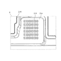
- FIG. 9 is an enlarged view of a region X surrounded by a broken line in FIG.
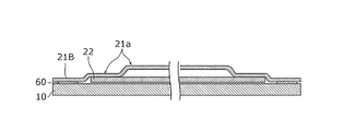
- FIG. 10 is a cross-sectional view of the chassis structure and the display panel corresponding to a cross section taken along line DD ′ of FIG.
- a plurality of through holes (holes) 21b are provided at the bottom of the recess 21a of the first chassis member 21A in the chassis structure 20A. ing.
- the first chassis member 21A in the present embodiment has the same configuration as that of the first chassis member 21 in the first embodiment except that the through hole 21b is provided.
- the second chassis member 22 in the first embodiment is used.
- the second chassis member 22 is a recess 21a of the first chassis member 21A. It is attached to the first chassis member 21A so as to close the opening.
- the through holes 21b in the first chassis member 21A do not need to be provided on the entire bottom surface of the recess 21a, but may be provided only on the bottom surface of the required region.
- the through holes 21b are provided at four bottoms of the stepped portion of the region “3” among the stepped portions of the recess 21a. At each location, a plurality of through holes 21b are provided in a matrix.
- one through hole 21 b and the other through hole 21 b of the plurality of through holes 21 b are recessed portions 21 a surrounded by the first chassis member 21 ⁇ / b> A and the second chassis member 22. It is connected through the space area.
- the plurality of through holes 21b are all spatially connected to each other through the space area of one recess 21a.
- the same effect as the display device 1 in the first embodiment can be obtained. That is, since the desired rigidity of the display panel 10 can be secured even with the thin chassis structure 20A, a thin display device with excellent rigidity can be realized. Furthermore, the heat dissipation of the display panel 10 can be improved.
- the heat dissipation of the chassis structure 20A can be further improved. .
- the chassis structure 20 having a structure in which the concave portion 21a of the first chassis member 21 is closed with the plate-like second chassis member 22 as in the first embodiment, heat from the display panel 10 is generated by the chassis structure. After being transmitted to the body 20, it is desirable that heat is quickly dissipated. However, if there is a space area of the recess 21 a surrounded by the first chassis member 21 and the second chassis member 22, the space area is sealed. Since the ventilation is delayed, the heat transmitted to the chassis structure 20 is not efficiently dissipated, and the thermal uniformity of the display panel 10 may be reduced.
- the recess 21a of the first chassis member 21A is replaced by the second chassis member 22.
- the ventilation in the space region of the recess 21a surrounded by the first chassis member 21A and the second chassis member 22 is so-called chimney effect. Can be performed through the through hole 21b.
- the heat transmitted from the display panel 10 to the chassis structure 20A can be efficiently dissipated, so that the heat uniformity of the display panel 10 can be prevented from being lowered.
- the first chassis member 21A can be reduced in weight by providing the first chassis member 21A with the through hole 21b. As a result, a thin chassis structure 20A having a desired strength and reduced in weight can be obtained.
- the through hole 21b can also be formed on the side surface of the recess 21a (the side surface of the stepped portion).
- the through-hole 21b is preferably formed on the bottom surface of the recess 21a rather than the side surface of the recess 21a.
- the recesses 21a of the first chassis members 21 and 21A have been drawn so as to have four stepped portions, but are not limited to this structure.
- the first chassis member 21B may be configured such that the recess 21a has two step portions.
- the second chassis member 22 is disposed at the stepped portion of the first chassis members 21 and 21A, but the present invention is not limited to this structure.
- the second chassis member 22 may be disposed in a portion where the step portion of the first chassis member 21B is not formed.
- the adhesive member 60 is provided between the peripheral edge of the display panel 10 and the peripheral edge of the second chassis member 22.
- the recesses 21a of the first chassis members 21 and 21A have been drawn so as to have a plurality of stepped portions, but the present invention is not limited to this structure.
- the recess 21a has one step portion.
- the first chassis member 21C may be configured.
- the display device is a television receiver.
- the present invention is not limited to this.
- the display device is a monitor display that displays video input from the outside, a digital signage used as an advertising medium, or a mobile terminal, a tablet terminal, or a table-type display device that receives a user operation through a touch panel. Also good.
- the present disclosure is useful for display devices that are required to be thin, for example, and can be applied to electronic devices such as a television receiver, a monitor display, a digital signage, a portable terminal, a tablet terminal, or a table-type display device.
Landscapes
- Engineering & Computer Science (AREA)
- Multimedia (AREA)
- Signal Processing (AREA)
- Devices For Indicating Variable Information By Combining Individual Elements (AREA)
- Microelectronics & Electronic Packaging (AREA)
- Liquid Crystal (AREA)
Abstract
Description
まず、実施の形態1に係る表示装置1の構成について、図1及び図2を用いて説明する。図1は、実施の形態1に係る表示装置の外観斜視図である。図2は、実施の形態1に係る表示装置の分解斜視図である。
次に、実施の形態2に係る表示装置2について、図8~10を用いて説明する。図8は、実施の形態2に係る表示装置における第1のシャーシ部材の構成を示す平面図である。図9は、図8の破線で囲まれる領域Xの拡大図である。図10は、図8のD-D’線に沿って切断したときの断面に対応するシャーシ構造体及び表示パネルの断面図である。
以上、実施の形態1、2に基づいて表示装置の一態様を説明したが、本開示は、これらの実施の形態に限定されるものではない。
10 表示パネル
20、20A シャーシ構造体
21、21A、21B、21C 第1のシャーシ部材
21a 凹部
21b 貫通孔
22 第2のシャーシ部材
30 フレーム
40 バックカバー
50 回路基板
60 接着部材
Claims (11)
- 表示パネルと、
前記表示パネルを保持するシャーシ構造体とを備え、
前記シャーシ構造体は、前記表示パネル側に開口を有するように凹部が形成された第1のシャーシ部材と、前記凹部の前記開口の少なくとも一部を塞ぐように前記第1のシャーシ部材に取り付けられた板状の第2のシャーシ部材とを有する
表示装置。 - 前記第1のシャーシ部材には、前記凹部が複数設けられており、
前記第2のシャーシ部材は、複数の前記凹部のうちの少なくとも1つの凹部の開口を塞いでいる
請求項1に記載の表示装置。 - 前記第2のシャーシ部材は、前記凹部の開口全てを塞いでいる
請求項1に記載の表示装置。 - 前記第1のシャーシ部材は、前記凹部が形成されるように板材をプレス加工することによって成形されたものである
請求項1~3のいずれか1項に記載の表示装置。 - 前記プレス加工は、絞り加工である
請求項4に記載の表示装置。 - 前記凹部は、複数の段差部を有するように形成されており、
前記第2のシャーシ部材は、前記複数の段差部のうちの1つの段差部に配置されている
請求項1~5のいずれか1項に記載の表示装置。 - 前記第2のシャーシ部材は、前記複数の段差部のうち前記表示パネルに最も近い位置に形成された段差部に配置されている
請求項6に記載の表示装置。 - 前記第2のシャーシ部材は、前記第1のシャーシ部材の周縁部の表面と前記第2のシャーシ部材の表面とが面一となるように前記段差部に配置されている
請求項6又は7に記載の表示装置。 - 前記凹部の底部に複数の貫通孔が設けられている
請求項1~8のいずれか1項に記載の表示装置。 - 前記複数の貫通孔のうちの一つの貫通孔と他の貫通孔とは、前記凹部内の空間領域を通じて繋がっている
請求項9に記載の表示装置。 - 前記表示パネルの周縁部と前記第1のシャーシ部材の周縁部との間に接着部材が設けられている
請求項1~10のいずれか1項に記載の表示装置。
Priority Applications (2)
| Application Number | Priority Date | Filing Date | Title |
|---|---|---|---|
| US14/915,949 US9894784B2 (en) | 2013-09-09 | 2014-04-16 | Display apparatus |
| JP2015535285A JP6277374B2 (ja) | 2013-09-09 | 2014-04-16 | 表示装置 |
Applications Claiming Priority (2)
| Application Number | Priority Date | Filing Date | Title |
|---|---|---|---|
| JP2013186273 | 2013-09-09 | ||
| JP2013-186273 | 2013-09-09 |
Publications (1)
| Publication Number | Publication Date |
|---|---|
| WO2015033489A1 true WO2015033489A1 (ja) | 2015-03-12 |
Family
ID=52627993
Family Applications (1)
| Application Number | Title | Priority Date | Filing Date |
|---|---|---|---|
| PCT/JP2014/002167 Ceased WO2015033489A1 (ja) | 2013-09-09 | 2014-04-16 | 表示装置 |
Country Status (3)
| Country | Link |
|---|---|
| US (1) | US9894784B2 (ja) |
| JP (1) | JP6277374B2 (ja) |
| WO (1) | WO2015033489A1 (ja) |
Families Citing this family (2)
| Publication number | Priority date | Publication date | Assignee | Title |
|---|---|---|---|---|
| KR102224632B1 (ko) * | 2014-11-07 | 2021-03-08 | 엘지전자 주식회사 | 디스플레이 장치 |
| KR102560666B1 (ko) * | 2018-07-23 | 2023-07-27 | 엘지전자 주식회사 | 디스플레이 디바이스 |
Citations (7)
| Publication number | Priority date | Publication date | Assignee | Title |
|---|---|---|---|---|
| JP2000137446A (ja) * | 1998-11-02 | 2000-05-16 | Hitachi Ltd | 液晶表示装置 |
| JP2005208278A (ja) * | 2004-01-22 | 2005-08-04 | Matsushita Electric Ind Co Ltd | プラズマディスプレイ表示装置およびその分解方法 |
| JP2006091895A (ja) * | 2004-09-24 | 2006-04-06 | Samsung Sdi Co Ltd | プラズマディスプレイ装置 |
| JP2008003315A (ja) * | 2006-06-22 | 2008-01-10 | Hitachi Displays Ltd | 画像表示装置 |
| JP2010002902A (ja) * | 2008-06-18 | 2010-01-07 | Samsung Sdi Co Ltd | ディスプレイモジュール及びこれを具備するディスプレイ装置 |
| JP2011160384A (ja) * | 2010-02-04 | 2011-08-18 | Panasonic Corp | ディスプレイ装置 |
| JP2014021224A (ja) * | 2012-07-17 | 2014-02-03 | Seiko Epson Corp | 電気光学装置および電子機器 |
Family Cites Families (12)
| Publication number | Priority date | Publication date | Assignee | Title |
|---|---|---|---|---|
| TW445386B (en) * | 1998-03-16 | 2001-07-11 | Hitachi Ltd | Thin-type display |
| US7229226B2 (en) * | 2003-03-20 | 2007-06-12 | Silverbrook Research Pty Ltd | Display device having pagewidth printhead adjacent lower edge of housing |
| KR100669711B1 (ko) * | 2004-02-19 | 2007-01-16 | 삼성에스디아이 주식회사 | 플라즈마 표시장치 |
| KR100603382B1 (ko) * | 2004-10-25 | 2006-07-20 | 삼성에스디아이 주식회사 | 플라즈마 디스플레이 장치 |
| KR101116458B1 (ko) * | 2009-01-21 | 2012-03-07 | 파나소닉 전공 주식회사 | 감시 제어 장치 |
| JP4581015B2 (ja) * | 2009-03-11 | 2010-11-17 | 株式会社東芝 | 表示装置、前面ユニット |
| JP5073795B2 (ja) * | 2009-09-17 | 2012-11-14 | パナソニック株式会社 | 画像表示装置 |
| JP2012053082A (ja) | 2010-08-31 | 2012-03-15 | Hitachi Consumer Electronics Co Ltd | 画像表示装置 |
| JP2013092611A (ja) * | 2011-10-25 | 2013-05-16 | Funai Electric Co Ltd | 表示装置およびテレビジョン装置 |
| US9711752B2 (en) * | 2011-12-19 | 2017-07-18 | Lg Electronics Inc. | Display apparatus |
| EP2610939B1 (en) * | 2011-12-30 | 2018-02-07 | Samsung Electronics Co., Ltd. | Display device |
| US20140015817A1 (en) * | 2012-07-10 | 2014-01-16 | Panasonic Corporation | Information display device |
-
2014
- 2014-04-16 JP JP2015535285A patent/JP6277374B2/ja active Active
- 2014-04-16 WO PCT/JP2014/002167 patent/WO2015033489A1/ja not_active Ceased
- 2014-04-16 US US14/915,949 patent/US9894784B2/en active Active
Patent Citations (7)
| Publication number | Priority date | Publication date | Assignee | Title |
|---|---|---|---|---|
| JP2000137446A (ja) * | 1998-11-02 | 2000-05-16 | Hitachi Ltd | 液晶表示装置 |
| JP2005208278A (ja) * | 2004-01-22 | 2005-08-04 | Matsushita Electric Ind Co Ltd | プラズマディスプレイ表示装置およびその分解方法 |
| JP2006091895A (ja) * | 2004-09-24 | 2006-04-06 | Samsung Sdi Co Ltd | プラズマディスプレイ装置 |
| JP2008003315A (ja) * | 2006-06-22 | 2008-01-10 | Hitachi Displays Ltd | 画像表示装置 |
| JP2010002902A (ja) * | 2008-06-18 | 2010-01-07 | Samsung Sdi Co Ltd | ディスプレイモジュール及びこれを具備するディスプレイ装置 |
| JP2011160384A (ja) * | 2010-02-04 | 2011-08-18 | Panasonic Corp | ディスプレイ装置 |
| JP2014021224A (ja) * | 2012-07-17 | 2014-02-03 | Seiko Epson Corp | 電気光学装置および電子機器 |
Also Published As
| Publication number | Publication date |
|---|---|
| US20160219726A1 (en) | 2016-07-28 |
| JP6277374B2 (ja) | 2018-02-14 |
| JPWO2015033489A1 (ja) | 2017-03-02 |
| US9894784B2 (en) | 2018-02-13 |
Similar Documents
| Publication | Publication Date | Title |
|---|---|---|
| JP2010081280A (ja) | 映像表示装置 | |
| US9274359B2 (en) | Electronic device display chassis | |
| CN114745639B (zh) | 成套设备 | |
| KR102589854B1 (ko) | 전자 장치 | |
| JP2009189050A (ja) | 画像表示モジュール | |
| EP2541311A1 (en) | Display device | |
| JP6034483B2 (ja) | 液晶表示装置 | |
| JP6161128B2 (ja) | 表示装置及び携帯端末装置 | |
| WO2010007827A1 (ja) | 補強フレーム、部品ユニット、および表示装置 | |
| KR102449673B1 (ko) | 세트 장치 | |
| JP2013084492A (ja) | 表示装置およびテレビジョン装置 | |
| JP6277374B2 (ja) | 表示装置 | |
| JP5811814B2 (ja) | 表示装置、電子機器および照明装置 | |
| JP6218611B2 (ja) | バックライトおよびこれを備える表示装置 | |
| KR20210085801A (ko) | 표시장치 | |
| JP2006210183A (ja) | 面状照明装置 | |
| JP2014032948A (ja) | 別途の光源を使用する表示装置 | |
| KR102737713B1 (ko) | 디스플레이 장치 | |
| JP2008096666A (ja) | 表示パネル、表示機器および部品取付基板 | |
| JP2013038682A (ja) | スピーカ装置及び電子機器 | |
| JP2007124634A (ja) | 画像表示モジュール | |
| JP5926905B2 (ja) | 表示装置およびテレビジョン装置 | |
| CN108494920A (zh) | 功能组件及电子设备 | |
| KR20060114868A (ko) | 플라즈마 디스플레이 장치 | |
| JP2005020479A (ja) | 薄型低音用スピーカシステム |
Legal Events
| Date | Code | Title | Description |
|---|---|---|---|
| 121 | Ep: the epo has been informed by wipo that ep was designated in this application |
Ref document number: 14842304 Country of ref document: EP Kind code of ref document: A1 |
|
| ENP | Entry into the national phase |
Ref document number: 2015535285 Country of ref document: JP Kind code of ref document: A |
|
| WWE | Wipo information: entry into national phase |
Ref document number: 14915949 Country of ref document: US |
|
| NENP | Non-entry into the national phase |
Ref country code: DE |
|
| 122 | Ep: pct application non-entry in european phase |
Ref document number: 14842304 Country of ref document: EP Kind code of ref document: A1 |