WO2015029744A1 - 変圧装置 - Google Patents
変圧装置 Download PDFInfo
- Publication number
- WO2015029744A1 WO2015029744A1 PCT/JP2014/070967 JP2014070967W WO2015029744A1 WO 2015029744 A1 WO2015029744 A1 WO 2015029744A1 JP 2014070967 W JP2014070967 W JP 2014070967W WO 2015029744 A1 WO2015029744 A1 WO 2015029744A1
- Authority
- WO
- WIPO (PCT)
- Prior art keywords
- transformer
- line
- circuit
- lines
- terminal pair
- Prior art date
Links
Images
Classifications
-
- H—ELECTRICITY
- H03—ELECTRONIC CIRCUITRY
- H03H—IMPEDANCE NETWORKS, e.g. RESONANT CIRCUITS; RESONATORS
- H03H7/00—Multiple-port networks comprising only passive electrical elements as network components
- H03H7/38—Impedance-matching networks
-
- H—ELECTRICITY
- H02—GENERATION; CONVERSION OR DISTRIBUTION OF ELECTRIC POWER
- H02M—APPARATUS FOR CONVERSION BETWEEN AC AND AC, BETWEEN AC AND DC, OR BETWEEN DC AND DC, AND FOR USE WITH MAINS OR SIMILAR POWER SUPPLY SYSTEMS; CONVERSION OF DC OR AC INPUT POWER INTO SURGE OUTPUT POWER; CONTROL OR REGULATION THEREOF
- H02M5/00—Conversion of ac power input into ac power output, e.g. for change of voltage, for change of frequency, for change of number of phases
- H02M5/02—Conversion of ac power input into ac power output, e.g. for change of voltage, for change of frequency, for change of number of phases without intermediate conversion into dc
- H02M5/04—Conversion of ac power input into ac power output, e.g. for change of voltage, for change of frequency, for change of number of phases without intermediate conversion into dc by static converters
- H02M5/06—Conversion of ac power input into ac power output, e.g. for change of voltage, for change of frequency, for change of number of phases without intermediate conversion into dc by static converters using impedances
-
- H—ELECTRICITY
- H02—GENERATION; CONVERSION OR DISTRIBUTION OF ELECTRIC POWER
- H02M—APPARATUS FOR CONVERSION BETWEEN AC AND AC, BETWEEN AC AND DC, OR BETWEEN DC AND DC, AND FOR USE WITH MAINS OR SIMILAR POWER SUPPLY SYSTEMS; CONVERSION OF DC OR AC INPUT POWER INTO SURGE OUTPUT POWER; CONTROL OR REGULATION THEREOF
- H02M5/00—Conversion of ac power input into ac power output, e.g. for change of voltage, for change of frequency, for change of number of phases
- H02M5/02—Conversion of ac power input into ac power output, e.g. for change of voltage, for change of frequency, for change of number of phases without intermediate conversion into dc
- H02M5/04—Conversion of ac power input into ac power output, e.g. for change of voltage, for change of frequency, for change of number of phases without intermediate conversion into dc by static converters
- H02M5/22—Conversion of ac power input into ac power output, e.g. for change of voltage, for change of frequency, for change of number of phases without intermediate conversion into dc by static converters using discharge tubes with control electrode or semiconductor devices with control electrode
- H02M5/275—Conversion of ac power input into ac power output, e.g. for change of voltage, for change of frequency, for change of number of phases without intermediate conversion into dc by static converters using discharge tubes with control electrode or semiconductor devices with control electrode using devices of a triode or transistor type requiring continuous application of a control signal
- H02M5/293—Conversion of ac power input into ac power output, e.g. for change of voltage, for change of frequency, for change of number of phases without intermediate conversion into dc by static converters using discharge tubes with control electrode or semiconductor devices with control electrode using devices of a triode or transistor type requiring continuous application of a control signal using semiconductor devices only
Definitions
- the present invention relates to a transformer device.
- Transformers are used for commercial AC transmission and distribution systems. Near the customer, for example, a pole transformer that transforms 6600 V (50 Hz or 60 Hz) to 200 V is used (see Non-Patent Document 1). In such a transformer on a pole, a thick coil serving as a conducting wire is wound around an iron core and has a corresponding weight. Further, if insulating oil and a case are further included, for example, a type having a diameter of 40 cm and a height of 80 cm has a weight of about 200 kg.
- SST Solid-State Transformer
- a high-frequency transformer is used for SST (see, for example, Non-Patent Document 2).
- the present invention provides a revolutionary next-generation transformer that is small and light and does not require magnetic coupling, electromagnetic induction, a coil for mutual inductance, an iron core, or the like as in a conventional transformer.
- the purpose is to provide.
- the present invention relates to a transformer provided between a power supply and a load having a resistance value R, and a two-terminal pair circuit configured by connecting n reactance elements to each other, where n is a natural number of 4 or more. with respect to any of the resistance value R of the load, the input impedance Z in of the two-port network, the real component, the k as a constant, is represented by k ⁇ R, and in the imaginary component is zero There is a transformer.
- the reactance element is an inductor having inductive reactance or a capacitor having capacitive reactance.
- the transformer device of the present invention as a power transformer, a conventional transformer including a coil and an iron core becomes unnecessary. Therefore, a dramatic reduction in size and weight of the transformer and a cost reduction associated therewith can be realized.
- FIG. It is a figure which shows the concept of the transformation apparatus by a two terminal pair circuit (four terminal circuit). It is a figure which shows the view of the number of elements which comprise a circuit. It is a figure which shows 4 patterns of the circuit structures which can be comprised by the minimum number of elements 4.
- FIG. It is a figure which shows 4A type circuit structure. It is a figure which shows the example 6 pattern of a 4A type circuit structure. It is a figure which shows 4B type circuit structure. It is a figure which shows the example 6 pattern of a 4B type circuit structure. It is a figure which shows 4C type circuit structure. It is a figure which shows the example 6 pattern of a 4C type circuit structure. It is a figure which shows 4D type circuit structure.
- FIG. 16A is a circuit diagram illustrating a state of actual connection when two switches on the upper side of the four switches in FIG. 15 are on and two switches on the lower side are off.
- FIG. 16A is a circuit diagram illustrating a state of actual connection when two switches on the lower side are on and two switches on the upper side are off among the four switches in FIG. 15.
- (B) is a circuit diagram in which the same circuit diagram as (a) is rewritten in a staircase pattern. It is a wave form diagram showing the input voltage and input current with respect to the transformer of FIG.
- FIG. 16 is a waveform diagram illustrating voltage and current in an intermediate stage of voltage transformation in the voltage transformer of FIG. 15.
- FIG. 16 is a waveform diagram illustrating an output voltage and an output current from the transformer device of FIG. 15.
- FIG. 16 is a circuit diagram in which the transformer device shown in FIG.
- FIG. 16 is a circuit diagram in which the transformer device shown in FIG. 15 and the transformer device having a 4A type circuit configuration are combined.
- FIG. 16 is a circuit diagram in which the transformer device shown in FIG. 15 and the transformer device having a 4B type circuit configuration are combined.
- FIG. 16 is a circuit diagram in which the transformer device shown in FIG. 15 and the transformer device having a 4C type circuit configuration are combined.
- FIG. 16 is a circuit diagram in which the transformer device shown in FIG. 15 and the transformer device having a 4D type circuit configuration are combined.
- the gist of the embodiment of the present invention includes at least the following.
- This is a transformer provided between a power source and a load having a resistance value R, and a two-terminal pair configured by connecting n reactance elements to each other, where n is a natural number of 4 or more.
- the input impedance Z in of the two-terminal pair circuit is expressed by k ⁇ R, where k is a constant, and the imaginary component is 0 is a transformer.
- an output voltage proportional to the input voltage can be obtained regardless of the resistance value R of the load. That is, a transformer device that converts an input voltage into an output voltage at a constant transformation ratio (1 / k) 1/2 is obtained.
- the symbol “ ⁇ ” represents a logical product (the same applies hereinafter).
- the reactances of the four reactance elements are X 1 , X 2 , X 3 , and X 4 , respectively, in the order of the two-terminal pair circuit as viewed from the input side.
- X 2 is between X 1, 2-wire in the line, the by the T-type circuit composed, and X 4 in parallel with the series of X 1 and X 3 by X 3, in the one line
- a two-terminal pair circuit is configured and the following conditions are satisfied.
- the two-terminal pair circuit 2 in order from the input side.
- the two-terminal pair circuit in which the interconnection point is an output terminal is configured and the following conditions are satisfied.
- the two terminal pairs are sequentially viewed from the input side.
- the two-terminal pair circuit is configured by X A on one line of the circuit, X B between the two lines, X C on the one line, X D between the two lines, and X E on the one line.
- the two terminal pairs are sequentially viewed from the input side.
- the two-terminal pair circuit is configured by X A between two lines of the circuit, X B on one line, X C between two lines, X D on the one line, X E between the two lines.
- the transformer device may include a circuit that performs switching and any one of the transformer devices (1) to (9) inserted in the circuit. In this case, it is possible to utilize a lumped constant circuit transformer using the switching environment.
- a cable capacitance and a cable inductance can be used as the reactance element.
- the cable can easily ensure pressure resistance performance and is low in cost.
- the switching frequency is at least 1 MHz. In this case, it is possible to utilize a lumped constant circuit transformer using an environment in which switching is performed at a high frequency.
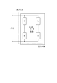
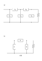
- FIG. 1 is a diagram illustrating a concept of a transformer 200 using a two-terminal pair circuit (four-terminal circuit).
- Z in k ⁇ R (k is a constant)
- the relationship needs to hold.
- the input impedance Z in changes linearly with respect to the load variation, and the transformation ratio is constant.
- the input impedance Z in has no reactance component.
- the input impedance Z in needs to have a real component of k ⁇ R and an imaginary component of 0.
- LILT Liad-Invariant Linear Transformer
- the transformer device 200 As described above, an output voltage proportional to the input voltage is obtained regardless of the resistance value R of the load. That is, the transformer 200 that converts the input voltage into the output voltage at a constant transformation ratio (1 / k) 1/2 is obtained.
- a transformer device 200 As a transformer, a conventional commercial frequency transformer or a high-frequency transformer becomes unnecessary. Therefore, a dramatic reduction in size and weight of the transformer and a cost reduction associated therewith can be realized. Furthermore, the problems of parasitic capacitance and leakage magnetic field generation, which are problems with high-frequency transformers, are eliminated, and a low-loss transformer can be realized.
- FIG. 2 is a diagram illustrating an example of the concept of the number n of elements constituting the circuit.
- the left figure apparently has three elements X 1 , X 2 , and X 3 .
- topologically equivalent X 1 and X 2 are counted as one, and X 3 that does not make sense as an electric circuit is not counted. Therefore, the left circuit configuration is the same as the right circuit configuration, and the number of elements n is one.
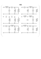
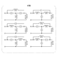
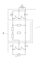
- FIG. 3 is a diagram showing four patterns of a circuit configuration that can be configured with a minimum number of elements of 4, and in the order of (a), (b), (c), and (d), “4A type”, “ They shall be referred to as “4B type”, “4C type”, and “4D type”.
- FIG. 4 is a diagram showing a 4A type circuit configuration.
- reactances of four reactance elements are X 1 , X 2 , X 3 , and X 4 , respectively, X 1 , X 2 in between the two wires, wherein the X 3, the X 4 in between two lines two-port network in 1 line is constructed.
- the input impedance Z in in this case is expressed by the upper part of the following equation.
- the input impedance Z in is represented by the lower stage. Note that “j” in each of the following expressions represents an imaginary number ( ⁇ 1) 1/2 .
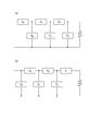
- FIG. 5 is a diagram showing Example 6 patterns of a 4A type circuit configuration.
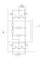
- FIG. 6 is a diagram showing a 4B type circuit configuration.
- X 1 in between two lines of two-port network
- X 2 on the first line X 3 between the two lines, and X 4 on the first line
- the input impedance Z in in this case is expressed by the upper part of the following equation.
- the input impedance Z in is represented by the lower stage.
- FIG. 7 is a diagram illustrating patterns of Example 6 of a 4B type circuit configuration.
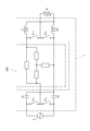
- FIG. 8 is a diagram showing a 4C type circuit configuration.
- reactances of four reactance elements are X 1 , X 2 , X 3 , and X 4 , respectively, X 1
- a two-terminal pair circuit is configured by a T-type circuit configured by X 2 between two lines, X 3 on the one line, and X 4 in parallel with a series body of X 1 and X 3. ing.
- the input impedance Z in in this case is expressed by the upper part of the following equation. Further, when the condition for setting the imaginary component to 0 by parallel resonance and series resonance is set, the input impedance Z in is represented by the lower stage.
- FIG. 9 is a diagram illustrating patterns of Example 6 of a 4C type circuit configuration.
- FIG. 10 is a diagram illustrating a 4D type circuit configuration.
- the input impedance Z in in this case is expressed by the upper part of the following equation. Further, when the condition for setting the imaginary component to 0 by parallel resonance and series resonance is set, the input impedance Z in is represented by the lower stage.
- FIG. 11 is a diagram illustrating Example 2 patterns of a 4D circuit configuration.
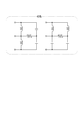
- the reactances of the five reactance elements are X A , X B , X C , X D , and X E , X A on the one line of the two-terminal pair circuit in order from the input side.
- X B between the two lines, X C on the one line, X D between the two lines, and X E on the one line constitute a two-terminal pair circuit.
- FIG. 12B shows a T-type circuit.
- the input impedance Z in is expressed by the upper part of the following equation, and the parameter condition of the lower part is necessary to make the imaginary component zero.
- R comes to the denominator, so it does not become LILT.
- Z in k ⁇ R
- an output voltage proportional to the input voltage can be obtained. Therefore, assuming that the reactances of the five reactance elements in the circuit of FIG. 12A are X A , X B , X C , X D , and X E , respectively, in the order of the two-terminal pair circuit as viewed from the input side. It is assumed that the two-terminal pair circuit is configured by X A on the line, X B between the two lines, X C on the one line, X D between the two lines, and X E on the one line.
- the input voltage needs to be alternating current.
- the reactances of the five reactance elements are X A , X B , X C , X D , and X E , respectively, the X between the two lines of the two-terminal pair circuit is sequentially viewed from the input side.
- a two-terminal pair circuit is configured by A 1, X B on one line, X C between two lines, X D on the one line, and X E between two lines.
- FIG. 13B shows a ⁇ -type circuit.
- the input impedance Z in is expressed by the upper part of the following equation, and the parameter condition of the lower part is necessary to make the imaginary component zero.
- R comes to the denominator, so it does not become LILT.
- Z in k ⁇ R
- an output voltage proportional to the input voltage can be obtained. Therefore, assuming that the reactances of the five reactance elements in the circuit of FIG. 13A are X A , X B , X C , X D , and X E , 2 in the two-terminal pair circuit in order from the input side.
- the two-terminal pair circuit is configured by X A between the lines, X B on the one line, X C between the two lines, X D on the one line, and X E between the two lines.
- the input voltage needs to be alternating current.
- the reactances of the six reactance elements are X A , X B , X C , X D , X E , and X F , respectively, on the one line of the two-terminal pair circuit in order from the input side X A , X B between the two lines, X C on the one line, X D between the two lines, X E on the one line, X F between the two lines, and so on. It is configured.
- R is not the LILT because R comes to the denominator.
- Z in k ⁇ R
- an output voltage proportional to the input voltage can be obtained. Therefore, when the reactances of the six reactance elements in the circuit of FIG. 14A are respectively X A , X B , X C , X D , X E , and X F , the two terminal pairs are sequentially viewed from the input side.
- the reactances of the six reactance elements are X A , X B , X C , X D , X E , and X F , respectively, the two terminals of the two-terminal pair circuit are connected in order from the input side.
- the above-described transformer device 200 using a lumped constant circuit can be used in combination with a transformer device having another configuration.
- a transformer device having another configuration.
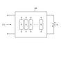
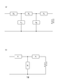
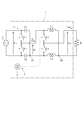
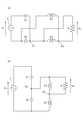
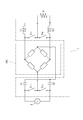
- FIG. 15 is a circuit diagram showing an example of the transformer device 1.
- the transformer device 1 is provided between an AC power supply 2 and a load R.
- the transformer 1 includes a pair of capacitors C1 and C2, a pair of inductors L1 and L2, four switches S r1 , S r2 , S b1 , and S b2 , and these switches S r1 , S r2 , S b1 , S and a switching control unit 3 for controlling on / off of b2 .
- the switching frequency of the switching control unit 3 is, for example, about 1 MHz.
- the switching frequency is preferably 1 MHz or more, but can be less than 1 MHz.
- the switches S r1 , S r2 , S b1 , S b2 and the switching control unit 3 constitute a switch device 4 that switches the circuit connection state of the transformer 1.
- the switches S r1 and S r2 operate in synchronization with each other, and the switches S b1 and S b2 operate in synchronization with each other.
- the pair of switches S r1 and S r2 and the pair of switches S b1 and S b2 operate so as to be alternately turned on.
- the switches S r1 , S r2 , S b1 , S b2 are, for example, semiconductor switching elements made of SiC elements or GaN elements. An SiC element or a GaN element can be switched at a higher speed than, for example, an Si element. Further, a sufficient breakdown voltage (for example, 6 kV / 1 unit is possible) can be obtained without connecting the elements in multiple stages.
- the pair of capacitors C1 and C2 are connected in series with each other at the connection point P1.
- AC power supply 2 is connected to both ends of the series body.
- the input voltage V in is applied to the series body of the pair of capacitors C1 and C2, and the input current I in flows.
- the pair of inductors L1 and L2 are connected in series with each other at the connection point P2. Then, the both ends of the series connection body, are applied input voltage V m over the capacitors C1, C2 flows input current I m.
- a current flows through the load R when one of the switches S r2 and S b2 is on.
- a voltage applied to the load R is V out
- an output current flowing from the transformer 1 to the load R is I out .
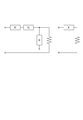
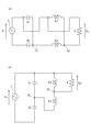
- FIG. 16B is a circuit diagram in which the same circuit diagram as in FIG. On the other hand, (a) in FIG.
- FIG. 17B is a circuit diagram in which the same circuit diagram as in FIG.
- the voltage taken out via the connection point P1 of the series body of the capacitors C1 and C2 is further taken out via the connection point P2 of the series body of the inductors L1 and L2.
- the input voltage may be output at about 1/4. This has been confirmed by the inventors' experiments.
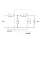
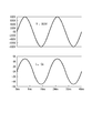
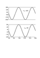
- FIG. 18 is a waveform diagram in which the upper part represents the input voltage to the transformer 1 and the lower part represents the input current.
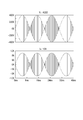
- FIG. 19 is a waveform diagram showing the voltage V m and the current I m at the intermediate stage of voltage transformation. This is actually constituted by a pulse train by switching, and has a waveform as shown in the figure as a whole.
- FIG. 20 is a waveform diagram in which the upper part represents the output voltage from the transformer 1 and the lower part represents the output current. As is clear from the comparison between FIGS. 18 and 20, the voltage is transformed to 1 ⁇ 4, and the current is quadrupled accordingly.
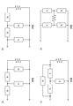
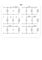
- FIG. 21 is a circuit diagram in which the transformer device 1 shown in FIG. 15 and the transformer device 200 having the 4A type circuit configuration are combined.
- a transformer device 200 is interposed between the capacitor stage and the inductor stage in the transformer device 1 shown in FIG.
- the transformer device 200 of the lumped constant circuit can be utilized using an environment where switching is performed at a high frequency of 1 MHz, for example. Even if the AC power supply 2 is replaced with a DC power supply, the transformer device 200 can be used because a switching waveform is input by switching the previous stage of the transformer device 1 (the same applies hereinafter).
- FIG. 22 is a circuit diagram in which the transformer 1 shown in FIG. 15 and the transformer 200 having the 4B type circuit configuration are combined.
- a transformer device 200 is interposed between the capacitor stage and the inductor stage in the transformer device 1 shown in FIG. In this way, by combining the transformation functions of the two types of transformers 1,200, a wide range of transformation ratios can be designed.
- FIG. 23 is a circuit diagram in which the transformer device 1 shown in FIG. 15 and the transformer device 200 having the 4C type circuit configuration are combined.
- a transformer device 200 is interposed between the capacitor stage and the inductor stage in the transformer device 1 shown in FIG. In this way, by combining the transformation functions of the two types of transformers 1,200, a wide range of transformation ratios can be designed.
- FIG. 24 is a circuit diagram in which the transformer device 1 shown in FIG. 15 and the transformer device 200 having the 4D circuit configuration are combined.
- a transformer device 200 is interposed between the capacitor stage and the inductor stage in the transformer device 1 shown in FIG. In this way, by combining the transformation functions of the two types of transformers 1,200, a wide range of transformation ratios can be designed.
- the capacitance of the cable and the inductance of the cable as the reactance element.
- the cable has an advantage that the pressure resistance performance can be easily secured and the cost is low.
Landscapes
- Engineering & Computer Science (AREA)
- Power Engineering (AREA)
- Ac-Ac Conversion (AREA)
- Coils Or Transformers For Communication (AREA)
Abstract
Description
一方、高周波トランスは、寄生容量の影響が回避できず、設計上の困難性がある。
なお、リアクタンス素子とは、誘導性リアクタンスを有するインダクタ、又は、容量性リアクタンスを有するキャパシタである。
本発明の実施形態の要旨としては、少なくとも以下のものが含まれる。
上記のような変圧装置では、負荷の抵抗値Rに関わらず、入力電圧に比例した出力電圧が得られる。すなわち、一定の変圧比(1/k)1/2で入力電圧を出力電圧に変換する変圧装置が得られる。このような変圧装置を変圧器として用いることにより、従来の商用周波トランスや、高周波トランスは不要となる。従って、変圧器の飛躍的な小型軽量化及び、それに伴う低コスト化を実現することができる。さらに、高周波トランスで課題となる寄生容量、漏れ磁界発生の問題も解消され、低損失な変圧器を実現できる。
(1/X1)+(1/X2)+(1/X3)=0 ∧ X2+X3+X4=0
この場合、入力インピーダンスZinは、Zin=(X2 2/X4 2)・Rとなり、負荷の抵抗値Rに比例し、入力電圧に比例した出力電圧が得られる。
なお、記号「∧」は論理積を表している(以下同様)。
X1+X2+X3=0 ∧ (1/X2)+(1/X3)+(1/X4)=0
この場合、入力インピーダンスZinは、Zin=(X1 2/X3 2)・Rとなり、負荷の抵抗値Rに比例し、入力電圧に比例した出力電圧が得られる。
X1+X3+X4=0 ∧ (1/X1)+(1/X2)+(1/X3)=0
この場合、入力インピーダンスZinは、Zin=(X1 2/X3 2)・Rとなり、負荷の抵抗値Rに比例し、入力電圧に比例した出力電圧が得られる。
X1+X2+X3+X4=0 ∧ (1/X1)+(1/X2)+(1/X3)+(1/X4)=0
この場合、入力インピーダンスZinは、Zin={(X1+X2)2/(X1-X2)2}・Rとなり、負荷の抵抗値Rに比例し、入力電圧に比例した出力電圧が得られる。
XA=-XB ∧ XE=-XD ∧ XC=XA+XE
の関係にあることが好ましい。
この場合、入力インピーダンスZinは、Zin=(XA 2/XE 2)・Rとなり、負荷の抵抗値Rに比例し、入力電圧に比例した出力電圧が得られる。
XA=-XB ∧ XE=-XD ∧ XC=XA・XE/(XA+XE)
の関係にあることが好ましい。
この場合、入力インピーダンスZinは、Zin=(XA 2/XE 2)・Rとなり、負荷の抵抗値Rに比例し、入力電圧に比例した出力電圧が得られる。
XA=XC=-XB ∧ XD=XF=-XE
の関係にあることが好ましい。
この場合、入力インピーダンスZinは、Zin=(XA 2/XF 2)・Rとなり、負負荷の抵抗値Rに比例し、入力電圧に比例した出力電圧が得られる。
XA=XC=-XB ∧ XD=XF=-XE
の関係にあることが好ましい。
この場合、入力インピーダンスZinは、Zin=(XA 2/XF 2)・Rとなり、負荷の抵抗値Rに比例し、入力電圧に比例した出力電圧が得られる。
この場合、スイッチングを行っている環境を利用して集中定数回路の変圧装置を活用することができる。
この場合、ケーブルは耐圧性能を容易に確保することができ、また、低コストである。
この場合、高周波でスイッチングを行っている環境を利用して集中定数回路の変圧装置を活用することができる。
<集中定数回路による変圧装置>
次に、本発明の実施形態に係る、集中定数回路を用いた変圧装置の詳細について説明する。
図1は、二端子対回路(四端子回路)による変圧装置200の概念を示す図である。変圧装置として機能するには、入力インピーダンスZinと負荷R(抵抗値R)との間に、
Zin=k・R (kは定数)
の関係が成り立つ必要がある。これにより、負荷変動に対して入力インピーダンスZinが線形に変化し、変圧比は一定である。また、入力インピーダンスZinは、リアクタンス成分を持たない。すなわち、入力インピーダンスZinは、実数成分がk・Rであり、虚数成分が0であることが必要である。このような入力インピーダンスZinとなる変圧装置200を、LILT(Load-Invariant Linear Transformer)と称する。
図4は、4A型の回路構成を示す図である。文言上で表現すると、例えば、4個のリアクタンス素子のリアクタンスをそれぞれX1,X2,X3,X4とすると、入力側から見て順に、二端子対回路の1線上にあるX1,2線間にあるX2,前記1線上にあるX3、2線間にあるX4によって二端子対回路が構成されている。この場合の入力インピーダンスZinは、以下の式の上段部で表される。また、並列共振及び直列共振により虚数成分を0にする条件を設定すると、入力インピーダンスZinは、下段部で表される。
なお、以下の各式中の「j」は虚数(-1)1/2を表す。

(1/X1)+(1/X2)+(1/X3)=0 ∧ X2+X3+X4=0
であるとき、言い換えれば、(1/X1)+(1/X2)+(1/X3)=0であり、かつ、X2+X3+X4=0であるとき、Zin=(X2 2/X4 2)・Rとなり、入力電圧に比例した出力電圧が得られる。なお、この機能発揮のためには、入力電圧は交流であることが必要である。
図5は、4A型の回路構成の実例6パターンを示す図である。
図6は、4B型の回路構成を示す図である。文言上で表現すると、例えば、4個のリアクタンス素子のリアクタンスをそれぞれX1,X2,X3,X4とすると、入力側から見て順に、二端子対回路の2線間にあるX1,1線上にあるX2,2線間にあるX3、前記1線上にあるX4によって二端子対回路が構成されている。この場合の入力インピーダンスZinは、以下の式の上段部で表される。また、並列共振及び直列共振により虚数成分を0にする条件を設定すると、入力インピーダンスZinは、下段部で表される。

X1+X2+X3=0 ∧ (1/X2)+(1/X3)+(1/X4)=0
であるとき、Zin=(X1 2/X3 2)・Rとなり、入力電圧に比例した出力電圧が得られる。なお、この機能発揮のためには、入力電圧は交流であることが必要である。
図7は、4B型の回路構成の実例6パターンを示す図である。
図8は、4C型の回路構成を示す図である。文言上で表現すると、例えば、4個のリアクタンス素子のリアクタンスをそれぞれX1,X2,X3,X4とすると、入力側から見て順に、二端子対回路の1線上にあるX1,2線間にあるX2,前記1線上にあるX3、によって構成されるT型回路と、X1及びX3の直列体に対して並列にあるX4とによって二端子対回路が構成されている。この場合の入力インピーダンスZinは、以下の式の上段部で表される。また、並列共振及び直列共振により虚数成分を0にする条件を設定すると、入力インピーダンスZinは、下段部で表される。

X1+X3+X4=0 ∧ (1/X1)+(1/X2)+(1/X3)=0
であるとき、Zin=(X1 2/X3 2)・Rとなり、入力電圧に比例した出力電圧が得られる。なお、この機能発揮のためには、入力電圧は交流であることが必要である。
図9は、4C型の回路構成の実例6パターンを示す図である。
図10は、4D型の回路構成を示す図である。文言上で表現すると、例えば、4個のリアクタンス素子のリアクタンスをそれぞれX1,X2,X3,X4とすると、入力側から見て順に、二端子対回路の2線間にあるX1,X2の第1直列体、及び、2線間にあるX3,X4の第2直列体を含み、第1直列体の相互接続点及び第2直列体の相互接続点が出力端子となる二端子対回路が構成されている。この場合の入力インピーダンスZinは、以下の式の上段部で表される。また、並列共振及び直列共振により虚数成分を0にする条件を設定すると、入力インピーダンスZinは、下段部で表される。

X1+X2+X3+X4=0 ∧ (1/X1)+(1/X2)+(1/X3)+(1/X4)=0
であるとき、Zin={(X1+X2)2/(X1-X2)2}・Rとなり、入力電圧に比例した出力電圧が得られる。なお、この機能発揮のためには、入力電圧は交流であることが必要である。
図11は、4D型の回路構成の実例2パターンを示す図である。
次に、要素数n=5の回路構成について考える。n=4よりも要素数は1つ増えるが、実用性はある。
図12の(a)は、n=5の第1例の回路構成を示す図である。文言上で表現すると、5個のリアクタンス素子のリアクタンスをそれぞれXA,XB,XC,XD,XEとすると、入力側から見て順に、二端子対回路の1線上にあるXA,2線間にあるXB,前記1線上にあるXC、2線間にあるXD、前記1線上にあるXE、によって二端子対回路が構成されている。

XA=-XB ∧ XE=-XD ∧ XC=XA+XE
の関係とする。この場合、入力インピーダンスZinは、Zin=(XA 2/XE 2)・Rとなり、負荷の抵抗値Rに比例し、入力電圧に比例した出力電圧が得られる。なお、この機能発揮のためには、入力電圧は交流であることが必要である。
図13の(a)は、n=5の第2例の回路構成を示す図である。文言上で表現すると、5個のリアクタンス素子のリアクタンスをそれぞれXA,XB,XC,XD,XEとすると、入力側から見て順に、二端子対回路の2線間にあるXA,1線上にあるXB,2線間にあるXC、前記1線上にあるXD、2線間にあるXE、によって二端子対回路が構成されている。

XA=-XB ∧ XE=-XD ∧ XC=XA・XE/(XA+XE)
の関係とする。
この場合、入力インピーダンスZinは、Zin=(XA 2/XE 2)・Rとなり、負荷の抵抗値Rに比例し、入力電圧に比例した出力電圧が得られる。なお、この機能発揮のためには、入力電圧は交流であることが必要である。
次に、要素数n=6の回路構成について考える。n=4よりも要素数は2つ増えるが、実用性はある。
図14の(a)は、n=6の第1例の回路構成を示す図である。文言上で表現すると、6個のリアクタンス素子のリアクタンスをそれぞれXA,XB,XC,XD,XE,XFとすると、入力側から見て順に、二端子対回路の1線上にあるXA,2線間にあるXB,前記1線上にあるXC、2線間にあるXD、前記1線上にあるXE、2線間にあるXF、によって二端子対回路が構成されている。
XA=XC=-XB ∧ XD=XF=-XE
の関係とする。
この場合、入力インピーダンスZinは、Zin=(XA 2/XF 2)・Rとなり、負負荷の抵抗値Rに比例し、入力電圧に比例した出力電圧が得られる。なお、この機能発揮のためには、入力電圧は交流であることが必要である。
図14の(b)は、n=6の第2例の回路構成を示す図である。文言上で表現すると、6個のリアクタンス素子のリアクタンスをそれぞれXA,XB,XC,XD,XE,XFとすると、入力側から見て順に、二端子対回路の2線間にあるXA,1線上にあるXB,2線間にあるXC、前記1線上にあるXD、2線間にあるXE、前記1線上にあるXF、によって二端子対回路が構成されている。
XA=XC=-XB ∧ XD=XF=-XE
の関係とする。
この場合、入力インピーダンスZinは、Zin=(XA 2/XF 2)・Rとなり、負荷の抵抗値Rに比例し、入力電圧に比例した出力電圧が得られる。なお、この機能発揮のためには、入力電圧は交流であることが必要である。
図15は、かかる変圧装置1の一例を示す回路図である。図において、変圧装置1は、交流電源2と、負荷Rとの間に設けられている。変圧装置1は、一対のキャパシタC1,C2と、一対のインダクタL1,L2と、4つのスイッチSr1,Sr2,Sb1,Sb2と、これらのスイッチSr1,Sr2,Sb1,Sb2のオン/オフを制御するスイッチング制御部3とを備えている。スイッチング制御部3のスイッチング周波数は、例えば1MHz程度である。なお、スイッチング周波数は1MHz以上が好ましいが、1MHz未満でも可能である。
また、一対のインダクタL1,L2は、接続点P2において互いに直列に接続されている。そして、その直列体の両端に、キャパシタC1,C2を介した入力電圧Vmが印加され、入力電流Imが流れる。負荷Rには、スイッチSr2,Sb2のいずれかがオンのとき電流が流れる。ここで、負荷Rに印加される電圧をVout、変圧装置1から負荷Rに流れる出力電流をIoutとする。
一方、図17の(a)は、図15における4つのスイッチSr1,Sr2,Sb1,Sb2のうち、下側にある2つのスイッチSb1,Sb2がオンで、上側にある2つのスイッチSr1,Sr2がオフであるときの、実体接続の状態を示す回路図である。また、図17の(b)は、(a)と同じ回路図を、階段状に書き換えた回路図である。
図19は、変圧の中間段階での電圧Vm、電流Imをそれぞれ表す波形図である。これは実際には、スイッチングによるパルス列によって構成され、全体として図示のような波形となる。
また、図20は、上が、変圧装置1からの出力電圧、下が、出力電流をそれぞれ表す波形図である。図18,図20の対比により明らかなように、電圧は1/4に変圧され、それに伴って、電流は4倍となる。
図21は、図15に示した変圧装置1と、上記4A型の回路構成を有する変圧装置200とを、組み合わせた回路図である。図において、図15に示した変圧装置1におけるキャパシタ段と、インダクタ段との間に、変圧装置200が介挿されている。このようにして、2種類の変圧装置1,200の変圧機能を組み合わせることにより、変圧比の広範囲な設計が可能となる。
また、この場合、例えば1MHzの高周波でスイッチングを行っている環境を利用して集中定数回路の変圧装置200を活用することができる。なお、交流電源2が仮に直流電源に置き換わったとしても、変圧装置200には、変圧装置1の前段のスイッチングによるスイッチング波形が入力されるので、使用可能である(以下同様)。
なお、上述のリアクタンス素子として、ケーブルのキャパシタンス及びケーブルのインダクタンスを利用することも可能である。
この場合、ケーブルは耐圧性能を容易に確保することができ、また、低コストであるという利点がある。
2 交流電源
3 スイッチング制御部
4 スイッチ装置
200 変圧装置
C1,C2 キャパシタ
L1,L2 インダクタ
Sb1,Sb2 スイッチ
Sr1,Sr2 スイッチ
P1,P2 接続点
R 負荷
Claims (12)
- 電源と抵抗値Rの負荷との間に設けられる変圧装置であって、
4以上の自然数をnとして、n個のリアクタンス素子を相互に接続して構成された二端子対回路を備え、
前記負荷の任意の抵抗値Rに対して、前記二端子対回路の入力インピーダンスZinは、その実数成分が、kを定数として、k・Rで表され、かつ、虚数成分が0である、変圧装置。 - 4個のリアクタンス素子のリアクタンスをそれぞれX1,X2,X3,X4とすると、入力側から見て順に、前記二端子対回路の1線上にあるX1,2線間にあるX2,前記1線上にあるX3、2線間にあるX4によって前記二端子対回路が構成され、以下の条件が満たされる請求項1に記載の変圧装置。
(1/X1)+(1/X2)+(1/X3)=0 ∧ X2+X3+X4=0 - 4個のリアクタンス素子のリアクタンスをそれぞれX1,X2,X3,X4とすると、入力側から見て順に、前記二端子対回路の2線間にあるX1,1線上にあるX2,2線間にあるX3、前記1線上にあるX4によって前記二端子対回路が構成され、以下の条件が満たされる請求項1に記載の変圧装置。
X1+X2+X3=0 ∧ (1/X2)+(1/X3)+(1/X4)=0 - 4個のリアクタンス素子のリアクタンスをそれぞれX1,X2,X3,X4とすると、入力側から見て順に、前記二端子対回路の1線上にあるX1,2線間にあるX2,前記1線上にあるX3、によって構成されるT型回路と、X1及びX3の直列体に対して並列にあるX4とによって前記二端子対回路が構成され、以下の条件が満たされる請求項1に記載の変圧装置。
X1+X3+X4=0 ∧ (1/X1)+(1/X2)+(1/X3)=0 - 4個のリアクタンス素子のリアクタンスをそれぞれX1,X2,X3,X4とすると、入力側から見て順に、前記二端子対回路の2線間にあるX1,X2の第1直列体、及び、2線間にあるX3,X4の第2直列体を含み、前記第1直列体の相互接続点及び前記第2直列体の相互接続点が出力端子となる前記二端子対回路が構成され、以下の条件が満たされる請求項1に記載の変圧装置。
X1+X2+X3+X4=0 ∧ (1/X1)+(1/X2)+(1/X3)+(1/X4)=0 - 5個のリアクタンス素子のリアクタンスをそれぞれXA,XB,XC,XD,XEとすると、入力側から見て順に、前記二端子対回路の1線上にあるXA,2線間にあるXB,前記1線上にあるXC、2線間にあるXD、前記1線上にあるXE、によって前記二端子対回路が構成され、
XA=-XB ∧ XE=-XD ∧ XC=XA+XE
の関係にある請求項1に記載の変圧装置。 - 5個のリアクタンス素子のリアクタンスをそれぞれXA,XB,XC,XD,XEとすると、入力側から見て順に、前記二端子対回路の2線間にあるXA,1線上にあるXB,2線間にあるXC、前記1線上にあるXD、2線間にあるXE、によって前記二端子対回路が構成され、
XA=-XB ∧ XE=-XD ∧ XC=XA・XE/(XA+XE)
の関係にある請求項1に記載の変圧装置。 - 6個のリアクタンス素子のリアクタンスをそれぞれXA,XB,XC,XD,XE,XFとすると、入力側から見て順に、前記二端子対回路の1線上にあるXA,2線間にあるXB,前記1線上にあるXC、2線間にあるXD、前記1線上にあるXE、2線間にあるXF、によって前記二端子対回路が構成され、
XA=XC=-XB ∧ XD=XF=-XE
の関係にある請求項1に記載の変圧装置。 - 6個のリアクタンス素子のリアクタンスをそれぞれXA,XB,XC,XD,XE,XFとすると、入力側から見て順に、前記二端子対回路の2線間にあるXA,1線上にあるXB,2線間にあるXC、前記1線上にあるXD、2線間にあるXE、前記1線上にあるXF、によって前記二端子対回路が構成され、
XA=XC=-XB ∧ XD=XF=-XE
の関係にある請求項1に記載の変圧装置。 - スイッチングを行う回路と、当該回路内に介挿された請求項1~請求項9のいずれか1項に記載の変圧装置とを含む変圧装置。
- 前記リアクタンス素子として、ケーブルのキャパシタンス及びケーブルのインダクタンスを利用する請求項1~請求項9のいずれか1項に記載の変圧装置。
- 前記スイッチングの周波数は少なくとも1MHzである請求項10に記載の変圧装置。
Priority Applications (3)
| Application Number | Priority Date | Filing Date | Title |
|---|---|---|---|
| US14/912,568 US10320305B2 (en) | 2013-08-29 | 2014-08-08 | Transformer |
| EP14839733.4A EP3041123A4 (en) | 2013-08-29 | 2014-08-08 | Transformer |
| KR1020157036907A KR20160047433A (ko) | 2013-08-29 | 2014-08-08 | 변압 장치 |
Applications Claiming Priority (2)
| Application Number | Priority Date | Filing Date | Title |
|---|---|---|---|
| JP2013178494A JP5695712B2 (ja) | 2013-08-29 | 2013-08-29 | 変圧装置 |
| JP2013-178494 | 2013-08-29 |
Publications (1)
| Publication Number | Publication Date |
|---|---|
| WO2015029744A1 true WO2015029744A1 (ja) | 2015-03-05 |
Family
ID=52586314
Family Applications (1)
| Application Number | Title | Priority Date | Filing Date |
|---|---|---|---|
| PCT/JP2014/070967 WO2015029744A1 (ja) | 2013-08-29 | 2014-08-08 | 変圧装置 |
Country Status (7)
| Country | Link |
|---|---|
| US (1) | US10320305B2 (ja) |
| EP (1) | EP3041123A4 (ja) |
| JP (1) | JP5695712B2 (ja) |
| KR (1) | KR20160047433A (ja) |
| CN (2) | CN104426381A (ja) |
| TW (1) | TWI610530B (ja) |
| WO (1) | WO2015029744A1 (ja) |
Families Citing this family (6)
| Publication number | Priority date | Publication date | Assignee | Title |
|---|---|---|---|---|
| JP5695712B2 (ja) * | 2013-08-29 | 2015-04-08 | 住友電気工業株式会社 | 変圧装置 |
| JP5695782B1 (ja) * | 2013-09-12 | 2015-04-08 | 住友電気工業株式会社 | 変圧装置 |
| JP6359950B2 (ja) | 2014-11-05 | 2018-07-18 | 住友電気工業株式会社 | 変圧装置 |
| JP6297963B2 (ja) | 2014-11-05 | 2018-03-20 | 住友電気工業株式会社 | 変圧装置 |
| JP6905452B2 (ja) * | 2017-11-08 | 2021-07-21 | 住友電気工業株式会社 | 変圧装置 |
| CN113537528B (zh) * | 2021-07-28 | 2022-05-03 | 贵州电网有限责任公司 | 一种输变电设备状态监测数据的预处理方法及系统 |
Citations (4)
| Publication number | Priority date | Publication date | Assignee | Title |
|---|---|---|---|---|
| JPH08305450A (ja) * | 1995-04-28 | 1996-11-22 | Tsubakimoto Chain Co | 交流電源装置及びこれに用いるインピーダンス変換器 |
| JP2002049428A (ja) * | 2000-08-04 | 2002-02-15 | Kansai Tlo Kk | イミタンス変換器、電源装置および非接触給電装置 |
| JP2002095241A (ja) * | 2000-09-14 | 2002-03-29 | Toshihisa Shimizu | イミタンス変換回路及びこれを使用したコンバータ |
| JP2002272127A (ja) * | 2001-03-07 | 2002-09-20 | Tsubakimoto Chain Co | 給電装置 |
Family Cites Families (6)
| Publication number | Priority date | Publication date | Assignee | Title |
|---|---|---|---|---|
| FR1064891A (fr) * | 1952-10-18 | 1954-05-18 | Csf | Perfectionnements aux réseaux transformateurs d'impédances |
| FR2549314B1 (fr) * | 1983-07-12 | 1985-11-08 | Thomson Csf | Quadrupole d'adaptation, independante de la frequence de fonctionnement, d'une reactance, et amplificateur a ondes progressives utilisant un tel quadrupole |
| US4951009A (en) * | 1989-08-11 | 1990-08-21 | Applied Materials, Inc. | Tuning method and control system for automatic matching network |
| JPH10174436A (ja) * | 1996-12-09 | 1998-06-26 | Mitsui Chem Inc | 圧電素子駆動回路 |
| CN102404908B (zh) * | 2010-09-08 | 2014-10-15 | 惠州元晖光电股份有限公司 | 用于电子变压器驱动led器件的稳定网络 |
| JP5695712B2 (ja) * | 2013-08-29 | 2015-04-08 | 住友電気工業株式会社 | 変圧装置 |
-
2013
- 2013-08-29 JP JP2013178494A patent/JP5695712B2/ja active Active
-
2014
- 2014-08-08 WO PCT/JP2014/070967 patent/WO2015029744A1/ja active Application Filing
- 2014-08-08 KR KR1020157036907A patent/KR20160047433A/ko not_active Application Discontinuation
- 2014-08-08 EP EP14839733.4A patent/EP3041123A4/en not_active Withdrawn
- 2014-08-08 US US14/912,568 patent/US10320305B2/en active Active
- 2014-08-19 TW TW103128454A patent/TWI610530B/zh not_active IP Right Cessation
- 2014-08-28 CN CN201410433064.0A patent/CN104426381A/zh active Pending
- 2014-08-28 CN CN201420492609.0U patent/CN204408198U/zh not_active Expired - Fee Related
Patent Citations (4)
| Publication number | Priority date | Publication date | Assignee | Title |
|---|---|---|---|---|
| JPH08305450A (ja) * | 1995-04-28 | 1996-11-22 | Tsubakimoto Chain Co | 交流電源装置及びこれに用いるインピーダンス変換器 |
| JP2002049428A (ja) * | 2000-08-04 | 2002-02-15 | Kansai Tlo Kk | イミタンス変換器、電源装置および非接触給電装置 |
| JP2002095241A (ja) * | 2000-09-14 | 2002-03-29 | Toshihisa Shimizu | イミタンス変換回路及びこれを使用したコンバータ |
| JP2002272127A (ja) * | 2001-03-07 | 2002-09-20 | Tsubakimoto Chain Co | 給電装置 |
Non-Patent Citations (3)
| Title |
|---|
| FALCONES, S. ET AL., POWER AND ENERGY SOCIETY GENERAL MEETING, 2010 IEEE, July 2010 (2010-07-01), pages 1 - 8 |
| KYOHEI YAMADA ET AL.: "Load-Invariant Constant-Voltage-Ratio Transformer without Employing Mutual Inductance", 2013 NEN PROCEEDINGS OF THE SOCIETY CONFERENCE OF IEICE TSUSHIN (2) B-9-3, 3 September 2013 (2013-09-03), pages 202, XP008182819 * |
| See also references of EP3041123A4 * |
Also Published As
| Publication number | Publication date |
|---|---|
| KR20160047433A (ko) | 2016-05-02 |
| TWI610530B (zh) | 2018-01-01 |
| EP3041123A4 (en) | 2017-05-10 |
| US20160211760A1 (en) | 2016-07-21 |
| JP2015050776A (ja) | 2015-03-16 |
| CN104426381A (zh) | 2015-03-18 |
| JP5695712B2 (ja) | 2015-04-08 |
| EP3041123A1 (en) | 2016-07-06 |
| US10320305B2 (en) | 2019-06-11 |
| CN204408198U (zh) | 2015-06-17 |
| TW201524109A (zh) | 2015-06-16 |
Similar Documents
| Publication | Publication Date | Title |
|---|---|---|
| WO2015029744A1 (ja) | 変圧装置 | |
| JP5695782B1 (ja) | 変圧装置 | |
| US10003316B2 (en) | Device and method for filtering electromagnetic interference | |
| TWI625034B (zh) | Transformer | |
| JP2002049428A (ja) | イミタンス変換器、電源装置および非接触給電装置 | |
| JP4290669B2 (ja) | ノイズ抑制回路 | |
| JP6210464B2 (ja) | 電気回路 | |
| JP6144709B2 (ja) | 変圧装置 | |
| RU2558690C2 (ru) | Устройство отбора мощности от линии электропередачи | |
| JP6905452B2 (ja) | 変圧装置 | |
| CN107112908B (zh) | 变压器 | |
| CN108712088A (zh) | 一种抑制eft骚扰的开关电源电路 |
Legal Events
| Date | Code | Title | Description |
|---|---|---|---|
| 121 | Ep: the epo has been informed by wipo that ep was designated in this application |
Ref document number: 14839733 Country of ref document: EP Kind code of ref document: A1 |
|
| REEP | Request for entry into the european phase |
Ref document number: 2014839733 Country of ref document: EP |
|
| WWE | Wipo information: entry into national phase |
Ref document number: 2014839733 Country of ref document: EP |
|
| ENP | Entry into the national phase |
Ref document number: 20157036907 Country of ref document: KR Kind code of ref document: A |
|
| WWE | Wipo information: entry into national phase |
Ref document number: 14912568 Country of ref document: US |
|
| NENP | Non-entry into the national phase |
Ref country code: DE |