WO2015025637A1 - 光電変換装置およびその製造方法 - Google Patents
光電変換装置およびその製造方法 Download PDFInfo
- Publication number
- WO2015025637A1 WO2015025637A1 PCT/JP2014/068614 JP2014068614W WO2015025637A1 WO 2015025637 A1 WO2015025637 A1 WO 2015025637A1 JP 2014068614 W JP2014068614 W JP 2014068614W WO 2015025637 A1 WO2015025637 A1 WO 2015025637A1
- Authority
- WO
- WIPO (PCT)
- Prior art keywords
- metal film
- photoelectric conversion
- openings
- metal
- light
- Prior art date
- Legal status (The legal status is an assumption and is not a legal conclusion. Google has not performed a legal analysis and makes no representation as to the accuracy of the status listed.)
- Ceased
Links
Images







Classifications
-
- H—ELECTRICITY
- H10—SEMICONDUCTOR DEVICES; ELECTRIC SOLID-STATE DEVICES NOT OTHERWISE PROVIDED FOR
- H10F—INORGANIC SEMICONDUCTOR DEVICES SENSITIVE TO INFRARED RADIATION, LIGHT, ELECTROMAGNETIC RADIATION OF SHORTER WAVELENGTH OR CORPUSCULAR RADIATION
- H10F77/00—Constructional details of devices covered by this subclass
- H10F77/30—Coatings
- H10F77/306—Coatings for devices having potential barriers
- H10F77/331—Coatings for devices having potential barriers for filtering or shielding light, e.g. multicolour filters for photodetectors
-
- H—ELECTRICITY
- H10—SEMICONDUCTOR DEVICES; ELECTRIC SOLID-STATE DEVICES NOT OTHERWISE PROVIDED FOR
- H10F—INORGANIC SEMICONDUCTOR DEVICES SENSITIVE TO INFRARED RADIATION, LIGHT, ELECTROMAGNETIC RADIATION OF SHORTER WAVELENGTH OR CORPUSCULAR RADIATION
- H10F39/00—Integrated devices, or assemblies of multiple devices, comprising at least one element covered by group H10F30/00, e.g. radiation detectors comprising photodiode arrays
- H10F39/10—Integrated devices
- H10F39/12—Image sensors
- H10F39/18—Complementary metal-oxide-semiconductor [CMOS] image sensors; Photodiode array image sensors
- H10F39/182—Colour image sensors
-
- H—ELECTRICITY
- H10—SEMICONDUCTOR DEVICES; ELECTRIC SOLID-STATE DEVICES NOT OTHERWISE PROVIDED FOR
- H10F—INORGANIC SEMICONDUCTOR DEVICES SENSITIVE TO INFRARED RADIATION, LIGHT, ELECTROMAGNETIC RADIATION OF SHORTER WAVELENGTH OR CORPUSCULAR RADIATION
- H10F39/00—Integrated devices, or assemblies of multiple devices, comprising at least one element covered by group H10F30/00, e.g. radiation detectors comprising photodiode arrays
- H10F39/80—Constructional details of image sensors
- H10F39/805—Coatings
-
- H—ELECTRICITY
- H10—SEMICONDUCTOR DEVICES; ELECTRIC SOLID-STATE DEVICES NOT OTHERWISE PROVIDED FOR
- H10F—INORGANIC SEMICONDUCTOR DEVICES SENSITIVE TO INFRARED RADIATION, LIGHT, ELECTROMAGNETIC RADIATION OF SHORTER WAVELENGTH OR CORPUSCULAR RADIATION
- H10F39/00—Integrated devices, or assemblies of multiple devices, comprising at least one element covered by group H10F30/00, e.g. radiation detectors comprising photodiode arrays
- H10F39/80—Constructional details of image sensors
- H10F39/805—Coatings
- H10F39/8057—Optical shielding
-
- H—ELECTRICITY
- H10—SEMICONDUCTOR DEVICES; ELECTRIC SOLID-STATE DEVICES NOT OTHERWISE PROVIDED FOR
- H10F—INORGANIC SEMICONDUCTOR DEVICES SENSITIVE TO INFRARED RADIATION, LIGHT, ELECTROMAGNETIC RADIATION OF SHORTER WAVELENGTH OR CORPUSCULAR RADIATION
- H10F39/00—Integrated devices, or assemblies of multiple devices, comprising at least one element covered by group H10F30/00, e.g. radiation detectors comprising photodiode arrays
- H10F39/80—Constructional details of image sensors
- H10F39/806—Optical elements or arrangements associated with the image sensors
-
- H—ELECTRICITY
- H10—SEMICONDUCTOR DEVICES; ELECTRIC SOLID-STATE DEVICES NOT OTHERWISE PROVIDED FOR
- H10F—INORGANIC SEMICONDUCTOR DEVICES SENSITIVE TO INFRARED RADIATION, LIGHT, ELECTROMAGNETIC RADIATION OF SHORTER WAVELENGTH OR CORPUSCULAR RADIATION
- H10F39/00—Integrated devices, or assemblies of multiple devices, comprising at least one element covered by group H10F30/00, e.g. radiation detectors comprising photodiode arrays
- H10F39/80—Constructional details of image sensors
- H10F39/806—Optical elements or arrangements associated with the image sensors
- H10F39/8067—Reflectors
-
- H—ELECTRICITY
- H10—SEMICONDUCTOR DEVICES; ELECTRIC SOLID-STATE DEVICES NOT OTHERWISE PROVIDED FOR
- H10F—INORGANIC SEMICONDUCTOR DEVICES SENSITIVE TO INFRARED RADIATION, LIGHT, ELECTROMAGNETIC RADIATION OF SHORTER WAVELENGTH OR CORPUSCULAR RADIATION
- H10F77/00—Constructional details of devices covered by this subclass
- H10F77/30—Coatings
- H10F77/306—Coatings for devices having potential barriers
- H10F77/331—Coatings for devices having potential barriers for filtering or shielding light, e.g. multicolour filters for photodetectors
- H10F77/334—Coatings for devices having potential barriers for filtering or shielding light, e.g. multicolour filters for photodetectors for shielding light, e.g. light blocking layers or cold shields for infrared detectors
Definitions
- the present invention relates to a photoelectric conversion device such as a color sensor and a manufacturing method thereof.
- the human eye does not feel much color change even when the color temperature of the room lighting is different, and this characteristic is generally called chromatic adaptation. For example, when entering a yellowish (low color temperature) incandescent room from a bluish (high color temperature) fluorescent room, the white walls of the room initially appear yellowish. However, after a while, the wall that looked yellowish appears white.
- the ambient lighting changes from moment to moment depending on the viewing location, so the color temperature is automatically adjusted like a color sensor. Sensors that detect the inequality are becoming more important.
- This color sensor is configured by separately sensing the spectrum of R (red), G (green), and B (blue) in the visible light region from ambient light.
- the color sensor is referred to as an RGB sensor.
- RGB sensor a plurality of photoelectric conversion elements are used to sense ambient light, and a device that becomes the photoelectric conversion elements is generally constituted by a photodiode.
- the photodiode itself cannot identify the color and can only detect the intensity of light (light quantity). Therefore, when an image is converted into an electrical signal, a color filter is placed on each photodiode to identify the color, and each of the three primary colors of light R (red), G (green), and B is applied to each photodiode. A color signal is acquired from the photodiode by detecting the amount of (blue) light.
- the optical wavelength selective filter having this structure uses an abnormal transmission phenomenon of light due to surface plasmon resonance excited by incident light.
- Patent Document 1 Japanese Patent Laid-Open No. 11-72607
- Patent Document 1 Japanese Patent Laid-Open No. 11-72607
- FIG. 8 a thin metal film 501 having a thickness of about 50 to 200 nm is formed, and holes finer than the transmission wavelength are formed in the metal film 501.
- FIG. 9 shows a spectral waveform that is transmitted when light enters the filter layer 500.
- the film and the insulating film have a single structure (uniformity of physical properties such as material and refractive index, uniformity of hole pitch and shape).
- Au, Ag, Al or the like is used as the metal material.
- Non-Patent Document 1 (Focus 26 ⁇ 3rd> Development of a color filter using surface plasmon resonance, NIMS, Toyota Central R & D Laboratories) A pitch is required.
- the pitch between the holes 502, 502, 502... Needs to be about 260 nm, as shown in FIG. The thickness needs to be about 80 to 180 nm.
- a pitch between the holes 502, 502, 502... Of about 260 nm is necessary for blue light transmission as described above.
- an N-type impurity layer such as phosphorus is introduced onto the P-type silicon substrate by ion implantation or the like to form the photoelectric conversion element.
- an electrode is formed of an AlCu material through an insulating film such as SiO 2 , and then SiO 2 is formed again and planarized by CMP (Chemical Mechanical Polishing) or the like.
- an Al material is formed to a thickness of about 150 nm using a sputtering apparatus, and a resist or the like is further coated thereon. This resist is exposed with an exposure apparatus such as a scanner using a mask with a hole array pattern, developed, and then etched with an etching facility to complete patterning.
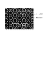
- the hole array is densely formed as shown in FIG. 10 to form the holes 502, the conditions must be carefully determined more than normal exposure. For example, when a large number of holes are adjacent to each other at a short distance such as a hole diameter of 100 nm or less and a pitch of 200 nm, a normal mask as shown in FIG. There was a problem that development was not possible. Therefore, a halftone mask or the like as shown in FIG. 14 is used. However, when the distance is closer, the mutual influence is still exerted. For this reason, the conditions are often determined in consideration of this mutual influence.
- FIG. 11 shows an example of the opening shape when exposure is performed under such non-uniform conditions.
- the hole diameter of the outer peripheral portion (and its surroundings) that is not surrounded by holes is processed to be small because there are no surrounding holes that are subject to interference.
- holes are processed by generating plasma in a reactive gas atmosphere by etching equipment and etching the metal film.
- the etching varies due to the density of the pattern. This phenomenon is called microloading effect.
- the etching rate is higher in the rough portion than in the dense portion.
- an increase in the contributed radical consumption and a decrease in the sidewall protective film formed of carbon, oxygen, and nitrogen released from the resist are considered.
- the etching rate is slower at the outermost peripheral portion that is not surrounded, and in some cases, only the outermost periphery (and the vicinity thereof) may be processed larger as shown in FIG.
- the resist After the etching, the resist is peeled off, and a SiO 2 film is deposited by a SiO 2 deposition apparatus to constitute a plasmonic filter.
- the transmission characteristics of the filter become non-uniform, and when spectral sensitivity is obtained using a photoelectric conversion element, as shown in FIG.
- the transmission characteristics are deteriorated when the non-uniform opening shown by the solid line is performed as compared with the case where the uniform opening shown by the broken line is processed.
- the half-value width of the transmitted spectral waveform increases, or transmission of a wavelength that should originally be suppressed occurs.
- the plasmonic filter selectively transmits the wavelength depending on the hole pitch and the hole diameter, there is a problem that if the hole diameter varies, the transmission characteristics are not uniform and desired characteristics cannot be obtained.
- an object of the present invention is to provide a photoelectric conversion device capable of preventing abnormal transmission of light having a wavelength that is not originally transmitted without variation in the hole diameter and reducing the half-value width of the spectral waveform, and its manufacture. It is to provide a method.
- the photoelectric conversion device of the present invention is A first photoelectric conversion element provided on a substrate; A first metal film formed on the first photoelectric conversion element via an insulating film and having a plurality of openings arranged periodically or aperiodically to form a plasmonic filter region; , And a second metal film covering a part of the plurality of openings of the first metal film.
- the manufacturing method of the photoelectric conversion device of the present invention includes: Forming a photoelectric conversion element on the substrate; On the substrate, a plurality of wiring layers are sequentially formed via an insulating layer, and the uppermost wiring layer of the plurality of wiring layers is formed so as to also serve as a second metal film, On the photoelectric conversion element, a first metal film having a plurality of openings arranged periodically or aperiodically to form a plasmonic filter region is formed on the plurality of openings of the first metal film. It is characterized by being formed through an insulating film so as to be partially covered with the second metal film.
- the second metal film covers a part of the plurality of openings of the first metal film constituting the plasmonic filter region, the influence of interference light from the adjacent opening at the time of exposure, Transmitted light from the opening whose shape is likely to be non-uniform due to the microloading effect during etching can be blocked, and thus desired wavelength selectivity can be ensured.
- FIG. 10 is a graph showing a spectral waveform transmitted through a filter layer described in Patent Document 1. It is a figure which shows an example of the hole array of a blue light transmissive filter. It is a SEM (scanning electron microscope) photograph after photo at the time of fine exposure. It is a SEM photograph after fine processing (etching). It is a figure explaining the interference of the transmitted light between the holes of a normal mask. It is a figure explaining the interference of the transmitted light between the holes of a halftone mask. It is a figure which shows the filter transmission characteristic by the difference in a processing state. It is a graph which shows the dielectric function of Al. It is a graph which shows the dielectric function of Au. It is a top view of the photoelectric conversion apparatus of 4th Embodiment of this invention. It is sectional drawing of the photoelectric conversion apparatus of 4th Embodiment of this invention.
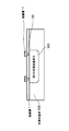
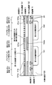
- FIG. 1 is a cross-sectional view of the photoelectric conversion device according to the first embodiment of the present invention.
- reference numeral 100 denotes a first conductive type (for example, P-type) semiconductor substrate as an example of a substrate
- 101 denotes a RGB corresponding to each of RGB, and each detects the amount of light of the three primary colors of RGB, for example, a photodiode.
- 1, 2, 3, 4 are insulating films made of, for example, SiO 2, 11 is a wiring layer, 20 is a via hole, 200 is a plasmonic filter region, 31 is a plasmonic filter region 200
- the first metal film, 32 is a second metal film, 41 is a plurality of openings formed in the first metal film 31, and 41a is an opening located on the outermost periphery among the plurality of openings 41.
- the opening 41a located on the outermost periphery is covered with the second metal film 32.
- the opening 41 a located on the outermost periphery among the plurality of openings 41 of the first metal film 31 constituting the plasmonic filter region 200 is formed by another second metal film 32. Since it is covered, it is possible to block the transmitted light from the opening 41a at the outermost periphery due to the influence of interference light from the adjacent opening at the time of exposure and the microloading effect at the time of etching, and the shape tends to be non-uniform, A plasmonic filter that secures a desired wavelength selectivity can be formed.
- the photoelectric conversion device of the first embodiment it is possible to prevent abnormal transmission of light having a wavelength that is not originally transmitted, and to reduce the half width of the spectral waveform.
- a second conductive type (N-type) impurity is introduced into a predetermined position on a first conductive type (P-type) semiconductor substrate 100 as an example of a substrate by ion implantation or the like, and heat treatment is performed.
- the photoelectric conversion element 101 such as a photodiode that converts incident light into an electric signal is formed.
- the semiconductor substrate 100 is covered with an insulating film 1 such as SiO 2, and a wiring layer 11 is formed on the insulating layer 1.
- the wiring layer 11 is connected to the cathode side and the anode side of the first photoelectric conversion element 101 via the via hole 20 in order to extract a photocurrent.
- an insulating layer 2 as an interlayer insulating film made of SiO 2 or the like is formed on the insulating film 1 and the wiring layer 11.
- a second metal film 32 is formed thereon using a metal such as Al or AlCu by sputtering.
- a portion of the second metal film 32 at a predetermined position is removed by photolithography using an exposure machine and etching using a dry etcher, and the remaining portion of the second metal film 32 and the insulating film 2 are removed.
- An insulating film 3 as an interlayer insulating film is formed so as to cover the second metal film 32 with SiO 2 or the like.
- a step is generated in the insulating film 3 between the portion where the second metal film 32 is present and the portion where the second metal film 32 is not present, but processing is performed until the insulating film 3 becomes completely flat by CMP. .
- a first metal film 31 is applied to the surface of the insulating film 3 that has been completely flattened by CMP, and specific light (for example, R (red), G (green)) is applied to the first metal film 31. , B (blue), etc.), the fine pattern of the wavelength selective filter is transmitted, so that the planarization of the surface is important.
- a first metal film 31 as a filter material is formed on the planarized insulating film 3 to a thickness of 150 nm by sputtering.
- the metal of the first metal film 31 of the filter material Al is most desirable from the unity of the material, but AlCu or AlSi which is more generally used for semiconductor manufacturing may be used.
- the film thickness of the first metal film 31 is desirably about 50 to 200 nm.
- the first metal film 31 since the same first metal film 31 also forms a light shielding metal portion (not shown), the first metal film 31 needs to have a film thickness that can block light wavelengths of 300 nm to 1200 nm.
- a photoresist 61 is applied on the first metal film 31, and a pattern of openings 61a, 61a,.
- the pattern of the openings 61a, 61a,... Is formed on the portion of the first metal film 31 on the light receiving opening on the photoelectric conversion element 101, and the outermost periphery opening 61a-1
- the metal film 32 is formed so as to be entirely covered.
- the first metal film 31 is etched using the photoresist 61 as a mask to form a first metal film 31 having a plurality of openings 41, 41,... As shown in FIG. Out of the plurality of openings 41, the outermost opening 41 a is covered with the second metal film 32.
- the outermost opening 41a As described above, by covering the outermost opening 41a with the second metal film 32 among the plurality of openings 41 of the first metal film 31, the influence of the interference light at the time of exposure and the microloading at the time of etching. Due to the effect, it is possible to block the light transmitted through the outermost peripheral opening 41a, which tends to have a non-uniform opening shape, and to suppress abnormal transmission such as increase of the half-value width of transmitted light and transmission of light of a wavelength that is not originally transmitted. it can.
- an insulating film 4 functioning as a protective film made of SiO 2 is formed on the first metal film 31 and the insulating film 3.
- the insulating film made of SiO 2 4 is formed by high density plasma CVD (chemical vapor deposition).
- the pattern of the plurality of openings 41, 41,... Of the first metal film 31 is periodically arranged in a two-dimensional manner.
- the opening 41 is formed by a through hole or a recess. These openings 41 are formed in a shape such as a circle, a quadrangle, or a triangle.
- the electrons vibrate similarly in the adjacent openings 41 and 41 and behave as collective excitation over the entire surface. Therefore, an arrangement in which the hole pitch between the adjacent openings 41 and the openings 41 takes the same distance is optimal. As shown in FIG. 10, if the six openings surround one opening, the hole pitch is constant and high color resolution can be obtained.
- the light having a wavelength of R (red: wavelength 660 nm), G (green: wavelength 540 nm), and B (blue: wavelength 440 nm) is formed by a plurality of openings 41, 41,... Periodically formed in the first metal film 31.
- R red: wavelength 660 nm
- G green: wavelength 540 nm
- B blue: wavelength 440 nm
- hole arrays arrays of openings 41
- Al, AlCu, or AlSi is used as the material of the first metal film 31 and the hole array is coated with the insulating film 4 made of SiO 2 , the conditions for exciting the surface plasmon by normal incidence of light are normalized.
- the frequency a / ⁇ 0.65.
- the period a of the hole array transmitting each light is calculated as 420 nm (R: red), 340 nm (G: green), and 260 nm (B: blue). From this equation, it is possible to select light to be transmitted by changing the period of the arrangement of the openings 41. Therefore, by forming a pattern having an array with a different period on one photomask, R, G, and B wavelength selective filters can be formed simultaneously.
- the opening 41a located in the outermost periphery among the several openings 41 of the 1st metal film 31 is covered with the 2nd metal film 32, depending on the case, it is several rows from the outermost periphery.
- the opening 41 up to the eyes may be covered with the second metal film 32, and only the opening 41a located at the corner among the openings 41a located at the outermost periphery may be covered with the second metal film 32.
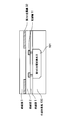
- FIG. 6 is a cross-sectional view of the photoelectric conversion device according to the second embodiment of the present invention.
- the same components as those of the photoelectric conversion device of the first embodiment shown in FIG. 1 are denoted by the same reference numerals as those of FIG. This will be described below.
- the photoelectric conversion device includes a second photoelectric conversion element 102 in addition to the first photoelectric conversion element 101, and the first metal film 131 includes the first and second photoelectric conversion elements 101. , 102, plasmonic filter regions 200, 200 having openings 41, and light shielding metal portions 131a, 131a, 131a for forming light shielding metal regions 301, 301, 301 are provided.
- the opening 41a located at the outermost periphery is covered with the second metal film 132.
- the opening 41 a located on the outermost periphery among the plurality of openings 41 of the first metal film 131 constituting the plasmonic filter region 200 is formed by another second metal film 132. Since it is covered, it is possible to block the transmitted light from the opening 41a at the outermost periphery due to the influence of interference light from the adjacent opening at the time of exposure and the microloading effect at the time of etching, and the shape tends to be non-uniform, A plasmonic filter that secures a desired wavelength selectivity can be formed.
- the photoelectric conversion device of the second embodiment it is possible to prevent abnormal transmission of light with a wavelength that is not originally transmitted, and to reduce the half-value width of the spectral waveform.
- the light shielding metal portion 131a of the first metal film 131 to be formed and the second metal film 132 opposite to the light shielding metal portion 131a cover regions outside the first and second photoelectric conversion elements 101 and 102. . Thereby, stray light can be prevented from entering the first and second photoelectric conversion elements 101 and 102, generation of false signals can be prevented, malfunction can be prevented, and durability can be improved.
- an N-type impurity is introduced into a predetermined position on a first conductivity type (P-type) semiconductor substrate 100 as an example of a substrate by a predetermined method such as ion implantation, and annealed at 1200 ° C.
- a predetermined method such as ion implantation, and annealed at 1200 ° C.
- two or more photoelectric conversion elements for example, a photodiode, a phototransistor, etc.
- a wiring layer 11 and a second metal film 132 are formed above the two first and second photoelectric conversion elements 101 and 102 on the semiconductor substrate 100 via insulating films 1 and 2.
- the second metal film 132 also functions as a wiring layer and constitutes a multilayer wiring together with the wiring layer 11.
- the second metal film 132 covers an opening 41a located on the outermost periphery among a plurality of openings 41 of the first metal film 131 described later, and the first photoelectric conversion element 101 and the second photoelectric conversion element. A region between the light-shielding metal 102 and the light-shielding metal portion 132a is also covered. If there is no light shielding metal portion 132a and only the second metal film 132 covers only the outermost peripheral opening 41a, the semiconductor substrate around the first and second photoelectric conversion elements 101 and 102 is moved to.
- the region between the first and second photoelectric conversion elements 101 and 102 is also covered with a light shielding metal portion 132a.
- the light leaking from the photoelectric conversion element such as oblique incidence is prevented from entering the adjacent photoelectric conversion element, and at the same time, the light leaking from the opening 41a having the nonuniform outermost hole diameter and shape is adjacent to the photoelectric conversion element. Can be prevented.
- the insulating film 3 is formed. After the insulating film 3 is formed, a step is generated between the portion where the second metal film 132 is present and the portion where the second metal film 132 is not present. Processing is performed by CMP until the insulating film 3 becomes completely flat. A first metal film 131 using Al or AlCu material is later formed on the surface of the insulating film 3, and specific light (for example, R (red), G, etc.) is formed on the first metal film 131. (Green), B (Blue), etc.) is transmitted, so that the fine pattern of the wavelength selective filter is photolithography, so that the planarization of the surface is important.
- specific light for example, R (red), G, etc.
- a first metal film 131 as a filter material is formed on the planarized insulating film 3 by sputtering to a thickness of 150 nm.
- the metal of this filter material is most preferably Al rather than the unity of the material, but AlCu or AlSi more commonly used in semiconductor manufacturing may be used, and if a wavelength selective film in the infrared region is desired to be formed, Au Or a metal such as Cu.
- the film thickness of the first metal film 131 is desirably about 50 to 200 nm. Further, since the light shielding metal portion 131a is also formed by the same first metal film 131, the first metal film 131 needs to have a film thickness capable of blocking a light wavelength of 300 nm to 1200 nm, for example.
- the first metal film 131 is not formed in a PAD (pad) portion that is an electrode extraction portion (not shown).
- a photoresist (not shown) is applied on the first metal film 131, and an opening pattern of a wavelength selection filter is formed on the photoresist by photolithography.
- the opening pattern of the wavelength selection filter is formed on the first metal film 131 on the light receiving opening on the first and second photoelectric conversion elements 101 and 102, and the outermost opening is the second opening. It is formed so as to be entirely covered with the metal film 132.
- the first metal film 31 is etched using a photoresist as a mask to form a first metal film 131 having a plurality of openings 41, 41,... As shown in FIG. Of the plurality of openings 41, the outermost opening 41 a is covered with the second metal film 132.
- the influence of interference light during exposure and microloading during etching are achieved. Due to the effect, it is possible to block the light transmitted through the outermost peripheral opening 41a, which tends to have a non-uniform opening shape, and to suppress abnormal transmission such as increase of the half-value width of transmitted light and transmission of light of a wavelength that is not originally transmitted. it can.
- the light shielding metal portion 131 a of the first metal film 131 and the light shielding metal portion 132 a of the second metal film 132 constituting the light shielding metal region 301 are formed between the first photoelectric conversion element 101 and the second photoelectric conversion element 102.
- the stray light is prevented from penetrating into the first and second photoelectric conversion elements 101 and 102 by being provided between and between the first and second photoelectric conversion elements 101 and 102.
- the openings 41 are formed by through holes or recesses, and the pattern of the plurality of openings 41 is two-dimensionally periodic.
- the periodic openings 41 are periodically arranged in a two-dimensional manner on the first metal film 131.
- the surface plasmon dispersion relation is incorporated into the aperture 41 thus formed, and the surface plasmon can be excited by light, and the first metal film 131 can function as a wavelength selection filter.
- electrons vibrate similarly in the adjacent openings 41 and behave as collective excitation over the entire surface. Therefore, an arrangement in which the hole pitches of the adjacent openings 41 and the openings 41 have the same distance is optimal. As described above, if the six openings surround one opening, the hole pitch is constant and high color resolution can be obtained.
- an insulating film 4 made of SiO 2 that functions as a protective film is formed.
- the front through-hole or recess of the opening 41 of the first metal film 131 formed in step it must also be formed to fill in SiO 2, made of SiO 2 by a high-density plasma CVD method insulating film 4 is coated on the first metal film 131.
- the second metal film 132 is an unevenly formed opening 41 a that is a part of the plurality of openings 41 of the first metal film 131 on the first photoelectric conversion element 101.
- the non-uniformly formed openings 41a that are a part of the plurality of openings 41 of the first metal film 131 on the second photoelectric conversion element 102, and the first light shielding metal portions 131a and 132a Since the region between the photoelectric conversion element 101 and the second photoelectric conversion element 102 is covered, the light and stray light transmitted through the non-uniformly formed openings 41a are the first and second photoelectric conversion elements 101 and 102. Can be prevented.
- the first metal film 131 is formed above the multilayer wiring
- the second metal film 132 is one wiring layer 132 of the plurality of wiring layers 11 and 132 of the multilayer wiring. Therefore, it is not necessary to newly form the second metal film 132 exclusively for exclusive use, and an increase in cost can be prevented.
- the second metal film 132 also serves as the uppermost wiring layer 132 of the plurality of wiring layers 11 and 132 of the multilayer wiring, the first metal film 131 and the second metal film 132 The distance is reduced, and light leaking to the first and second photoelectric conversion elements 101 and 102 can be reliably blocked.
- the distance between the first metal film 131 and the second metal film 132 for forming the plasmonic filter region is large, a part of the light is transmitted to the first and second photoelectric conversion elements 101 and 102. There is a risk of leakage and worsening the spectral sensitivity.
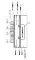
- FIG. 7 is a cross-sectional view of the photoelectric conversion device according to the third embodiment of the present invention.
- the same components as those of the photoelectric conversion device of the first embodiment shown in FIG. 1 are denoted by the same reference numerals as those of FIG. This will be described below.
- the photoelectric conversion device is a circuit built-in photoelectric conversion device, and a semiconductor substrate 100 as an example of a substrate is provided with a circuit unit 110 in addition to the first photoelectric conversion element 101. Further, the first metal film 231 of the photoelectric conversion device forms a plasmanic filter region 200 having a plurality of openings 41 on the first photoelectric conversion element 101, and further forms a light shielding metal region 302. It has light shielding metal portions 231a and 231a.
- the opening 41a located at the outermost periphery is covered with the second metal film 232 that also functions as the uppermost wiring layer. Yes.
- the opening 41 a located at the outermost periphery among the plurality of openings 41 of the first metal film 231 constituting the plasmonic filter region 200 is formed by the other second metal film 232. Since it is covered, it is possible to block the transmitted light from the opening 41a at the outermost periphery due to the influence of interference light from the adjacent opening at the time of exposure and the microloading effect at the time of etching, and the shape tends to be non-uniform, A plasmonic filter that secures a desired wavelength selectivity can be formed.
- the photoelectric conversion device of the third embodiment it is possible to prevent abnormal transmission of light with a wavelength that is not originally transmitted, and to reduce the half-value width of the spectral waveform.
- the light shielding metal portion 231a and the second metal film 232 of the first metal film 231 to be formed are regions outside the first photoelectric conversion element 101 and the circuit portion 110, and the first photoelectric conversion element 101 and the circuit portion. 110 is covered. Thereby, stray light can be prevented from entering the first photoelectric conversion element 101 and the circuit unit 110, generation of a false signal can be prevented, malfunction can be prevented, and durability can be improved.
- the first metal layer 231 and thus the light shielding metal portion 231a are grounded via a wiring (not shown) and are set to the ground potential.
- the first metal layer 231 and the light shielding metal portion 231a have a shielding effect against electrical noise as well as light shielding.
- the electrical noise can escape to the grounded potential, so the first metal layer 231 and the light shielding metal portion
- the electrical noise does not adversely affect the circuit unit 110 below 231a. That is, the light shielding metal portion 231a functions as a shield that prevents light from entering and protects the circuit portion 110 and the like from electrical noise.
- the light shielding metal portion 231a covers an area of 1/2 or more of the surface of the substrate 100.
- the area of the original first metal layer 231 to be etched can be reduced, and the occurrence of deposits or the like can be suppressed when the original first metal layer 231 is etched with a metal etcher or the like. it can.
- a first photoelectric conversion element 101 and a first photoelectric conversion element 101 are formed at predetermined positions of a semiconductor substrate 100 as an example of a substrate using a photolithography / ion implantation / etching facility.
- a circuit portion 110 for processing an electrical signal from the circuit is formed.
- This circuit portion may be a CMOS or a bipolar element.
- a region for forming a PAD (pad) unit 401 which is a terminal for outputting an electric signal is also secured in addition to the circuit unit 100.
- wiring layers 11, 12, and 232 constituting a multilayer wiring are disposed via insulating films 1 to 3.
- This wiring layer 232 is the second metal film 232 and covers the opening 41 a located on the outermost periphery among the plurality of openings 41 of the first metal film 231 constituting the plasmonic filter region 200.
- the second metal film 232 has a function as a wiring layer for normal multilayer wiring and a function of covering the opening 41 a located at the outermost periphery among the plurality of openings 41 of the first metal film 231. .
- an insulating film 4 is formed. After the formation of the insulating film 4, a step is generated between a portion where the second metal film 232 is present and a portion where the second metal film 232 is not present, but the second metal film 232 is formed without forming a shield metal portion in the second metal film 232. Since the insulating film 4 is formed on the insulating film 4, only a protruding step is generated in the insulating film 4.
- this protrusion-like step is subject to polishing pressure locally in the CMP process, so that it can be easily polished and can be easily flattened, and the polishing time can be suppressed. Thereby, the occurrence of dishing is suppressed, and the shape is easy to flatten.
- the slurry is preferably ceria in order to ensure flatness. Processing is performed by CMP using ceria until it is completely flat.
- the first metal film 231 is formed on the surface of the insulating film 4 later, and the wavelength selection filter of the first metal film 231 for transmitting specific light (for example, R, G, B, etc.).
- the planarization of this surface is important. This is because by increasing the numerical aperture (NA) of exposure for miniaturization, even if the depth of focus becomes shallow, the exposure can be accurately performed by flattening.
- NA numerical aperture
- a first metal film 231 is formed as a filter material on the surface of the planarized insulating film 4 to a thickness of 150 nm using a sputtering or vapor deposition apparatus.
- the metal of the filter material Al is most desirable than unity of the material, but AlCu or AlSi which is more generally used for semiconductor manufacturing may be used.
- the film thickness of the first metal film 231 is desirably about 50 to 200 nm. Further, in order to form the light shielding metal portion 231a on the same first metal film 231, the first metal film 231 needs to have a film thickness that can block light having a light wavelength of 300 nm to 1200 nm.
- a metal film is not formed on the PAD part 401 which is an electrode extraction part.
- a SiO 2 film (not shown) and an organic BARC (Bottom Anti Reflective Coating) are formed on the first metal film 231.
- This SiO 2 film is necessary for removing deposits formed on the filter surface by lift-off during etching performed later.
- BARC is used to suppress reflection on the surface of a metal such as Al and facilitate fine processing.
- anti-reflection layers like Ti / TiN are formed on the surface of AlCu in the multilayer wiring of the semiconductor process, but plasmon resonance is generated in Al, so it is used in this filter. Such a film is not formed and surface reflection is suppressed.
- a resist (not shown) is applied, and an opening pattern of the wavelength selection filter is formed by photolithography.
- openings of 130 nm are formed at a pitch of 260 nm.
- openings of 170 nm are formed at a pitch of 340 nm.
- openings of R (red) for example, openings of 210 nm are formed at a pitch of 420 nm.
- etching is performed in the order of BARC / SiO 2 / Al using a metal etcher, and the resist / BARC / SiO 2 is removed, thereby forming a pattern of the plurality of openings 41 that are the wavelength selection filters of the first metal film 231.
- the pattern of the plurality of openings 41 of the wavelength selection filter is formed on the first metal film 231 above the light receiving opening on the first photoelectric conversion element 101.
- the pattern of the openings 41 is periodically arranged in a two-dimensional manner and is formed by through holes or recesses.
- the surface plasmon dispersion relation is incorporated into the openings 41 periodically arranged in a shape, and the surface plasmons can be excited by light, and the first metal film 231 can function as a wavelength selection filter.
- the insulating film 5 functioning as a protective film made of SiO 2 is formed as shown in FIG.
- the opening (through hole or recess) 41 of the first metal film 231 formed in the previous step it must also be formed to fill in SiO 2, made of SiO 2 by a high-density plasma CVD method insulation A film 5 is formed.
- the second metal film 232 includes the non-uniformly formed openings 41 a that are a part of the plurality of openings 41 of the first metal film 231 on the first photoelectric conversion element 101.
- the light shielding metal portion 231a of the first metal film 231 covers the region between the first photoelectric conversion element 101 and the circuit portion 110, so that stray light is generated by the first photoelectric conversion element 101 and the circuit portion. 110 can be prevented from entering.
- the first metal film 231 is formed above the multilayer wiring
- the second metal film 232 is a wiring of one of the plurality of wiring layers 11, 12, 232 of the multilayer wiring. Since it also serves as the layer 232, it is not necessary to newly form the second metal film 232 separately for exclusive use, and an increase in cost can be prevented.
- the first metal film 231 can be additionally mounted without changing the process of the circuit built-in photoelectric conversion device including the circuit unit 110, and in addition, the second metal film 232 has a wiring layer of a multilayer wiring. Therefore, there is a merit that process integration is easy.
- the second metal film 232 also serves as the uppermost wiring layer 232 of the plurality of wiring layers 11, 12, and 232 of the multilayer wiring, and thus the first metal film 231 and the second metal film 232. , And the light leaking to the first photoelectric conversion element 101 and the circuit unit 110 can be reliably blocked.
- the spectral sensitivity may be deteriorated.
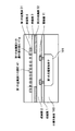
- (Fourth embodiment) 18 and 19 are a plan view and a cross-sectional view of a photoelectric conversion device according to a fourth embodiment of the present invention. 19, about the same component as the component of the photoelectric conversion apparatus of 3rd Embodiment shown in FIG. 7, the same reference number as the component of FIG. 7 is attached
- omitted about only a different component. This will be described below.
- a plurality of slits 841 as an example of a plurality of openings are provided in the first metal film 831 as shown in the plan view of FIG.
- the plurality of slits 841, 841, 841... are arranged in the horizontal direction at regular intervals.
- the second metal film 832 includes all the regions of the slits 841a, 841a at both ends of the plurality of slits 841, 841, 841... And the plurality of slits 841, 841 other than both ends. , 841... 841b, 841b, 841b, 841b,. That is, the second metal film 832 covers portions located on the outermost periphery of the plurality of slits 841, 841, 841.
- a plasmonic filter region 1200 positioned above the first photoelectric conversion element 101 is formed by a plurality of slits 841, and a light shielding metal region 1302 is formed by a light shielding metal portion 831 a.
- the first metal film 831 is grounded by a wiring (not shown), and the metal film 831 portion of the plasmonic filter region 1200 and the light shielding metal portion 831 are set to the ground potential.
- the portion corresponding to the plasmonic filter region 1200 of the metal film 831 and the light shielding metal portion 831 are electrically connected, but the plasmonic filter region 1200 of the metal film 831 is electrically connected.
- the corresponding part and the light shielding metal part 831 may be electrically separated. In this case, grounding the portion of the metal film 831 corresponding to the plasmonic filter region 1200 to the ground potential is important for improving the wavelength selection function of the plasmonic filter.
- the photoelectric conversion device of the fourth embodiment it is possible to prevent abnormal transmission of light with a wavelength that is not originally transmitted, and to reduce the half width of the spectral waveform.
- the second metal film Reference numeral 832 covers a region outside the first photoelectric conversion element 101. Thereby, stray light can be prevented from entering the first photoelectric conversion element 101, generation of a false signal can be prevented, malfunction can be prevented, and durability can be improved.
- the first metal film 831 is grounded and has a ground potential, the potential of the portion of the first metal film 831 constituting the plasmonic filter region 1200 is stabilized, and the behavior of electrons is improved. Stable and good wavelength selectivity. If the potential of the portion of the first metal film 831 in the plasmonic filter region 1200 fluctuates, the wavelength selectivity is adversely affected.
- the light shielding metal portion 831a of the first metal film 831 is grounded and has a ground potential, the light shielding metal portion 831a blocks light and transmits light to the first photoelectric conversion element 101. It functions not only as an optical shield that prevents intrusion but also as an electrical shield that protects the circuit portion 110 and the like from electrical noise.
- the light shielding metal portion 831 a covers an area of 1 ⁇ 2 or more of the surface of the substrate 100. Accordingly, the area of the original first metal layer 831 to be etched can be reduced, and generation of deposits or the like can be suppressed when the original first metal layer 831 is etched with a metal etcher or the like. it can.
- a first photoelectric conversion element 101 and a first photoelectric conversion element 101 are formed at predetermined positions of a semiconductor substrate 100 as an example of a substrate using a photolithography / ion implantation / etching facility.
- a circuit portion 110 for processing an electrical signal from the circuit is formed.
- the circuit unit 110 may be a CMOS or a bipolar element.
- a region for forming a PAD (pad) unit 401 which is a terminal for outputting an electric signal is also secured in addition to the circuit unit 100.
- wiring layers 11, 12, and 832 constituting a multilayer wiring are arranged via insulating films 1 to 3.
- the wiring layer 832 is the second metal film 832, and is formed at the outermost end in the horizontal direction among the plurality of slits 841 as the plurality of openings of the first metal film 831 constituting the plasmonic filter region 1200.
- the slit 841a is positioned, and both longitudinal ends 841b, 841b, 841b,... Of the plurality of slits 841, 841, 841,.
- the second metal film 832 functions as a wiring layer for normal multilayer wiring and the outermost periphery of the plurality of slits 841 of the first metal film 831 (outermost of the plurality of slits 841 in the lateral direction). It has a function of covering the slits 841a and 841a located at the ends and the longitudinal ends 841b and 841b) of the plurality of slits 841 other than the lateral ends.
- the insulating film 4 is formed. After the formation of the insulating film 4, a step is generated between the portion where the second metal film 832 is present and the portion where the second metal film 832 is not present. However, without forming the shield metal portion in the wiring layers 11, 12, 832, Since the insulating film 4 is formed on the metal film 832, only a protruding step is generated in the insulating film 4. Unlike the planar step, this protrusion-like step is subject to polishing pressure locally in the CMP process, so that it can be easily polished and can be easily flattened, and the polishing time can be suppressed.
- the slurry is preferably ceria in order to ensure flatness. Processing is performed by CMP using ceria until it is completely flat.
- the planarization of this surface is important. This is because by increasing the numerical aperture (NA) of exposure for miniaturization, even if the depth of focus becomes shallow, the exposure can be accurately performed by flattening.
- NA numerical aperture
- a first metal film 831 is formed as a filter material on the surface of the planarized insulating film 4 to a thickness of 150 nm using a sputtering or vapor deposition apparatus.
- the metal of the filter material Al is most desirable than unity of the material, but AlCu or AlSi which is more generally used for semiconductor manufacturing may be used.
- the film thickness of the first metal film 831 is preferably about 50 to 200 nm.
- the first metal film 831 needs to have a thickness capable of blocking light having a light wavelength of 300 to 1200 nm.
- a metal film is not formed on the PAD part 401 which is an electrode extraction part.
- a SiO 2 film (not shown) and an organic BARC (Bottom Anti Reflective Coating) are formed on the first metal film 831.
- This SiO 2 film is necessary for removing deposits formed on the filter surface by lift-off during etching performed later.
- BARC is used to suppress reflection on the surface of a metal such as Al and facilitate fine processing.
- anti-reflection layers like Ti / TiN are formed on the surface of AlCu in the multilayer wiring of the semiconductor process, but plasmon resonance is generated in Al, so it is used in this filter. Such a film is not formed and surface reflection is suppressed.
- a resist (not shown) is applied, and an opening pattern of the wavelength selection filter is formed with a slit structure by photolithography.
- B blue
- G green
- openings having a pitch of 340 nm and a width of 170 nm are formed with a slit structure.
- R red
- openings with a pitch of 420 nm and a width of 210 nm are formed with a slit structure.
- etching is performed in the order of BARC / SiO 2 / Al using a metal etcher, and the resist / BARC / SiO 2 is removed, so that a plurality of openings having a slit structure which is a wavelength selection filter of the first metal film 831 ( Slit) 841 pattern is formed.
- the pattern of the plurality of openings 841 of the wavelength selection filter is formed on the first metal film 831 on the light receiving opening on the first photoelectric conversion element 101.
- the arrangement pattern of the openings (slits) 841 is a slit structure in which the slits 841 are periodically arranged in the horizontal direction, and the slits 841 are formed by elongated through holes or recesses.
- a slit structure is formed on the first metal film 831 when light enters the first metal film 831 of the photoelectric conversion device with a built-in circuit.
- the surface plasmon dispersion relationship is incorporated into the openings 841 periodically arranged in the above, so that the surface plasmons can be excited by light, and the first metal film 831 can function as a wavelength selection filter.
- electrons vibrate similarly in the adjacent slits 841 and behave as collective excitation over the entire surface. Therefore, an arrangement in which the slit pitches of the adjacent slits 841 and 841 have the same distance is optimal. As shown in the plan view of FIG.
- the outermost peripheral slits with poor processing accuracy (the outermost slits 841a and 841a in the lateral direction of the plurality of slits 841 and the longitudinal ends 841b of the plurality of slits 841). , 841b) is shielded by the second metal film 832 and does not contribute as a plasmonic filter. Therefore, the slit pitch is constant and high color resolution can be obtained.
- the insulating film 5 functioning as a protective film made of SiO 2 is formed as shown in FIG.
- the opening (through hole or recess) 841 of the first metal film 831 formed in the previous step it must also be formed to fill in SiO 2, made of SiO 2 by a high-density plasma CVD method insulation A film 5 is formed.
- the first metal films 32, 132 are disposed between the first metal films 31, 131, 231, 831 constituting the plasmonic filter regions 200, 1200 and the substrate 100.
- 232, 831 are provided with second metal films 32, 132, 232, 832 covering the openings 41a, 841a located at the outermost periphery and the end portion 841b of the opening 841 among the plurality of openings 41, 841.
- a second metal film that covers the opening located on the outermost periphery may be provided on the upper side of the first metal film constituting the monic filter region. That is, a first metal film that forms a plasmonic filter region may be provided between the second metal film and the substrate.
- the photoelectric conversion device of the present invention is A first photoelectric conversion element 101 provided on the substrate 100; A plurality of openings 41, which are formed on the first photoelectric conversion element 101 via insulating films 1, 2, 3 and arranged periodically or aperiodically to form a plasmonic filter region. A first metal film 31, 131, 231, 831 having 841; And a second metal film 32, 132, 232, 832 covering a part of the plurality of openings 41, 841 of the first metal films 31, 131, 231, 831.
- the second metal films 32, 132, 232, and 832 partially open the openings 41 and 841 of the first metal films 31, 131, 231, and 831 that are expected to be formed unevenly.
- the first metal films 31, 131, 231, and 831 are covered by the second metal films 32, 132, 232, and 832 so that the light transmitted through the uneven portions of the openings 41 and 841 is blocked by the first metal films 32, 132, 232, and 832 It is possible to prevent it from reaching the photoelectric conversion element 101.
- a part of the plurality of openings 41 and 841 of the first metal films 31, 131, and 231 is arranged on the outermost periphery among the plurality of openings 41 and 841 of the first metal films 31, 131, and 231. Not only the openings 41a, 841a, and 841b that are positioned, but also the openings 41 and 841 that are located on the inner side of the outermost peripheral openings 41a and 841a, for example, from the outside, may be included.
- the second metal films 32, 132, 232, and 832 are a part 41 a of an opening located at least on the outermost periphery among the plurality of openings 41 and 841 of the first metal films 31, 131, 231, and 831. 841a and 841b are covered.
- the openings 41 a, 841 a and 841 b located at the outermost periphery are not surrounded by the openings 41 and 841. Therefore, it is more specific than the openings 41 and 841 in the central region surrounded by the openings 41 and 841, and is likely to be non-uniform due to exposure or etching.
- the light transmitted through the specific openings 41a, 841a, 841b can be blocked by the second metal films 32, 132, 232, 832, and therefore, the non-uniform openings 41a, 841a, 841b.
- the disturbed transmitted light does not contribute as a photocurrent, and an increase in the half width can be prevented.
- the outermost opening 41 a among the plurality of openings 41 of the first metal films 31, 131, and 231 has a unique size, but the corner opening 41 a is particularly unique. Because of the size, it is preferable to cover the opening 41a in the corner portion with the second metal films 32, 132, 232 among the outermost openings 41a.
- a second photoelectric conversion element 102 provided on the substrate 100 is provided,
- the first metal film 131 is formed on the first and second photoelectric conversion elements 101, 102 via insulating films 1, 2, 3,
- the second metal film 132 includes a part of the plurality of openings 41 of the first metal film 131 on the first photoelectric conversion element 101 and the first metal film 131 on the second photoelectric conversion element 102. And a region between the first photoelectric conversion element 101 and the second photoelectric conversion element 102 is covered.
- the second metal film 132 covers the non-uniformly formed openings 41a among the plurality of openings 41 of the first metal film 131, and the light transmitted through the openings 41a is second. Can be prevented from entering the first and second photoelectric conversion elements 101 and 102, and the second metal film 132 can be connected to the first photoelectric conversion element 101 and the first photoelectric conversion element 101. Since the region between the two photoelectric conversion elements 102 is covered, the second metal film 132 can also function as a light shielding metal that blocks stray light.
- a circuit unit 110 provided on the substrate 100, A multilayer wiring composed of a plurality of wiring layers 11, 12, 232, and 832 formed on the substrate 100 via insulating films 1, 2, 3, The first metal films 231 and 831 are formed above the multilayer wiring, The second metal films 232 and 832 also serve as one of the wiring layers 11, 12, 232, and 832 of the multilayer wiring.
- the second metal films 232 and 832 also serve as one wiring layer 232 and 832 of the plurality of wiring layers 11, 12, 232, and 832 of the multilayer wiring.
- the metal films 232 and 832 do not need to be newly formed exclusively for exclusive use, and an increase in cost can be prevented.
- the first metal film 231 can be additionally mounted without changing the process of the circuit built-in photoelectric conversion device itself including the circuit unit 110, and in addition, the second metal films 232 and 832 can be formed as multi-layer wirings. Since the layers 232 and 832 can also be used, there is an advantage that process integration is easy.
- the second metal films 132, 232, and 832 also serve as the uppermost wiring layers 132, 232, and 832 among the plurality of wiring layers 11, 12, 132, and 232 of the multilayer wiring.
- the second metal films 132, 232, and 832 are the uppermost wiring layers 132, 232, and 832 among the plurality of wiring layers 11, 12, 132, 232, and 832 of the multilayer wiring. Therefore, the distance between the first metal films 131, 231, 831 and the second metal films 132, 232, 832 is reduced, and the first and second photoelectric conversion elements 101, 102 and the circuit unit 110 are reduced. It is possible to reliably block light leaking into the water.
- the distance between the first metal films 131, 231 and 831 and the second metal films 132, 232 and 832 for constituting the plasmonic filter region is large, a part of the light is transmitted to the first and second light beams. This may leak into the photoelectric conversion elements 101 and 102 and the circuit unit 110 to deteriorate the spectral sensitivity or cause malfunction.
- the first and second metal films 31, 131, 231, 831, 32, 132, 232, and 832 are made of Al or AlCu.
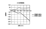
- the dielectric function of Al is shown in FIG.
- the physical property of the plasmon resonance is such that the real part of the dielectric function is small and the imaginary part is large.
- Al or AlCu metal that satisfies the above conditions in the wavelength range of 300 to 700 nm, such as Al, is desirable.
- the thickness of the second metal films 32, 132, 232, and 832 is at least a thickness that prevents transmission of light.
- the wavelength of light that prevents light from passing through the second metal films 32, 132, 232, and 832 is not less than 300 nm and not more than 1200 nm.
- the first metal films 31, 131, 231, and 831 transmit the three primary colors of light.
- the plurality of openings 841 of the first metal film 831 are slits 841.
- At least a portion constituting the plasmonic filter region 1200 is grounded.
- At least a portion of the first metal film 831 that constitutes the plasmonic filter region 1200 is grounded and has a ground potential, so that the plasmonic filter region 1200 is configured.
- the potential of the portion of the first metal film 831 to be stabilized is stabilized, the behavior of electrons is stabilized, and the wavelength selectivity is improved.
- the manufacturing method of the photoelectric conversion device of the present invention is as follows: Photoelectric conversion elements 101 and 102 are formed on a substrate 100; A plurality of wiring layers 11, 12, 132, 232, and 832 are sequentially formed on the substrate 100 via the insulating films 1, 2, and 3, and the plurality of wiring layers 11, 12, 132, 232, and 232 are formed. 832, the uppermost wiring layers 132, 232, and 832 are formed so as to also serve as the second metal films 132, 232, and 832, On the photoelectric conversion element 101, first metal films 131, 231, and 831 having a plurality of openings 41 and 841 arranged periodically or aperiodically to form a plasmonic filter region are formed on the photoelectric conversion element 101. A plurality of openings 41, 841 of one metal film 131, 231, 831 are formed through insulating films 1, 2, 3, 4 so as to be covered with the second metal films 132, 232, 832. It is characterized by doing.
- a photoelectric conversion device that can prevent abnormal transmission of light with a wavelength that does not originally pass through and can reduce the half-value width of the spectral waveform.
- Insulating film 11 12, 132, 232, 832 Wiring layer 31, 131, 231, 831 First metal film 32, 132, 232, 832 Second metal film 100
- Semiconductor substrate 101 1st photoelectric conversion element 102 2nd photoelectric conversion element 110 Circuit part 131a, 132a, 831a Light shielding metal part 200,1200 Plasmonic filter area
Landscapes
- Solid State Image Pick-Up Elements (AREA)
- Light Receiving Elements (AREA)
- Optical Filters (AREA)
Abstract
Description
このRGBセンサでは、環境光をセンシングするために、複数の光電変換素子が用いられ、この光電変換素子となるデバイスは一般にフォトダイオードにより構成されている。このフォトダイオード自体は色を識別することができず、光の強さ(光量)しか検出することができない。そこで、画像を電気信号に変換する場合、色を識別するために、各フォトダイオード上にカラーフィルタを被せて、各フォトダイオードで光の3原色であるR(レッド)、G(グリーン)、B(ブルー)の光の光量を検出することで、フォトダイオードから色信号を取得する。
(i)プラズマ周波数が高いために短波長まで共鳴現象が生じる
(ii)通常の半導体プロセスで使用される材料であり、プロセスインテグレーションの点でも特殊な装置や材料が不要である
(iii)材料が安価である
(iv)作製プロセスが単純であり、それぞれの波長に対応したフィルタを一括して形成可能である
等の利点があり、採用される場合が多い。
基板に設けられた第1の光電変換素子と、
上記第1の光電変換素子の上に絶縁膜を介して形成されると共に、プラズモニックフィルタ領域を構成するための周期的または非周期的に配置された複数の開口を有する第1の金属膜と、
上記第1の金属膜の複数の開口の一部を覆う第2の金属膜と
を備える
ことを特徴としている。
基板上に光電変換素子を形成し、
上記基板上に、複数の配線層を、順次、絶縁層を介して形成すると共に、上記複数の配線層のうちの最上層の配線層を、第2の金属膜を兼ねるように形成し、
上記光電変換素子の上に、プラズモニックフィルタ領域を構成するための周期的または非周期的に配置された複数の開口を有する第1の金属膜を、この第1の金属膜の複数の開口の一部が上記第2の金属膜で覆われるように、絶縁膜を介して形成する
ことを特徴としている。
図1は、本発明の第1実施形態の光電変換装置の断面図である。図1において、100は基板の一例としての第1導電型(例えば、P型)の半導体基板、101はRGBの夫々に対応して設けられ、夫々RGBの三原色の光量を検出する例えばフォトダイオードなどからなる光電変換素子、1,2,3,4は例えばSiO2等からなる絶縁膜、11は配線層、20はビアホール、200はプラズモニックフィルタ領域、31はプラズモニックフィルタ領域200を構成するための第1の金属膜、32は第2の金属膜、41は第1の金属膜31に形成された複数の開口、41aは上記複数の開口41のうちで最外周に位置する開口である。
図6は、本発明の第2実施形態の光電変換装置の断面図である。図6において、図1に示す第1実施形態の光電変換装置の構成要素と同一構成要素については、図1の構成要素と同一参照番号を付して詳しい説明は省略し、異なる構成要素のみについて以下に説明する。
また、上記遮光メタル領域301を形成する第1の金属膜131の遮光メタル部131aおよびこの遮光メタル部131aに対向する第2の金属膜132は、第1および第2の光電変換素子101,102の外側の領域を覆っている。これにより、迷光が第1および第2の光電変換素子101,102に侵入するのを防止して、偽信号の発生を防止でき、誤作動の防止、耐久性の向上をすることができる。
図7は、本発明の第3実施形態の光電変換装置の断面図である。図7において、図1に示す第1実施形態の光電変換装置の構成要素と同一構成要素については、図1の構成要素と同一参照番号を付して詳しい説明は省略し、異なる構成要素のみについて以下に説明する。
また、上記遮光メタル領域302を形成する第1の金属膜231の遮光メタル部231aおよび第2の金属膜232は、第1の光電変換素子101および回路部110の外側の領域、および、第1の光電変換素子101と回路部110との間の領域を覆っている。これにより、迷光が第1の光電変換素子101および回路部110に侵入するのを防止して、偽信号の発生を防止して、誤作動の防止、耐久性の向上をすることができる。
図18と19は、本発明の第4実施形態の光電変換装置の平面図と断面図である。図19において、図7に示す第3実施形態の光電変換装置の構成要素と同一構成要素については、図7の構成要素と同一参照番号を付して詳しい説明は省略し、異なる構成要素のみについて以下に説明する。
また、上記第2の金属膜832は、第1の光電変換素子101の外側の領域を覆っている。これにより、迷光が第1の光電変換素子101に侵入するのを防止して、偽信号の発生を防止でき、誤作動の防止、耐久性の向上をすることができる。
基板100に設けられた第1の光電変換素子101と、
上記第1の光電変換素子101の上に絶縁膜1,2,3を介して形成されると共に、プラズモニックフィルタ領域を構成するための周期的または非周期的に配置された複数の開口41,841を有する第1の金属膜31,131,231,831と、
上記第1の金属膜31,131,231,831の複数の開口41,841の一部を覆う第2の金属膜32,132,232,832と
を備える
ことを特徴としている。
上記第2の金属膜32,132,232,832は、上記第1の金属膜31,131,231,831の複数の開口41,841のうちで少なくとも最外周に位置する開口の一部41a,841a,841bを覆う。
さらに、上記基板100に設けられた第2の光電変換素子102を備え、
上記第1の金属膜131は、上記第1および第2の光電変換素子101,102の上に絶縁膜1,2,3を介して形成され、
上記第2の金属膜132は、上記第1の光電変換素子101上の第1の金属膜131の複数の開口41の一部と上記第2の光電変換素子102上の第1の金属膜131の複数の開口41の一部とを覆うと共に、上記第1の光電変換素子101と上記第2の光電変換素子102との間の領域を覆っている。
さらに、上記基板100に設けられた回路部110と、
上記基板100上に絶縁膜1,2,3を介して形成された複数の配線層11,12,232,832からなる多層配線と
を備え、
上記第1の金属膜231,831は上記多層配線よりも上方に形成され、
上記第2の金属膜232,832は、上記多層配線の複数の配線層11,12,232,832のうちの1つの配線層232,832を兼ねる。
上記第2の金属膜132,232,832は、上記多層配線の複数の配線層11,12,132,232のうちの最上層の配線層132,232,832を兼ねる。
上記第1および第2の金属膜31,131,231,831,32,132,232,832はAlまたはAlCuで構成される。
上記第2の金属膜32,132,232,832の厚さは少なくとも光の透過を防止する厚みである。
上記第2の金属膜32,132,232,832で光の透過を防止する光の波長は300nm以上1200nm以下である。
上記第1の金属膜31,131,231,831は光の三原色を透過する。
上記第1の金属膜831の上記複数の開口841はスリット841である。
上記第1の金属膜831のうちで、少なくとも、上記プラズモニックフィルタ領域1200を構成する部分は、接地されている。
基板100上に光電変換素子101,102を形成し、
上記基板100上に、複数の配線層11,12,132,232,832を、順次、絶縁膜1,2,3を介して形成すると共に、上記複数の配線層11,12,132,232,832のうちの最上層の配線層132,232,832を、第2の金属膜132,232,832を兼ねるように形成し、
上記光電変換素子101の上に、プラズモニックフィルタ領域を構成するための周期的または非周期的に配置された複数の開口41,841を有する第1の金属膜131,231,831を、この第1の金属膜131,231,831の複数の開口41,841の一部が上記第2の金属膜132,232,832で覆われるように、絶縁膜1,2,3,4を介して形成する
ことを特徴としている。
11,12,132,232,832 配線層
31,131,231,831 第1の金属膜
32,132,232,832 第2の金属膜
100 半導体基板
101 第1の光電変換素子
102 第2の光電変換素子
110 回路部
131a,132a,831a 遮光メタル部
200,1200 プラズモニックフィルタ領域
301,302,1302 遮光メタル領域
Claims (7)
- 基板(100)に設けられた第1の光電変換素子(101)と、
上記第1の光電変換素子(101)の上に絶縁膜(1,2,3)を介して形成されると共に、プラズモニックフィルタ領域を構成するための周期的または非周期的に配置された複数の開口(41,841)を有する第1の金属膜(31,131,231,831)と、
上記第1の金属膜(31,131,231,831)の複数の開口(41,841)の一部を覆う第2の金属膜(32,132,232,832)と
を備える
ことを特徴とする光電変換装置。 - 請求項1に記載の光電変換装置において、
上記第2の金属膜(32,132,232,832)は、上記第1の金属膜(31,131,231,831)の複数の開口(41,841)のうちで少なくとも最外周に位置する開口の一部(41a,841a,841b)を覆う
ことを特徴とする光電変換装置。 - 請求項1または2に記載の光電変換装置において、
さらに、上記基板(100)に設けられた第2の光電変換素子(102)を備え、
上記第1の金属膜(131)は、上記第1および第2の光電変換素子(101,102)の上に絶縁膜(1,2,3)を介して形成され、
上記第2の金属膜(132)は、上記第1の光電変換素子(101)上の第1の金属膜(131)の複数の開口(41)の一部と上記第2の光電変換素子(102)上の第1の金属膜(131)の複数の開口(41)の一部とを覆うと共に、上記第1の光電変換素子(101)と上記第2の光電変換素子(102)との間の領域を覆っている
ことを特徴とする光電変換装置。 - 請求項1から3のいずれか1つに記載の光電変換装置において、
さらに、上記基板(100)に設けられた回路部(110)と、
上記基板(100)上に絶縁膜(1,2,3)を介して形成された複数の配線層(11,12,232,832)からなる多層配線と
を備え、
上記第1の金属膜(231,831)は上記多層配線よりも上方に形成され、
上記第2の金属膜(232,832)は、上記多層配線の複数の配線層(11,12,232,832)のうちの1つの配線層(232,832)を兼ねる
ことを特徴とする光電変換装置。 - 請求項1から4のいずれか1つに記載の光電変換装置において、
上記第1の金属膜(831)の上記複数の開口(841)はスリット(841)である
ことを特徴とする光電変換装置。 - 請求項1から5のいずれか1つに記載の光電変換装置において、
上記第1の金属膜(831)のうちで、少なくとも、上記プラズモニックフィルタ領域(1200)を構成する部分は、接地されている
ことを特徴とする光電変換装置。 - 基板(100)上に光電変換素子(101,102)を形成し、
上記基板(100)上に、複数の配線層(11,12,132,232,832)を、順次、絶縁膜(1,2,3)を介して形成すると共に、上記複数の配線層(11,12,132,232,832)のうちの最上層の配線層(132,232,832)を、第2の金属膜(132,232,832)を兼ねるように形成し、
上記光電変換素子(101)の上に、プラズモニックフィルタ領域を構成するための周期的または非周期的に配置された複数の開口(41,841)を有する第1の金属膜(131,231,831)を、この第1の金属膜(131,231,831)の複数の開口(41,841)の一部が上記第2の金属膜(132,232,832)で覆われるように、絶縁膜(1,2,3,4)を介して形成する
ことを特徴とする光電変換装置の製造方法。
Priority Applications (3)
| Application Number | Priority Date | Filing Date | Title |
|---|---|---|---|
| US14/913,443 US9876125B2 (en) | 2013-08-23 | 2014-07-11 | Photoelectric conversion device and method for manufacturing same |
| CN201480046696.XA CN105518875B (zh) | 2013-08-23 | 2014-07-11 | 光电转换装置及其制造方法 |
| JP2015532760A JP6025989B2 (ja) | 2013-08-23 | 2014-07-11 | 光電変換装置およびその製造方法 |
Applications Claiming Priority (2)
| Application Number | Priority Date | Filing Date | Title |
|---|---|---|---|
| JP2013-173637 | 2013-08-23 | ||
| JP2013173637 | 2013-08-23 |
Publications (1)
| Publication Number | Publication Date |
|---|---|
| WO2015025637A1 true WO2015025637A1 (ja) | 2015-02-26 |
Family
ID=52483420
Family Applications (1)
| Application Number | Title | Priority Date | Filing Date |
|---|---|---|---|
| PCT/JP2014/068614 Ceased WO2015025637A1 (ja) | 2013-08-23 | 2014-07-11 | 光電変換装置およびその製造方法 |
Country Status (4)
| Country | Link |
|---|---|
| US (1) | US9876125B2 (ja) |
| JP (1) | JP6025989B2 (ja) |
| CN (1) | CN105518875B (ja) |
| WO (1) | WO2015025637A1 (ja) |
Cited By (7)
| Publication number | Priority date | Publication date | Assignee | Title |
|---|---|---|---|---|
| WO2018030213A1 (ja) * | 2016-08-09 | 2018-02-15 | ソニー株式会社 | 固体撮像素子、固体撮像素子の瞳補正方法、撮像装置及び情報処理装置 |
| WO2018037667A1 (ja) * | 2016-08-25 | 2018-03-01 | ソニーセミコンダクタソリューションズ株式会社 | 半導体装置、撮像装置、および半導体装置の製造方法 |
| WO2018168482A1 (ja) * | 2017-03-16 | 2018-09-20 | ソニーセミコンダクタソリューションズ株式会社 | 固体撮像装置及び電子装置 |
| TWI748615B (zh) * | 2019-10-17 | 2021-12-01 | 台灣積體電路製造股份有限公司 | 光學準直器、半導體裝置及其形成方法 |
| WO2022113735A1 (ja) * | 2020-11-24 | 2022-06-02 | ソニーセミコンダクタソリューションズ株式会社 | 撮像素子、電子機器 |
| JP2023527283A (ja) * | 2020-05-18 | 2023-06-28 | ユニバーシティー オブ ロチェスター | マルチスペクトルイメージングcmosセンサー |
| WO2024079990A1 (ja) * | 2022-10-11 | 2024-04-18 | ソニーセミコンダクタソリューションズ株式会社 | 光検出装置及び電子機器 |
Families Citing this family (9)
| Publication number | Priority date | Publication date | Assignee | Title |
|---|---|---|---|---|
| JP6051399B2 (ja) * | 2014-07-17 | 2016-12-27 | 関根 弘一 | 固体撮像装置及びその製造方法 |
| JP6833597B2 (ja) * | 2017-04-11 | 2021-02-24 | ソニーセミコンダクタソリューションズ株式会社 | 固体撮像装置 |
| US20180315791A1 (en) * | 2017-04-30 | 2018-11-01 | Himax Technologies Limited | Image sensor structure |
| WO2018211813A1 (ja) * | 2017-05-16 | 2018-11-22 | ソニーセミコンダクタソリューションズ株式会社 | 撮像素子、及び、撮像素子を備えた電子機器 |
| CN109407189B (zh) * | 2017-08-18 | 2021-05-04 | 台湾积体电路制造股份有限公司 | 紫外光复合光栅及等离子装置 |
| CN109411500B (zh) | 2018-10-31 | 2021-01-22 | 京东方科技集团股份有限公司 | 探测面板及其制作方法 |
| CN109901253B (zh) * | 2019-03-22 | 2020-06-09 | 江南大学 | 一种表面等离子体滤波器 |
| US11515437B2 (en) * | 2019-12-04 | 2022-11-29 | Omnivision Technologies, Inc. | Light sensing system and light sensor with polarizer |
| WO2024215347A2 (en) * | 2022-07-01 | 2024-10-17 | President And Fellows Of Harvard College | Nanooptics with high refractive index apertures |
Citations (9)
| Publication number | Priority date | Publication date | Assignee | Title |
|---|---|---|---|---|
| JP2001291265A (ja) * | 2000-02-28 | 2001-10-19 | Nec Corp | 光データ記憶媒体用の表面プラズモン増幅による読み出し/書き込みヘッド |
| JP2003014622A (ja) * | 2001-06-27 | 2003-01-15 | Mitsubishi Chemicals Corp | 表面プラズモン共鳴センサチップ及びそれを用いた試料の分析方法 |
| WO2008075763A1 (ja) * | 2006-12-20 | 2008-06-26 | Nec Corporation | 光分配器 |
| JP2010016114A (ja) * | 2008-07-02 | 2010-01-21 | Sony Corp | 固体撮像装置とその製造方法、及び電子機器 |
| JP2010080686A (ja) * | 2008-09-26 | 2010-04-08 | Panasonic Corp | 固体撮像装置およびその製造方法 |
| JP2010186818A (ja) * | 2009-02-10 | 2010-08-26 | Sony Corp | 固体撮像装置とその製造方法、及び電子機器 |
| WO2011142456A1 (ja) * | 2010-05-14 | 2011-11-17 | 日本電気株式会社 | 表示素子、表示器及び投射型表示装置 |
| WO2011155529A1 (ja) * | 2010-06-10 | 2011-12-15 | 株式会社ニコン | 計測部材、ステージ装置、露光装置、露光方法、及びデバイス製造方法 |
| JP2012059865A (ja) * | 2010-09-08 | 2012-03-22 | Sony Corp | 撮像素子および撮像装置 |
Family Cites Families (10)
| Publication number | Priority date | Publication date | Assignee | Title |
|---|---|---|---|---|
| US5973316A (en) | 1997-07-08 | 1999-10-26 | Nec Research Institute, Inc. | Sub-wavelength aperture arrays with enhanced light transmission |
| US6040936A (en) | 1998-10-08 | 2000-03-21 | Nec Research Institute, Inc. | Optical transmission control apparatus utilizing metal films perforated with subwavelength-diameter holes |
| US6285020B1 (en) | 1999-11-05 | 2001-09-04 | Nec Research Institute, Inc. | Enhanced optical transmission apparatus with improved inter-surface coupling |
| JP2008177191A (ja) * | 2007-01-16 | 2008-07-31 | Matsushita Electric Ind Co Ltd | 固体撮像装置およびそれを用いたカメラ |
| JP4621270B2 (ja) * | 2007-07-13 | 2011-01-26 | キヤノン株式会社 | 光学フィルタ |
| CN101256246A (zh) * | 2008-03-31 | 2008-09-03 | 浙江大学 | 基于金属表面等离子激元的微型阵列滤光片 |
| JP2009252978A (ja) * | 2008-04-04 | 2009-10-29 | Panasonic Corp | 固体撮像素子およびその製造方法 |
| KR101338117B1 (ko) * | 2009-10-29 | 2013-12-06 | 엘지디스플레이 주식회사 | 액정표시장치 및 그 제조방법 |
| KR101274591B1 (ko) * | 2009-12-18 | 2013-06-13 | 엘지디스플레이 주식회사 | 표면 플라즈몬을 이용한 컬러필터와 액정표시장치 및 그 제조방법 |
| JP5760811B2 (ja) * | 2011-07-28 | 2015-08-12 | ソニー株式会社 | 固体撮像素子および撮像システム |
-
2014
- 2014-07-11 JP JP2015532760A patent/JP6025989B2/ja active Active
- 2014-07-11 US US14/913,443 patent/US9876125B2/en not_active Expired - Fee Related
- 2014-07-11 WO PCT/JP2014/068614 patent/WO2015025637A1/ja not_active Ceased
- 2014-07-11 CN CN201480046696.XA patent/CN105518875B/zh active Active
Patent Citations (9)
| Publication number | Priority date | Publication date | Assignee | Title |
|---|---|---|---|---|
| JP2001291265A (ja) * | 2000-02-28 | 2001-10-19 | Nec Corp | 光データ記憶媒体用の表面プラズモン増幅による読み出し/書き込みヘッド |
| JP2003014622A (ja) * | 2001-06-27 | 2003-01-15 | Mitsubishi Chemicals Corp | 表面プラズモン共鳴センサチップ及びそれを用いた試料の分析方法 |
| WO2008075763A1 (ja) * | 2006-12-20 | 2008-06-26 | Nec Corporation | 光分配器 |
| JP2010016114A (ja) * | 2008-07-02 | 2010-01-21 | Sony Corp | 固体撮像装置とその製造方法、及び電子機器 |
| JP2010080686A (ja) * | 2008-09-26 | 2010-04-08 | Panasonic Corp | 固体撮像装置およびその製造方法 |
| JP2010186818A (ja) * | 2009-02-10 | 2010-08-26 | Sony Corp | 固体撮像装置とその製造方法、及び電子機器 |
| WO2011142456A1 (ja) * | 2010-05-14 | 2011-11-17 | 日本電気株式会社 | 表示素子、表示器及び投射型表示装置 |
| WO2011155529A1 (ja) * | 2010-06-10 | 2011-12-15 | 株式会社ニコン | 計測部材、ステージ装置、露光装置、露光方法、及びデバイス製造方法 |
| JP2012059865A (ja) * | 2010-09-08 | 2012-03-22 | Sony Corp | 撮像素子および撮像装置 |
Cited By (18)
| Publication number | Priority date | Publication date | Assignee | Title |
|---|---|---|---|---|
| JPWO2018030213A1 (ja) * | 2016-08-09 | 2019-06-13 | ソニー株式会社 | 固体撮像素子、固体撮像素子の瞳補正方法、撮像装置及び情報処理装置 |
| WO2018030213A1 (ja) * | 2016-08-09 | 2018-02-15 | ソニー株式会社 | 固体撮像素子、固体撮像素子の瞳補正方法、撮像装置及び情報処理装置 |
| US10983339B2 (en) | 2016-08-09 | 2021-04-20 | Sony Corporation | Solid-state imaging element, pupil correction method for solid-state imaging element, imaging device, and information processing device |
| US11621283B2 (en) | 2016-08-25 | 2023-04-04 | Sony Semiconductor Solutions Corporation | Semiconductor device, image pickup device, and method for manufacturing semiconductor device |
| US10910416B2 (en) | 2016-08-25 | 2021-02-02 | Sony Semiconductor Solutions Corporation | Semiconductor device, image pickup device, and method for manufacturing semiconductor device |
| US20210118922A1 (en) * | 2016-08-25 | 2021-04-22 | Sony Semiconductor Solutions Corporation | Semiconductor device, image pickup device, and method for manufacturing semiconductor device |
| WO2018037667A1 (ja) * | 2016-08-25 | 2018-03-01 | ソニーセミコンダクタソリューションズ株式会社 | 半導体装置、撮像装置、および半導体装置の製造方法 |
| JPWO2018037667A1 (ja) * | 2016-08-25 | 2019-06-20 | ソニーセミコンダクタソリューションズ株式会社 | 半導体装置、撮像装置、および半導体装置の製造方法 |
| US12124064B2 (en) | 2017-03-16 | 2024-10-22 | Sony Semiconductor Solutions Corporation | Solid-state imaging device and electronic apparatus |
| WO2018168482A1 (ja) * | 2017-03-16 | 2018-09-20 | ソニーセミコンダクタソリューションズ株式会社 | 固体撮像装置及び電子装置 |
| US11231534B2 (en) | 2017-03-16 | 2022-01-25 | Sony Semiconductor Solutions Corporation | Solid-state imaging device and electronic apparatus |
| TWI748615B (zh) * | 2019-10-17 | 2021-12-01 | 台灣積體電路製造股份有限公司 | 光學準直器、半導體裝置及其形成方法 |
| US12271006B2 (en) | 2019-10-17 | 2025-04-08 | Taiwan Semiconductor Manufacturing Co., Ltd. | Multifunctional collimator for contact image sensors |
| US11454820B2 (en) | 2019-10-17 | 2022-09-27 | Taiwan Semiconductor Manufacturing Co., Ltd. | Multifunctional collimator for contact image sensors |
| US11782284B2 (en) | 2019-10-17 | 2023-10-10 | Taiwan Semiconductor Manufacturing Co., Ltd. | Multifunctional collimator for contact image sensors |
| JP2023527283A (ja) * | 2020-05-18 | 2023-06-28 | ユニバーシティー オブ ロチェスター | マルチスペクトルイメージングcmosセンサー |
| WO2022113735A1 (ja) * | 2020-11-24 | 2022-06-02 | ソニーセミコンダクタソリューションズ株式会社 | 撮像素子、電子機器 |
| WO2024079990A1 (ja) * | 2022-10-11 | 2024-04-18 | ソニーセミコンダクタソリューションズ株式会社 | 光検出装置及び電子機器 |
Also Published As
| Publication number | Publication date |
|---|---|
| JPWO2015025637A1 (ja) | 2017-03-02 |
| CN105518875A (zh) | 2016-04-20 |
| JP6025989B2 (ja) | 2016-11-16 |
| CN105518875B (zh) | 2017-06-13 |
| US9876125B2 (en) | 2018-01-23 |
| US20160211388A1 (en) | 2016-07-21 |
Similar Documents
| Publication | Publication Date | Title |
|---|---|---|
| JP6025989B2 (ja) | 光電変換装置およびその製造方法 | |
| JP6019245B2 (ja) | 光電変換装置 | |
| JP6903396B2 (ja) | 撮像素子及び撮像装置 | |
| JP6029266B2 (ja) | 撮像装置、撮像システムおよび撮像装置の製造方法 | |
| KR102633229B1 (ko) | 촬상소자 및 촬상소자의 제조 방법, 촬상장치, 및 촬상장치의 제조 방법 | |
| US20090189055A1 (en) | Image sensor and fabrication method thereof | |
| JP6166640B2 (ja) | 固体撮像装置、その製造方法及びカメラ | |
| CN100358150C (zh) | 固态成像器件及其制造方法 | |
| US20080170143A1 (en) | Solid-state imaging device and camera using the same | |
| US20100176474A1 (en) | Back-lit image sensor and method of manufacture | |
| CN101495889A (zh) | 光学过滤矩阵结构及相关的图像传感器 | |
| US9591242B2 (en) | Black level control for image sensors | |
| JP2007242697A (ja) | 撮像装置および撮像システム | |
| US11391624B2 (en) | Light sensor comprising a band-stop fano resonance filter over a photoconversion area | |
| JP5987108B2 (ja) | 回路内蔵光電変換装置およびその製造方法 | |
| JP2016212126A (ja) | 光電変換装置 | |
| JP5704811B2 (ja) | 固体撮像装置の製造方法 | |
| US20070241418A1 (en) | Image sensing device and fabrication method thereof | |
| US20140045294A1 (en) | Manufacturing method of semiconductor device | |
| CN101419975A (zh) | 图像传感器及其制造方法 | |
| US20110129950A1 (en) | Method of manufacturing solid state imaging device, solid state imaging device, and camera using solid state imaging device | |
| CN101207083A (zh) | 垂直型cmos图像传感器及其制备方法 | |
| US12349476B2 (en) | Recessed blocking structure for BLC pixels |
Legal Events
| Date | Code | Title | Description |
|---|---|---|---|
| 121 | Ep: the epo has been informed by wipo that ep was designated in this application |
Ref document number: 14837909 Country of ref document: EP Kind code of ref document: A1 |
|
| ENP | Entry into the national phase |
Ref document number: 2015532760 Country of ref document: JP Kind code of ref document: A |
|
| WWE | Wipo information: entry into national phase |
Ref document number: 14913443 Country of ref document: US |
|
| NENP | Non-entry into the national phase |
Ref country code: DE |
|
| 122 | Ep: pct application non-entry in european phase |
Ref document number: 14837909 Country of ref document: EP Kind code of ref document: A1 |