WO2015012017A1 - 窒化物半導体発光素子及びその製造方法 - Google Patents
窒化物半導体発光素子及びその製造方法 Download PDFInfo
- Publication number
- WO2015012017A1 WO2015012017A1 PCT/JP2014/065906 JP2014065906W WO2015012017A1 WO 2015012017 A1 WO2015012017 A1 WO 2015012017A1 JP 2014065906 W JP2014065906 W JP 2014065906W WO 2015012017 A1 WO2015012017 A1 WO 2015012017A1
- Authority
- WO
- WIPO (PCT)
- Prior art keywords
- layer
- nitride semiconductor
- type
- barrier layer
- semiconductor layer
- Prior art date
- Legal status (The legal status is an assumption and is not a legal conclusion. Google has not performed a legal analysis and makes no representation as to the accuracy of the status listed.)
- Ceased
Links
Images



Classifications
-
- H—ELECTRICITY
- H10—SEMICONDUCTOR DEVICES; ELECTRIC SOLID-STATE DEVICES NOT OTHERWISE PROVIDED FOR
- H10H—INORGANIC LIGHT-EMITTING SEMICONDUCTOR DEVICES HAVING POTENTIAL BARRIERS
- H10H20/00—Individual inorganic light-emitting semiconductor devices having potential barriers, e.g. light-emitting diodes [LED]
- H10H20/80—Constructional details
- H10H20/81—Bodies
- H10H20/822—Materials of the light-emitting regions
- H10H20/824—Materials of the light-emitting regions comprising only Group III-V materials, e.g. GaP
- H10H20/825—Materials of the light-emitting regions comprising only Group III-V materials, e.g. GaP containing nitrogen, e.g. GaN
- H10H20/8252—Materials of the light-emitting regions comprising only Group III-V materials, e.g. GaP containing nitrogen, e.g. GaN characterised by the dopants
-
- C—CHEMISTRY; METALLURGY
- C23—COATING METALLIC MATERIAL; COATING MATERIAL WITH METALLIC MATERIAL; CHEMICAL SURFACE TREATMENT; DIFFUSION TREATMENT OF METALLIC MATERIAL; COATING BY VACUUM EVAPORATION, BY SPUTTERING, BY ION IMPLANTATION OR BY CHEMICAL VAPOUR DEPOSITION, IN GENERAL; INHIBITING CORROSION OF METALLIC MATERIAL OR INCRUSTATION IN GENERAL
- C23C—COATING METALLIC MATERIAL; COATING MATERIAL WITH METALLIC MATERIAL; SURFACE TREATMENT OF METALLIC MATERIAL BY DIFFUSION INTO THE SURFACE, BY CHEMICAL CONVERSION OR SUBSTITUTION; COATING BY VACUUM EVAPORATION, BY SPUTTERING, BY ION IMPLANTATION OR BY CHEMICAL VAPOUR DEPOSITION, IN GENERAL
- C23C16/00—Chemical coating by decomposition of gaseous compounds, without leaving reaction products of surface material in the coating, i.e. chemical vapour deposition [CVD] processes
- C23C16/22—Chemical coating by decomposition of gaseous compounds, without leaving reaction products of surface material in the coating, i.e. chemical vapour deposition [CVD] processes characterised by the deposition of inorganic material, other than metallic material
- C23C16/30—Deposition of compounds, mixtures or solid solutions, e.g. borides, carbides, nitrides
- C23C16/301—AIII BV compounds, where A is Al, Ga, In or Tl and B is N, P, As, Sb or Bi
- C23C16/303—Nitrides
-
- C—CHEMISTRY; METALLURGY
- C23—COATING METALLIC MATERIAL; COATING MATERIAL WITH METALLIC MATERIAL; CHEMICAL SURFACE TREATMENT; DIFFUSION TREATMENT OF METALLIC MATERIAL; COATING BY VACUUM EVAPORATION, BY SPUTTERING, BY ION IMPLANTATION OR BY CHEMICAL VAPOUR DEPOSITION, IN GENERAL; INHIBITING CORROSION OF METALLIC MATERIAL OR INCRUSTATION IN GENERAL
- C23C—COATING METALLIC MATERIAL; COATING MATERIAL WITH METALLIC MATERIAL; SURFACE TREATMENT OF METALLIC MATERIAL BY DIFFUSION INTO THE SURFACE, BY CHEMICAL CONVERSION OR SUBSTITUTION; COATING BY VACUUM EVAPORATION, BY SPUTTERING, BY ION IMPLANTATION OR BY CHEMICAL VAPOUR DEPOSITION, IN GENERAL
- C23C16/00—Chemical coating by decomposition of gaseous compounds, without leaving reaction products of surface material in the coating, i.e. chemical vapour deposition [CVD] processes
- C23C16/44—Chemical coating by decomposition of gaseous compounds, without leaving reaction products of surface material in the coating, i.e. chemical vapour deposition [CVD] processes characterised by the method of coating
- C23C16/52—Controlling or regulating the coating process
-
- H—ELECTRICITY
- H10—SEMICONDUCTOR DEVICES; ELECTRIC SOLID-STATE DEVICES NOT OTHERWISE PROVIDED FOR
- H10H—INORGANIC LIGHT-EMITTING SEMICONDUCTOR DEVICES HAVING POTENTIAL BARRIERS
- H10H20/00—Individual inorganic light-emitting semiconductor devices having potential barriers, e.g. light-emitting diodes [LED]
- H10H20/01—Manufacture or treatment
- H10H20/011—Manufacture or treatment of bodies, e.g. forming semiconductor layers
- H10H20/013—Manufacture or treatment of bodies, e.g. forming semiconductor layers having light-emitting regions comprising only Group III-V materials
- H10H20/0133—Manufacture or treatment of bodies, e.g. forming semiconductor layers having light-emitting regions comprising only Group III-V materials with a substrate not being Group III-V materials
- H10H20/01335—Manufacture or treatment of bodies, e.g. forming semiconductor layers having light-emitting regions comprising only Group III-V materials with a substrate not being Group III-V materials the light-emitting regions comprising nitride materials
-
- H—ELECTRICITY
- H10—SEMICONDUCTOR DEVICES; ELECTRIC SOLID-STATE DEVICES NOT OTHERWISE PROVIDED FOR
- H10H—INORGANIC LIGHT-EMITTING SEMICONDUCTOR DEVICES HAVING POTENTIAL BARRIERS
- H10H20/00—Individual inorganic light-emitting semiconductor devices having potential barriers, e.g. light-emitting diodes [LED]
- H10H20/01—Manufacture or treatment
- H10H20/011—Manufacture or treatment of bodies, e.g. forming semiconductor layers
- H10H20/013—Manufacture or treatment of bodies, e.g. forming semiconductor layers having light-emitting regions comprising only Group III-V materials
- H10H20/0137—Manufacture or treatment of bodies, e.g. forming semiconductor layers having light-emitting regions comprising only Group III-V materials the light-emitting regions comprising nitride materials
-
- H—ELECTRICITY
- H10—SEMICONDUCTOR DEVICES; ELECTRIC SOLID-STATE DEVICES NOT OTHERWISE PROVIDED FOR
- H10H—INORGANIC LIGHT-EMITTING SEMICONDUCTOR DEVICES HAVING POTENTIAL BARRIERS
- H10H20/00—Individual inorganic light-emitting semiconductor devices having potential barriers, e.g. light-emitting diodes [LED]
- H10H20/80—Constructional details
- H10H20/81—Bodies
- H10H20/811—Bodies having quantum effect structures or superlattices, e.g. tunnel junctions
- H10H20/812—Bodies having quantum effect structures or superlattices, e.g. tunnel junctions within the light-emitting regions, e.g. having quantum confinement structures
-
- C—CHEMISTRY; METALLURGY
- C23—COATING METALLIC MATERIAL; COATING MATERIAL WITH METALLIC MATERIAL; CHEMICAL SURFACE TREATMENT; DIFFUSION TREATMENT OF METALLIC MATERIAL; COATING BY VACUUM EVAPORATION, BY SPUTTERING, BY ION IMPLANTATION OR BY CHEMICAL VAPOUR DEPOSITION, IN GENERAL; INHIBITING CORROSION OF METALLIC MATERIAL OR INCRUSTATION IN GENERAL
- C23C—COATING METALLIC MATERIAL; COATING MATERIAL WITH METALLIC MATERIAL; SURFACE TREATMENT OF METALLIC MATERIAL BY DIFFUSION INTO THE SURFACE, BY CHEMICAL CONVERSION OR SUBSTITUTION; COATING BY VACUUM EVAPORATION, BY SPUTTERING, BY ION IMPLANTATION OR BY CHEMICAL VAPOUR DEPOSITION, IN GENERAL
- C23C16/00—Chemical coating by decomposition of gaseous compounds, without leaving reaction products of surface material in the coating, i.e. chemical vapour deposition [CVD] processes
- C23C16/02—Pretreatment of the material to be coated
- C23C16/0209—Pretreatment of the material to be coated by heating
-
- C—CHEMISTRY; METALLURGY
- C23—COATING METALLIC MATERIAL; COATING MATERIAL WITH METALLIC MATERIAL; CHEMICAL SURFACE TREATMENT; DIFFUSION TREATMENT OF METALLIC MATERIAL; COATING BY VACUUM EVAPORATION, BY SPUTTERING, BY ION IMPLANTATION OR BY CHEMICAL VAPOUR DEPOSITION, IN GENERAL; INHIBITING CORROSION OF METALLIC MATERIAL OR INCRUSTATION IN GENERAL
- C23C—COATING METALLIC MATERIAL; COATING MATERIAL WITH METALLIC MATERIAL; SURFACE TREATMENT OF METALLIC MATERIAL BY DIFFUSION INTO THE SURFACE, BY CHEMICAL CONVERSION OR SUBSTITUTION; COATING BY VACUUM EVAPORATION, BY SPUTTERING, BY ION IMPLANTATION OR BY CHEMICAL VAPOUR DEPOSITION, IN GENERAL
- C23C16/00—Chemical coating by decomposition of gaseous compounds, without leaving reaction products of surface material in the coating, i.e. chemical vapour deposition [CVD] processes
- C23C16/02—Pretreatment of the material to be coated
- C23C16/0227—Pretreatment of the material to be coated by cleaning or etching
-
- H—ELECTRICITY
- H10—SEMICONDUCTOR DEVICES; ELECTRIC SOLID-STATE DEVICES NOT OTHERWISE PROVIDED FOR
- H10H—INORGANIC LIGHT-EMITTING SEMICONDUCTOR DEVICES HAVING POTENTIAL BARRIERS
- H10H20/00—Individual inorganic light-emitting semiconductor devices having potential barriers, e.g. light-emitting diodes [LED]
- H10H20/80—Constructional details
- H10H20/81—Bodies
- H10H20/815—Bodies having stress relaxation structures, e.g. buffer layers
-
- H—ELECTRICITY
- H10—SEMICONDUCTOR DEVICES; ELECTRIC SOLID-STATE DEVICES NOT OTHERWISE PROVIDED FOR
- H10H—INORGANIC LIGHT-EMITTING SEMICONDUCTOR DEVICES HAVING POTENTIAL BARRIERS
- H10H20/00—Individual inorganic light-emitting semiconductor devices having potential barriers, e.g. light-emitting diodes [LED]
- H10H20/80—Constructional details
- H10H20/81—Bodies
- H10H20/8215—Bodies characterised by crystalline imperfections, e.g. dislocations; characterised by the distribution of dopants, e.g. delta-doping
-
- H—ELECTRICITY
- H10—SEMICONDUCTOR DEVICES; ELECTRIC SOLID-STATE DEVICES NOT OTHERWISE PROVIDED FOR
- H10H—INORGANIC LIGHT-EMITTING SEMICONDUCTOR DEVICES HAVING POTENTIAL BARRIERS
- H10H20/00—Individual inorganic light-emitting semiconductor devices having potential barriers, e.g. light-emitting diodes [LED]
- H10H20/80—Constructional details
- H10H20/81—Bodies
- H10H20/822—Materials of the light-emitting regions
- H10H20/824—Materials of the light-emitting regions comprising only Group III-V materials, e.g. GaP
- H10H20/825—Materials of the light-emitting regions comprising only Group III-V materials, e.g. GaP containing nitrogen, e.g. GaN
Definitions
- the present invention provides a nitride layer having a light emitting layer in which a well layer made of a nitride semiconductor and a barrier layer made of a nitride semiconductor are alternately stacked between an n-type nitride semiconductor layer and a p-type nitride semiconductor layer.
- the present invention relates to a semiconductor light emitting device and a method for manufacturing the same.
- nitride semiconductors are used and developed for various light emitting devices such as LEDs (light emitting diodes) and LDs (laser diodes) (see, for example, Patent Documents 1 and 2). Recently, development as an element that emits ultraviolet light or light having a shorter wavelength is being promoted.
- a nitride semiconductor light-emitting device has a well layer made of a nitride semiconductor and a barrier layer made of a nitride semiconductor alternately stacked between an n-type nitride semiconductor layer and a p-type nitride semiconductor layer.
- a structure having a light emitting layer is adopted.
- Patent Documents 1 and 2 both describe characteristics relating to the structure of the light emitting layer.
- an outermost barrier layer adjacent to the p-type nitride semiconductor layer that is, a final barrier layer (also referred to as a “last barrier layer”) does not include an n-type impurity.
- a final barrier layer also referred to as a “last barrier layer”
- Patent Document 2 discloses a configuration in which the well layer is undoped and the barrier layer is doped with n-type impurities. At least the last well layer is undoped, and the last barrier layer, that is, the final barrier layer, is doped with n-type impurities. There is a disclosed configuration for doping, and according to such a configuration, there is a description that a laser element with a low threshold current density and a long lifetime can be realized.
- the barrier layer is doped with an n-type impurity, the carrier concentration of the well layer is increased, so that the threshold value is lowered.
- the barrier layer is intentionally doped with a p-type impurity, it tends to be difficult to decrease.
- the barrier layer is preferably doped only with n-type impurities, and further, when the barrier layer is doped with n-type impurities, the carrier concentration of the well layer increases, so that the electrons due to the quantum Stark effect of the piezoelectric effect due to strain
- doping the well layer with impurities tends to deteriorate the crystallinity, increase carrier scattering, and increase the threshold.
- the quantum well structure preferably ends on the side adjacent to the p-side nitride semiconductor layer with a barrier layer.
- the multi-quantum well structure tends to have a lower threshold value when it ends with the barrier layer than when it ends with the well layer. Further, when the last well layer is undoped and the barrier layer is doped with n-type impurities, the threshold value further increases. The reason for this is not clear, but in the case of a nitride semiconductor, the effective mass of holes is large, and the holes injected into the active layer are localized on the p-layer side, and only the well layer on the p-layer side Therefore, the well layer close to the n-layer side does not contribute much to light emission, and the well layer close to the p-layer side contributes more to light emission. It is inferred that efficiency is most improved when the closest well layer is undoped and the barrier layer is doped with n-type impurities.
- Patent Documents 1 and 2 disclose the contents of the structure of the light emitting layer for the purpose of improving the device life, but the contents are incompatible with both documents. That is, Patent Document 1 describes that the final barrier layer does not contain n-type impurities, while Patent Document 2 discloses that the final well layer is undoped and the final barrier layer contains n-type impurities. It is stated that it is included.
- the final barrier layer is formed under predetermined conditions based on the earnest research of the present inventors, it has an excellent lifetime while achieving higher luminous efficiency than the nitride semiconductor light emitting devices disclosed in Patent Documents 1 and 2. It has been found that an element exhibiting characteristics can be realized.
- the present invention has been made for the purpose of realizing a nitride semiconductor light-emitting device that is superior in lifetime characteristics while improving luminous efficiency over conventional devices.
- nitride semiconductor light emitting device of the present invention a well layer made of a nitride semiconductor and a barrier layer made of a nitride semiconductor are alternately stacked between an n-type nitride semiconductor layer and a p-type nitride semiconductor layer.
- a light emitting layer A final barrier layer formed at a position in contact with the p-type nitride semiconductor layer in the barrier layer includes an n-type impurity, and an n-type impurity concentration at an interface with the p-type nitride semiconductor layer is 4 ⁇ 10 17. / Cm 3 or less.
- the layer adjacent to the p-type nitride semiconductor layer is undoped, it is considered that the layer does not contain n-type impurities, so that piezoelectric relaxation is not performed and the luminous efficiency is reduced.
- an n-type impurity is excessively added to the final barrier layer, it is considered that a large amount of the n-type impurity diffused from the final barrier layer enters the p-type nitride semiconductor layer, resulting in deterioration of characteristics.
- the present inventors have intensively studied, and among the barrier layers, at least the final barrier layer includes an n-type impurity.
- the final barrier layer is undoped by setting the n-type impurity concentration at the interface with the p-type nitride semiconductor layer to 4 ⁇ 10 17 / cm 3 or less. Also found that the luminous efficiency can be improved.
- the n-type impurity concentration at the interface between the final barrier layer and the p-type nitride semiconductor layer can be verified using SIMS (Secondary Ion Mass Spectrometry) or the like.
- SIMS Single Ion Mass Spectrometry
- composition evaluation is performed while etching is performed at a predetermined pitch in the depth direction from the surface of the nitride semiconductor light emitting device.
- the obtained composition ratio value is a discrete (discrete) value corresponding to the etching pitch.
- the composition of the measurement point measured at the immediately preceding pitch is that of the measurement point closest to the final barrier layer in the p-type nitride semiconductor layer, and the composition of the measurement point measured at the immediately following pitch.
- the ratio may be that of the measurement point closest to the p-type nitride semiconductor layer in the final barrier layer. In this case, in a strict sense, the n-type impurity concentration at the interface between the final barrier layer and the p-type nitride semiconductor layer cannot be measured.
- the interface between the final barrier layer and the p-type nitride semiconductor layer is defined as a location where the composition difference between the final barrier layer and the p-type nitride semiconductor layer is 1 ⁇ 2.
- the value of the composition ratio at each measurement point measured discretely is complemented by a straight line by the above method, and the position of the interface is determined by deriving the location where the composition difference becomes 1/2. It can be detected.
- the value at the interface position detected by the above method can be detected by complementing the value derived for each measurement point with a straight line.
- the n-type impurity concentration at the detected interface is 4 ⁇ 10 17 / cm 3 or less, the light emission characteristics and the life characteristics are improved as compared with the conventional light emitting element. Note that since the final barrier layer contains n-type impurities, the n-type impurity concentration at the interface includes a certain amount or more and is not undoped.
- the measurement pitch is preferably 5 nm or less, more preferably 2 nm or less from the viewpoint of improving the accuracy.
- ⁇ ⁇ Holes have higher effective mass and lower mobility than electrons. For this reason, even in a light-emitting layer having a plurality of well layers, the well layer on the side close to the p-type nitride semiconductor layer is considered to be a part that particularly contributes to light emission. On the other hand, the distortion of the energy band caused by the piezoelectric field is generated, and as a result, it becomes difficult for electrons to move from the barrier layer toward the well layer, and as a result, sufficient in the well layer at the position closest to the p-type nitride semiconductor layer. The amount of electrons cannot be accumulated.
- At least the final barrier layer contains n-type nitride and an energy band. The light emission efficiency is improved by reducing the distortion.
- the n-type impurity concentration in the barrier layer is desirably in the range of 5 ⁇ 10 17 / cm 3 to 1 ⁇ 10 19 / cm 3 . If this n-type impurity concentration is less than 5 ⁇ 10 17 / cm 3 , the piezoelectric field is less likely to be relaxed, which may hinder the movement of electrons and reduce the light emission efficiency. On the other hand, if the n-type impurity concentration is higher than 1 ⁇ 10 19 / cm 3 , the electrons in the light emitting layer are saturated and may flow to the p-type nitride semiconductor layer side, so-called overflow may occur. .
- the final barrier layer also contains an n-type impurity within the above range.
- the n-type impurity concentration at the interface with the p-type nitride semiconductor layer is 4 ⁇ 10 17 / cm 3 or less. If the n-type impurity concentration is higher than 4 ⁇ 10 17 / cm 3 , the subsequent p-layer becomes n-type, which breaks the pn junction and may reduce the light emission efficiency.
- all the barrier layers including the final barrier layer may include an n-type impurity.
- the n-type impurity concentration at the interface between the final barrier layer and the p-type nitride semiconductor layer is 4 ⁇ 10 17 / cm 3.
- the method for manufacturing the nitride semiconductor light emitting device of the present invention includes: Supplying a mixed gas containing a second source gas for containing an n-type impurity to the first source gas for forming the material of the final barrier layer when forming the final barrier layer; And a step of continuously supplying the first source gas after stopping the supply of the two source gases.
- the first source gas a mixed gas of nitrogen, hydrogen, trimethylgallium, and trimethylindium can be used.
- the second source gas for example, when Si is used as an n-type impurity as a dopant, silane can be employed in addition to tetraethylsilane.
- the supply of the second source gas is stopped and the first source gas is continuously supplied.
- a final barrier layer is formed.
- the n-type impurity contained in the initial stage is diffused to the surface side of the final barrier layer, and the n-type impurity concentration at the surface, that is, the interface with the p-type nitride semiconductor layer formed thereafter is set to 4 ⁇ . Diffusion into the p-type nitride semiconductor layer can be minimized while the value is 10 17 / cm 3 or less.
- the n-type impurity concentration at the interface with the p-type nitride semiconductor layer can be adjusted to a preferred value by controlling the supply time of the second source gas in the initial stage.
- nitride semiconductor light-emitting device that is superior in lifetime characteristics and has improved lifetime characteristics.
- FIG. 1 is a cross-sectional view schematically showing the structure of a nitride semiconductor light emitting device.
- the nitride semiconductor light emitting device 1 has a configuration in which a light emitting layer 20 is provided between an n-type nitride semiconductor layer 16 and a p-type nitride semiconductor layer 22. More specifically, the nitride semiconductor light emitting device 1 includes a first buffer layer 12, a second buffer layer 14, an n-type nitride semiconductor layer 16, a light emitting layer 20, A p-type nitride semiconductor layer 22, a p-type cladding layer 24, and a p-type contact layer 26 are provided.
- the support substrate 10 is composed of a sapphire substrate. In addition to sapphire, Si, SiC, GaN, YAG, or the like may be used.
- the first buffer layer 12 is formed of a GaN layer grown at a low temperature on the c-plane of the support substrate 10 (sapphire substrate).
- the second buffer layer 14 is a GaN layer as a base layer grown at a high temperature on the upper layer of the first buffer layer 12. Both layers constitute an undoped layer.
- the n-type nitride semiconductor layer 16 is composed of n-Al n Ga 1-n N (0 ⁇ n ⁇ 1) grown on the second buffer layer 14 at a high temperature.
- the n-type nitride semiconductor layer 16 is formed of n-Al 0.06 Ga 0.94 N.
- Si is preferably used as the n-type impurity as the dopant, but Ge, S, Se, Sn, Te, or the like can also be used.
- the layer contacting with the second buffer layer 14 may include a layer (protective layer) made of n-GaN.
- the protective layer is doped with the n-type impurity.
- the p-type nitride semiconductor layer 22 is composed of p-Al m Ga 1-m N (0 ⁇ m ⁇ 1) grown on the light emitting layer 20.
- the p-type cladding layer 24 is composed of p-Al a Ga 1-a N (0 ⁇ a ⁇ 1) grown on the p-type nitride semiconductor layer 22.
- the p-type nitride semiconductor layer 22 is formed from p-Al 0.3 Ga 0.7 N
- the p-type cladding layer 24 is formed from p-Al 0.13 Ga 0.87 N. is doing.
- Mg is preferably used as the n-type impurity as the dopant, but Be, Zn, C, and the like can also be used.
- the p-type contact layer 26 is made of, for example, p + -GaN or p + -AlGaN grown on the p-type cladding layer 24.
- the p-type contact layer 26 is formed of GaN doped with Mg at a high concentration or AlGaN, but may be formed by doping Be, Zn, C, or the like with a high concentration.
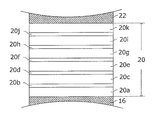
- FIG. 2 is a cross-sectional view schematically showing an enlarged view of the light emitting layer 20 and the vicinity thereof in the nitride semiconductor light emitting device 1.
- the light emitting layer 20 includes a barrier layer (20a, 20c, 20e, 20g, 20i, 20k) formed of a nitride semiconductor, and a well layer (20b, 20d, 20f, 20h, 20j) formed of a nitride semiconductor.
- a barrier layer (20a, 20c, 20e, 20g, 20i, 20k) formed of a nitride semiconductor and a well layer (20b, 20d, 20f, 20h, 20j) formed of a nitride semiconductor.
- the light emitting layer 20 is configured to have six barrier layers and five well layers, but the number of barrier layers and well layers is merely an example, and can be set as appropriate.
- the barrier layers (20a, 20c, 20e, 20g, 20i, 20k) are made of, for example, Al b Ga 1-b N (0 ⁇ b ⁇ 1), and the well layers (20b, 20d, 20f, 20h, 20j). ) Is formed of, for example, In c Ga 1-c N (0 ⁇ c ⁇ 1).
- the light emitting layer 20 is composed of well layers (20b, 20d, 20f, 20h, 20j) made of .97N.
- the nitride semiconductor light emitting device 1 is configured such that, of the barrier layers, the barrier layer 20k formed at a position in contact with the p-type nitride semiconductor layer 22, that is, the final barrier layer 20k includes at least an n-type impurity.
- the n-type impurity concentration at the interface with the p-type nitride semiconductor layer 22 is set to 4 ⁇ 10 17 / cm 3 or less.
- the characteristics of the device were evaluated by changing the n-type impurity concentration contained in the light emitting layer 10, particularly the barrier layers (20a, 20c, 20e, 20g, 20i, 20k).
- Example 1 All the barrier layers have a thickness of 20 nm and contain n-type impurities.
- the final barrier layer 20k has an n-type impurity concentration of 3 ⁇ 10 16 / at the interface with the p-type nitride semiconductor layer 22. It was formed to have a cm 3.
- TMG trimethylgallium
- TMA trimethylaluminum
- TESi Tetraethylsilane
- Si doped by the supply of TESi, that is, n-type impurities diffuses to the surface side of the final barrier layer 20k.
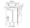
- FIG. 3 is a graph schematically showing an example of a result of composition analysis performed on the formed nitride semiconductor light emitting device using SIMS (Secondary Ion Mass Spectrometry).
- the axis represents the distance in the depth direction from the surface
- the right vertical axis represents the Al composition ratio
- the left vertical axis represents the Si concentration.
- FIG. 3 shows a case where analysis is performed on an element in which the p-type contact layer 26 is not formed in FIG.
- the composition When measuring the n-type impurity concentration using SIMS or the like, the composition is evaluated while etching at a predetermined pitch in the depth direction from the surface of the nitride semiconductor light emitting device.
- the composition ratio value obtained is a discrete value corresponding to the etching pitch.
- FIG. 3 schematically shows the results when the composition analysis at each measurement point is performed by SIMS while etching the device in the depth direction from the surface at a pitch of 5 nm.
- a signal derived from the p-type nitride semiconductor layer 22 (p-Al 0.3 Ga 0.7 N) formed under the p-type cladding layer 24 starts to be obtained. Since this layer has a higher Al composition ratio than the p-type cladding layer 24, the value of the Al composition is increased. On the other hand, since Si which is an n-type impurity is not included, the Si concentration value of 1 ⁇ 10 16 / cm 3 , which is a detection limit of the n-type impurity concentration, is shown in the same manner as the p-type cladding layer 24.
- the composition analysis is performed at each measurement point by performing etching at a pitch of 5 nm, the analysis result obtained on the graph is a discrete value. For this reason, the value of the composition ratio at the position between the measurement points cannot be obtained strictly. Therefore, as shown in FIG. 3, the composition values at the positions between the measurement points are also estimated by complementing the discrete values obtained at the measurement points with straight lines. When such a method is adopted, it can be said that the finer the etching pitch, the more accurate value is obtained, which is preferable.
- the pitch is 5 nm, but it is preferably 5 nm or less, and more preferably 2 nm or less.
- a signal derived from the final barrier layer 20k formed under the p-type nitride semiconductor layer 22 starts to be obtained. Since this final barrier layer 20k is formed of Al 0.08 Ga 0.92 N containing n-type impurities (Si), an Al signal and an Si signal can be obtained from the measurement points in the layer. . Regarding the Al composition ratio, since the final barrier layer 20k is smaller than the p-type nitride semiconductor layer 22, the numerical value thereof decreases. On the other hand, since Si is not included in the p-type nitride semiconductor layer 22 and is included in the final barrier layer 20k, the numerical value increases.
- the interface between the p-type nitride semiconductor layer 22 and the final barrier layer 20k may not be a measurement point. More specifically, the immediately preceding measurement point 22a is the closest point to the final barrier layer 20k in the p-type nitride semiconductor layer 22, and the immediately subsequent measurement point 20ka is the most p-type nitrided in the final barrier layer 20k. There is a possibility of being close to the physical semiconductor layer 22. In this case, in a strict sense, the n-type impurity concentration at the interface between the final barrier layer 20k and the p-type nitride semiconductor layer 22 cannot be measured.
- the Al composition difference between the final barrier layer 20k and the p-type nitride semiconductor layer 22 is halved at the interface between the final barrier layer 20k and the p-type nitride semiconductor layer 22.
- the Al composition decreases and the Si concentration increases from the p-type nitride semiconductor layer 22 toward the final barrier layer 20k. Therefore, the Al composition value at the measurement point 22a closest to the final barrier layer 20k in the p-type nitride semiconductor layer 22 and the Al composition value at the measurement point 20ka closest to the p-type nitride semiconductor layer 22 in the final barrier layer 20k. Is complemented by a straight line, and the position of the interface 21 between the final barrier layer 20k and the p-type nitride semiconductor layer 22 is derived at a location where the value becomes an intermediate value.
- the Si concentration value at the measurement point 22a closest to the final barrier layer 20k in the p-type nitride semiconductor layer 22 and the measurement closest to the p-type nitride semiconductor layer 22 in the final barrier layer 20k is derived.
- Example 1 when the final barrier layer 20k is formed, for the first approximately 120 seconds, TESi is supplied in addition to nitrogen, hydrogen, TMG, and TMA to grow 5 nm while containing n-type impurities. Thereafter, the supply of TESi was stopped, and nitrogen, hydrogen, TMG and TMA were supplied for growth for about 360 seconds, and finally, the final barrier layer 20k having a layer thickness of 20 nm was formed over about 480 seconds. As a result, the n-type impurity concentration at the interface with the p-type nitride semiconductor layer 22 in the final barrier layer 20k was set to 3 ⁇ 10 16 / cm 3 .
- the n-type impurity concentration at the interface between the final barrier layer 20k and the p-type nitride semiconductor layer 22 was measured by the above method.
- Example 2 When the final barrier layer 20k is formed, the TESi supply time is set to about 240 seconds to grow 10 nm while containing n-type impurities, and then the supply of TESi is stopped, and nitrogen, hydrogen, TMG, and TMA are stopped.
- the TESi supply time is set to about 240 seconds to grow 10 nm while containing n-type impurities, and then the supply of TESi is stopped, and nitrogen, hydrogen, TMG, and TMA are stopped.
- the n-type impurity concentration at the interface between the final barrier layer 20k and the p-type nitride semiconductor layer 22 was 7 ⁇ 10 16 / cm 3 .
- Example 3 An element was formed under the same conditions as in Example 2 except that some of the barrier layers 20g in the barrier layers (20a, 20c, 20e, 20g, 20i, 20k) were undoped.
- Example 4 When the final barrier layer 20k is formed, the TESi supply time is set to about 288 seconds to grow 12 nm while containing n-type impurities, and then the supply of TESi is stopped and nitrogen, hydrogen, TMG, and TMA are stopped. Was supplied and grown for about 192 seconds, so that the final barrier layer 20k having a layer thickness of 20 nm was finally formed over about 480 seconds. Thereby, in the element of Example 4, the n-type impurity concentration at the interface between the final barrier layer 20k and the p-type nitride semiconductor layer 22 was 1.5 ⁇ 10 17 / cm 3 .
- Example 5 When the final barrier layer 20k is formed, the TESi supply time is set to about 360 seconds, and after growth of 15 nm while containing n-type impurities, the supply of TESi is stopped and nitrogen, hydrogen, TMG, and TMA are stopped. Was supplied for about 120 seconds to grow, and was formed in the same manner as in Example 1 except that the final barrier layer 20k having a layer thickness of 20 nm was finally formed over about 480 seconds. Thereby, in the element of Example 5, the n-type impurity concentration at the interface between the final barrier layer 20k and the p-type nitride semiconductor layer 22 was 4 ⁇ 10 17 / cm 3 .
- the TESi supply time is set to about 456 seconds to grow 19 nm while containing n-type impurities. Then, the supply of TESi is stopped, and nitrogen, hydrogen, TMG, and TMA are stopped. Was supplied and grown for about 24 seconds, so that the final barrier layer 20k having a layer thickness of 20 nm was finally formed over about 480 seconds. Thereby, in the element of Comparative Example 1, the n-type impurity concentration at the interface between the final barrier layer 20k and the p-type nitride semiconductor layer 22 was 8 ⁇ 10 17 / cm 3 .
- FIG. 4 is a graph showing the relationship between the amount of light emitted from each element of Examples 1 to 5 and Comparative Examples 1 and 2 and the supply current.
- the n-type impurity concentration hereinafter, abbreviated as “interface concentration” where appropriate
- interface concentration at the interface between the final barrier layer 20k and the p-type nitride semiconductor layer 22 is set to 7 ⁇ 10 16 / cm 3.
- 2 has the highest light emission amount, and the light emission amount is in the order of Example 1 in which the interface concentration is 3 ⁇ 10 16 / cm 3 and Example 4 in which the interface concentration is 1.5 ⁇ 10 17 / cm 3. I understand that it is expensive.
- Example 3 In Example 3 in which the interface concentration was set to 7 ⁇ 10 16 / cm 3 and some of the barrier layers (20 g) were undoped, all barrier layers were doped with n-type impurities under the same interface concentration. Although the amount of emitted light is lower than that of Example 2, the amount of emitted light is higher than that of Comparative Example 1 in which the final barrier layer 20k is undoped.
- Example 5 where the interface concentration was 4 ⁇ 10 17 / cm 3 , the amount of emitted light was lower than in Examples 1 to 4, but the amount of emitted light was also higher than that in Comparative Example 1 in which the final barrier layer 20 k was undoped.
- Comparative Example 2 in which the interface concentration is 8 ⁇ 10 17 / cm 3 , the amount of emitted light is lower than in Comparative Example 1 in which the final barrier layer 20 k is undoped.
- the final barrier layer 20k is doped with an n-type impurity, and the n-type impurity concentration at the interface between the final barrier layer 20k and the p-type nitride semiconductor layer 22 is 4 ⁇ 10 17 / cm 3 or less.
- the luminous efficiency is improved as compared with the conventional device in which the final barrier layer 20k is undoped.
- Example 2 and Example 3 are compared, the light emission efficiency is higher when all the barrier layers are doped with n-type impurities, but the interface between the final barrier layer 20k and the p-type nitride semiconductor layer 22 is increased.
- the n-type impurity concentration By setting the n-type impurity concentration to 4 ⁇ 10 17 / cm 3 or less, even if some of the barrier layers are undoped, the light emission efficiency can be improved over the conventional device in which the final barrier layer 20 k is undoped. I understand.
- FIG. 5 is a graph showing the results of evaluating the withstand voltage characteristics by applying a reverse bias voltage to the elements of Examples 1 to 5 and Comparative Examples 1 and 2.
- the horizontal axis indicates the interface concentration, and the vertical axis indicates the magnitude of the reverse bias voltage necessary for flowing a reverse bias current of 1 ⁇ A.
- the interface concentration is 1.5 ⁇ 10 16 , but this is a value associated with noise, which is a practical measurement limit, and may actually be undoped.
- TMA trimethylaluminum
- TMG trimethylgallium
- the compound is trimethylindium (TMI), the organometallic compound serving as the Si atom supply source is tetraethylsilane (TESi), and the organometallic compound serving as the Mg atom supply source is biscyclopentadienyl magnesium (Cp 2 Mg).
- TMI trimethylindium
- TESi tetraethylsilane
- Cp 2 Mg biscyclopentadienyl magnesium
- ammonia is used as the compound serving as the N atom supply source
- nitrogen gas and hydrogen gas are used as the carrier gas, but are not limited thereto.
- a c-plane sapphire substrate is prepared as the support substrate 10 and this cleaning is performed. More specifically, for example, a c-plane sapphire substrate is disposed in a processing furnace of a MOCVD (Metal Organic Chemical Vapor Deposition) apparatus, and hydrogen gas having a flow rate of 10 slm is flowed into the processing furnace. For example, the temperature in the furnace is increased to 1150 ° C.
- MOCVD Metal Organic Chemical Vapor Deposition
- Step S2> in a state where the furnace pressure is 100 kPa and the substrate temperature is 480 ° C., while supplying nitrogen gas as a carrier gas into the processing furnace at a flow rate of 5 slm and hydrogen gas at a flow rate of 5 slm, ammonia is supplied at a flow rate of 250,000 ⁇ mol / min and TMG is supplied at a flow rate of 50 ⁇ mol.
- a GaN layer having a thickness of 20 nm is grown on the surface of the support substrate 10 to form the first buffer layer (LT-GaN) 12.
- Step S3> in a state where the substrate temperature is 1150 ° C., while supplying nitrogen gas as a carrier gas into the processing furnace at a flow rate of 20 slm and hydrogen gas at a flow rate of 15 slm, ammonia is supplied at a flow rate of 250,000 ⁇ mol / min and TMG is supplied at a flow rate of 100 ⁇ mol / min for 30 minutes.
- an undoped GaN layer having a layer thickness of 1.7 ⁇ m is grown on the first buffer layer 12 to form a second buffer layer (u-GaN) 14.
- an n-type nitride semiconductor layer 16 composed of n-Al n Ga 1-n N (0 ⁇ n ⁇ 1) is formed on the second buffer layer 14. More specifically, as in step S3, while supplying nitrogen gas as a carrier gas into the processing furnace at a flow rate of 20 slm and hydrogen gas at a flow rate of 15 slm, the TMA is heated at a substrate temperature of 1150 ° C. and a furnace pressure of 30 kPa.
- a nitride semiconductor layer 16 is formed.
- Si is used as an n-type impurity as a dopant, but Ge, S, Se, Sn, Te, or the like can be used.
- Step S5> a well layer made of In c Ga 1-c N (0 ⁇ c ⁇ 1) and a barrier layer made of Al b Ga 1-b N (0 ⁇ b ⁇ 1) are formed on the n-type nitride semiconductor layer 16.
- a light emitting layer 20 is formed in which are alternately repeated.
- a more specific method for forming the light emitting layer 20 is, for example, as follows. After step S4, the growth process is interrupted. Then, while supplying nitrogen gas as a carrier gas into the processing furnace at a flow rate of 15 slm and hydrogen gas at a flow rate of 1 slm, the TMG is set at a furnace pressure of 100 kPa and a substrate temperature of 820 ° C. Is supplied at a flow rate of 10 ⁇ mol / min and TMI is supplied at a flow rate of 7 ⁇ mol / min for 120 seconds to form a well layer having a composition of In 0.03 Ga 0.97 N with a thickness of 5 nm, and TMG at a flow rate of 10 ⁇ mol / min.
- a barrier layer having a composition of n-Al 0.08 Ga 0.92 N with a layer thickness of 20 nm is formed.
- the process to do is performed.
- five layers of well layers and barrier layers are stacked.
- Si doping to the barrier layer may be performed on the entire barrier layer, or there is a possibility that the implantation efficiency may be reduced due to excessive Si entering the InGaN layer which is a well layer due to diffusion of Si. May partially dope the barrier layer.
- TMG is supplied at a flow rate of 10 ⁇ mol / min
- TMA is supplied at a flow rate of 0.9 ⁇ mol / min
- TESi is supplied at a flow rate of 0.9 ⁇ mol / min for a predetermined time, and then the supply of TESi is stopped.
- the final barrier layer 20k having a composition of n-Al 0.08 Ga 0.92 N with a layer thickness of 20 nm is formed. .
- the surface of the final barrier layer 20k that is, the n-type impurity at the interface of the p-type nitride semiconductor layer 22 formed in the next step S6 is reduced.
- the concentration can be 4 ⁇ 10 17 / cm 3 or less.
- Step S6> While supplying nitrogen gas as a carrier gas at a flow rate of 15 slm and hydrogen gas at a flow rate of 25 slm at a furnace pressure of 100 kPa, the substrate temperature is set to 1025 ° C. In this state, TMG is flowed at 100 ⁇ mol / min, and TMA is flowed at 24 ⁇ mol / By supplying min and Cp 2 Mg at a flow rate of 0.1 ⁇ mol / min for 20 seconds, a p-Al 0.3 Ga 0.7 N layer having a thickness of 20 nm is grown on the light emitting layer 20 to form a p-type nitride semiconductor. Layer 22 is formed.
- Step S7> Subsequently, by changing the flow rate of TMA to 12 ⁇ mol / min and continuing the growth for 100 seconds, p-Al 0.13 Ga 0.87 N having a layer thickness of 100 nm is formed on the p-type nitride semiconductor layer 22. A mold cladding layer 24 is formed.
- Step S8> After step S7, the flow rate of Cp 2 Mg is changed to 0.2 ⁇ mol / min and the growth is continued for 20 seconds, whereby p + type Al 0.1 Ga 0. A p-type contact layer 26 made of 9N is formed.
- Step S9 an activation process is performed on the wafer obtained through steps S1 to S8. More specifically, activation is performed in the atmosphere at 700 ° C. for 15 minutes using an RTA (Rapid Thermal Anneal) device.
- RTA Rapid Thermal Anneal
- an n-pad part is formed by etching and exposing a part of the n-type nitride semiconductor layer by photolithography and inductively coupled plasma processing apparatus (ICP), and the n-pad part and the p-type contact layer are formed.
- ICP photolithography and inductively coupled plasma processing apparatus
- an electrode material for example, Ni 5 nm and gold 5 nm
- annealing is performed in the atmosphere at a temperature of 500 ° C. for 5 minutes, and each of the n pad portion and the p pad portion is performed.
- Al is vapor-deposited to form an n-electrode and a p-electrode.
- an electrode material is laminated at a place where the support substrate 10 was present to form an n-electrode. Then, a p-electrode is formed on the p-pad portion set on the surface of the p-type contact layer 26 by the same method as described above.
- Nitride semiconductor light emitting element 10 Support substrate 12: 1st buffer layer 14: 2nd buffer layer 16: N-type nitride semiconductor layer 20: Light emitting layer 20a, 20c, 20e, 20g, 20i, 20k: Barrier layer 20b , 20d, 20f, 20h, 20j: well layer 20ka: measurement point closest to p-type nitride semiconductor layer 22 in final barrier layer 20k 21: interface between final barrier layer 20k and p-type nitride semiconductor layer 22: p Type nitride semiconductor layer 22a: measurement point closest to final barrier layer 20k in p type nitride semiconductor layer 22 24: p type cladding layer 26: p type contact layer
Landscapes
- Chemical & Material Sciences (AREA)
- General Chemical & Material Sciences (AREA)
- Chemical Kinetics & Catalysis (AREA)
- Engineering & Computer Science (AREA)
- Materials Engineering (AREA)
- Mechanical Engineering (AREA)
- Metallurgy (AREA)
- Organic Chemistry (AREA)
- Inorganic Chemistry (AREA)
- Led Devices (AREA)
- Semiconductor Lasers (AREA)
Abstract
Description
前記障壁層のうち前記p型窒化物半導体層と接する位置に形成される最終障壁層は、n型不純物を含み、前記p型窒化物半導体層との界面のn型不純物濃度が4×10¹⁷/cm3以下であることを特徴とする。
前記最終障壁層の形成時に、前記最終障壁層の材料を形成するための第1原料ガスに、n型不純物を含有させるための第2原料ガスを含有した混合ガスを供給する工程と、前記第2原料ガスの供給を停止して引き続き前記第1原料ガスを供給する工程とを含むことを特徴とする。
図1は、窒化物半導体発光素子の構造を模式的に示す断面図である。窒化物半導体発光素子1は、n型窒化物半導体層16とp型窒化物半導体層22の間に発光層20を有してなる構成である。より詳細には、窒化物半導体発光素子1は、サファイアなどの支持基板10の上層に、下から順に第1バッファ層12、第2バッファ層14、n型窒化物半導体層16、発光層20、p型窒化物半導体層22、p型クラッド層24、p型コンタクト層26を備える。
支持基板10は、サファイア基板で構成される。なお、サファイアの他、Si,SiC,GaN,YAGなどで構成しても構わない。
第1バッファ層12は、支持基板10(サファイア基板)のc面上で低温成長させたGaN層にて形成される。また、第2バッファ層14は、第1バッファ層12の上層に高温成長させた下地層としてのGaN層である。両層ともにアンドープ層を構成する。
n型窒化物半導体層16は、第2バッファ層14の上層に高温成長させたn-AlnGa1-nN(0≦n<1)で構成される。一例として、本実施形態ではn-Al0.06Ga0.94Nによってn型窒化物半導体層16を形成している。ドーパントとしてのn型不純物としてはSiが好適に用いられるが、Ge、S、Se、Sn、Teなどを用いることもできる。
p型窒化物半導体層22は、発光層20の上層に成長させたp-AlmGa1-mN(0≦m<1)で構成される。また、p型クラッド層24は、p型窒化物半導体層22の上層に成長させたp-AlaGa1-aN(0≦a<1)で構成される。一例として、本実施形態では、p-Al0.3Ga0.7Nによってp型窒化物半導体層22を形成し、p-Al0.13Ga0.87Nによってp型クラッド層24を形成している。ドーパントとしてのn型不純物としてはMgが好適に用いられるが、Be、Zn、Cなどを用いることもできる。
p型コンタクト層26は、p型クラッド層24の上層に成長させた、例えばp+-GaN又はp+-AlGaNで構成される。例えば、Mgが高濃度にドープされたGaN又はAlGaNで形成されるが、Be、Zn、Cなどを高濃度にドープして形成することもできる。
発光層20の構成について、図2を参照して説明する。図2は、窒化物半導体発光素子1のうち、発光層20及びその近傍の部分を拡大して模式的に示した断面図である。
図2に示す構成に関し、発光層10、特に障壁層(20a,20c,20e,20g,20i、20k)に含有させるn型不純物濃度を変更して、素子の特性の評価を行った。
全ての障壁層の厚みを20nmとして、これらに対してn型不純物を含有すると共に、最終障壁層20kに関しては、p型窒化物半導体層22との界面のn型不純物濃度が3×10¹⁶/cm3となるように形成した。
最終障壁層20kを形成するに際し、TESiの供給時間を約240秒間とすることでn型不純物を含有させながら10nmを成長させた後、TESiの供給を停止して、窒素、水素、TMG及びTMAを約240秒間供給して成長させることで、最終的に約480秒間をかけて層厚20nmの最終障壁層20kを形成した以外は、実施例1と同様に形成した。これにより、実施例2の素子において、最終障壁層20kとp型窒化物半導体層22の界面のn型不純物濃度は7×10¹⁶/cm3であった。
障壁層(20a,20c,20e,20g,20i、20k)のうちの一部の障壁層20gについてアンドープとした以外は、実施例2と同条件として素子を形成した。
最終障壁層20kを形成するに際し、TESiの供給時間を約288秒間とすることでn型不純物を含有させながら12nmを成長させた後、TESiの供給を停止して、窒素、水素、TMG及びTMAを約192秒間供給して成長させることで、最終的に約480秒間をかけて層厚20nmの最終障壁層20kを形成した以外は、実施例1と同様に形成した。これにより、実施例4の素子において、最終障壁層20kとp型窒化物半導体層22の界面のn型不純物濃度は1.5×10¹⁷/cm3であった。
最終障壁層20kを形成するに際し、TESiの供給時間を約360秒間とすることでn型不純物を含有させながら15nmを成長させた後、TESiの供給を停止して、窒素、水素、TMG及びTMAを約120秒間供給して成長させることで、最終的に約480秒間をかけて層厚20nmの最終障壁層20kを形成した以外は、実施例1と同様に形成した。これにより、実施例5の素子において、最終障壁層20kとp型窒化物半導体層22の界面のn型不純物濃度は4×10¹⁷/cm3であった。
TESiを供給せずに最終障壁層20kを形成したことで、最終障壁層20kをアンドープとした以外は、実施例1と同様に形成した。
最終障壁層20kを形成するに際し、TESiの供給時間を約456秒間とすることでn型不純物を含有させながら19nmを成長させた後、TESiの供給を停止して、窒素、水素、TMG及びTMAを約24秒間供給して成長させることで、最終的に約480秒間をかけて層厚20nmの最終障壁層20kを形成した以外は、実施例1と同様に形成した。これにより、比較例1の素子において、最終障壁層20kとp型窒化物半導体層22の界面のn型不純物濃度は8×10¹⁷/cm3であった。
以下、窒化物半導体発光素子1の製造方法の一例について説明する。なお、下記製造方法で説明する製造条件や膜厚などの寸法は、あくまで一例であって、これらの数値に限定されるものではない。すなわち、各半導体層の成長工程においては、目的とする組成に応じた基板温度および炉内圧力となる条件下で気相成長が行われるものとして構わない。
まず、支持基板10としてc面サファイア基板を準備し、このクリーニングを行う。より具体的には、例えばMOCVD(Metal Organic Chemical Vapor Deposition:有機金属化学気相蒸着)装置の処理炉内にc面サファイア基板を配置し、処理炉内に流量が10slmの水素ガスを流しながら、炉内温度を例えば1150℃に昇温することにより行われる。
次に、炉内圧力100kPa、基板温度480℃の状態で、処理炉内にキャリアガスとして窒素ガスを流量5slm及び水素ガスを流量5slmで供給しながら、アンモニアを流量250000μmol/min及びTMGを流量50μmol/minで70秒間供給することにより、支持基板10の表面に層厚20nmのGaN層を成長させて第1バッファ層(LT-GaN)12を形成する。
次に、基板温度1150℃の状態で、処理炉内にキャリアガスとして窒素ガスを流量20slm及び水素ガスを流量15slmで供給しながら、アンモニアを流量250000μmol/min及びTMGを流量100μmol/minで30分間供給することにより、第1バッファ層12上に層厚1.7μmのアンドープのGaN層を成長させて第2バッファ層(u-GaN)14を形成する。
次に、第2バッファ層14の上層に、n-AlnGa1-nN(0≦n<1)で構成されるn型窒化物半導体層16を形成する。より具体的には、ステップS3と同様に、処理炉内にキャリアガスとして窒素ガスを流量20slm及び水素ガスを流量15slmで供給しながら、基板温度1150℃、炉内圧力30kPaの状態で、TMAを流量5.2μmol/min、TESiを流量0.013μmol/minで供給することにより、第2バッファ層14上に層厚2.3μmのn-Al0.06Ga0.94N層よりなるn型窒化物半導体層16を形成する。
次に、n型窒化物半導体層16の上層にIncGa1-cN(0<c≦1)からなる井戸層とAlbGa1-bN(0<b≦1)からなる障壁層が交互に繰り返されてなる発光層20を形成する。
炉内圧力100kPaで処理炉内にキャリアガスとして窒素ガスを流量15slm及び水素ガスを流量25slmで供給しながら、基板温度を1025℃にし、その状態でTMGを流量100μmol/min、TMAを流量24μmol/min、Cp2Mgを流量0.1μmol/minで20秒間供給することにより、発光層20上に層厚20nmのp-Al0.3Ga0.7N層を成長させてp型窒化物半導体層22を形成する。
続いて、TMAの流量を12μmol/minに変更して成長を100秒間継続することにより、p型窒化物半導体層22上に層厚100nmのp-Al0.13Ga0.87Nよりなるp型クラッド層24を形成する。
ステップS7の後、Cp2Mgの流量を0.2μmol/minに変更して成長を20秒間継続することにより、p型クラッド層24上に層厚20nmのp+型Al0.1Ga0.9Nよりなるp型コンタクト層26を形成する。
次に、ステップS1~S8を経て得られたウェハに対して活性化処理を行う。より具体的には、RTA(Rapid Thermal Anneal:急速加熱)装置を用いて、大気中700℃で15分間の活性化処理を行う。
その後は、フォトリソグラフィと誘導結合型プラズマ処理装置(ICP)により、n型窒化物半導体層の一部をエッチングして露出させることによりnパッド部を形成し、当該nパッド部及びp型コンタクト層26の表面に設定されたpパッド部の各々に、電極材料(例えばNi5nm及び金5nm)を形成後、大気中において温度500℃で5分間アニールを行い、nパッド部及びpパッド部の各々にAlを蒸着してn電極及びp電極を形成する。
10 : 支持基板
12 : 第1バッファ層
14 : 第2バッファ層
16 : n型窒化物半導体層
20 : 発光層
20a,20c,20e,20g,20i、20k : 障壁層
20b,20d,20f,20h,20j : 井戸層
20ka : 最終障壁層20kにおける最もp型窒化物半導体層22に近い測定点
21 : 最終障壁層20kとp型窒化物半導体層22との界面
22 : p型窒化物半導体層
22a : p型窒化物半導体層22における最も最終障壁層20kに近い測定点
24 : p型クラッド層
26 : p型コンタクト層
Claims (3)
- n型窒化物半導体層とp型窒化物半導体層との間に、窒化物半導体からなる井戸層と窒化物半導体からなる障壁層とを交互に積層してなる発光層を有する窒化物半導体発光素子であって、
前記障壁層のうち前記p型窒化物半導体層と接する位置に形成される最終障壁層は、n型不純物を含み、前記p型窒化物半導体層との界面のn型不純物濃度が4×10¹⁷/cm3以下であることを特徴とする窒化物半導体発光素子。 - 前記最終障壁層を含む全ての前記障壁層が、n型不純物を含む構成であることを特徴とする請求項1に記載の窒化物半導体発光素子。
- 請求項1に記載の窒化物半導体発光素子の製造方法であって、
前記最終障壁層の形成時に、前記最終障壁層の材料を形成するための第1原料ガスに、n型不純物を含有させるための第2原料ガスを含有した混合ガスを供給する工程と、前記第2原料ガスの供給を停止して引き続き前記第1原料ガスを供給する工程とを含むことを特徴とする窒化物半導体発光素子の製造方法。
Priority Applications (2)
| Application Number | Priority Date | Filing Date | Title |
|---|---|---|---|
| US14/906,704 US20160163928A1 (en) | 2013-07-23 | 2014-06-16 | Nitride semiconductor light emitting element and method for manufacturing the same |
| KR1020157034271A KR101692181B1 (ko) | 2013-07-23 | 2014-06-16 | 질화물 반도체 발광소자 및 그 제조 방법 |
Applications Claiming Priority (2)
| Application Number | Priority Date | Filing Date | Title |
|---|---|---|---|
| JP2013152571A JP5858246B2 (ja) | 2013-07-23 | 2013-07-23 | 窒化物半導体発光素子及びその製造方法 |
| JP2013-152571 | 2013-07-23 |
Publications (1)
| Publication Number | Publication Date |
|---|---|
| WO2015012017A1 true WO2015012017A1 (ja) | 2015-01-29 |
Family
ID=52393070
Family Applications (1)
| Application Number | Title | Priority Date | Filing Date |
|---|---|---|---|
| PCT/JP2014/065906 Ceased WO2015012017A1 (ja) | 2013-07-23 | 2014-06-16 | 窒化物半導体発光素子及びその製造方法 |
Country Status (5)
| Country | Link |
|---|---|
| US (1) | US20160163928A1 (ja) |
| JP (1) | JP5858246B2 (ja) |
| KR (1) | KR101692181B1 (ja) |
| TW (1) | TWI602321B (ja) |
| WO (1) | WO2015012017A1 (ja) |
Cited By (1)
| Publication number | Priority date | Publication date | Assignee | Title |
|---|---|---|---|---|
| JP7448626B1 (ja) | 2022-12-23 | 2024-03-12 | 日機装株式会社 | 窒化物半導体発光素子の製造方法 |
Families Citing this family (3)
| Publication number | Priority date | Publication date | Assignee | Title |
|---|---|---|---|---|
| KR102340717B1 (ko) * | 2015-06-23 | 2021-12-17 | 쑤저우 레킨 세미컨덕터 컴퍼니 리미티드 | 발광소자 및 그 제조방법 |
| CN105374912B (zh) * | 2015-10-28 | 2017-11-21 | 厦门市三安光电科技有限公司 | 发光二极管及其制作方法 |
| US12059575B2 (en) * | 2016-11-14 | 2024-08-13 | The Charles Stark Draper Laboratory, Inc. | Compliant optrodes for monitoring and stimulating biological tissue with patterned light |
Citations (5)
| Publication number | Priority date | Publication date | Assignee | Title |
|---|---|---|---|---|
| JP2010093186A (ja) * | 2008-10-10 | 2010-04-22 | Showa Denko Kk | 窒化ガリウム系化合物半導体発光素子の製造方法、窒化ガリウム系化合物半導体素子の積層構造及び窒化ガリウム系化合物半導体発光素子、並びにランプ |
| JP2011023539A (ja) * | 2009-07-15 | 2011-02-03 | Sumitomo Electric Ind Ltd | Iii族窒化物半導体光素子 |
| JP2011091251A (ja) * | 2009-10-23 | 2011-05-06 | Nichia Corp | 窒化物半導体発光素子 |
| JP2012069988A (ja) * | 2011-11-29 | 2012-04-05 | Toshiba Corp | 半導体発光素子及びその製造方法 |
| JP2013012683A (ja) * | 2011-06-30 | 2013-01-17 | Sharp Corp | 窒化物半導体発光素子およびその製造方法 |
Family Cites Families (6)
| Publication number | Priority date | Publication date | Assignee | Title |
|---|---|---|---|---|
| JPH11298090A (ja) | 1998-04-09 | 1999-10-29 | Nichia Chem Ind Ltd | 窒化物半導体素子 |
| TWI360891B (en) * | 2007-04-09 | 2012-03-21 | Epistar Corp | Light emitting device |
| CN102760796B (zh) * | 2011-04-29 | 2015-01-21 | 清华大学 | 发光二极管的制备方法 |
| JP5948776B2 (ja) * | 2011-09-27 | 2016-07-06 | ソニー株式会社 | 発光素子及びその製造方法 |
| KR20130058406A (ko) * | 2011-11-25 | 2013-06-04 | 삼성전자주식회사 | 반도체 발광소자 |
| TWI524551B (zh) * | 2012-11-19 | 2016-03-01 | 新世紀光電股份有限公司 | 氮化物半導體結構及半導體發光元件 |
-
2013
- 2013-07-23 JP JP2013152571A patent/JP5858246B2/ja active Active
-
2014
- 2014-05-29 TW TW103118814A patent/TWI602321B/zh active
- 2014-06-16 KR KR1020157034271A patent/KR101692181B1/ko active Active
- 2014-06-16 WO PCT/JP2014/065906 patent/WO2015012017A1/ja not_active Ceased
- 2014-06-16 US US14/906,704 patent/US20160163928A1/en not_active Abandoned
Patent Citations (5)
| Publication number | Priority date | Publication date | Assignee | Title |
|---|---|---|---|---|
| JP2010093186A (ja) * | 2008-10-10 | 2010-04-22 | Showa Denko Kk | 窒化ガリウム系化合物半導体発光素子の製造方法、窒化ガリウム系化合物半導体素子の積層構造及び窒化ガリウム系化合物半導体発光素子、並びにランプ |
| JP2011023539A (ja) * | 2009-07-15 | 2011-02-03 | Sumitomo Electric Ind Ltd | Iii族窒化物半導体光素子 |
| JP2011091251A (ja) * | 2009-10-23 | 2011-05-06 | Nichia Corp | 窒化物半導体発光素子 |
| JP2013012683A (ja) * | 2011-06-30 | 2013-01-17 | Sharp Corp | 窒化物半導体発光素子およびその製造方法 |
| JP2012069988A (ja) * | 2011-11-29 | 2012-04-05 | Toshiba Corp | 半導体発光素子及びその製造方法 |
Cited By (1)
| Publication number | Priority date | Publication date | Assignee | Title |
|---|---|---|---|---|
| JP7448626B1 (ja) | 2022-12-23 | 2024-03-12 | 日機装株式会社 | 窒化物半導体発光素子の製造方法 |
Also Published As
| Publication number | Publication date |
|---|---|
| KR20160003245A (ko) | 2016-01-08 |
| TW201523920A (zh) | 2015-06-16 |
| KR101692181B1 (ko) | 2017-01-02 |
| JP5858246B2 (ja) | 2016-02-10 |
| JP2015023238A (ja) | 2015-02-02 |
| TWI602321B (zh) | 2017-10-11 |
| US20160163928A1 (en) | 2016-06-09 |
Similar Documents
| Publication | Publication Date | Title |
|---|---|---|
| US12507504B2 (en) | Group III nitride semiconductor light-emitting element and method of manufacturing same | |
| KR102494071B1 (ko) | 발광 소자 및 그것을 제조하는 방법 | |
| TWI683448B (zh) | Iii族氮化物半導體發光元件及其製造方法 | |
| US10283671B2 (en) | Method of producing III nitride semiconductor light-emitting device | |
| CN102668138B (zh) | 氮化物半导体发光元件及其制造方法 | |
| CN102738329A (zh) | 第iii族氮化物半导体发光器件 | |
| CN112753108A (zh) | Iii族氮化物半导体发光元件及其制造方法 | |
| US20130307001A1 (en) | n-AlGaN THIN FILM AND ULTRAVIOLET LIGHT EMITTING DEVICE INCLUDING THE SAME | |
| JP5858246B2 (ja) | 窒化物半導体発光素子及びその製造方法 | |
| JP6725242B2 (ja) | 半導体発光素子およびその製造方法 | |
| TWI666790B (zh) | Iii族氮化物半導體發光元件的製造方法及iii族氮化物半導體發光元件 | |
| WO2007091637A1 (ja) | 半導体発光素子およびその製造方法 | |
| KR102359845B1 (ko) | 발광 소자 및 그것을 제조하는 방법 | |
| JP5800251B2 (ja) | Led素子 | |
| KR20130015112A (ko) | 발광 다이오드 및 그것을 제조하는 방법 | |
| JP2014146684A (ja) | 半導体発光素子及びその製造方法 | |
| JP5800252B2 (ja) | Led素子 | |
| JP2017117845A (ja) | 半導体発光素子およびその製造方法 | |
| JP2025098661A (ja) | 紫外半導体発光素子及びその製造方法 | |
| JP6478685B2 (ja) | 半導体発光素子 |
Legal Events
| Date | Code | Title | Description |
|---|---|---|---|
| 121 | Ep: the epo has been informed by wipo that ep was designated in this application |
Ref document number: 14829370 Country of ref document: EP Kind code of ref document: A1 |
|
| ENP | Entry into the national phase |
Ref document number: 20157034271 Country of ref document: KR Kind code of ref document: A |
|
| WWE | Wipo information: entry into national phase |
Ref document number: 14906704 Country of ref document: US |
|
| NENP | Non-entry into the national phase |
Ref country code: DE |
|
| 122 | Ep: pct application non-entry in european phase |
Ref document number: 14829370 Country of ref document: EP Kind code of ref document: A1 |