WO2015011894A1 - 放射線撮影装置 - Google Patents
放射線撮影装置 Download PDFInfo
- Publication number
- WO2015011894A1 WO2015011894A1 PCT/JP2014/003731 JP2014003731W WO2015011894A1 WO 2015011894 A1 WO2015011894 A1 WO 2015011894A1 JP 2014003731 W JP2014003731 W JP 2014003731W WO 2015011894 A1 WO2015011894 A1 WO 2015011894A1
- Authority
- WO
- WIPO (PCT)
- Prior art keywords
- radiation
- detection panel
- radiation detection
- imaging apparatus
- rigidity
- Prior art date
- Legal status (The legal status is an assumption and is not a legal conclusion. Google has not performed a legal analysis and makes no representation as to the accuracy of the status listed.)
- Ceased
Links
Images

Classifications
-
- G—PHYSICS
- G01—MEASURING; TESTING
- G01J—MEASUREMENT OF INTENSITY, VELOCITY, SPECTRAL CONTENT, POLARISATION, PHASE OR PULSE CHARACTERISTICS OF INFRARED, VISIBLE OR ULTRAVIOLET LIGHT; COLORIMETRY; RADIATION PYROMETRY
- G01J1/00—Photometry, e.g. photographic exposure meter
- G01J1/42—Photometry, e.g. photographic exposure meter using electric radiation detectors
- G01J1/44—Electric circuits
-
- G—PHYSICS
- G01—MEASURING; TESTING
- G01J—MEASUREMENT OF INTENSITY, VELOCITY, SPECTRAL CONTENT, POLARISATION, PHASE OR PULSE CHARACTERISTICS OF INFRARED, VISIBLE OR ULTRAVIOLET LIGHT; COLORIMETRY; RADIATION PYROMETRY
- G01J1/00—Photometry, e.g. photographic exposure meter
- G01J1/02—Details
- G01J1/0214—Constructional arrangements for removing stray light
-
- G—PHYSICS
- G01—MEASURING; TESTING
- G01J—MEASUREMENT OF INTENSITY, VELOCITY, SPECTRAL CONTENT, POLARISATION, PHASE OR PULSE CHARACTERISTICS OF INFRARED, VISIBLE OR ULTRAVIOLET LIGHT; COLORIMETRY; RADIATION PYROMETRY
- G01J1/00—Photometry, e.g. photographic exposure meter
- G01J1/02—Details
- G01J1/0271—Housings; Attachments or accessories for photometers
-
- G—PHYSICS
- G01—MEASURING; TESTING
- G01J—MEASUREMENT OF INTENSITY, VELOCITY, SPECTRAL CONTENT, POLARISATION, PHASE OR PULSE CHARACTERISTICS OF INFRARED, VISIBLE OR ULTRAVIOLET LIGHT; COLORIMETRY; RADIATION PYROMETRY
- G01J1/00—Photometry, e.g. photographic exposure meter
- G01J1/42—Photometry, e.g. photographic exposure meter using electric radiation detectors
-
- G—PHYSICS
- G01—MEASURING; TESTING
- G01J—MEASUREMENT OF INTENSITY, VELOCITY, SPECTRAL CONTENT, POLARISATION, PHASE OR PULSE CHARACTERISTICS OF INFRARED, VISIBLE OR ULTRAVIOLET LIGHT; COLORIMETRY; RADIATION PYROMETRY
- G01J1/00—Photometry, e.g. photographic exposure meter
- G01J1/58—Photometry, e.g. photographic exposure meter using luminescence generated by light
-
- G—PHYSICS
- G01—MEASURING; TESTING
- G01T—MEASUREMENT OF NUCLEAR OR X-RADIATION
- G01T1/00—Measuring X-radiation, gamma radiation, corpuscular radiation, or cosmic radiation
- G01T1/16—Measuring radiation intensity
- G01T1/24—Measuring radiation intensity with semiconductor detectors
-
- G—PHYSICS
- G21—NUCLEAR PHYSICS; NUCLEAR ENGINEERING
- G21F—PROTECTION AGAINST X-RADIATION, GAMMA RADIATION, CORPUSCULAR RADIATION OR PARTICLE BOMBARDMENT; TREATING RADIOACTIVELY CONTAMINATED MATERIAL; DECONTAMINATION ARRANGEMENTS THEREFOR
- G21F1/00—Shielding characterised by the composition of the materials
-
- G—PHYSICS
- G01—MEASURING; TESTING
- G01J—MEASUREMENT OF INTENSITY, VELOCITY, SPECTRAL CONTENT, POLARISATION, PHASE OR PULSE CHARACTERISTICS OF INFRARED, VISIBLE OR ULTRAVIOLET LIGHT; COLORIMETRY; RADIATION PYROMETRY
- G01J1/00—Photometry, e.g. photographic exposure meter
- G01J1/02—Details
- G01J2001/0276—Protection
Definitions
- the present invention relates to a radiation imaging apparatus.
- a device that irradiates an object with radiation and detects the intensity distribution of the radiation that has passed through the object to obtain a radiation image of the object has been widely used in industrial nondestructive inspection and medical diagnosis.
- an apparatus for photographing a digital radiation image has been developed by using a radiation detection panel that makes radiation incident on a phosphor as disclosed in Patent Document 1 and converts the emitted light into electrical information by a semiconductor sensor. The output image can be obtained immediately.
- a radiation detection panel for injecting radiation from the semiconductor sensor side as disclosed in Patent Document 2 has been proposed with the aim of improving image quality.
- Such an imaging apparatus is assumed to be subjected to an impact force such as a drop or an external force during imaging. Even in such a situation, in order for the radiation detection function inside the imaging apparatus to function normally, the imaging apparatus is required to take into account strength, vibration resistance, and impact resistance. In particular, depending on the method of capturing a radiographic image, a large pressure may be applied to the upper surface of the housing, which is the radiation incident surface of the housing. At that time, there is a high possibility that the glass substrate constituting the radiation detection panel is damaged. If the glass substrate is damaged, it is extremely difficult to take a suitable radiographic image, so that sufficient protection is required to avoid damage to the glass substrate. At the same time, the photographing apparatus is required to be small, thin, and lightweight in order to facilitate handling, improve portability, and enable rapid photographing.
- the radiation imaging apparatus may have various configurations.
- the upper surface of the housing which is the surface on which the radiation of the housing in which the radiation detection panel is housed is incident, has a relatively low rigidity and can be displaced. It consists of.
- the upper surface of the housing is displaced in a space provided between the upper surface of the housing and the radiation detection panel, thereby preventing the transmission of the shock to the radiation conversion panel or mitigating it.
- Patent Document 7 In order to protect the radiation detection panel from an impact force from the outside of the imaging apparatus, a structure is adopted in which a cushioning material that is difficult to be reflected as an artifact in the captured image is disposed between the radiation detection panel and the housing. There are cases (Patent Document 7).
- Patent Document 3 since it is assumed that the upper surface of the housing is freely displaced, a structure in which the thickness of the photographing apparatus is likely to increase is obtained.
- Patent Document 4 Patent Document 5, and Patent Document 6, it is necessary to ensure the necessary rigidity on the upper surface of the housing, which is the radiation incident surface of the housing.
- the radiation emitted from the radiation generation apparatus is detected by the radiation detection panel after passing through the subject and the upper surface of the housing.
- the upper surface of the housing is often a simple plate-like shape having a uniform thickness so as not to remain as an artifact in the photographed image.
- a buffer material is disposed between the radiation detection panel and the upper surface of the casing in order to reduce external force applied to the imaging unit.
- merely arranging the buffer material does not necessarily have a suitable structural relationship for protecting the radiation detection panel.
- the radiation imaging apparatus is required to be lightweight, and at the same time, the radiation detection panel is sufficiently affected by an external force load during use or an impact force such as dropping. Protection is also important.
- the present invention provides a radiation imaging apparatus capable of reducing the weight while protecting the radiation detection panel and ensuring the rigidity of the radiation imaging apparatus in view of the above circumstances.
- a radiographic apparatus is: A radiation detection panel for detecting radiation emitted from the radiation generating means; A first member and a second member arranged on the incident direction side of the radiation; A third member and a fourth member disposed on opposite sides of the incident direction of the radiation; With The second member is disposed between the first member and the radiation detection panel, The third member is disposed between the radiation detection panel and the fourth member; The elastic modulus of the second member and the third member is lower than the elastic modulus of the first member and the fourth member, The elastic modulus of the second member is equal to or lower than the elastic modulus of the third member.
- the present invention it is possible to provide a radiation imaging apparatus capable of reducing the weight while protecting the radiation detection panel and ensuring the rigidity of the radiation imaging apparatus.
- the accompanying drawings are included in the specification, constitute a part thereof, show an embodiment of the present invention, and are used to explain the principle of the present invention together with the description.
- the longitudinal cross-sectional view of 2nd Embodiment of a radiography apparatus The figure which shows the destructive load of the radiation detection panel 1 by the difference in a structure. The figure which showed a mode that a load was loaded with respect to the radiation detection panel 1.
- FIG. The figure which shows the state of the load of the stress of the glass member which comprises the radiation detection panel 1 by the difference in a structure.
- the longitudinal cross-sectional view of 3rd Embodiment of a radiography apparatus The longitudinal cross-sectional view of 3rd Embodiment of a radiography apparatus.
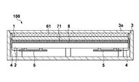
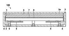
- FIG. 1 is a cross-sectional view illustrating a configuration example of a radiation imaging apparatus 100 according to the first embodiment.
- the radiation imaging apparatus 100 includes a radiation detection panel 1 and a control board 5 that processes data detected by the radiation detection panel 1.
- Control part is built in.
- the radiation imaging apparatus 100 detects radiation irradiated by a radiation generator (not shown) and transmitted through a subject with semiconductor elements arranged in a two-dimensional lattice pattern. An image acquired by the radiation imaging apparatus 100 is transferred to an external control apparatus (information processing apparatus), and the image transferred to the control apparatus is displayed on a monitor and used for diagnosis or the like.
- control board 5 is connected to the radiation detection panel 1 by the flexible circuit board 4, and performs read-out control of the radiation detection panel 1 and processing of electrical output.
- the radiation detection panel 1 and the control board 5 are supported by the base 2 and are arranged inside the radiation imaging apparatus 100.
- the radiation detection panel 1 is mainly composed of a glass substrate, a semiconductor element, a phosphor, a phosphor protective film, and the like.
- the radiation detection panel 1 has a so-called back-surface incidence configuration in which a glass substrate, a semiconductor element, a phosphor, and a phosphor protective film are arranged in this order from the radiation incident direction. With the back-illuminated configuration, the light emitting position of the phosphor and the position of the semiconductor element are close to each other, so that an image with high resolution can be obtained.
- an embodiment in which the present invention is effectively used may be a so-called surface incidence configuration in which a phosphor protective film, a phosphor, a semiconductor element, and a glass substrate are arranged in this order from the radiation incident direction.
- Such a radiation imaging apparatus 100 is assumed to be subjected to an impact force such as a drop or an external force during imaging. Even in such a situation, in order for the radiation detection function inside the radiation imaging apparatus 100 to function normally, the radiation imaging apparatus 100 is required to take into account strength, vibration resistance, and impact resistance.
- a patient or the like who captures the image is in contact with the radiation imaging apparatus 100, so that a large pressure is applied to the housing upper surface 3 a that is the radiation incident surface of the housing 3 that houses the radiation detection panel 1. May be granted.
- the housing upper surface 3a When pressure is applied to the housing upper surface 3a, the housing upper surface 3a is distorted by bending, and bending stress is generated.
- a bending stress is generated in the glass substrate as well.
- a large stress may be locally generated around the position where pressure is applied. At that time, there is a high possibility that the glass substrate constituting the radiation detection panel 1 is damaged.
- the stress generated from strain due to bending has a property that tensile stress is likely to be generated on the side opposite to the surface to which pressure is applied.
- a glass substrate tends to cause a breakage of tensile stress, and it is important to protect the glass to relax the tensile stress applied to the glass substrate. Therefore, it is necessary to adopt a structure in which the glass substrate is not distorted as much as possible or tensile stress is hardly generated even when pressure is applied from the upper surface of the housing.
- the radiation imaging apparatus 100 is required to be small, thin, and lightweight in order to facilitate handling, improve portability, and enable rapid imaging.
- the inside of the radiation imaging apparatus 100 has the following configuration. From the order of the radiation incident direction, the housing upper surface 3a (first member), the second component member 6 (second member), the radiation detection panel 1, and the third component member 7 which are the radiation incident surfaces of the housing. (Third member), radiation shielding member 8, and base 2 (fourth member).
- the housing upper surface 3 a (first member) and the second component member 6 (second member) are disposed on the radiation incident direction side with respect to the radiation detection panel 1.
- the third component member 7 (third member), the radiation shielding member 8, and the base 2 (fourth member) are disposed on the opposite side of the radiation incident direction with respect to the radiation detection panel 1. ing. With this configuration, it is possible to reduce the tensile stress applied to the radiation detection panel 1 by the force from the housing upper surface 3a side.
- the radiation detection panel 1 is lower than the rigidity of the housing upper surface 3a (first member) and the base 2 (fourth member).
- the impact on the radiation detection panel 1 can be further reduced by setting the second component member 6 and the third component member 7 to be equal to or larger than the area of the radiation detection panel 1 in the same manner.
- the second structural member 6 and the third structural member 7 have a lower elastic modulus than the housing upper surface 3 a, the radiation detection panel 1, and the base 2.
- the rigidity of the second component member 6 is equal to the rigidity of the third component member 7 or lower than the rigidity of the third component member 7.
- the elastic modulus of the second component member 6 is equal to or lower than the elastic modulus of the third component member 7.
- the third component member 7 is made of a material having an elastic modulus equal to that of the second component member 6 or higher than that of the second component member 6. That is, the elastic modulus of the third component member 7 is equal to or greater than the elastic modulus of the second component member 6 (the elastic modulus of the third component member ⁇ the elastic modulus of the second component member 6).
- a member having a small elastic modulus is more likely to be deformed than a member having a large elastic modulus.
- the elastic modulus of the second component member 6 is equal to or lower than the elastic modulus of the third component member 7, and the second component member 6 is connected to the third component member 7. It is easy to deform compared. Alternatively, the second component member 6 is easily deformed in the same manner as the third component member 7. Therefore, the deformation of the housing upper surface 3a and the like with respect to the load applied from the outside is absorbed by the deformation of the second component member 6, so that the influence of the deformation is prevented from reaching the radiation detection panel 1, and the radiation detection panel 1 is Can be protected.
- the plate thickness of the second component member 6 is equal to the plate thickness of the third component member 7 or the plate of the third component member 7 It is thicker than the thickness.
- the elastic modulus of the second component member 6 is equal to or lower than the elastic modulus of the third component member 7.
- the 2nd component member 6 and the 3rd component member 7 are comprised with the shock absorbing material.
- an elastic material such as rubber, foam, elastomer, or gel can be used.
- an elastic material such as rubber, foam, elastomer, or gel can be used as in the second component member 6. If there is, it is not limited to it.
- the upper surface 3a of the housing can be made of carbon fiber reinforced plastic (CFRP) or the like from the relationship between sufficient rigidity and radiation transmittance.
- CFRP carbon fiber reinforced plastic
- the base 2 since the base 2 needs to have sufficient rigidity, it is a structure having high rigidity such as fiber reinforced plastic such as CFRP, magnesium alloy, and aluminum alloy, and has higher rigidity than the upper surface 3a of the housing.
- the second constituent member 6 and the third constituent member 7 made of a material having a lower elastic modulus than the housing upper surface 3a and the like are expected to absorb the impact and deformation from the housing upper surface 3a and the like.
- the second structural member 6 is more easily distorted than the third structural member 7, so that the radiation detection panel 1 is less distorted.
- production of the tensile stress by distortion can be relieve
- damage to the radiation detection panel 1 can be reduced, the rigidity required for the radiation imaging apparatus 100 can be reduced, and the radiation imaging apparatus 100 can be reduced in weight and thickness.
- the third structural member 7 is more easily distorted than the second structural member 6 by changing the above-described structural relationship (the elastic modulus of the third structural member 7 ⁇ the elastic modulus of the second structural member 6).
- the relationship is as follows. In this case, although there is a function of relaxing the external force on the radiation detection panel 1, the radiation detection panel 1 can easily follow the strain and displacement of the third component member 7, so that the radiation detection panel 1 is loaded instead. It becomes the structure which is easy to start.
- a radiation shielding member 8 is disposed between the base 2 and the third component member 7.
- the radiation incident on the radiation imaging apparatus 100 is not completely absorbed by the phosphor constituting the radiation detection panel 1, but a part of the radiation passes through the radiation imaging apparatus 100 and is emitted to the outside of the radiation imaging apparatus 100.
- the radiation that has passed through the radiation imaging apparatus 100 is scattered on the wall surface or floor of the back surface, it may return to the radiation imaging apparatus 100 and enter the radiation detection panel 1. Since the difference in transmittance due to such a structure of scattered radiation is reflected as an image, it is necessary to suppress it as much as possible.
- the radiation shielding member 8 uses, for example, a material containing at least one heavy metal of lead (Pb), barium (Ba), tantalum (Ta), molybdenum (Mo), tungsten (W), or stainless steel. Can be configured.
- the radiation detection panel 1 can be protected from impact and deformation due to external force if the structural relationship (mechanical relationship) of the members around the radiation detection panel 1 is satisfied.
- the highly rigid structure does not necessarily need to be the housing upper surface 3a and the base 2.
- the structure which can reduce the load to glass can be taken compared with the past, the weight reduction and thickness reduction of the radiography apparatus 100 are attained.
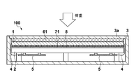
- FIG. 2 is a cross-sectional view illustrating a configuration example of the radiation imaging apparatus 100 according to the second embodiment.
- the radiation detection panel 1 is supported by the base 2.
- a control board 5 that performs readout control of the radiation detection panel 1 and processing of electrical output is connected to the radiation detection panel 1 by a flexible circuit board 4.
- the radiation detection panel 1 may have a so-called front incidence configuration or a back incidence configuration.
- the radiation imaging apparatus 100 includes a casing that is a radiation incident surface of the radiation detection panel 1 and the casing 3 that covers the radiation detection panel 1.
- attaches the body upper surface 3a is taken.
- the rigidity of the radiation imaging apparatus 100 is improved, and the base 2 that supports the radiation detection panel 1 may be omitted.
- the base 2 By omitting the base 2, there is an aspect in which a space for arranging the control board 5 is increased, and further, a configuration aiming at weight reduction becomes possible.
- the radiation imaging apparatus 100 it is assumed that a large load is applied to the upper surface 3a of the housing by an imaging method. Therefore, if the base 2 is omitted, a strong tensile stress is applied to the radiation detection panel 1 when an external force is applied to the upper surface 3a of the casing due to the layer configuration and the neutral axis of the bending stress. This tensile stress tends to cause a breakage of the glass substrate constituting the radiation detection panel 1.
- the radiation detection panel 1 is not arranged under a suitable structural relationship, there is a concern that a strong tensile stress is applied to the radiation detection panel 1, and the radiation detection panel 1 becomes a structure that is difficult to protect.
- the radiation detection panel 1 in the bonding structure in which the radiation detection panel 1 is bonded to the housing upper surface 3a, it is necessary to maintain high rigidity on the housing upper surface 3a or the like in order to maintain the rigidity required as a whole. .
- the radiation irradiated from the radiation generator is detected by the radiation detection panel 1 after passing through the subject and the upper surface 3a of the housing.
- the upper surface 3a of the casing is often a simple plate having a uniform thickness so as not to remain as an artifact in the photographed image.
- the radiation detection panel 1 when the radiation detection panel 1 is bonded to and integrated with the upper surface 3a of the housing, when a load such as an external force is applied to the housing, the external force is easily transmitted to the radiation detection panel 1, and There is a concern that the load will increase.
- the periphery of the radiation detection panel 1 is as shown in FIG. Take the configuration.
- the radiation detection panel 1 is integrated with a member including a housing upper surface 3 a that is a radiation incident surface of the housing 3, a second component member 61, a third component member 71, and the base 2. Yes.
- the second structural member 61 disposed between the housing upper surface 3a and the radiation detection panel 1 and the third structural member 71 disposed between the radiation detection panel 1 and the base 2 are connected to the housing.
- a member having lower rigidity (elastic modulus) than the body upper surface 3a, the radiation detection panel 1, and the base 2 is used.
- the third component member 71 is made of a material having an elastic modulus equal to that of the second component member 61 or higher than that of the second component member 61 as compared with the second component member 61.
- the elastic modulus of the second component member 61 is equal to the elastic modulus of the third component member 71 or lower than the elastic modulus of the third component member 71.
- the plate thickness of the second component member 61 is equal to the plate thickness of the third component member 71 or thicker than the plate thickness of the third component member 71.
- the thickness of the third component member 71 is made thinner than the thickness of the second component member 61.
- the rigidity of the base 2 is larger than the rigidity of the housing upper surface 3a.
- the second component member 61 disposed between the housing upper surface 3a and the radiation detection panel 1 can be integrated with the housing upper surface 3a and the radiation detection panel 1 in an elastic material such as rubber, foam, elastomer, or gel. Further, it can be constituted by a member in which a double-sided tape or an adhesive is disposed on both sides. Further, the third constituent member 71 disposed between the radiation detection panel 1 and the base 2 that supports the radiation detection panel 1 is the same as the second constituent member 61, and is elastic such as rubber, foam, elastomer, and gel. It can be composed of a material or a member such as a double-sided tape or an adhesive. The third component 71 may be any material that satisfies the mechanical relationship described above, for example.
- CFRP or the like can be used for the upper surface 3a of the housing from the relationship between sufficient rigidity and radiation transmittance. Furthermore, since the base 2 needs to give sufficient rigidity, it is a structure having high rigidity such as carbon fiber reinforced plastic such as CFRP, magnesium alloy, and aluminum alloy, and has higher rigidity than the housing upper surface 3a.
- the radiation detection panel 1 is integrated with the housing upper surface 3a and the base 2. With such a configuration, when an external force is applied to the upper surface 3a of the casing from the radiation incident direction with respect to the glass substrate constituting the radiation detection panel 1, it is easy to relieve the tensile stress that tends to cause the glass to break. It has been found by the present inventors.
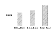
- FIG. 3 shows the relationship of the average external force that damages the radiation detection panel 1 when a load is applied to the radiation detection panel 1 due to the difference in thickness between the second component member 61 and the third component member 71.
- FIG. 4 Only the thicknesses of the second component member 61 and the third component member 71 are changed without changing the conditions regarding the housing upper surface 3a, the base 2, and the radiation detection panel 1.
- the second constituent member 61 and the third constituent member 71 use the same material.
- the load is applied from the radiation incident direction. This is because the radiation imaging apparatus 100 is likely to apply a high load from the radiation incident direction depending on the imaging method.
- the thicknesses of the two members are ⁇ and ⁇ , and ⁇ ⁇ .
- the second constituent member 61 having a thickness ⁇ is represented as second ( ⁇ ), and the second constituent member 61 having a thickness ⁇ is represented as second ( ⁇ ).
- the third constituent member 71 having a thickness ⁇ is represented as a third ( ⁇ )
- the third constituent member 71 having a thickness ⁇ is represented as a third ( ⁇ ).
- FIG. 3 it can be understood that the breaking load of the radiation detection panel 1 changes only by changing the thicknesses of the second component member 61 and the third component member 71. In particular, it can be found that the breaking load increases greatly when the second component member 61 is thickened and the third component member 71 is thinned (second ( ⁇ ), third ( ⁇ )).
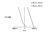
- FIG. 5 is a view showing the relationship between the thickness of the glass member constituting the radiation detection panel 1 and the stress obtained by the analysis when a constant load is applied in the same configuration as the experiment of FIG.
- the combinations of (second ( ⁇ ), third ( ⁇ )) are indicated by solid lines as combinations in which the difference in fracture load is large in FIG. 3, and (second ( ⁇ ), third ( ⁇ )) Combinations are indicated by broken lines.
- the vertical axis indicates the thickness of the glass member
- the horizontal axis indicates the stress applied to the glass member.
- the right side of the horizontal axis is tensile stress
- the left side is compressive stress.
- FIG. 5 in the configuration of the second line ( ⁇ ) and the third line ( ⁇ ) indicated by solid lines, it can be seen that a high tensile stress is applied to the entire glass member. Tensile stress tends to cause breakage for glass members.
- the combination of (second ( ⁇ ) and third ( ⁇ )) indicated by broken lines the tensile stress is entirely shifted in the compression direction.
- the stress state applied to the glass member varies greatly depending on the mechanical relationship around the radiation detection panel.
- mechanical characteristics for protecting the radiation detection panel 1 are also determined by the relationship between the elastic modulus and rigidity of the second component member 61 and the third component member 71 and the rigidity relationship between the housing upper surface 3 a and the base 2. The present inventors have found that changes.
- the radiation detection panel 1 is integrated with a member including a housing upper surface 3 a that is a radiation incident surface of the housing 3, a second component member 61, a third component member 71, and the base 2. ing.
- the rigidity of the structure in which the housing upper surface 3a and the second constituent member 61 arranged in the radiation incident direction are integrated is the third constituent member 71 arranged on the opposite side of the radiation incident direction.
- the rigidity of the structure in which the base 2 is integrated is lower.
- the radiation shielding member 8 is disposed between the base 2 and the third component member 71.
- the radiation shielding member is made of a material containing at least one heavy metal of lead (Pb), barium (Ba), tantalum (Ta), molybdenum (Mo), tungsten (W), or stainless steel. Can be configured.
- the radiation detection panel 1 can be protected from impact and deformation due to external force if the structural relationship (mechanical relationship) of the members around the radiation detection panel 1 is satisfied. That is, according to this embodiment, since the structure which can reduce the load to glass compared with the past can be taken, the weight reduction and thickness reduction of the radiography apparatus 100 are attained.
- FIG. 6 is a cross-sectional view illustrating a configuration example of the radiation imaging apparatus 100 according to the third embodiment.
- the radiation detection panel 1 is supported by the base 2, and the control board 5 that performs readout control of the radiation detection panel 1 and processing of electrical output is the flexible circuit board 4. Is connected to the radiation detection panel 1.
- the radiation detection panel 1 may have a so-called front-surface incident configuration or a back-surface incident configuration.
- the inside of the radiation imaging apparatus 100 has the following configuration as in the first embodiment and the second embodiment in order to protect the radiation detection panel 1. From the order of the radiation incident direction, the housing upper surface 3a which is the radiation incident surface of the housing, the second component member 6, the radiation detection panel 1, the third component member 7, the radiation shielding member 8, and the base 2 It is composed in order.
- the elastic modulus of the second structural member 6 and the third structural member 7 is lower than that of the housing upper surface 3 a, the radiation detection panel 1, and the base 2.
- the rigidity of the second component member 6 is equal to the rigidity of the third component member 7 or lower than the rigidity of the third component member 7.
- the elastic modulus of the second component member 6 is equal to or lower than the elastic modulus of the third component member 7.
- the third component member 7 is made of a material having an elastic modulus equal to that of the second component member 6 or higher than that of the second component member 6. That is, the elastic modulus of the third component member 7 is equal to or greater than the elastic modulus of the second component member 6 (the elastic modulus of the third component member ⁇ the elastic modulus of the second component member 6).
- the elastic modulus of the second component member 6 is equal to or lower than the elastic modulus of the third component member 7, and the second component member 6 is connected to the third component member 7. It is easy to deform compared. Alternatively, the second component member 6 is easily deformed in the same manner as the third component member 7. Therefore, the local deformation of the housing upper surface 3a and the like with respect to the load applied from the outside is absorbed by the deformation of the second component member 6, thereby preventing the influence of the local deformation from reaching the radiation detection panel 1. The radiation detection panel 1 can be protected.
- the plate thickness of the second component member 6 is equal to the plate thickness of the third component member 7, or the third component member 7 is thicker than the plate thickness.
- the elastic modulus of the second component member 6 is equal to or lower than the elastic modulus of the third component member 7.
- the 2nd component member 6 and the 3rd component member 7 are comprised with the shock absorbing material.
- an elastic material such as rubber, foam, elastomer, or gel can be used.
- an elastic material such as rubber, foam, elastomer, or gel can be used as in the second component member 6. If there is, it is not limited to it.
- CFRP or the like can be used for the upper surface 3a of the housing from the relationship between sufficient rigidity and radiation transmittance.
- the base 2 since the base 2 needs to have sufficient rigidity, it is a structure having high rigidity such as fiber reinforced plastic such as CFRP, magnesium alloy, and aluminum alloy, and has higher rigidity than the upper surface 3a of the housing.
- these members may be bonded and integrated as in the second embodiment, or may not be bonded as in the first embodiment.
- attached the one part structural member mentioned above may be sufficient.
- the base 2 is fastened to the housing 3 by fastening members (for example, bolts, screws, pins). Since the housing 3 and the base 2 are integrated, the rigidity of the radiation imaging apparatus 100 can be increased. Since the housing 3 and the base 2 are integrated to increase the rigidity, the rigidity required for other components can be reduced. As a result, the radiation imaging apparatus 100 can be reduced in weight and thickness.
- fastening members for example, bolts, screws, pins
- the radiation detection panel 1 can be protected from impact and deformation due to external force if the structural relationship (mechanical relationship) of the members around the radiation detection panel 1 is satisfied.
- the highly rigid structure does not necessarily need to be the housing upper surface 3a and the base 2.
- the structure which can reduce the load to glass can be taken compared with the past, the weight reduction and thickness reduction of the radiography apparatus 100 are attained.
Landscapes
- Physics & Mathematics (AREA)
- General Physics & Mathematics (AREA)
- Spectroscopy & Molecular Physics (AREA)
- High Energy & Nuclear Physics (AREA)
- Health & Medical Sciences (AREA)
- Life Sciences & Earth Sciences (AREA)
- Molecular Biology (AREA)
- Engineering & Computer Science (AREA)
- General Engineering & Computer Science (AREA)
- Measurement Of Radiation (AREA)
- Apparatus For Radiation Diagnosis (AREA)
Priority Applications (2)
| Application Number | Priority Date | Filing Date | Title |
|---|---|---|---|
| CN201480040904.5A CN105393143A (zh) | 2013-07-24 | 2014-07-15 | 放射线成像装置 |
| US14/959,554 US9976897B2 (en) | 2013-07-24 | 2015-12-04 | Radiation imaging apparatus |
Applications Claiming Priority (2)
| Application Number | Priority Date | Filing Date | Title |
|---|---|---|---|
| JP2013153829A JP2015025682A (ja) | 2013-07-24 | 2013-07-24 | 放射線撮影装置 |
| JP2013-153829 | 2013-07-24 |
Related Child Applications (1)
| Application Number | Title | Priority Date | Filing Date |
|---|---|---|---|
| US14/959,554 Continuation US9976897B2 (en) | 2013-07-24 | 2015-12-04 | Radiation imaging apparatus |
Publications (1)
| Publication Number | Publication Date |
|---|---|
| WO2015011894A1 true WO2015011894A1 (ja) | 2015-01-29 |
Family
ID=52392959
Family Applications (1)
| Application Number | Title | Priority Date | Filing Date |
|---|---|---|---|
| PCT/JP2014/003731 Ceased WO2015011894A1 (ja) | 2013-07-24 | 2014-07-15 | 放射線撮影装置 |
Country Status (4)
| Country | Link |
|---|---|
| US (1) | US9976897B2 (enExample) |
| JP (1) | JP2015025682A (enExample) |
| CN (1) | CN105393143A (enExample) |
| WO (1) | WO2015011894A1 (enExample) |
Families Citing this family (3)
| Publication number | Priority date | Publication date | Assignee | Title |
|---|---|---|---|---|
| JP6606388B2 (ja) | 2015-09-29 | 2019-11-13 | キヤノン株式会社 | 放射線撮影装置および放射線撮影システム |
| JP7054356B2 (ja) | 2018-03-20 | 2022-04-13 | キヤノン株式会社 | 放射線撮影装置 |
| JP7540363B2 (ja) * | 2021-02-24 | 2024-08-27 | コニカミノルタ株式会社 | 放射線画像撮影装置 |
Citations (3)
| Publication number | Priority date | Publication date | Assignee | Title |
|---|---|---|---|---|
| JP2008212343A (ja) * | 2007-03-02 | 2008-09-18 | General Electric Co <Ge> | 軽量で頑丈なディジタルx線検出器 |
| JP2009020099A (ja) * | 2007-07-10 | 2009-01-29 | General Electric Co <Ge> | ディジタルx線検出器 |
| JP2013072808A (ja) * | 2011-09-28 | 2013-04-22 | Fujifilm Corp | カセッテ |
Family Cites Families (18)
| Publication number | Priority date | Publication date | Assignee | Title |
|---|---|---|---|---|
| JP3333278B2 (ja) | 1993-07-14 | 2002-10-15 | 富士写真フイルム株式会社 | 放射線画像検出方法および放射線画像検出器 |
| JP3066944B2 (ja) | 1993-12-27 | 2000-07-17 | キヤノン株式会社 | 光電変換装置、その駆動方法及びそれを有するシステム |
| JP3815766B2 (ja) | 1998-01-28 | 2006-08-30 | キヤノン株式会社 | 二次元撮像装置 |
| JP4497663B2 (ja) | 2000-06-09 | 2010-07-07 | キヤノン株式会社 | 放射線画像撮影装置 |
| US20070085015A1 (en) * | 2005-10-14 | 2007-04-19 | Castleberry Donald E | Lightweight and rugged digital x-ray detector |
| US7495226B2 (en) * | 2006-05-26 | 2009-02-24 | Carestream Health, Inc. | Compact and durable encasement for a digital radiography detector |
| JP4208907B2 (ja) | 2006-07-24 | 2009-01-14 | キヤノン株式会社 | 放射線画像撮影装置 |
| CN101501743B (zh) * | 2006-08-11 | 2011-07-06 | 夏普株式会社 | 显示装置和包括该显示装置的电子设备 |
| US20080078940A1 (en) * | 2006-10-03 | 2008-04-03 | General Electric Company | Portable imaging device having shock absorbent assembly |
| US7488946B2 (en) * | 2006-10-03 | 2009-02-10 | General Electric Company | Digital x-ray detectors |
| JP5238652B2 (ja) | 2009-09-11 | 2013-07-17 | 富士フイルム株式会社 | 放射線画像撮影装置 |
| JP5629445B2 (ja) | 2009-09-25 | 2014-11-19 | キヤノン株式会社 | X線画像撮影装置 |
| US9269741B2 (en) * | 2010-09-07 | 2016-02-23 | Konica Minolta Medical & Graphic, Inc. | Production method of radiation image detector and radiation image detector |
| JP2012078664A (ja) | 2010-10-04 | 2012-04-19 | Fujifilm Corp | 放射線画像撮影装置、放射線画像撮影システム及び放射線画像撮影装置の傷修復方法 |
| US20130134319A1 (en) * | 2011-11-30 | 2013-05-30 | General Electric Company | Mechanical shock isolation for a radiographic device |
| JP2014074595A (ja) * | 2012-10-02 | 2014-04-24 | Canon Inc | 放射線撮像装置、放射線撮像システム、及び、放射線撮像装置の製造方法 |
| JP6092568B2 (ja) * | 2012-10-11 | 2017-03-08 | キヤノン株式会社 | 放射線検出装置及び放射線検出システム |
| JP6397208B2 (ja) | 2014-04-09 | 2018-09-26 | キヤノン株式会社 | 放射線画像撮影装置および放射線画像撮影システム |
-
2013
- 2013-07-24 JP JP2013153829A patent/JP2015025682A/ja active Pending
-
2014
- 2014-07-15 WO PCT/JP2014/003731 patent/WO2015011894A1/ja not_active Ceased
- 2014-07-15 CN CN201480040904.5A patent/CN105393143A/zh active Pending
-
2015
- 2015-12-04 US US14/959,554 patent/US9976897B2/en active Active
Patent Citations (3)
| Publication number | Priority date | Publication date | Assignee | Title |
|---|---|---|---|---|
| JP2008212343A (ja) * | 2007-03-02 | 2008-09-18 | General Electric Co <Ge> | 軽量で頑丈なディジタルx線検出器 |
| JP2009020099A (ja) * | 2007-07-10 | 2009-01-29 | General Electric Co <Ge> | ディジタルx線検出器 |
| JP2013072808A (ja) * | 2011-09-28 | 2013-04-22 | Fujifilm Corp | カセッテ |
Also Published As
| Publication number | Publication date |
|---|---|
| JP2015025682A (ja) | 2015-02-05 |
| CN105393143A (zh) | 2016-03-09 |
| US9976897B2 (en) | 2018-05-22 |
| US20160084704A1 (en) | 2016-03-24 |
Similar Documents
| Publication | Publication Date | Title |
|---|---|---|
| US9354333B2 (en) | Radiation detection apparatus and imaging system | |
| US10061042B2 (en) | Radiation imaging apparatus and radiation imaging system | |
| JP6397208B2 (ja) | 放射線画像撮影装置および放射線画像撮影システム | |
| JP4012182B2 (ja) | カセッテ型x線画像撮影装置 | |
| CN102460216B (zh) | 放射线摄像设备 | |
| US10119859B2 (en) | Radiation imaging apparatus having a buffer member in a corner and radiation imaging system | |
| JP5629445B2 (ja) | X線画像撮影装置 | |
| US20160282482A1 (en) | Radiation imaging apparatus and radiation imaging system | |
| WO2014080692A1 (ja) | 可搬型放射線画像撮影装置 | |
| US20240385339A1 (en) | Radiation image photographing apparatus | |
| JP7370950B2 (ja) | 放射線画像撮影装置 | |
| CN105662442B (zh) | 放射线成像系统 | |
| WO2015011894A1 (ja) | 放射線撮影装置 | |
| JP2008129231A (ja) | カセッテ型放射線画像検出器 | |
| JP2015138008A (ja) | 放射線撮影装置、放射線撮影システム | |
| JP6312445B2 (ja) | 放射線撮影装置及び放射線撮影システム | |
| JP6626548B2 (ja) | 放射線画像撮影装置および放射線画像撮影システム | |
| JP6184136B2 (ja) | 放射線検出装置 | |
| JP6824365B2 (ja) | 放射線画像撮影装置および放射線画像撮影システム | |
| JP2011117760A (ja) | 平面型x線検出装置 | |
| JP2022111805A (ja) | 放射線撮影装置 |
Legal Events
| Date | Code | Title | Description |
|---|---|---|---|
| WWE | Wipo information: entry into national phase |
Ref document number: 201480040904.5 Country of ref document: CN |
|
| 121 | Ep: the epo has been informed by wipo that ep was designated in this application |
Ref document number: 14829034 Country of ref document: EP Kind code of ref document: A1 |
|
| NENP | Non-entry into the national phase |
Ref country code: DE |
|
| 122 | Ep: pct application non-entry in european phase |
Ref document number: 14829034 Country of ref document: EP Kind code of ref document: A1 |