WO2015008656A1 - 照明装置、表示装置、及びテレビ受信装置 - Google Patents
照明装置、表示装置、及びテレビ受信装置 Download PDFInfo
- Publication number
- WO2015008656A1 WO2015008656A1 PCT/JP2014/068131 JP2014068131W WO2015008656A1 WO 2015008656 A1 WO2015008656 A1 WO 2015008656A1 JP 2014068131 W JP2014068131 W JP 2014068131W WO 2015008656 A1 WO2015008656 A1 WO 2015008656A1
- Authority
- WO
- WIPO (PCT)
- Prior art keywords
- light
- guide plate
- light guide
- light incident
- protrusion
- Prior art date
- Legal status (The legal status is an assumption and is not a legal conclusion. Google has not performed a legal analysis and makes no representation as to the accuracy of the status listed.)
- Ceased
Links
Images








Classifications
-
- G—PHYSICS
- G02—OPTICS
- G02B—OPTICAL ELEMENTS, SYSTEMS OR APPARATUS
- G02B6/00—Light guides; Structural details of arrangements comprising light guides and other optical elements, e.g. couplings
- G02B6/0001—Light guides; Structural details of arrangements comprising light guides and other optical elements, e.g. couplings specially adapted for lighting devices or systems
- G02B6/0011—Light guides; Structural details of arrangements comprising light guides and other optical elements, e.g. couplings specially adapted for lighting devices or systems the light guides being planar or of plate-like form
- G02B6/0081—Mechanical or electrical aspects of the light guide and light source in the lighting device peculiar to the adaptation to planar light guides, e.g. concerning packaging
- G02B6/0085—Means for removing heat created by the light source from the package
-
- G—PHYSICS
- G02—OPTICS
- G02B—OPTICAL ELEMENTS, SYSTEMS OR APPARATUS
- G02B6/00—Light guides; Structural details of arrangements comprising light guides and other optical elements, e.g. couplings
- G02B6/0001—Light guides; Structural details of arrangements comprising light guides and other optical elements, e.g. couplings specially adapted for lighting devices or systems
- G02B6/0011—Light guides; Structural details of arrangements comprising light guides and other optical elements, e.g. couplings specially adapted for lighting devices or systems the light guides being planar or of plate-like form
- G02B6/0081—Mechanical or electrical aspects of the light guide and light source in the lighting device peculiar to the adaptation to planar light guides, e.g. concerning packaging
- G02B6/0086—Positioning aspects
- G02B6/0088—Positioning aspects of the light guide or other optical sheets in the package
-
- G—PHYSICS
- G02—OPTICS
- G02B—OPTICAL ELEMENTS, SYSTEMS OR APPARATUS
- G02B6/00—Light guides; Structural details of arrangements comprising light guides and other optical elements, e.g. couplings
- G02B6/0001—Light guides; Structural details of arrangements comprising light guides and other optical elements, e.g. couplings specially adapted for lighting devices or systems
- G02B6/0011—Light guides; Structural details of arrangements comprising light guides and other optical elements, e.g. couplings specially adapted for lighting devices or systems the light guides being planar or of plate-like form
- G02B6/0081—Mechanical or electrical aspects of the light guide and light source in the lighting device peculiar to the adaptation to planar light guides, e.g. concerning packaging
- G02B6/0086—Positioning aspects
- G02B6/0091—Positioning aspects of the light source relative to the light guide
Definitions
- the present invention relates to a lighting device, a display device, and a television receiver.
- a liquid crystal display device such as a liquid crystal television requires a backlight device as a separate illumination device because the liquid crystal panel that is the display panel does not emit light.
- Backlight devices in this type of liquid crystal display device are roughly classified into direct type and edge light type depending on the mechanism. In order to realize further thinning of the liquid crystal display device, an edge light type backlight is used. It is preferred to use an apparatus.
- the distance between the light source such as the LED and the light guide plate may change due to thermal expansion of the light guide plate, and the utilization efficiency of the light emitted from the light source may decrease.
- a fixing member for fixing the substrate on which the light source is mounted to the light guide plate is provided, and the distance between the light source and the light guide plate is kept constant by the fixing member, thereby maintaining a good optical design.
- An illumination device having such a configuration is disclosed in Patent Document 1, for example. In this lighting device, the distance between the LED and the light guide plate is kept constant by fitting a positioning boss disposed on the printed circuit board on which the LED is mounted into a hole provided in the light guide plate. ing.
- the positioning boss is a separate member from the printed circuit board on which the light source is mounted. For this reason, a dimensional variation or a manufacturing variation between members may occur between the positioning boss and the printed board. When such a variation occurs, the distance between the LED and the light guide plate cannot be kept constant among the lighting devices, and it becomes difficult to maintain a good optical design.
- An object of the present specification is to provide a technique capable of maintaining a good optical design while reducing dimensional variations of members.
- the technology disclosed in this specification is provided on a light source, at least one end face, a light incident surface on which light from the light source is incident, and one plate surface, and the light from the light source is emitted.
- a light guide plate having a light output surface and an opposite surface provided on a plate surface opposite to the light output surface, and having heat dissipation, the opposite surface on the opposite surface side of the light guide plate
- a heat dissipating member having a bottom surface portion arranged in a shape along the surface, and a rising portion rising from the bottom surface portion toward the light emitting surface side, wherein the bottom surface portion faces at least one end surface of the light guide plate.
- the heat dissipation is provided with a protrusion that protrudes from the bottom surface portion to the light emitting surface side and is locked to the opposite end surface to restrict the distance between the light source and the light incident surface.
- a lighting device including the member.
- the distance between the light source and the light incident surface is regulated by locking the protrusion of the heat radiating member with the end surface of the light guide plate. Even in such a case, the distance between the light source and the light incident surface hardly changes, and good optical characteristics can be maintained. Further, since the protrusion is a part of the existing heat dissipation member, it is not necessary to add a new member to regulate the distance between the light source and the light incident surface, and the member accompanying the addition of the member is not necessary. Dimensional variation and manufacturing variation can be reduced. As described above, in the above-described illumination device, it is possible to maintain a good optical design while reducing the dimensional variation of the members.
- a reflective sheet having light reflectivity is disposed between the opposite surface of the light guide plate and the bottom surface of the heat dissipating member, and the protrusion is engaged with the reflective sheet so that the reflective sheet is
- the movement in the direction orthogonal to the light incident surface may be restricted.
- the reflection sheet is restricted from moving in the direction orthogonal to the light incident surface by the protruding portion, the distance between the light source and the reflection sheet varies even when the reflection sheet is thermally expanded. Can be difficult. Thereby, it can prevent thru
- an end surface adjacent to the light incident surface may be an adjacent end surface, and the adjacent end surface may be provided with a notch that faces the protrusion and can be fitted to the protrusion.
- a specific structure can be provided about the latching aspect of the end surface of a light-guide plate and the protrusion part of a thermal radiation member.
- the notch of the light guide plate may be provided at a position that does not overlap a range of a light distribution of light incident from the light incident surface. According to this configuration, since the light incident from the light incident surface is not blocked by the protrusion fitted into the notch, luminance unevenness occurs on the light emitting surface due to the blocking. Can be prevented.
- the projecting portion may include a pasting portion that is pasted on the light incident surface. According to this, it is possible to realize a configuration in which the distance between the light source and the light incident surface can be regulated by the protruding portion without providing a notch or the like in the light guide plate. For this reason, it is not necessary to process a light-guide plate, and the manufacturing process of an illuminating device can be simplified.
- part affixed with the said affixing part among the said light-incidence surfaces of the said light-guide plate may be made into the position which does not overlap with the light distribution of the light which injects from the said light-incidence surface. According to this configuration, since the light incident from the light incident surface is not blocked by the pasting portion, light incident from the light incident surface is blocked by the light incident from the light incident surface. A reduction in luminance can be prevented.
- an end surface adjacent to the light incident surface may be an adjacent end surface
- the protruding portion may have a contact portion in contact with the adjacent end surface
- the projecting portion may be provided in a form continuous with the rising portion. According to this configuration, the strength of the protruding portion can be increased as compared with the configuration in which the protruding portion protruding from the bottom surface portion is provided apart from the rising portion.
- a urethane member may be attached to the outer peripheral surface of the protruding portion. According to this configuration, when the protruding portion strongly interferes with the end surface of the light guide plate, an impact or the like is absorbed by the urethane member. This can be prevented or suppressed.
- a reflective member having light reflectivity may be attached to the outer peripheral surface of the protruding portion. According to this configuration, since the light directed from the light source or the light guide plate toward the projecting portion is reflected by the projecting portion, the brightness of the light emitted from the light exit surface is reduced due to light leakage. It can be prevented or suppressed.
- a light source substrate on which the light source is mounted on one plate surface may be provided, and the other plate surface of the light source substrate may be attached to the rising portion. Since the protruding portion is provided on the bottom surface portion of the heat radiating member, according to the above configuration, the light source substrate attached to the rising portion of the heat radiating member does not interfere with the protruding portion, and the protruding portion causes a gap between the light source and the light incident surface. Can be effectively regulated.
- the technology disclosed in this specification can also be expressed as a display device including the above-described lighting device and a display panel that performs display using light from the lighting device.
- a display device in which the display panel is a liquid crystal panel using liquid crystal is also new and useful.
- a television receiver provided with the above display device is also new and useful.
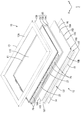
- FIG. 1 is an exploded perspective view showing a schematic configuration of a television receiver according to Embodiment 1.
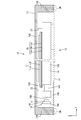
- FIG. Rear view of TV receiver Exploded perspective view showing schematic configuration of liquid crystal display device Sectional drawing of the cross section which cut
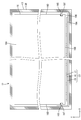
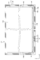
- FIG. 6 is an enlarged plan sectional view of the vicinity of one protrusion.
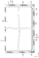
- FIG. 5 is a cross-sectional plan view of the backlight device according to the second embodiment viewed from the light exit surface side of the light guide plate.
- FIG. 9 is an enlarged plan sectional view of the vicinity of one protrusion.
- FIG. 5 is a cross-sectional plan view of the backlight device according to the third embodiment when viewed from the light exit surface side of the light guide plate.
- 12 is an enlarged plan sectional view of the vicinity of one protrusion in FIG. Plane sectional view of the backlight device according to Embodiment 4 viewed from the light exit surface side of the light guide plate
- Embodiment 1 will be described with reference to the drawings.
- a liquid crystal display device an example of a display device 10 is illustrated.
- a part of each drawing shows an X-axis, a Y-axis, and a Z-axis, and each axis direction is drawn in a common direction in each drawing.
- the Y-axis direction coincides with the vertical direction
- the X-axis direction coincides with the horizontal direction.
- the vertical direction is used as a reference for upper and lower descriptions.
- the television receiver TV includes a liquid crystal display device 10, various substrates PWB, MB, and CTB attached to the back side (back side) of the liquid crystal display device 10, and the back side of the liquid crystal display device 10.
- a cover member CV attached to cover each main substrate PWB, MB, CTB and a stand ST are provided.
- the television receiver TV is held in a state in which the display surface of the liquid crystal display device 10 is along the vertical direction (Y-axis direction) by the stand ST.
- the liquid crystal display device 10 has a horizontally long rectangular shape (rectangular shape, longitudinal shape) as a whole, and includes a liquid crystal panel 11 that is a display panel and a backlight device 12 that is an external light source. These are configured to be integrally held by the frame 13 and the chassis 14 which are appearance members constituting the appearance of the liquid crystal display device 10.
- a pair of stand attachment members STC extending along the Y-axis direction are attached to two positions spaced apart in the X-axis direction on the back surface of the chassis 14 constituting the back side appearance of the liquid crystal display device 10. It has been.
- These stand attachment members STC have a substantially channel shape with a cross-sectional shape opened on the surface on the chassis 14 side, and a pair of support columns STB in the stand ST are inserted into a space held between the stand 14 and the chassis 14. It has become.
- the wiring member (electric wire etc.) connected to the LED board 18 which the backlight apparatus 12 has is passed through the space in the stand attachment member STC.
- the stand ST includes a pedestal portion STA that is parallel to the X-axis direction and the Z-axis direction, and a pair of column portions STB that rise from the pedestal portion STA along the Y-axis direction.
- the cover member CV is made of synthetic resin, and covers a part of the back surface of the chassis 14, specifically about the lower half of FIG. 2, while traversing the pair of stand mounting members STC in the X-axis direction. It is attached in the form. Between the cover member CV and the chassis 14, there is a component storage space that can store components such as various substrates PWB, MB, and CTB described below.
- the various substrates PWB, MB, and CTB include a power supply substrate PWB, a main substrate MB, and a control substrate CTB.
- the power supply substrate PWB can be said to be a power supply source of the liquid crystal display device 10 and supplies driving power to the other substrates MB and CTB and the LED (an example of a light source) 17 included in the backlight device 12. It is possible. Therefore, it can be said that the power supply substrate PWB also serves as an LED drive substrate for driving the LEDs 17.
- the main board MB includes at least a tuner unit capable of receiving a television signal and an image processing unit (not shown) for processing the received television signal, and controls the processed image signal as follows. Output to the substrate CTB is possible.
- the main board MB receives an image signal from the image reproduction device when the liquid crystal display device 10 is connected to an external image reproduction device (not shown). It can be processed and output to the control board CTB.
- the control board CTB has a function of converting an image signal input from the main board into a liquid crystal driving signal and supplying the converted liquid crystal driving signal to the liquid crystal panel 11.
- the liquid crystal display device 10 includes a main component in a space held between a frame 13 constituting the front side appearance and a chassis 14 constituting the back side appearance. It is supposed to be housed in The main components housed in the frame 13 and the chassis 14 include at least the liquid crystal panel 11, the optical member 15, the light guide plate 16, and the LED unit LU. Among these, the liquid crystal panel 11, the optical member 15, and the light guide plate 16 are held in a state of being sandwiched between the front frame 13 and the back chassis 14 in a state where they are stacked on each other.
- the backlight device 12 includes an optical member 15, a light guide plate 16, an LED unit LU, and a chassis 14, and is configured by removing the liquid crystal panel 11 and the frame 13 from the liquid crystal display device 10 described above.
- the LED unit LU is arranged so as to face the end surface of one long side of the light guide plate 16.
- the liquid crystal panel 11 has a horizontally long rectangular shape (rectangular shape, rectangular shape) in a plan view, and a pair of glass substrates 11A and 11B (see FIG. 4) having excellent translucency. ) Are bonded together with a predetermined gap therebetween, and liquid crystal is sealed between the substrates 11A and 11B.
- One substrate (array substrate) 11B is provided with a switching element (for example, TFT) connected to the source wiring and the gate wiring orthogonal to each other, a pixel electrode connected to the switching element, an alignment film, and the like.
- a switching element for example, TFT
- the other substrate (CF substrate) 11A includes a color filter, a counter electrode, an alignment film, and the like in which colored portions such as R (red), G (green), and B (blue) are arranged in a predetermined arrangement. Is provided.
- the liquid crystal panel 11 is placed on the front side of the optical member 15 to be described later, and the back surface (the outer surface of the polarizing plate on the back side) is in close contact with the optical member 15 with almost no gap. This prevents dust and the like from entering between the liquid crystal panel 11 and the optical member 15.
- the display surface 11C of the liquid crystal panel 11 includes a display area on the center side of the screen where images can be displayed, and a non-display area having a frame shape (frame shape) surrounding the display area on the outer peripheral edge side of the screen.
- the liquid crystal panel 11 is connected to a control board (not shown) via a driver component for driving liquid crystal and a flexible board (not shown), and an image is displayed on the display area of the display surface 11C based on a signal input from the control board. It is displayed.
- a polarizing plate (not shown) is disposed outside each of the substrates 11A and 11B.
- the frame 13 is made of a metal such as aluminum, for example, and has higher mechanical strength (rigidity) and thermal conductivity than a case where it is made of a synthetic resin. As shown in FIG. 3, the frame 13 has a horizontally long frame shape as a whole so as to surround a display area on the display surface 11 ⁇ / b> C of the liquid crystal panel 11.
- the frame 13 includes a panel pressing portion 13A that is parallel to the display surface 11C of the liquid crystal panel 11 and presses the liquid crystal panel 11 from the front side, and a side wall portion 13B that protrudes from the outer peripheral side portion of the panel pressing portion 13A toward the back side.
- the cross-sectional shape is substantially L-shaped.
- the panel pressing portion 13A has a horizontally long frame shape following the outer peripheral side portion of the liquid crystal panel 11 and can press the outer peripheral side portion of the liquid crystal panel 11 from the front side over almost the entire circumference.
- the panel pressing portion 13 ⁇ / b> A includes the optical member 15 and the outer peripheral portion of the light guide plate 16 that are arranged on the outer side in the radial direction than the outer peripheral portion of the liquid crystal panel 11, and the LED unit LU. Has a width that can be covered from the front side.
- the outer surface facing the front side of the panel pressing portion 13A (the surface opposite to the surface facing the liquid crystal panel 11) is exposed to the outside on the front side of the liquid crystal display device 10 like the display surface 11C of the liquid crystal panel 11.
- the front surface of the liquid crystal display device 10 is configured together with the display surface 11 ⁇ / b> C of the panel 11.
- the inner edge portion of the panel pressing portion 13 ⁇ / b> A has a protruding shape that protrudes toward the back side, that is, the liquid crystal panel 11 side.
- a cushioning material 24 is attached to the projecting front end surface of the projection, and the liquid crystal panel 11 can be pressed from the front side via the cushioning material 24.
- the cushioning material 24 has a frame shape arranged over the entire circumference at the inner peripheral edge of the panel pressing portion 13A.
- the side wall portion 13B has a substantially rectangular tube shape protruding from the outer peripheral side portion (specifically, the outer peripheral end portion) of the panel pressing portion 13A toward the back side.
- the side wall portion 13B can surround the liquid crystal panel 11, the optical member 15, the light guide plate 16, and the LED unit LU accommodated therein, and can also surround the back side chassis 14 over almost the entire periphery.
- the side wall portion 13 ⁇ / b> B has an outer surface along the circumferential direction of the liquid crystal display device 10 exposed to the outside in the circumferential direction of the liquid crystal display device 10, and constitutes a top surface, a bottom surface, and both side surfaces of the liquid crystal display device 10.
- the side wall 13B is formed with a screw groove 13B1 that opens toward the back side and can fasten the screw member SM.
- Abutting ribs 23 that support the light guide plate 16 from the front side are integrally formed at a position inward of the side wall portion 13B in the panel pressing portion 13A.
- the abutment ribs 23 project from the inner surface of the panel pressing portion 13A toward the back side (light guide plate 16 side) along the Z-axis direction, and extend along each side of the panel pressing portion 13A. It has a shape.
- the contact ribs 23 are provided on the respective sides of the panel pressing portion 13A, and each has a length dimension over the entire length of each side. Therefore, the abutment rib 23 can be supported from the front side (display surface 11C side) with the light guide plate 16 sandwiched between the chassis 14 and has a light guide plate support function.
- the light guide plate 16 is pressed from the front side by the contact rib 23 whose end side portion forms a frame shape over the entire circumference.
- the chassis 14 is made of a metal such as aluminum like the frame 13, and has higher mechanical strength (rigidity) and thermal conductivity than a case where it is made of a synthetic resin. As shown in FIG. 3, the chassis 14 has a horizontally long flat plate shape as in the light guide plate 16 to be described later so as to cover the light guide plate 16 and the LED unit LU over almost the entire region from the back side. The surface of the chassis 14 is opposed to an opposite surface 16C of the light guide plate 16 described later and the LED unit LU. On the other hand, the back surface of the chassis 14 is exposed outside the back side of the liquid crystal display device 10 and constitutes the back surface of the liquid crystal display device 10.
- a plurality of screw insertion holes (not shown) through which the screw members SM are inserted are provided at the outer peripheral end of the chassis 14.
- the chassis 14 is brought into contact with the side wall portion so that the screw insertion hole and the screw groove 13B1 provided in the side wall portion of the frame 13 overlap with each other, and the screw member SM is tightened, whereby the frame 13 and the chassis 14 are connected. They are assembled in a fixed state.
- the frame 13 and the chassis 14 are stacked on each other while accommodating the LED unit LU at one end in the short side direction (one long side end). 11.
- the optical member 15 and the light guide plate 16 are accommodated so as to be sandwiched between the front side and the back side.
- the optical member 15 has a horizontally long rectangular shape as viewed from the same plane as the liquid crystal panel 11, and its size (short side dimension and long side dimension) is substantially the same as the liquid crystal panel 11. It is said.
- the optical member 15 is placed so as to be laminated on the front side (light emitting side) of the light guide plate 16 described later, and is disposed in a state of being sandwiched between the liquid crystal panel 11 and the light guide plate 16 described above.
- the optical member 18 is formed by laminating three sheet-like members of a diffusion sheet 15A, a lens sheet 15B, and a reflective polarizing sheet 15C in this order from the light guide plate 20 side (back side). Each of the three sheets has substantially the same size when viewed in a plane.
- the light guide plate 16 is made of a synthetic resin material (for example, acrylic resin such as PMMA or polycarbonate) having a refractive index sufficiently higher than that of air and substantially transparent (excellent translucency). As shown in FIG. 3, the light guide plate 16 has a horizontally long rectangular shape when viewed in a plan view, as in the liquid crystal panel 11 and the optical member 15, and has a plate shape that is thicker than the optical member 15. The long side direction on the surface coincides with the X-axis direction, the short side direction coincides with the Y-axis direction, and the plate thickness direction orthogonal to the main surface coincides with the Z-axis direction.
- a synthetic resin material for example, acrylic resin such as PMMA or polycarbonate
- the light guide plate 16 is laminated on the back side of the optical member 15 and is disposed so as to be sandwiched between the optical member 15 and the chassis 14. As shown in FIG. 4, the light guide plate 16 has at least a short side dimension larger than each short side dimension of the liquid crystal panel 11 and the optical member 15, and both end portions in the short side direction (long side direction). Are arranged so as to protrude outward from both ends of the liquid crystal panel 11 and the optical member 15 (so as to be non-overlapping in a plan view).
- One end surface on the long side of the light guide plate 16 is a light incident surface 16B on which light emitted from the LED 17 described later is incident.
- the surface facing the front side is a light emitting surface 16 ⁇ / b> A that emits internal light toward the optical member 15 and the liquid crystal panel 11.
- the opposite surface 16C opposite to the light emitting surface 16A is provided in a covering form.
- the alignment direction with the LEDs 17 coincides with the Y-axis direction
- the alignment direction with the optical member 15 and the reflection sheet 20 coincides with the Z-axis direction.
- the light guide plate 16 has a function of introducing the light emitted from the LED unit LU from the light incident surface 16B and raising the light toward the optical member 15 while propagating the light inside to emit the light from the light emitting surface 16A. Have.
- Both end surfaces on the short side of the light guide plate 16 are adjacent end surfaces 16D adjacent to the light incident surface 16B (see FIGS. 3 and 5).
- Each adjacent end face 16 ⁇ / b> D in the light guide plate 16 is provided with a notch 16 ⁇ / b> S having a concave shape toward the center side of the light guide plate 16.
- each notch 16S has the light guide plate 16 in the thickness direction (Z-axis direction) so as to have a rectangular shape in plan view at a position near the light incident surface 16B in each adjacent end face 16D. It is provided in a penetrating form.
- the positions of the notches 16S coincide with each other in the short side direction (Y-axis direction) of the light guide plate 16.
- the reflection sheet 20 has a rectangular sheet shape, is made of synthetic resin, and has a white surface with excellent light reflectivity.
- the reflection sheet 20 is arranged in such a manner that the long side direction thereof coincides with the X-axis direction, the short side direction thereof coincides with the Y-axis direction, and is slightly separated from the chassis 14.
- the reflection sheet 20 has a reflection surface on the front side, and this reflection surface is in contact with the opposite surface 16C of the light guide plate 16, and reflects light leaked from the LED unit LU or the light guide plate 16 to the reflection surface 16C side. It is possible to make it.
- the short side dimension of the reflection sheet 20 is substantially equal to the short side dimension of the light guide plate 16.
- the LED 17 constituting the LED unit LU has a configuration in which an LED chip (not shown) is sealed with a resin material on a substrate portion fixed to the LED substrate 18.
- the LED chip mounted on the substrate unit has one main emission wavelength, and specifically, one that emits blue light in a single color is used.
- the resin material that seals the LED chip is dispersed and blended with a phosphor that emits a predetermined color when excited by the blue light emitted from the LED chip, and generally emits white light as a whole. It is said.
- the LED 17 is a so-called top surface light emitting type in which a surface opposite to the mounting surface with respect to the LED substrate 18 is a main light emitting surface. Each LED 17 is arranged such that its light emitting surface faces the light incident surface 16B of the light guide plate 16.
- the LED substrate 18 constituting the LED unit LU has an elongated plate shape extending along the long side direction (X-axis direction) of the light guide plate 16, and its plate surface Are accommodated in the frame 13 and the chassis 14 in a posture parallel to the X-axis direction and the Z-axis direction, that is, a posture parallel to the light incident surface 16B of the light guide plate 16.
- the LED substrate 18 has a dimension in the long side direction (X-axis direction) slightly smaller than a dimension in the long side direction of the light guide plate 16 (see FIG. 6).
- the LED 17 having the above-described configuration is surface-mounted on the inner surface, that is, the plate surface facing the light guide plate 16 side of the LED substrate 18, and this is the mounting surface.
- a plurality of LEDs 17 are arranged in a line (linearly) in parallel along the length direction (X-axis direction) with a predetermined interval. That is, it can be said that a plurality of LEDs 17 are intermittently arranged in parallel along the long side direction at one end portion on the long side of the backlight device 12.
- the interval between the LEDs 17 adjacent to each other in the X-axis direction, that is, the arrangement pitch of the LEDs 17 is substantially equal.
- the arrangement direction of the LEDs 17 coincides with the long side direction (X-axis direction) of the LED substrate 18.
- a wiring pattern (not shown) made of a metal film (such as a copper foil) that extends along the X-axis direction and connects adjacent LEDs 17 across the LED 17 group in series.
- the terminal portions formed at both ends of the wiring pattern are connected to the power supply substrate PWB via wiring members such as connectors and electric wires so that driving power is supplied to each LED 17. It has become.
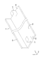
- the heat dissipating member 19 constituting the LED unit LU is made of a metal having excellent thermal conductivity (excellent heat dissipation) such as aluminum, for example, and as shown in FIG.
- the bottom surface portion 19B is in surface contact with the plate surface of the chassis 14 and has a bent shape that is substantially L-shaped in cross-section.
- the rising portion 19A constituting the heat radiating member 19 rises perpendicularly (along the Z-axis direction) to the bottom surface portion 19B from the outer end portion of the bottom surface portion 19B described below toward the front side.
- the rising portion 19A has a plate shape parallel to the plate surface of the LED substrate 18 and the light incident surface 16B of the light guide plate 16, and its long side direction is the X-axis direction, and the short side direction is the Z-axis direction. The direction coincides with the Y-axis direction.
- the LED substrate 18 is attached to the inner plate surface of the rising portion 19A, that is, the plate surface facing the light guide plate 16 side.
- the rising portion 19 ⁇ / b> A has a long side dimension larger than the long side dimension of the light guide plate 16, and a short side dimension larger than the short side dimensions of the light guide plate 16 and the LED substrate 18.
- the bottom surface portion 19 ⁇ / b> B constituting the heat radiating member 19 has a plate shape parallel to the plate surface of the chassis 14.
- the long side direction is the X-axis direction and the short side direction is the Y-axis direction.
- the thickness direction coincides with the Z-axis direction.
- the bottom surface portion 19B extends from the rear end portion (the end portion on the chassis 14 side) of the rising portion 19A so as to protrude inward along the Y-axis direction, that is, toward the center side of the light guide plate 16. Most of them are located on the back side of the light guide plate 16 and on the back side of the reflection sheet 20.
- the bottom surface portion 19 ⁇ / b> B is arranged in such a manner as to be sandwiched (intervened) between the reflection sheet 20 and the chassis 14.
- the bottom surface portion 19 ⁇ / b> B has a long side dimension equivalent to that of the rising portion 19 ⁇ / b> A and is larger than the long side dimension of the light guide plate 16.
- the back plate surface that is, the plate surface facing the chassis 14 side, is in surface contact with the chassis 14 in its entire region. Thereby, the heat transmitted from the LED 17 to the heat radiating member 19 is effectively radiated from the bottom surface portion 19B to the chassis 14 side.
- each part 19T is provided.
- Each protruding portion 19T protrudes in a block shape perpendicularly to the bottom surface portion 19B (along the Z-axis direction) so as to be symmetrical with respect to the light guide plate 16 (see FIG. 8 and the like).
- Each projection 19T is housed in each notch 16S in a state where there is almost no gap between each protrusion 19T and the side surface of each notch 16S in the plan view shown in FIG.
- each protrusion 19T and each notch 16S are fitted, and the light guide plate 16 and the heat radiating member 19 are locked via the protrusion 19T.
- the protrusions 19T and the notches 16S are fitted to each other, so that the space between the protrusions 19T and the side surfaces of the notches 16S is in the plate surface direction (XY plane direction) of the light guide plate 16. ),
- the light guide plate 16 is positioned in the plate surface direction. Thereby, the distance between LED17 and the light-incidence surface 16B of the light-guide plate 16 is controlled.
- the light incident surface 16B of the light guide plate 16 expands in a direction (Y-axis direction) orthogonal to the light incident surface 16B due to heat or the like. Even in this case, the protrusion 19T moves following the expansion of the light incident surface 16B. Accordingly, the LED 17 supported by the heat dissipation member 19 via the heat dissipation member 19 and the LED substrate 18 also moves following the expansion of the light incident surface 16B. As a result, even when the light guide plate 16 undergoes thermal expansion or the like, the distance between the LED 17 and the light incident surface 16B is kept constant, so that a good optical design can be maintained.
- the distance between the LED 17 and the light incident surface 16B can be kept constant. There is no need to distribute. For this reason, compared with the case where another member such as a spacer member is provided, it is possible to reduce dimensional variations and manufacturing variations between the members, and to keep the distance between the LED 17 and the light incident surface 16B constant with high accuracy. be able to.
- the reflection sheet 20 side cutout (not shown) having the same shape and size as each cutout 16S is provided at a position overlapping the cutout 16S provided on the light guide plate 16 in the reflection sheet 20 in plan view. Is provided.
- the protrusion 19T is also fitted to the notch 16S of the light guide plate 16 and the notch 16S of the light guide plate 16, and the reflection sheet 20 is similarly fitted to the sheet surface direction (X ⁇ ). It is positioned with respect to the Y plane direction).
- the distance between the LED 17 and the reflection sheet 20 is also kept constant, and the light leaked to the reflection sheet 20 side can be reflected well, so that a decrease in luminance can be prevented or suppressed.
- light leakage and the like can be prevented or suppressed.
- each notch 16S in the light guide plate 16 is provided at a position that does not overlap with the light distribution of the light from the LED 17 incident from the light incident surface 16B (see the dashed line in FIG. 7). It has been. For this reason, it is avoided that the light from the LED 17 is blocked by the protruding portion 19T of the heat radiating member 19 fitted to each notch 16S, and the light is emitted from the light emitting surface 16A due to the blocking. It is prevented or suppressed that brightness unevenness occurs in the light.
- the protrusion 19T of the heat radiating member 19 is fitted with the notch 16S of the light guide plate 16 as described above.
- the light guide plate 16 can be positioned in the plate surface direction (XY plane direction), workability in the manufacturing process can be improved.
- another member such as a spacer member as described above, the manufacturing process can be simplified as compared with the case where the other member is arranged.
- each protrusion 19T of the heat radiating member 19 is engaged with each adjacent end surface 16D of the light guide plate 16 and the protrusion 19T, so that the LED 17 and the LED 17 are guided. Since the distance between the light incident surface 16B of the light plate 16 is regulated, the distance between the LED 17 and the light incident surface 16B is less likely to fluctuate even when the light guide plate 16 undergoes thermal expansion or the like. Optical characteristics can be maintained. Further, since the protruding portion 19T is a part of the existing heat radiating member 19, there is no need to add a new member in order to regulate the distance between the LED 17 and the light incident surface 16B. The accompanying dimensional variations and manufacturing variations of the members can be reduced. As described above, in the backlight device 12 of the present embodiment, it is possible to maintain a good optical design while reducing variations in the dimensions of members.
- the notch 16S of the light guide plate 16 is provided at a position that does not overlap the range of the light distribution of the light incident from the light incident surface 16B.
- the light incident from the light incident surface 16B is not blocked by the protruding portion 16T fitted to the notch 16S, and thus uneven brightness occurs on the light emitting surface 16A due to the blocking. This can be prevented.
- the light source substrate on which the LED is mounted is provided on the mounting surface which is one plate surface, and the other plate surface of the LED substrate is attached to the rising portion of the heat dissipation member.
- the projecting portion 16T is provided on the bottom surface portion 19B of the heat radiating member 19, the LED substrate 18 attached to the rising portion 19A of the heat radiating member 19 interferes with the projecting portion 19T.
- the distance between the LED 17 and the light incident surface 16B can be effectively regulated by the protrusion 19T.
- the heat radiating member 19 is provided with the protrusion 19T, the surface area of the heat radiating member 19 is increased compared to the case where the protrusion 19T is not provided. It can be further enhanced.
- the manufacturing process of the backlight device it is very difficult to process the front and back plate surfaces of the light guide plate, but the end surfaces of the light guide plate are easy to process.
- the notch 16S is provided in the end surface of the light guide plate 16, the manufacturing process can be simplified as compared with the case where recesses and the like are provided in the front and back plate surfaces of the light guide plate 16.
- the notch 16S is provided in a part of the light incident surface 16B, there is a possibility that loss of light incident on the light incident surface 16B is generated by the notch 16S.
- the notch 16S is provided in the adjacent end face 16D adjacent to the light incident surface 16B, so that it is possible to prevent such light loss from occurring.
- a urethane member (not shown) is attached to the outer peripheral surface of each protrusion 19T.
- an impact or the like is absorbed by the urethane member, so that the protrusion 19T is notched 16S of the light guide plate 16. It is possible to prevent or suppress the cutout 16S from being damaged due to the interference with.
- the space between the projecting portion 19T and the notch 16S is filled with the urethane member, even when there is a dimensional variation between the projecting portions 19T, the influence of such a dimensional variation can be reduced.
- ⁇ Modification 2 of Embodiment 1> A second modification of the first embodiment will be described.
- a reflecting member (not shown) having light reflectivity is attached to the outer peripheral surface of each protrusion 19T.
- light directed from the LED 17 or the light guide plate 16 toward the protruding portion 19T is reflected by the protruding portion 19T, and thus is emitted from the light emitting surface 16A due to light leakage. It is possible to prevent or suppress a decrease in the brightness of the light, and to improve the light utilization efficiency.
- various members can be attached to the protruding portion 19T, and a high degree of freedom in design can be ensured.
- each protrusion 119T has a pasting part 119T1 and an abutting part 119T2, and is substantially L-shaped in plan view.
- the affixing portion 119T1 is provided so as to face the end in the long side direction (X-axis direction) of the light incident surface 116B, and is attached to a portion facing the light incident surface 116B via the adhesive tape 130. It is attached. Thereby, the protrusion 119T is locked to the light incident surface 116B which is one end surface of the light guide plate 116, and the distance between the LED 117 and the light incident surface 116B is kept constant.
- the portion of the light incident surface 116B that is attached to the attaching portion 119T1 via the adhesive tape 130 is the light distribution of light from the LED 117 that is incident from the light incident surface 116B. (Refer to the alternate long and short dash line shown in FIG. 10).
- the contact portion 119T2 in each protrusion 119T is continuous with the pasting portion 119T1, and contacts the position near the light incident surface 116B among the adjacent end surfaces 116D in the light guide plate 116. And is provided along the adjacent end face 116D. As described above, the adjacent end surface 116D of the light guide plate 116 contacts the contact portion 119T2 of the protruding portion 119T, so that the light guide plate 116 can be positioned with respect to the direction orthogonal to the adjacent end surface 116D (Y-axis direction).
- the protruding portion 119T since the protruding portion 119T includes the attaching portion 119T1 that is attached to the light incident surface 116B, the protruding portion 119T is provided without providing the notch 116S or the like in the light guide plate 116. Thus, it is possible to realize a configuration capable of regulating the distance between the LED 117 and the light incident surface 116B. Therefore, it is not necessary to process the light guide plate 116, and the manufacturing process of the backlight device 112 can be simplified.
- the affixing part 119T1 is affixed at a position that does not overlap with the light distribution of the light from the LED 117 incident from the light incident surface 116B, the light incident from the light incident surface 116B is transmitted by the affixing part 119T1. There is no obstruction. For this reason, it can prevent that the brightness
- Embodiment 3 will be described with reference to the drawings.
- the shape of the protruding portion 219T provided on the heat dissipation member 219 is different from that of the first embodiment. Since the other configuration is the same as that of the first embodiment, the description of the structure, operation, and effect is omitted.
- FIGS. 12 and 13 the part obtained by adding the numeral 200 to the reference numerals in FIGS. 6 and 7 is the same as the part described in the first embodiment.
- the protrusions 219 ⁇ / b> T are formed from the bottom surface portion 219 ⁇ / b> B on both sides in the long side direction (X-axis direction) of the bottom surface portion 219 ⁇ / b> B of the heat dissipation member 219. It protrudes to the front side and is configured to be continuous with the rising portion 219A.
- each protruding portion 219T is provided on each of both end sides in the long side direction (X-axis direction) of the rising portion 219A.
- Each protrusion 219T has a part of the surface directed toward the light incident surface 216B facing the both ends of the light incident surface 216B in the long side direction. Then, the opposite portion of the protruding portion 219T is attached to the light incident surface 216B via the adhesive tape 230 as in the second embodiment. Thereby, the protrusion 219T is locked to the light incident surface 216B which is one end surface of the light guide plate 216, and the distance between the LED 217 and the light incident surface 216B is kept constant.
- the protruding portion 219T is connected to the rising portion 219A, so that the protruding portion 219T protruding from the bottom surface portion 219B is provided apart from the rising portion 219A.
- strength of the protrusion part 219T can be raised.
- the distance between the LED 217 and the light incident surface 216B can be effectively regulated by the protrusion 219T.
- Embodiment 4 will be described with reference to the drawings.
- the fourth embodiment is different from the first embodiment in the arrangement of the LED units LU and the like. Since the other configuration is the same as that of the first embodiment, the description of the structure, operation, and effect is omitted.
- FIG. 14 the part obtained by adding the numeral 300 to the reference sign in FIG. 6 is the same as the part described in the first embodiment.
- each unit LU is arranged.
- Each LED unit LU has the same configuration as that in the first embodiment, and the arrangement, configuration, and the like of each protrusion 319T provided on each heat radiation member 319 are also the same as those in the first embodiment.
- the distance between each light incident surface 316B and the LED 317 can be regulated by each protrusion 319T. It is possible to maintain a good optical design while reducing dimensional variations of members.
- the configuration of the heat dissipating member including the bottom surface portion and the rising portion can be changed as appropriate.
- the configuration of the protrusions can be changed as appropriate.
- LED substrate 19, 119, 219, 319 ...
- Heat dissipation member 19T, 119T, 219T 319T: Protruding part
- 20 Reflecting sheet, 119T1 ... Pasting part, 119T2 ... Abutting part 130, 230 ... adhesive tape
Landscapes
- Physics & Mathematics (AREA)
- General Physics & Mathematics (AREA)
- Optics & Photonics (AREA)
- Planar Illumination Modules (AREA)
- Liquid Crystal (AREA)
Abstract
Description
しかしながら、上記特許文献1の照明装置において位置決めボスは、光源が実装されるプリント基板とは別部材とされる。このため、位置決めボスとプリント基板との間に、部材間の寸法ばらつきや製造ばらつき等が発生することがある。このようなばらつきが発生すると、各照明装置の間でLEDと導光板との間の距離を一定に保つことができず、良好な光学設計を保つことが困難となる。
本明細書で開示される技術は、光源と、少なくとも一つの端面に設けられ、前記光源からの光が入射される光入射面と、一方の板面に設けられ、前記光源からの光が出射される光出射面と、該光出射面とは反対側の板面に設けられた反対面と、を有する導光板と、放熱性を有し、前記導光板の前記反対面側において該反対面に沿った形で配された底面部と、該底面部から前記光出射面側に立ち上がる立ち上がり部と、を有する放熱部材であって、前記底面部に、前記導光板の少なくとも一つの端面と対向する形で前記底面部から前記光出射面側に突出するとともに前記対向する前記端面に係止されることで前記光源と前記光入射面との間の距離を規制する突出部が設けられた放熱部材と、を備える照明装置に関する。
この構成によると、突出部によって反射シートが光入射面と直交する方向に移動することが規制されるので、反射シートが熱膨張した場合であっても光源と反射シートとの間の距離が変動し難いものとすることができる。これにより、反射シートの機能が低下することを防止ないし抑制することができ、光出射面から出射される光の輝度が低下することを防止ないし抑制することができる。
これによると、導光板の端面と放熱部材の突出部との係止態様について具体的な構成を提供することができる。
この構成によると、光入射面から入射される光が切り欠きと嵌合された突出部によって遮られることがないので、当該遮られることに起因して光出射面において輝度ムラが発生することを防止することができる。
これによると、導光板に切り欠き等を設けることなく、突出部によって光源と光入射面との間の距離を規制することが可能な構成を実現することができる。このため導光板を加工する必要がなく、照明装置の製造工程を簡略化することができる。
この構成によると、光入射面から入射される光が貼り付け部によって遮られることがないので、光入射面から入射される光が遮られることに起因して光出射面から出射される光の輝度が低下することを防止することができる。
この構成によると、導光板の隣接端面が当接部と当接することによって、導光板を隣接端面と直交する方向に対して位置決めすることができる。
この構成によると、底面部から突出する突出部が立ち上がり部から離間して設けられた構成と比べて、突出部の強度を高めることができる。
この構成によると、突出部が導光板の端面と強く干渉した際に、ウレタン部材によって衝撃等が吸収されるため、突出部が導光板の端面と干渉することに起因して当該端面が損傷することを防止ないし抑制することができる。
この構成によると、光源または導光板から突出部側に向かった光が突出部によって反射されることとなるので、光漏れに起因して光出射面から出射される光の輝度が低下することを防止ないし抑制することができる。
突出部は放熱部材の底面部に設けられるため、上記の構成によると、放熱部材の立ち上がり部に取り付けられる光源基板が突出部と干渉することがなく、突出部によって光源と光入射面との間の距離を効果的に規制することができる。
本明細書で開示される技術によれば、部材の寸法ばらつき等を軽減しながら、良好な光学設計を保つことが可能な技術を提供することができる。
図面を参照して実施形態1を説明する。本実施形態では、液晶表示装置(表示装置の一例)10について例示する。なお、各図面の一部にはX軸、Y軸およびZ軸を示しており、各軸方向が各図面で共通した方向となるように描かれている。このうちY軸方向は、鉛直方向と一致し、X軸方向は、水平方向と一致している。また、特に断りがない限りは、上下の記載については鉛直方向を基準とする。
実施形態1の変形例1について説明する。本変形例では、各突出部19Tの外周面にウレタン部材(不図示)が貼り付けられた構成とされる。このような構成とされることで、突出部19Tが導光板16の切り欠き16Sと強く干渉した際に、ウレタン部材によって衝撃等が吸収されるため、突出部19Tが導光板16の切り欠き16Sと干渉することに起因して当該切り欠き16Sが損傷することを防止ないし抑制することができる。また、ウレタン部材によって突出部19Tと切り欠き16Sとの間が埋まるため、各突出部19Tの間に寸法ばらつきがあった場合でも、そのような寸法ばらつきによる影響を低減させることができる。
実施形態1の変形例2について説明する。本変形例では、各突出部19Tの外周面に光反射性を有する反射部材(不図示)が貼り付けられた構成とされる。このような構成とされることで、LED17または導光板16から突出部19T側に向かった光が突出部19Tによって反射されることとなるので、光漏れに起因して光出射面16Aから出射される光の輝度が低下することを防止ないし抑制することができ、光の利用効率を向上させることができる。なお、以上のように本実施形態のバックライト装置12では、突出部19Tに様々な部材を貼り付けることができ、高い設計自由度を確保することができる。
図面を参照して実施形態2を説明する。実施形態2は、放熱部材119に設けられた突出部119Tの形状が実施形態1のものと異なっている。その他の構成については実施形態1のものと同様であるため、構造、作用、及び効果の説明は省略する。なお、図9、図10、図11において、それぞれ図6、図7、図8の参照符号に数字100を加えた部位は、実施形態1で説明した部位と同一である。
図面を参照して実施形態3を説明する。実施形態3は、放熱部材219に設けられた突出部219Tの形状が実施形態1のものと異なっている。その他の構成については実施形態1のものと同様であるため、構造、作用、及び効果の説明は省略する。なお、図12及び図13において、それぞれ図6及び図7の参照符号に数字200を加えた部位は、実施形態1で説明した部位と同一である。
図面を参照して実施形態4を説明する。実施形態4は、LEDユニットLUの配置等が実施形態1のものと異なっている。その他の構成については実施形態1のものと同様であるため、構造、作用、及び効果の説明は省略する。なお、図14において、図6の参照符号に数字300を加えた部位は、実施形態1で説明した部位と同一である。
(1)上記の各実施形態では、突出部が放熱部材の底面部から略ブロック状に突出する構成を例示したが、突出部の形状等については限定されない。例えば、突出部が底面部から先細り状に突出する構成であってもよい。
Claims (14)
- 光源と、
少なくとも一つの端面に設けられ、前記光源からの光が入射される光入射面と、一方の板面に設けられ、前記光源からの光が出射される光出射面と、該光出射面とは反対側の板面に設けられた反対面と、を有する導光板と、
放熱性を有し、前記導光板の前記反対面側において該反対面に沿った形で配された底面部と、該底面部から前記光出射面側に立ち上がる立ち上がり部と、を有する放熱部材であって、前記底面部に、前記導光板の少なくとも一つの端面と対向する形で前記底面部から前記光出射面側に突出するとともに前記対向する前記端面に係止されることで前記光源と前記光入射面との間の距離を規制する突出部が設けられた放熱部材と、
を備える照明装置。 - 前記導光板の前記反対面と前記放熱部材の前記底面部との間に光反射性を有する反射シートが配され、
前記突出部は、前記反射シートと係止されることで該反射シートが前記光入射面と直交する方向に移動することを規制する、請求項1に記載の照明装置。 - 前記導光板の端面のうち前記光入射面と隣り合う端面が隣接端面とされ、
前記隣接端面に、前記突出部と対向するとともに該突出部と嵌合可能な切り欠きが設けられている、請求項1または請求項2に記載の照明装置。 - 前記導光板の前記切り欠きは、前記光入射面から入射される光の配光分布の範囲と重ならない位置に設けられている、請求項3に記載の照明装置。
- 前記突出部は、前記光入射面に貼り付けられた貼り付け部を有する構成とされた、請求項1または請求項2に記載の照明装置。
- 前記導光板の前記光入射面のうち前記貼り付け部と貼り付けられる部位は、前記光入射面から入射される光の配光分布と重ならない位置とされている、請求項5に記載の照明装置。
- 前記導光板の端面のうち前記光入射面と隣り合う端面が隣接端面とされ、
前記突出部は、前記隣接端面に当接された当接部を有する構成とされた、請求項5または請求項6に記載の照明装置。 - 前記突出部は、前記立ち上がり部と連なる形で設けられている、請求項1から請求項7のいずれか1項に記載の照明装置。
- 前記突出部の外周面にウレタン部材が貼り付けられている、請求項1から請求項8のいずれか1項に記載の照明装置。
- 前記突出部の外周面に光反射性を有する反射部材が貼り付けられている、請求項1から請求項8のいずれか1項に記載の照明装置。
- 一方の板面に前記光源が実装された光源基板を備え、
前記立ち上がり部に前記光源基板の他方の板面が取り付けられている、請求項1から請求項10のいずれか1項に記載の照明装置。 - 請求項1から請求項11のいずれか1項に記載の照明装置と、該照明装置からの光を利用して表示を行う表示パネルと、を備える表示装置。
- 前記表示パネルが液晶を用いた液晶パネルである、請求項12に記載の表示装置。
- 請求項12または請求項13に記載の表示装置を備えるテレビ受信装置。
Priority Applications (2)
| Application Number | Priority Date | Filing Date | Title |
|---|---|---|---|
| CN201480032246.5A CN105264412A (zh) | 2013-07-16 | 2014-07-08 | 照明装置、显示装置以及电视接收装置 |
| US14/895,524 US9784906B2 (en) | 2013-07-16 | 2014-07-08 | Lighting device, display device, and television device |
Applications Claiming Priority (2)
| Application Number | Priority Date | Filing Date | Title |
|---|---|---|---|
| JP2013-147429 | 2013-07-16 | ||
| JP2013147429 | 2013-07-16 |
Publications (1)
| Publication Number | Publication Date |
|---|---|
| WO2015008656A1 true WO2015008656A1 (ja) | 2015-01-22 |
Family
ID=52346124
Family Applications (1)
| Application Number | Title | Priority Date | Filing Date |
|---|---|---|---|
| PCT/JP2014/068131 Ceased WO2015008656A1 (ja) | 2013-07-16 | 2014-07-08 | 照明装置、表示装置、及びテレビ受信装置 |
Country Status (3)
| Country | Link |
|---|---|
| US (1) | US9784906B2 (ja) |
| CN (1) | CN105264412A (ja) |
| WO (1) | WO2015008656A1 (ja) |
Families Citing this family (2)
| Publication number | Priority date | Publication date | Assignee | Title |
|---|---|---|---|---|
| KR102622721B1 (ko) * | 2016-12-05 | 2024-01-09 | 삼성전자주식회사 | 디스플레이 장치 |
| CN114924439B (zh) * | 2022-03-16 | 2024-10-22 | 惠科股份有限公司 | 背光模组和显示面板 |
Citations (2)
| Publication number | Priority date | Publication date | Assignee | Title |
|---|---|---|---|---|
| WO2011080954A1 (ja) * | 2009-12-28 | 2011-07-07 | シャープ株式会社 | 照明装置、液晶表示装置及びテレビ受信装置 |
| WO2013054732A1 (ja) * | 2011-10-11 | 2013-04-18 | シャープ株式会社 | 照明装置、表示装置、及びテレビ受信装置 |
Family Cites Families (4)
| Publication number | Priority date | Publication date | Assignee | Title |
|---|---|---|---|---|
| KR101034121B1 (ko) * | 2009-12-22 | 2011-05-13 | 엘지이노텍 주식회사 | 백라이트 유닛 |
| JP2012033420A (ja) | 2010-08-02 | 2012-02-16 | Hitachi Consumer Electronics Co Ltd | 照明装置及びこれを用いた表示装置 |
| KR20120030821A (ko) * | 2010-09-20 | 2012-03-29 | 삼성전자주식회사 | 백 라이트 유닛 및 이를 가지는 액정 표시 장치 |
| TWI437326B (zh) * | 2010-12-30 | 2014-05-11 | Au Optronics Corp | 背光模組之導光板定位設計 |
-
2014
- 2014-07-08 WO PCT/JP2014/068131 patent/WO2015008656A1/ja not_active Ceased
- 2014-07-08 US US14/895,524 patent/US9784906B2/en not_active Expired - Fee Related
- 2014-07-08 CN CN201480032246.5A patent/CN105264412A/zh active Pending
Patent Citations (2)
| Publication number | Priority date | Publication date | Assignee | Title |
|---|---|---|---|---|
| WO2011080954A1 (ja) * | 2009-12-28 | 2011-07-07 | シャープ株式会社 | 照明装置、液晶表示装置及びテレビ受信装置 |
| WO2013054732A1 (ja) * | 2011-10-11 | 2013-04-18 | シャープ株式会社 | 照明装置、表示装置、及びテレビ受信装置 |
Also Published As
| Publication number | Publication date |
|---|---|
| US20160131826A1 (en) | 2016-05-12 |
| CN105264412A (zh) | 2016-01-20 |
| US9784906B2 (en) | 2017-10-10 |
Similar Documents
| Publication | Publication Date | Title |
|---|---|---|
| US9195087B2 (en) | Display device and television device | |
| US9405057B2 (en) | Display device and television receiver | |
| US10036848B2 (en) | Lighting device, display device, and television device | |
| WO2015002017A1 (ja) | 照明装置、表示装置、及びテレビ受信装置 | |
| WO2013051473A1 (ja) | 照明装置、表示装置、及びテレビ受信装置 | |
| WO2014021304A1 (ja) | 照明装置、表示装置、及びテレビ受信装置 | |
| WO2014073425A1 (ja) | 照明装置、表示装置、及びテレビ受信装置 | |
| WO2015002083A1 (ja) | 照明装置、表示装置、及びテレビ受信装置 | |
| WO2013129244A1 (ja) | 表示装置、及びテレビ受信装置 | |
| US9354384B2 (en) | Display device comprising a heat dissipation member having a stand-up portion projecting toward a display panel and television device | |
| WO2013125456A1 (ja) | 表示装置、及びテレビ受信装置 | |
| WO2014034551A1 (ja) | 照明装置、表示装置、及びテレビ受信装置 | |
| US9234996B2 (en) | Display device and television device having holding member | |
| WO2014109301A1 (ja) | 照明装置、表示装置、及びテレビ受信装置 | |
| JP5677996B2 (ja) | 表示装置、及びテレビ受信装置 | |
| US20160131828A1 (en) | Illumination device, display device, and tv receiver | |
| US20160102847A1 (en) | Lighting device, display device, and television receiving device | |
| WO2014141882A1 (ja) | 表示装置、及びテレビ受信装置 | |
| JP2013206574A (ja) | 照明装置、表示装置、及びテレビ受信装置 | |
| JP5717675B2 (ja) | 表示装置、及びテレビ受信装置 | |
| WO2015008656A1 (ja) | 照明装置、表示装置、及びテレビ受信装置 | |
| WO2013191047A1 (ja) | 表示装置、及びテレビ受信装置 | |
| WO2013038977A1 (ja) | 照明装置、表示装置、及びテレビ受信装置 | |
| WO2014010522A1 (ja) | 表示装置、及びテレビ受信装置 | |
| CN104321583B (zh) | 照明装置、显示装置以及电视接收装置 |
Legal Events
| Date | Code | Title | Description |
|---|---|---|---|
| WWE | Wipo information: entry into national phase |
Ref document number: 201480032246.5 Country of ref document: CN |
|
| 121 | Ep: the epo has been informed by wipo that ep was designated in this application |
Ref document number: 14826288 Country of ref document: EP Kind code of ref document: A1 |
|
| WWE | Wipo information: entry into national phase |
Ref document number: 14895524 Country of ref document: US |
|
| NENP | Non-entry into the national phase |
Ref country code: DE |
|
| NENP | Non-entry into the national phase |
Ref country code: JP |
|
| 122 | Ep: pct application non-entry in european phase |
Ref document number: 14826288 Country of ref document: EP Kind code of ref document: A1 |