WO2015002203A1 - タッチパネルシステム - Google Patents
タッチパネルシステム Download PDFInfo
- Publication number
- WO2015002203A1 WO2015002203A1 PCT/JP2014/067576 JP2014067576W WO2015002203A1 WO 2015002203 A1 WO2015002203 A1 WO 2015002203A1 JP 2014067576 W JP2014067576 W JP 2014067576W WO 2015002203 A1 WO2015002203 A1 WO 2015002203A1
- Authority
- WO
- WIPO (PCT)
- Prior art keywords
- touch panel
- signal
- touch
- pen
- drive
- Prior art date
- Legal status (The legal status is an assumption and is not a legal conclusion. Google has not performed a legal analysis and makes no representation as to the accuracy of the status listed.)
- Ceased
Links
Images








Classifications
-
- G—PHYSICS
- G06—COMPUTING OR CALCULATING; COUNTING
- G06F—ELECTRIC DIGITAL DATA PROCESSING
- G06F3/00—Input arrangements for transferring data to be processed into a form capable of being handled by the computer; Output arrangements for transferring data from processing unit to output unit, e.g. interface arrangements
- G06F3/01—Input arrangements or combined input and output arrangements for interaction between user and computer
- G06F3/03—Arrangements for converting the position or the displacement of a member into a coded form
- G06F3/041—Digitisers, e.g. for touch screens or touch pads, characterised by the transducing means
- G06F3/0416—Control or interface arrangements specially adapted for digitisers
- G06F3/04166—Details of scanning methods, e.g. sampling time, grouping of sub areas or time sharing with display driving
-
- G—PHYSICS
- G06—COMPUTING OR CALCULATING; COUNTING
- G06F—ELECTRIC DIGITAL DATA PROCESSING
- G06F3/00—Input arrangements for transferring data to be processed into a form capable of being handled by the computer; Output arrangements for transferring data from processing unit to output unit, e.g. interface arrangements
- G06F3/01—Input arrangements or combined input and output arrangements for interaction between user and computer
- G06F3/03—Arrangements for converting the position or the displacement of a member into a coded form
- G06F3/033—Pointing devices displaced or positioned by the user, e.g. mice, trackballs, pens or joysticks; Accessories therefor
- G06F3/0354—Pointing devices displaced or positioned by the user, e.g. mice, trackballs, pens or joysticks; Accessories therefor with detection of two-dimensional [2D] relative movements between the device, or an operating part thereof, and a plane or surface, e.g. 2D mice, trackballs, pens or pucks
- G06F3/03545—Pens or stylus
-
- G—PHYSICS
- G06—COMPUTING OR CALCULATING; COUNTING
- G06F—ELECTRIC DIGITAL DATA PROCESSING
- G06F3/00—Input arrangements for transferring data to be processed into a form capable of being handled by the computer; Output arrangements for transferring data from processing unit to output unit, e.g. interface arrangements
- G06F3/01—Input arrangements or combined input and output arrangements for interaction between user and computer
- G06F3/03—Arrangements for converting the position or the displacement of a member into a coded form
- G06F3/041—Digitisers, e.g. for touch screens or touch pads, characterised by the transducing means
- G06F3/0416—Control or interface arrangements specially adapted for digitisers
- G06F3/04162—Control or interface arrangements specially adapted for digitisers for exchanging data with external devices, e.g. smart pens, via the digitiser sensing hardware
-
- G—PHYSICS
- G06—COMPUTING OR CALCULATING; COUNTING
- G06F—ELECTRIC DIGITAL DATA PROCESSING
- G06F3/00—Input arrangements for transferring data to be processed into a form capable of being handled by the computer; Output arrangements for transferring data from processing unit to output unit, e.g. interface arrangements
- G06F3/01—Input arrangements or combined input and output arrangements for interaction between user and computer
- G06F3/03—Arrangements for converting the position or the displacement of a member into a coded form
- G06F3/041—Digitisers, e.g. for touch screens or touch pads, characterised by the transducing means
- G06F3/044—Digitisers, e.g. for touch screens or touch pads, characterised by the transducing means by capacitive means
- G06F3/0442—Digitisers, e.g. for touch screens or touch pads, characterised by the transducing means by capacitive means using active external devices, e.g. active pens, for transmitting changes in electrical potential to be received by the digitiser
-
- G—PHYSICS
- G06—COMPUTING OR CALCULATING; COUNTING
- G06F—ELECTRIC DIGITAL DATA PROCESSING
- G06F3/00—Input arrangements for transferring data to be processed into a form capable of being handled by the computer; Output arrangements for transferring data from processing unit to output unit, e.g. interface arrangements
- G06F3/01—Input arrangements or combined input and output arrangements for interaction between user and computer
- G06F3/03—Arrangements for converting the position or the displacement of a member into a coded form
- G06F3/041—Digitisers, e.g. for touch screens or touch pads, characterised by the transducing means
- G06F3/044—Digitisers, e.g. for touch screens or touch pads, characterised by the transducing means by capacitive means
- G06F3/0446—Digitisers, e.g. for touch screens or touch pads, characterised by the transducing means by capacitive means using a grid-like structure of electrodes in at least two directions, e.g. using row and column electrodes
-
- G—PHYSICS
- G06—COMPUTING OR CALCULATING; COUNTING
- G06F—ELECTRIC DIGITAL DATA PROCESSING
- G06F3/00—Input arrangements for transferring data to be processed into a form capable of being handled by the computer; Output arrangements for transferring data from processing unit to output unit, e.g. interface arrangements
- G06F3/01—Input arrangements or combined input and output arrangements for interaction between user and computer
- G06F3/03—Arrangements for converting the position or the displacement of a member into a coded form
- G06F3/041—Digitisers, e.g. for touch screens or touch pads, characterised by the transducing means
- G06F3/047—Digitisers, e.g. for touch screens or touch pads, characterised by the transducing means using sets of wires, e.g. crossed wires
Definitions
- the present invention relates to a touch panel system including a touch panel, a touch panel controller, and a touch pen.
- Touch panels have become indispensable as input means to electronic devices.
- Touch panels are generally used as input means from relatively large devices such as televisions, monitors and whiteboards to relatively small devices such as smartphones and tablet terminals.
- a dedicated touch pen that can give not only information related to the touch position but also additional information (for example, information on whether the button is pressed or writing pressure).
- additional information for example, information on whether the button is pressed or writing pressure.
- Patent Document 1 discloses a touch panel system that can accurately detect each touch position even when touch operations with a plurality of electronic pens and fingers are performed simultaneously.
- Japanese Patent Publication Japanese Patent Laid-Open No. 2012-22543 (published on February 2, 2012)
- a touch panel system that includes a dedicated touch pen and detects a touch position of a finger or the like by detecting a change in capacitance
- detection of touch by the finger and detection of a signal by the dedicated touch pen can be simultaneously detected by the same mechanism.
- the drive timings of the dedicated touch pen and the touch panel controller that drives the touch panel need to be synchronized.
- An object of the present invention is to provide a touch panel system that can suppress power consumption consumed when synchronizing drive timings between a pen and a touch panel controller that drives a touch panel and can be driven with low power consumption.
- a touch panel system of the present invention includes a touch panel having a capacitance formed at each intersection of a plurality of first signal lines and a plurality of second signal lines, a touch panel controller, and a pen, and the capacitance described above.
- a touch panel system for detecting a touch position from a change in the touch panel controller wherein the touch panel controller includes the pen and the touch panel controller on each of the plurality of first signal lines and / or each of the plurality of second signal lines.
- a first synchronization signal for synchronization is output, and a drive signal is output to each of one of the first signal line and the second signal line after the first synchronization signal, and in accordance with the drive signal.
- a detection signal for detecting the touch position is read from each of the other of the first signal line and the second signal line, and the touch position is detected. Based on the detection signal, the distance between the pen and the touch panel is calculated during a period in which the drive signal is output, and if the distance is less than a predetermined value, the touch panel controller A second synchronizing signal whose driving power is smaller than the driving power when outputting one synchronizing signal is output to the first signal line and / or the second signal line after a period during which the driving signal is output. It is characterized by doing.
- the touch panel controller drives when outputting the first synchronization signal.
- a second synchronization signal whose driving power is lower than the power is output to the first signal line and / or the second signal line after a period during which the driving signal is output.
- the present invention it is possible to suppress the power consumed when synchronizing the driving timing of the pen and the touch panel controller that drives the touch panel, and to realize a touch panel system that can be driven with low power consumption.
- FIG. 1 is a block diagram illustrating a schematic configuration of a touch panel system according to a first embodiment.
- the touch panel system of Embodiment 1 it is a figure which shows an example of the signal waveform output from the touch panel controller to the drive lines D 0 -D n and the signal waveform corresponding to the drive line D n + 1 driven by the pen.
- 2 is a diagram showing a schematic circuit configuration of a touch panel provided in the touch panel system of Embodiment 1.
- FIG. 2 is a diagram illustrating a schematic configuration of a stylus pen provided in the touch panel system of Embodiment 1.
- FIG. 2 is a diagram showing a schematic configuration of a touch panel controller provided in the touch panel system of Embodiment 1.
- FIG. 5 is a diagram for explaining a case where signal output thinning is performed and a case where signal output thinning is not performed in the touch panel controller provided in the touch panel system of Embodiment 1.
- FIG. 6 is a diagram illustrating a schematic configuration of a touch panel controller provided in the touch panel system of Embodiment 2.
- FIG. (A) shows a case where a synchronization signal is output to the entire drive lines D 0 to D n
- (b) shows only the drive line in the area adjacent to the touch coordinates in the drive lines D 0 to D n. It is a figure which shows the case where a synchronizing signal is output.
- FIG. 5 is a diagram illustrating a schematic configuration of a touch panel controller provided in the touch panel system of Embodiment 3.
- FIG. (A) is the entire drive line D 0 ⁇ D n, shows a case where the voltage value at the time of rise of outputting a relatively high synchronizing signal, (b), the drive lines D 0 ⁇ D n a whole
- FIG. 5 is a diagram illustrating a case where a synchronization signal having a relatively low voltage value when rising is output.
- FIG. 10 is a diagram showing a schematic configuration of a touch panel controller provided in a touch panel system of a fourth embodiment.
- (A) shows a case where a synchronization signal is output to the entire drive lines D 0 to D n during a normal period, and (b) shows that the drive lines D 0 to D n are more than normal to the drive lines D 0 to D n.
- the case where the synchronization signal is output for a short period is shown.
- (A) shows the timing when the drive lines D 0 to D n provided on the touch panel are used as drive lines, and (b) shows the sense lines S 0 to S n provided on the touch panel as drive lines. The timing used is shown.
- FIG. 10 is a diagram showing a schematic configuration of a touch panel controller provided in a touch panel system of a fifth embodiment.
- An example of signals output from the touch panel controller to drive lines D 0 to D n or drive lines D 0 ′ to D k ′ and output waveforms corresponding to drive lines D n + 1 or D ′ k + 1 driven by the stylus pen are shown.
- FIG. FIG. 10 is a diagram illustrating a case where a synchronization signal is output to only six drive lines D n ⁇ 2 to D n ⁇ 7 or drive lines D ′ n ⁇ 2 to D ′ n ⁇ 7 .
- Embodiments of the present invention will be described with reference to FIGS. 1 to 19 as follows.
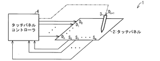
- FIG. 1 is a block diagram showing a schematic configuration of a touch panel system 1 of the present embodiment.
- the touch panel system 1 includes a touch panel 2, a stylus pen (touch pen) 3, and a touch panel controller 4 that drives the touch panel 2 and the stylus pen 3.
- the touch panel 2 is provided with a plurality (n) of drive lines D 0 to D n extending in the horizontal direction in the drawing in parallel, and the sense line S 0 extending in the vertical direction in the drawing.
- ⁇ S m are provided in parallel a plurality (m pieces).
- Capacitances are provided at locations where the drive lines D 0 to D n and the sense lines S 0 to S m intersect. The above m and n may be the same or different.
- a synchronization signal (first synchronization signal) is simultaneously output from the touch panel controller 4 to each of the drive lines D 0 to D n during the synchronization period, and this synchronization signal is detected by the stylus pen 3. And the touch panel controller 4 are synchronized.
- the touch panel controller 4 drives each of the drive lines D 0 to D n during the touch and pen input detection period, and the capacitance of the capacitance by the touch via each of the sense lines S 0 to S m . Change is to be detected.
- the touch panel controller 4 drives the pen line of the stylus pen 3 with the same waveform that drives the drive line D n + 1 , changes the capacitance on the touch surface of the touch panel 2, The change in the capacitance is detected via each of the sense lines S 0 to S m , and additional information such as whether or not the button provided on the stylus pen 3 is pressed by the user and writing pressure. Is detected by the touch panel controller 4.
- the waveform for driving the pen tip does not necessarily have to be D n + 1 such as D n + 2 .
- the pen tip may be driven with a waveform corresponding to D 0 , or the pen tip may be driven with a waveform after D n + 2 .
- the distance between the touch panel 2 and the stylus pen 3 can be calculated by the touch panel controller 4 from the change in capacitance due to the touch.
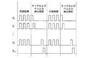
- FIG. 2 is a diagram showing signal waveforms output from the touch panel controller 4 to the drive lines D 0 to D n and a signal waveform D n + 1 for driving the pen tip of the stylus pen 3.
- the same synchronization signal (first synchronization signal) is output from the touch panel controller 4 to the drive lines D 0 to D n during the synchronization period, while during the touch and pen input detection period.
- the drive signals are sequentially output to the drive lines D 0 to D n . That is, during the touch and pen input detection period, the timing at which the drive signal of the drive line D n-1 becomes Low from High, so that the drive signal of the next drive line D n becomes High from Low .
- the pen tip of the stylus pen 3 is driven to change the capacitance on the touch surface of the touch panel 2 and the above-described sense lines S 0 to S m are used to
- the touch panel controller 4 detects a change in capacitance, and detects additional information such as whether or not a button provided on the stylus pen 3 is pressed by the user and writing pressure.
- the driving of the drive lines D 0 to D n and the driving of the pen tip using the signal waveform corresponding to D n + 1 are sequentially driven.
- the M-sequence signal or Hadamard code sequence is used as the code sequence, and the driving of the drive lines D 0 to D n and the driving of the pen tip using the signal waveform corresponding to D n + 1 are performed in parallel.
- the position of the detection target may be detected from the correlation value obtained by performing the correlation calculation of the code string, and the code string restoration calculation is performed.
- the position of the detection object may be detected from the restoration value.
- FIG. 3 is a diagram illustrating a schematic circuit configuration of the touch panel 2 provided in the touch panel system 1.
- a plurality (n) of drive lines D 0 to D n extending in the left-right direction in the drawing are provided in parallel, and cross the drive lines D 0 to D n in the drawing.
- a plurality (m) of sense lines S 0 to S m extending in the vertical direction are provided in parallel.
- Capacitances C 00 to C nm are provided at locations where the drive lines D 0 to D n and the sense lines S 0 to S m intersect.
- the above m and n may be the same or different.
- the stylus pen 3 When the stylus pen 3 approaches the touch surface of the touch panel 2, the stylus pen 3 detects the synchronization signal output from the touch panel controller 4 to each of the drive lines D 0 to D n and is synchronized with the touch panel controller 4.
- the touch panel controller 4 drives each drive line D 0 to D n and touches the above-described touch line via each sense line S 0 to S m. A change in capacitance is detected, and a touch position and / or a distance between the touch panel 2 and the stylus pen 3 is calculated.
- the pen tip of the stylus pen 3 is driven with a waveform corresponding to the drive line D n + 1 to change the electrostatic capacitance on the touch surface of the touch panel 2, and each sense line S 0 to S The change in the capacitance is detected via m , and the touch panel controller 4 detects additional information such as whether or not a button provided on the stylus pen 3 is pressed by the user and writing pressure. It has become.
- the stylus pen 3 of the present embodiment has, for example, a writing pressure sensor for detecting writing pressure, and a writing pressure signal from the writing pressure sensor is output while synchronizing with the touch panel controller 4. It is like that.
- the stylus pen 3 is not necessarily limited thereto, and may not include a writing pressure sensor for detecting writing pressure.
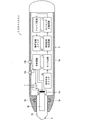
- FIG. 4 is a cross-sectional view showing the configuration of the stylus pen 3.
- the stylus pen 3 includes a pen body 5 that is held by a user and has a conductive grip portion 5 a formed in a substantially cylindrical shape so that the user can hold it by hand.
- a pen tip portion 6 that is pressed against the touch panel 2 at the time of a touch operation is provided at the tip of.
- the pen tip portion 6 is provided on the back side of the pen tip shaft 6b, a pen tip shaft 6b, insulators 6c and 6c that hold the pen tip cover 6a in an axially movable manner, and a pen tip shaft 6b.
- a writing pressure sensor 6d is provided on the back side of the pen tip shaft 6b, a pen tip shaft 6b, insulators 6c and 6c that hold the pen tip cover 6a in an axially movable manner, and a pen tip shaft 6b.
- the pen tip cover 6a is made of an insulating material, and the pen tip shaft 6b is made of a conductive material, for example, a metal or a conductive synthetic resin material.
- the writing pressure sensor 6d is composed of, for example, a semiconductor piezoresistive pressure sensor, and a semiconductor strain gauge is formed on the surface of a diaphragm (not shown). Therefore, when the pen tip cover 6a of the pen tip portion 6 is pressed against the touch panel 2 during the touch operation, the pen tip shaft 6b is pushed through the pen tip cover 6a to press the surface of the diaphragm of the writing pressure sensor 6d, Thereby, a change in electric resistance due to the piezoresistance effect generated by the deformation of the diaphragm is converted into an electric signal. Thereby, the writing pressure in the stylus pen 3 can be detected. Furthermore, the principle of pen pressure detection is not necessarily limited to this, and other detection principles can be employed.
- the pen body 5 includes a connection switch 7, a control circuit 8, operation change-over switches 9 a and 9 b, a sense circuit 10, a synchronization signal detection circuit 11, a timing adjustment circuit 12, and a drive circuit 13. Is provided. Furthermore, the connection switch 7 can be omitted. When the connection switch 7 is omitted, the output of the control circuit 8 is connected to the pen tip shaft 6b.
- connection switch 7 is an electronic switch composed of a field effect transistor (FET) or the like, and is turned on / off by the control circuit 8.
- FET field effect transistor
- the connection switch 7 is off, the pen tip cover 6 a is electrically disconnected from the grip portion 5 a of the pen body 5.
- the touch panel system 1 does not recognize the proximity / contact of the stylus pen 3 even if the pen tip cover 6 a is brought close to the touch panel 2.
- the connection switch 7 when the connection switch 7 is turned on, the pen tip cover 6a is electrically connected to the grip portion 5a of the pen body 5 via the pen tip shaft 6b, and the human body is connected to the pen tip cover 6a via the grip portion 5a.
- Conduct As a result, since the human body has a relatively large capacitance, when the stylus pen 3 approaches or comes into contact with the touch panel 2, the charges accumulated in the aforementioned capacitances C 00 to C nn of the touch panel 2 change.
- the touch panel system 1 can detect the touch state of the stylus pen 3.
- the stylus pen 3 is provided with, for example, a push-type first operation switch 14a and a second operation switch 14b. By pressing the first operation switch 14a and the second operation switch 14b, the first operation switch 14a and the second operation switch 14b are pressed.
- the functions assigned to the first operation switch 14 a and the second operation switch 14 b are executed via the control circuit 8. Examples of the function assigned to the first operation switch 14a include an eraser function. The eraser function can be turned on / off with the first operation switch 14a. Further, as a function assigned to the second operation switch 14b, for example, a right click function of the mouse can be cited, and the right click function of the mouse can be turned on / off by the second operation switch 14b. is there.
- the eraser function and the right-click function of the mouse are examples, and are not limited to the eraser function and the right-click function of the mouse. It is also possible to add other functions by providing other operation switches.
- the touch position of the stylus pen 3 on the touch panel 2 is detected by touching the stylus pen 3 on the touch panel 2 with the connection switch 7 of the stylus pen 3 turned on.
- the pen tip of the stylus pen 3 is driven with a waveform corresponding to the drive line D n + 1 or the like, and the touch panel 2.
- the capacitance on the touch surface is changed, the change in the capacitance is detected via each of the sense lines S 0 to S m, and the button provided on the stylus pen 3 is pressed by the user.
- the touch panel controller 4 detects additional information such as the status and writing pressure.
- the stylus pen 3 of the present embodiment transmits and receives signals to and from the touch panel controller 4 wirelessly. Therefore, the pen tip 6 is driven in the same pattern as driving the virtual drive line D n + 1 so as to match the drive timing of the drive lines D 0 to D n in the touch panel controller 4.
- the stylus pen 3 is provided with a drive circuit 13 so as to be driven in the same manner as the driver of the touch panel controller 4.
- the driving of the drive lines D 0 to D n in the touch panel controller 4 is based on the driving timing generated by the timing generator 17 (FIG. 6). For this reason, the stylus pen 3 must also be operated in synchronization with the timing when the touch panel controller 4 is driven. Therefore, in the stylus pen 3 of the present embodiment, by providing the sense circuit 10, the synchronization signal detection circuit 11, and the timing adjustment circuit 12, the stylus pen 3 detects a dedicated synchronization signal driven by the touch panel controller 4, The timing of the dedicated synchronization signal of the touch panel controller 4 and the timing of the pen synchronization signal generated by the timing adjustment circuit 12 in the stylus pen 3 are made to coincide.
- the stylus pen 3 detects the dedicated synchronization signal generated by the timing generator 17 (FIG. 6) of the touch panel controller 4 by the sense circuit 10 and the synchronization signal detection circuit 11.
- the driving operation of the stylus pen 3 is a synchronization for detecting the synchronization signal from the touch panel controller 4 by the sense circuit 10 and the synchronization signal detection circuit 11 with the operation switch 9a turned on and the operation switch 9b turned off.
- the signal detection period, the preparation period, and the operation changeover switch 9a are turned off, and the operation changeover switch 9b is turned on and the drive circuit 13 drives the pen tip unit 6 to drive the pen tip unit 6 to be configured by repeating three periods. Yes.
- the synchronization signal detection period is a waiting period for detecting a bit pattern representing a synchronization waveform, and is a period in which the pen tip unit 6 is turned off and a synchronization signal pattern is detected from the pen tip signal waveform.
- the preparatory period is a preparatory period for starting to drive the pen tip in synchronization with the touch panel controller 4 after detecting the synchronization signal pattern, and is a period for interpreting additional information that takes a drive start timing.
- the drive mode period is a period in which the pen tip section 6 is driven by the drive circuit 13 and is a period in which the pen tip section 6 is driven while finely adjusting the edge of the drive waveform so as to match the drive timing of the touch panel controller 4. is there.
- the drive circuit 13 of the stylus pen 3 is driven in accordance with the drive timing of the touch panel controller 4.
- FIG. 5 is a diagram illustrating a correspondence relationship between the magnitude of the synchronization signal detected by the stylus pen 3 and the magnitude of the touch response of the stylus pen 3 to the touch panel 2 detected by the touch panel controller 4.
- FIG. 5A is a diagram showing a case where the touch surface of the touch panel 2 and the stylus pen 3 are relatively far apart.
- the stylus pen 3 hardly detects the waveform of the synchronization signal.
- the magnitude of the touch response of the stylus pen 3 to the touch panel 2 detected by the touch panel controller 4 is also determined as having no touch reaction because the touch surface of the touch panel 2 and the stylus pen 3 are relatively far apart.
- FIG. 5B is a diagram illustrating a case where the touch surface of the touch panel 2 and the stylus pen 3 are relatively close to each other.
- the stylus pen 3 detects a waveform of a small synchronization signal. .
- the magnitude of the touch response of the stylus pen 3 to the touch panel 2 detected by the touch panel controller 4 is determined to be a small touch response because the touch surface of the touch panel 2 and the stylus pen 3 are relatively close to each other.
- FIG. 5C is a diagram showing a case where the touch surface of the touch panel 2 and the stylus pen 3 are in contact with each other.
- the stylus pen 3 detects a waveform of a large synchronization signal. .
- the magnitude of the touch reaction of the stylus pen 3 to the touch panel 2 detected by the touch panel controller 4 is determined to be a large touch reaction because the touch surface of the touch panel 2 and the stylus pen 3 are in contact with each other.
- the magnitude of the touch response of the stylus pen 3 to the touch panel 2 detected by the touch panel controller 4, that is, the distance between the touch panel 2 and the stylus pen 3 is determined during the touch and pen input detection period shown in FIG.
- Each of the drive lines D 0 to D n is driven, and the change in the capacitance due to the touch is detected and calculated through each of the sense lines S 0 to S m .
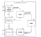
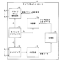
- FIG. 6 is a diagram showing a schematic configuration of the touch panel controller 4 provided in the touch panel system 1.
- the touch panel controller 4 includes a drive line drive circuit 15, a sense amplifier 16, a timing generator 17, a control unit 18, an AD converter 19, and a processing unit 20. Yes.
- the drive line drive circuit 15 is a circuit that outputs the synchronization signal generated based on the clock signal CL generated by the timing generator 17 and the drive signal to each of the drive lines D 0 to D n .
- the sense amplifier 16 is a circuit that acquires capacitance data via the sense lines S 0 to S m based on the clock signal CL generated by the timing generator 17 and the drive signal, and sends the capacitance data to the AD converter 19. It is.
- a clock signal CL and a synchronization signal are generated based on the clock signal CL and sent to the drive line drive circuit 15, the sense amplifier 16, the control unit 18, and the like.
- the capacity data is converted into digital data and then sent to the processing unit 20.
- control unit 18 determines whether to output a thinning signal to the drive line driving circuit 15 based on the magnitude data of the touch reaction (information on the distance between the touch panel 2 and the stylus pen 3). That is, if the touch response magnitude data is equal to or greater than a predetermined value, a thinning signal is output, and if the touch response magnitude data is less than the predetermined value, the touch response magnitude data is output without being thinned.
- processing unit 20 performs processing corresponding to the determined input operation based on the capacity data regarding the touch position, the magnitude data of the touch response, and the additional information.
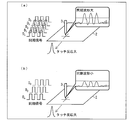
- FIG. 7 is a diagram for explaining the case where the synchronization signal output is thinned out and not performed in the control unit of the touch panel controller 4 provided in the touch panel system 1.
- FIG. 7A shows a case where the control unit 18 outputs without thinning out.
- a synchronization signal is output to all the drive lines D 0 to D n , and the touch panel is displayed.
- the stylus pen 3 detects a waveform of a large synchronization signal.
- FIG. 7B shows a case where the control unit 18 outputs a thinning signal.
- the synchronization signal is output only to a predetermined drive line determined in advance.
- the synchronization signal is output only to the even-numbered drive lines among the drive lines D 0 to D n .
- the waveform of the synchronization signal detected by the stylus pen 3 is relatively small.
- a waveform of such a relatively small synchronization signal exceeds a predetermined reference value and can be detected by the sense circuit 10 and the synchronization signal detection circuit 11 of the stylus pen 3.
- the synchronization signal is output only to the even-numbered drive lines in the drive lines D 0 to D n , but the present invention is not limited to this, and the odd-numbered rows are not limited to this.
- a synchronization signal may be output only to the drive line.
- the stylus pen 3 can detect a synchronization signal having a predetermined intensity or more regardless of the position on the touch surface of the touch panel 2, J of I
- the drive line may be thinned out at an arbitrary ratio such as thinning out (I> J).
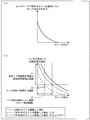
- FIG. 8 is a diagram for explaining how many drive lines should be thinned out of the drive lines D 0 to D n when the control unit 18 outputs a thinning signal.
- FIG. 8A shows the touch panel controller 4 that drives each of the drive lines D 0 to D n during the touch and pen input detection period, and touches each sense line S 0 to S m. It is a figure which shows the relationship between the magnitude
- the magnitude data of the touch reaction detected by the touch panel controller 4 and the height of the hover are associated as illustrated.
- Figure 8 (b) is a diagram showing a relationship between the amplitude and the hover height of the synchronizing signal received at the pen tip of stylus pen 3 (the distance between the stylus pen 3 and the touch panel 2), the drive lines D 0 ⁇ As the number of synchronization signals output decreases during D n , the height of the hover at which the synchronization signal can be detected tends to decrease.
- the range (hover detection range) A in which the approach of the stylus pen 3 is desired to be detected and the range B to be used in the touch operation are determined.
- the range C of the sync signal amplitude that can be detected stably is obtained from the characteristics of the touch panel system 1.
- the minimum number that can be thinned out can be determined from the range A and the range C in the drawing, and the maximum number that can be thinned out can be determined from the range B and the range C in the drawing.
- the number of thinned-out signals is determined from touch response magnitude data that is data related to the height of the hover (distance between the stylus pen 3 and the touch panel 2), and the thinned-out signal is driven to the drive line. It outputs to the drive circuit 15 (refer FIG. 6).
- a thinning signal for driving only Q drive lines out of P is output to the drive line drive circuit 15 To do.
- the height of the hover (distance between the stylus pen 3 and the touch panel 2) is equal to or greater than the range (hover detection range) A in which the approach of the stylus pen 3 is desired to be detected, a thinning signal for driving all the drive lines is sent to the drive line. Output to the drive circuit 15.
- the stylus pen 3 and the touch panel controller 4 are stably synchronized, and the drive timing of the stylus pen 3 and the touch panel controller 4 that drives the touch panel 2 is synchronized.
- the touch panel system 1 that can suppress power consumption and can be driven with low power consumption can be realized.
- I and J and P and Q are values related to the drive lines D 0 to D n in the present embodiment, and therefore I ⁇ n, J ⁇ n, and I > J, P> Q, and P / Q> I / J depending on the signal strength.
- the number of drive lines for outputting a synchronization signal is arbitrarily set to be between J out of I and Q out of P.
- the changing configuration can be realized using a function or a lookup table.
- FIG. 9 is a diagram showing a schematic configuration of the touch panel controller 4a provided in the touch panel system of the present embodiment.
- control unit 18a provided in the touch panel controller 4a receives the touch reaction magnitude data (distance between the stylus pen 3 and the touch panel 2) detected from the processing unit 20 from the change in capacitance due to the touch. ).
- the touch coordinate data is also received from the processing unit 20, and in the drive lines D 0 to D n , the drive line in the area adjacent to the touch coordinate data is received. Only a thinning signal for outputting a synchronization signal is output to the drive line driving circuit 15.
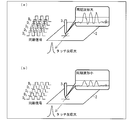
- FIG. 10A shows a case where a synchronization signal is output to the entire drive lines D 0 to D n
- FIG. 10B shows an area adjacent to the touch coordinates in the drive lines D 0 to D n . It is a figure which shows the case where a synchronizing signal is output only to a drive line.
- the synchronization period is 1 msec
- the touch and pen input detection period is 9 msec (see FIG. 2)
- the moving speed of the stylus pen 3 is 1000 mm / sec (the stylus to be supported based on the specifications of the touch panel system) If the pitch of the drive line D 0 to D n is 5 mm, the next touch coordinate detected after 10 msec from the first detected touch coordinate of the stylus pen 3 is the drive line D 0. the possibility that moves by two pins of ⁇ D n.
- the stylus pen 3 and the touch panel controller 4a are stably synchronized, and the drive timing of the stylus pen 3 and the touch panel controller 4a that drives the touch panel 2 is synchronized.
- a touch panel system that can suppress power consumption and can be driven with low power consumption can be realized.
- this Embodiment can be used when the stylus pen 3 approaches the touch surface of the touch panel 2 to such an extent that touch coordinates can be detected, it can also be combined with the above-described Embodiment 1.
- the number of drive lines that output the synchronization signal can be used as the minimum stage.
- Embodiment 3 of the present invention will be described with reference to FIGS.
- the touch panel controller 4b of the touch panel system of the present embodiment is different from the above-described first and second embodiments in that it includes a control unit 18b that adjusts the voltage of the synchronization signal.
- Other configurations are as described in the first and second embodiments.
- members having the same functions as those shown in the drawings of Embodiments 1 and 2 are given the same reference numerals, and descriptions thereof are omitted.
- FIG. 11 is a diagram showing a schematic configuration of the touch panel controller 4b provided in the touch panel system of the present embodiment.
- control unit 18b provided in the touch panel controller 4b is a touch reaction magnitude data (distance between the stylus pen 3 and the touch panel 2) detected from the change in capacitance due to the touch from the processing unit 20. And outputs a voltage adjustment signal for adjusting the voltage of the synchronization signal to the drive line drive circuit 15 in accordance with the magnitude of the touch response.
- FIG. 12A shows a case where a synchronous signal having a relatively high voltage value when rising is output to the entire drive lines D 0 to D n
- FIG. 12B shows the drive line D 0.
- FIG. 11 is a diagram illustrating a case where a synchronization signal having a relatively low voltage value when rising is output to all of D n .
- the magnitude of the waveform of the synchronization signal detected by the stylus pen 3 is smaller than that in the case of FIG. The standard value is exceeded.
- the voltage value of the synchronization signal is lowered, and the synchronization signal whose voltage value is relatively low when it rises (at the time of High).
- the power consumption consumed when synchronizing the drive timing of the stylus pen 3 and the touch panel controller 4b for driving the touch panel 2 is suppressed. It is possible to realize a touch panel system that can be driven with low power consumption.
- the configuration of this embodiment can also be used in combination with Embodiments 1 and 2 described above. Further, the number of drive lines in FIG. The relationship between the amplitude of the synchronization signal newly received by the pen tip of the stylus pen 3 and the height of the hover (distance between the stylus pen 3 and the touch panel 2) is obtained, and the magnitude data of the touch response (stylus pen) Depending on the distance between the touch panel 2 and the touch panel 2, the step of lowering the voltage value of the synchronization signal may be made into a plurality of steps.
- the touch panel controller 4c of the touch panel system according to the present embodiment is different from the above first to third embodiments in that it includes a control unit 18c that outputs a drive pattern selection signal of a synchronization signal.
- Other configurations are as described in the first to third embodiments.
- members having the same functions as those shown in the drawings of Embodiments 1 to 3 are given the same reference numerals, and descriptions thereof are omitted.
- FIG. 13 is a diagram showing a schematic configuration of the touch panel controller 4c provided in the touch panel system of the present embodiment.
- the control unit 18c provided in the touch panel controller 4c is a touch reaction magnitude data (distance between the stylus pen 3 and the touch panel 2) detected from the change in capacitance due to the touch from the processing unit 20. And outputs a drive pattern selection signal of a synchronization signal for selecting a drive pattern of the synchronization signal to the drive line drive circuit 15 according to the magnitude of the touch reaction.
- a synchronization signal drive pattern that shortens the output period of the synchronization signal is selected.
- FIG. 14A shows a case where a synchronization signal is output to the entire drive lines D 0 to D n during a normal period
- FIG. 14B shows the entire drive lines D 0 to D n. The case where the synchronization signal is output for a period shorter than usual is shown.
- the magnitude of the waveform of the synchronization signal detected by the stylus pen 3 is smaller than that in the case of FIG. The standard value is exceeded.
- the stylus pen 3 and the touch panel controller 4c are selected by selecting a drive pattern of the synchronization signal for outputting the synchronization signal for a shorter period of time within a range in which the stylus pen 3 and the touch panel controller 4b can be stably synchronized.
- the touch panel system that can be driven with low power consumption can be achieved by suppressing the power consumption when synchronizing the drive timing of the stylus pen 3 and the touch panel controller 4c that drives the touch panel 2 while stably synchronizing can do.
- the configuration of this embodiment can also be used in combination with Embodiments 1 to 3 described above, and further, the number of drive lines in FIG. Then, the relationship between the amplitude of the synchronization signal newly received by the pen tip of the stylus pen 3 and the height of the hover (distance between the stylus pen 3 and the touch panel 2) is obtained, and touch response magnitude data (stylus pen 3 and Depending on the distance to the touch panel 2, the step of shortening the output period of the synchronization signal may be made into a plurality of steps.
- the time until the touch detection operation starts may be set as the waiting time. You may set so that a touch detection operation may be started immediately without waiting.
- the waiting time until the start of the touch detection operation is set as a waiting time, an effect of reducing power consumption can be obtained, and if the touch detection operation is set to start immediately without waiting, the touch detection operation An effect of shortening the cycle, that is, an effect of obtaining touch coordinates more frequently can be obtained.
- an M-sequence waveform is used as the waveform of the synchronization signal, for example, when the length of the original waveform is based on 2 N ⁇ 1 bits of M-sequence data, a shorter pattern is used. Is a waveform based on data of the number of bits such as 2 N-1 -1, 2 N-2 -1.
- the touch panel system according to the present embodiment is configured in such a manner that the touch position is detected while the drive lines D 0 to D n and the sense lines S 0 to S k are switched at a constant cycle.
- Other configurations are the same as those described in the first to fourth embodiments.
- members having the same functions as those shown in the drawings of Embodiments 1 to 4 are given the same reference numerals, and descriptions thereof are omitted.
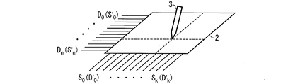
- FIG. 15 is a diagram showing the touch panel 2 and the stylus pen 3 provided in the touch panel system of the present embodiment.
- the drive lines D 0 to D n and the sense lines S 0 to S k provided in the touch panel 2 are switched at a constant cycle, and the drive lines D 0 to D n are switched to the sense lines S 0 ′ to S n ′, and the sense lines S 0 to S k become drive lines D 0 ′ to D k ′.
- k and n may be the same or different.
- FIG. 16A shows the timing when the drive lines D 0 to D n provided on the touch panel 2 are used as drive lines
- FIG. 16B shows the sense lines S 0 to D provided on the touch panel 2. The timing at which S k is used as a drive line is shown.
- the stylus pen 3 is output from the touch panel controller 21 to the drive lines D 0 to D n or the drive lines D 0 ′ to D k ′ by approaching the touch surface of the touch panel 2.
- the stylus pen 3 detects the synchronized signal, and the touch panel controller 21 and the stylus pen 3 are synchronized.
- the touch panel controller 21 drives each drive line D 0 to D n (D 0 ′ to D k ′) and detects each sense line S 0 to S k (S) during the touch and pen input detection period. 0 ′ to S n ′), the change in the capacitance due to the touch is detected.
- the pen tip of the stylus pen 3 is driven with a waveform corresponding to the drive line D n + 1 or D ′ k + 1, etc., and the capacitance on the touch surface of the touch panel 2 is changed to detect each sense.
- the change in electrostatic capacitance is detected via the lines S 0 to S k (S 0 ′ to S n ′), and whether the button provided on the stylus pen 3 by the user is pressed or the writing pressure
- the touch panel controller detects additional information such as.
- the distance between the touch panel 2 and the stylus pen 3 can be calculated from the change in capacitance due to touch by the touch panel controller 21.
- FIG. 17 is a diagram showing a schematic configuration of the touch panel controller 21 provided in the touch panel system of the present embodiment.
- the touch panel controller 21 includes an AD converter 19, a processing unit 20, a multiplexer 22, a drive line driving circuit 23, a sense amplifier 24, a timing generator 25, and a control unit 26. Is provided.
- the multiplexer 22 changes the target lines connected to the drive line drive circuit 23 from the drive lines D 0 to D n (D 0 ′ to D k ′) to the drive lines D 0 ′ to D k ′ (D 0 to At the same time as switching to D n ), the target lines connected to the sense amplifier 24 are changed from the sense lines S 0 to S k (S 0 ′ to S n ) to the sense lines S 0 ′ to S n ′ (S 0 to S k). ).
- the multiplexer 22 is a connection switching circuit that switches connection between a plurality of inputs and a plurality of outputs.
- FIG. 18 is a diagram illustrating an example of signals output from the touch panel controller 21 to the drive lines D 0 to D n and the drive lines D 0 ′ to D k ′.
- the drive lines D 0 to D n (sense lines S 0 ′ to S k ′) and the drive lines D 0 ′ to D k ′ (sense lines S 0 to S n ) are touched and A signal in which the pen input detection period and the sensing period are alternately present at a predetermined period is output.
- the synchronization waveform is also detected in the synchronization period immediately after the touch and pen input detection period (immediately before the sensing period). In the present embodiment, this is the drive line drive circuit 23.
- the synchronization signal is output from the multiplexor 22
- the synchronization signal is output to all of the drive lines D 0 to D n and the drive lines D 0 ′ to D k ′ using the multiplexer 22. is there.
- the drive lines D 0 to D n and the drive lines D 0 ′ to A synchronizing signal may be alternately output with D k ′.
- control unit 26 provided in the touch panel controller 21 receives the touch response magnitude data (the distance between the stylus pen 3 and the touch panel 2) from the processing unit 20, and the touch response If the size is such that touch coordinates can be detected, touch coordinate data is also received from the processing unit 20.
- control unit 26 outputs a thinning signal for outputting a synchronization signal only to the drive line in the area adjacent to the touch coordinates in the drive lines D 0 to D n and the drive lines D 0 ′ to D k ′.
- the synchronization period is 1 msec
- the touch and pen input detection period is 9 msec
- the movement speed of the stylus pen 3 is 1000 mm / sec (the maximum movement of the stylus pen 3 to be supported based on the specifications of the touch panel system) Speed)
- the pitch of the drive lines D 0 to D n and the drive lines D 0 ′ to D k ′ is 5 mm
- the drive lines D 0 to D n and the sense lines S 0 to S k are used to
- the next touch coordinates detected after 10 msec using the drive lines D 0 ′ to D k ′ and the sense lines S 0 ′ to S n ′ from the first detected touch coordinates are the drive lines D 0 to D n.
- the first detected touch coordinates of the stylus pen 3 are represented as drive lines D n-3.
- the drive that outputs the synchronization signal after detecting the touch coordinates may be output only to the lines D n-2 to D n-7 or the drive lines D k-2 ′ to D k-7 ′.
- the stylus pen 3 and the touch panel controller 21 are stably synchronized, and the drive timing of the stylus pen 3 and the touch panel controller 21 that drives the touch panel 2 is synchronized.
- a touch panel system that can suppress power consumption and can be driven with low power consumption can be realized.
- the configuration of the second embodiment described above is combined with the configuration of detecting the touch position while the drive lines D 0 to D n and the sense lines S 0 to S k are switched at a constant cycle.
- the first, third, and fourth embodiments described above are combined with the configuration for detecting the touch position while the drive lines D 0 to D n and the sense lines S 0 to S k are switched at a constant cycle.
- a touch panel system includes a touch panel having capacitance respectively formed at intersections of a plurality of first signal lines and a plurality of second signal lines, a touch panel controller, and a pen.
- a first synchronization signal for synchronizing with the controller is output, a drive signal is output to one of the first signal line and the second signal line after the first synchronization signal, and the drive signal
- a detection signal for detecting the touch position is read from each of the other of the first signal line and the second signal line.
- a distance between the pen and the touch panel is calculated during a period in which the drive signal is output.
- the touch panel controller The second synchronizing signal whose driving power is smaller than the driving power when the first synchronizing signal is output, the first signal line and / or the second signal line after the period during which the driving signal is output. It is the structure which outputs.
- the touch panel controller drives when outputting the first synchronization signal.
- a second synchronization signal whose driving power is lower than the power is output to the first signal line and / or the second signal line after a period during which the driving signal is output.
- the touch panel controller when the touch panel controller outputs the second synchronization signal, the touch panel controller can detect the second synchronization signal with the pen so as to detect the second synchronization signal.
- a configuration may be employed in which the second synchronization signal is output to only some selected signal lines in each and / or the plurality of second signal lines.
- the second synchronization signal is received in each of the first signal lines and / or each of the plurality of second signal lines so that the second synchronization signal can be detected by the pen. Since it is output only to some selected signal lines, it is possible to suppress the power consumed when synchronizing the driving timing of the pen and the touch panel controller, and to realize a touch panel system that can be driven with low power consumption.
- the touch panel controller when the touch panel controller outputs the second synchronization signal, the touch panel in each of the first signal lines and / or each of the second signal lines.
- the second sync signal may be output only to the first signal line and / or the second signal line adjacent to the position.
- the second synchronization signal may be generated by the first signal line and / or the second signal adjacent to the touch position in each of the first signal lines and / or each of the second signal lines. Since the signal is output only to the signal line, it is possible to suppress the power consumed when synchronizing the driving timing of the pen and the touch panel controller, and to realize a touch panel system that can be driven with low power consumption.
- the voltage value at the rising edge of the second synchronization signal is smaller than the voltage value at the rising edge of the first synchronization signal.
- the output period of the second synchronization signal is preferably shorter than the output period of the first synchronization signal.
- the synchronization period is shortened.
- the time until the start of the touch detection operation may be set as a waiting time, or the touch detection operation may be set to start immediately without waiting.
- the waiting time until the start of the touch detection operation is set as a waiting time, an effect of reducing power consumption can be obtained, and if the touch detection operation is set to start immediately without waiting, the touch detection operation An effect of shortening the cycle, that is, an effect of obtaining touch coordinates more frequently can be obtained.
- the predetermined value related to the distance between the pen and the touch panel detects the range of the amplitude of the synchronization signal that can be stably synchronized and the approach of the pen. You may obtain
- the first signal line and / or the second signal line adjacent to the touch position is an amount by which the pen moves before the second synchronization signal is output. It is preferable to be determined by
- the present invention can be suitably used for a touch panel system including a touch panel, a touch panel controller, and a touch pen.
Landscapes
- Engineering & Computer Science (AREA)
- General Engineering & Computer Science (AREA)
- Theoretical Computer Science (AREA)
- Human Computer Interaction (AREA)
- Physics & Mathematics (AREA)
- General Physics & Mathematics (AREA)
- Position Input By Displaying (AREA)
Abstract
Description
本発明の一実施形態について図1~図8に基づいて説明すれば、以下のとおりである。
(タッチパネルシステムの構成)
図1は、本実施の形態のタッチパネルシステム1の概略構成を示すブロック図である。
(タッチパネルの構成)
図3は、タッチパネルシステム1に備えられたタッチパネル2の概略的な回路構成を示す図である。
本実施の形態のスタイラスペン3は、例えば、筆圧を検知するための筆圧センサを有しており、この筆圧センサからの筆圧信号は、タッチパネルコントローラ4と同期を取りながら出力されるようになっている。ただし、スタイラスペン3は、必ずしもこれに限らず、筆圧を検知するための筆圧センサを有していなくてもよい。
ところで、本実施の形態のスタイラスペン3は、無線にてタッチパネルコントローラ4と信号の送受信を行っている。したがって、タッチパネルコントローラ4におけるドライブラインD0~Dnの駆動のタイミングに合うように仮想のドライブラインDn+1を駆動するのと同じパターンでペン先6を駆動する。そこで、スタイラスペン3では、ドライブ回路13を設けてタッチパネルコントローラ4のドライバと同様に駆動を行うようにしている。
次に、図9および図10に基づいて、本発明の実施の形態2について説明する。本実施の形態のタッチパネルシステムのタッチパネルコントローラ4aにおいては、処理部20からのタッチ反応の大きさと座標データに基づいて、ドライブラインD0~Dn中、どの領域のドライブラインを間引くかを決定する制御部18aを備えている点において、上記の実施の形態1とは異なる。その他の構成については実施の形態1において説明したとおりである。説明の便宜上、上記の実施の形態1の図面に示した部材と同じ機能を有する部材については、同じ符号を付し、その説明を省略する。
次に、図11および図12に基づいて、本発明の実施の形態3について説明する。本実施の形態のタッチパネルシステムのタッチパネルコントローラ4bにおいては、同期信号の電圧を調整する制御部18bを備えている点において、上記の実施の形態1および2とは異なる。その他の構成については実施の形態1および2において説明したとおりである。説明の便宜上、上記の実施の形態1および2の図面に示した部材と同じ機能を有する部材については、同じ符号を付し、その説明を省略する。
次に、図13および図14に基づいて、本発明の実施の形態4について説明する。本実施の形態のタッチパネルシステムのタッチパネルコントローラ4cにおいては、同期信号の駆動パターン選択信号を出力する制御部18cを備えている点において、上記の実施の形態1~3とは異なる。その他の構成については実施の形態1~3において説明したとおりである。説明の便宜上、上記の実施の形態1~3の図面に示した部材と同じ機能を有する部材については、同じ符号を付し、その説明を省略する。
次に、図15~図19に基づいて、本発明の実施の形態5について説明する。本実施の形態のタッチパネルシステムにおいては、ドライブラインD0~DnとセンスラインS0~Skとが一定周期で入れ替わりながらタッチ位置を検出する構成となっている点において、上記の実施の形態1~4とは異なる。その他の構成については実施の形態1~4において説明したとおりである。説明の便宜上、上記の実施の形態1~4の図面に示した部材と同じ機能を有する部材については、同じ符号を付し、その説明を省略する。
本発明の態様1におけるタッチパネルシステムは、複数の第1信号線と複数の第2信号線との交点にそれぞれ形成された静電容量を有するタッチパネルと、タッチパネルコントローラと、ペンと、を備え、上記静電容量の変化からタッチ位置を検出するタッチパネルシステムであって、上記タッチパネルコントローラは、複数の上記第1信号線の各々および/または複数の上記第2信号線の各々に、上記ペンと上記タッチパネルコントローラとを同期させるための第1の同期信号を出力し、上記第1信号線および上記第2信号線の一方の各々に、上記第1の同期信号の後に駆動信号を出力し、上記駆動信号に合わせて上記第1信号線および上記第2信号線の他方の各々から、上記タッチ位置を検出する検出信号を読み出すとともに、上記タッチ位置を検出する検出信号に基づいて、上記駆動信号が出力される期間に、上記ペンと上記タッチパネルとの間の距離を算出し、上記距離が所定値未満である場合には、上記タッチパネルコントローラは、上記第1の同期信号を出力する際の駆動電力よりその駆動電力が小さい第2の同期信号を、上記駆動信号が出力される期間の後に上記第1信号線および/または上記第2信号線に、出力する構成である。
2 タッチパネル
3 スタイラスペン(ペン)
4 タッチパネルコントローラ
4a タッチパネルコントローラ
4b タッチパネルコントローラ
4c タッチパネルコントローラ
5 ペン本体
5a 把持部
6 ペン先部
6a ペン先カバー
6b ペン先軸
6c 絶縁体
6d 筆圧センサ
7 接続スイッチ
8 制御回路
9a 動作切替スイッチ
9b 動作切替スイッチ
10 センス回路
11 同期信号検出回路
12 タイミング調整回路
13 ドライブ回路
14a 第1操作スイッチ
14b 第2操作スイッチ
15 ドライブライン駆動回路
16 センスアンプ
17 タイミングジェネレータ
18 制御部
18a 制御部
18b 制御部
18c 制御部
19 AD変換器
20 処理部
21 タッチパネルコントローラ
22 マルチプレクサ
23 ドライブライン駆動回路
24 センスアンプ
25 タイミングジェネレータ
26 制御部
Cnm 静電容量
Dn ドライブライン(第1信号線または第2信号線)
Sm センスライン(第1信号線または第2信号線)
Sk センスライン(第1信号線または第2信号線)
Claims (5)
- 複数の第1信号線と複数の第2信号線との交点にそれぞれ形成された静電容量を有するタッチパネルと、タッチパネルコントローラと、ペンと、を備え、上記静電容量の変化からタッチ位置を検出するタッチパネルシステムであって、
上記タッチパネルコントローラは、複数の上記第1信号線の各々および/または複数の上記第2信号線の各々に、上記ペンと上記タッチパネルコントローラとを同期させるための第1の同期信号を出力し、上記第1信号線および上記第2信号線の一方の各々に、上記第1の同期信号の後に駆動信号を出力し、上記駆動信号に合わせて上記第1信号線および上記第2信号線の他方の各々から、上記タッチ位置を検出する検出信号を読み出すとともに、
上記タッチ位置を検出する検出信号に基づいて、上記駆動信号が出力される期間に、上記ペンと上記タッチパネルとの間の距離を算出し、
上記距離が所定値未満である場合には、上記タッチパネルコントローラは、上記第1の同期信号を出力する際の駆動電力よりその駆動電力が小さい第2の同期信号を、上記駆動信号が出力される期間の後に上記第1信号線および/または上記第2信号線に、出力することを特徴とするタッチパネルシステム。 - 上記タッチパネルコントローラは、上記第2の同期信号を出力する際には、上記第2の同期信号を上記ペンで検出できるように、上記第1信号線の各々および/または上記第2信号線の各々中、選択された一部の信号線にのみ上記第2の同期信号を出力することを特徴とする請求項1に記載のタッチパネルシステム。
- 上記タッチパネルコントローラは、上記第2の同期信号を出力する際には、上記第1信号線の各々および/または上記第2信号線の各々中、上記タッチ位置に隣接する上記第1信号線および/または上記第2信号線にのみ上記第2の同期信号を出力することを特徴とする請求項1に記載のタッチパネルシステム。
- 上記第2の同期信号の立ち上がり時の電圧値は、上記第1の同期信号の立ち上がり時の電圧値より小さいことを特徴とする請求項1から3の何れか1項に記載のタッチパネルシステム。
- 上記第2の同期信号の出力期間は、上記第1の同期信号の出力期間より短いことを特徴とする請求項1から4の何れか1項に記載のタッチパネルシステム。
Priority Applications (2)
| Application Number | Priority Date | Filing Date | Title |
|---|---|---|---|
| JP2015525242A JP5886478B2 (ja) | 2013-07-05 | 2014-07-01 | タッチパネルシステム |
| US14/899,151 US9727166B2 (en) | 2013-07-05 | 2014-07-01 | Proximity-dependent adjustable-signal touch panel system |
Applications Claiming Priority (2)
| Application Number | Priority Date | Filing Date | Title |
|---|---|---|---|
| JP2013141984 | 2013-07-05 | ||
| JP2013-141984 | 2013-07-05 |
Publications (1)
| Publication Number | Publication Date |
|---|---|
| WO2015002203A1 true WO2015002203A1 (ja) | 2015-01-08 |
Family
ID=52143776
Family Applications (1)
| Application Number | Title | Priority Date | Filing Date |
|---|---|---|---|
| PCT/JP2014/067576 Ceased WO2015002203A1 (ja) | 2013-07-05 | 2014-07-01 | タッチパネルシステム |
Country Status (3)
| Country | Link |
|---|---|
| US (1) | US9727166B2 (ja) |
| JP (1) | JP5886478B2 (ja) |
| WO (1) | WO2015002203A1 (ja) |
Cited By (6)
| Publication number | Priority date | Publication date | Assignee | Title |
|---|---|---|---|---|
| WO2017029836A1 (ja) * | 2015-08-19 | 2017-02-23 | 株式会社ワコム | センサコントローラ、位置指示器、及び位置検出システム |
| WO2018029855A1 (ja) * | 2016-08-12 | 2018-02-15 | 株式会社ワコム | スタイラス及びセンサコントローラ |
| JP2018063733A (ja) * | 2018-01-24 | 2018-04-19 | 株式会社ワコム | センサコントローラ及びスタイラス |
| CN107977112A (zh) * | 2016-10-25 | 2018-05-01 | 乐金显示有限公司 | 触摸显示装置、有源笔、触摸系统、触摸电路和笔识别方法 |
| JP2021043640A (ja) * | 2019-09-10 | 2021-03-18 | 株式会社ワコム | タッチコントローラ及びペン入力システム |
| JPWO2021161701A1 (ja) * | 2020-02-10 | 2021-08-19 |
Families Citing this family (13)
| Publication number | Priority date | Publication date | Assignee | Title |
|---|---|---|---|---|
| JP5973072B2 (ja) * | 2013-06-20 | 2016-08-23 | シャープ株式会社 | タッチパネルコントローラ、集積回路、タッチパネル装置、および電子機器 |
| WO2015113061A1 (en) * | 2014-01-27 | 2015-07-30 | Tactual Labs Co. | Decimation strategies for input event processing |
| US9946391B2 (en) | 2014-11-26 | 2018-04-17 | Synaptics Incorporated | Sensing objects using multiple transmitter frequencies |
| US10088922B2 (en) | 2014-11-26 | 2018-10-02 | Synaptics Incorporated | Smart resonating pen |
| US10180736B2 (en) * | 2014-11-26 | 2019-01-15 | Synaptics Incorporated | Pen with inductor |
| US9830000B2 (en) * | 2014-12-12 | 2017-11-28 | Microsoft Technology Licensing, Llc | Active stylus synchronization |
| US10025440B2 (en) * | 2016-07-13 | 2018-07-17 | Stmicroelectronics Asia Pacific Pte Ltd | Correlated data acquisition among different touch sensors |
| CN109564476B (zh) * | 2016-09-13 | 2022-08-30 | 株式会社和冠 | 模拟电路、位置指示器及系统 |
| EP3525069B1 (en) * | 2016-10-06 | 2021-03-17 | Wacom Co., Ltd. | Stylus and controller |
| US10216333B2 (en) * | 2017-06-30 | 2019-02-26 | Microsoft Technology Licensing, Llc | Phase error compensation in single correlator systems |
| US10564420B2 (en) * | 2017-10-02 | 2020-02-18 | International Business Machines Corporation | Midair interaction with electronic pen projection computing system |
| KR102149105B1 (ko) * | 2019-09-18 | 2020-08-27 | 세종대학교산학협력단 | 혼합현실 기반 3차원 스케치 장치 및 방법 |
| KR20240033560A (ko) | 2022-09-05 | 2024-03-12 | 삼성전자주식회사 | 전자 장치, 액티브 스타일러스 펜 및 그 동기화 방법 |
Citations (2)
| Publication number | Priority date | Publication date | Assignee | Title |
|---|---|---|---|---|
| JP2010067117A (ja) * | 2008-09-12 | 2010-03-25 | Mitsubishi Electric Corp | タッチパネル装置 |
| JP2012022543A (ja) * | 2010-07-15 | 2012-02-02 | Panasonic Corp | タッチパネルシステム |
Family Cites Families (2)
| Publication number | Priority date | Publication date | Assignee | Title |
|---|---|---|---|---|
| US9176630B2 (en) * | 2010-08-30 | 2015-11-03 | Perceptive Pixel, Inc. | Localizing an electrostatic stylus within a capacitive touch sensor |
| TWI469025B (zh) * | 2011-08-25 | 2015-01-11 | Touch panel and its dynamic drive control method |
-
2014
- 2014-07-01 WO PCT/JP2014/067576 patent/WO2015002203A1/ja not_active Ceased
- 2014-07-01 JP JP2015525242A patent/JP5886478B2/ja not_active Expired - Fee Related
- 2014-07-01 US US14/899,151 patent/US9727166B2/en active Active
Patent Citations (2)
| Publication number | Priority date | Publication date | Assignee | Title |
|---|---|---|---|---|
| JP2010067117A (ja) * | 2008-09-12 | 2010-03-25 | Mitsubishi Electric Corp | タッチパネル装置 |
| JP2012022543A (ja) * | 2010-07-15 | 2012-02-02 | Panasonic Corp | タッチパネルシステム |
Cited By (41)
| Publication number | Priority date | Publication date | Assignee | Title |
|---|---|---|---|---|
| US10969914B2 (en) | 2015-08-19 | 2021-04-06 | Wacom Co., Ltd. | Method for sensor controller to detect stylus using repeated transmission of control signals, stylus, and system |
| KR102496591B1 (ko) | 2015-08-19 | 2023-02-07 | 가부시키가이샤 와코무 | 스타일러스가 센서 컨트롤러를 검출하는 방법, 스타일러스, 및 센서 컨트롤러 |
| JPWO2017029836A1 (ja) * | 2015-08-19 | 2017-11-02 | 株式会社ワコム | センサコントローラ、位置指示器、及び位置検出システム |
| US12411580B2 (en) | 2015-08-19 | 2025-09-09 | Wacom Co., Ltd. | Sensor controller, position indicator, and position detecting system |
| US11989379B2 (en) | 2015-08-19 | 2024-05-21 | Wacom Co., Ltd. | Sensor controller, position indicator, and position detecting system |
| CN107850951A (zh) * | 2015-08-19 | 2018-03-27 | 株式会社和冠 | 触控笔检测传感器控制器的方法、触控笔及传感器控制器 |
| JP2018056998A (ja) * | 2015-08-19 | 2018-04-05 | 株式会社ワコム | 位置検出器に用いられるセンサコントローラと位置指示器との間で通信を行う方法、位置指示器、及びセンサコントローラ |
| KR102561546B1 (ko) * | 2015-08-19 | 2023-07-31 | 가부시키가이샤 와코무 | 스타일러스가 센서 컨트롤러를 검출하는 방법, 스타일러스, 및 센서 컨트롤러 |
| KR20180040592A (ko) * | 2015-08-19 | 2018-04-20 | 가부시키가이샤 와코무 | 스타일러스가 센서 컨트롤러를 검출하는 방법, 스타일러스, 및 센서 컨트롤러 |
| KR20230022264A (ko) * | 2015-08-19 | 2023-02-14 | 가부시키가이샤 와코무 | 스타일러스가 센서 컨트롤러를 검출하는 방법, 스타일러스, 및 센서 컨트롤러 |
| JPWO2017029829A1 (ja) * | 2015-08-19 | 2018-06-07 | 株式会社ワコム | スタイラスがセンサコントローラを検出する方法、スタイラス、及びセンサコントローラ |
| US11048366B2 (en) | 2015-08-19 | 2021-06-29 | Wacom Co., Ltd. | Sensor controller, position indicator, and position detecting system |
| EP3340017A4 (en) * | 2015-08-19 | 2019-04-03 | Wacom Co., Ltd. | METHOD FOR DETECTING A SENSOR CONTROL DEVICE THROUGH USE OF AN INPUT PENCIL AND SENSOR CONTROL DEVICE |
| US11556213B2 (en) | 2015-08-19 | 2023-01-17 | Wacom Co., Ltd. | Sensor controller, position indicator, and position detecting system |
| US10627928B2 (en) | 2015-08-19 | 2020-04-21 | Wacom Co., Ltd. | Method for stylus to detect sensor controller using repeated reception of symbols, stylus, and sensor controller |
| US10775910B2 (en) | 2015-08-19 | 2020-09-15 | Wacom Co., Ltd. | Sensor controller, position indicator, and position detecting system |
| JP2020181611A (ja) * | 2015-08-19 | 2020-11-05 | 株式会社ワコム | センサコントローラにより実行される方法、システム、及びスタイラス |
| US10852895B2 (en) | 2015-08-19 | 2020-12-01 | Wacom Co., Ltd. | Sensor controller, position indicator, and position detecting system |
| CN107850951B (zh) * | 2015-08-19 | 2020-12-18 | 株式会社和冠 | 触控笔检测传感器控制器的方法、触控笔及传感器控制器 |
| WO2017029836A1 (ja) * | 2015-08-19 | 2017-02-23 | 株式会社ワコム | センサコントローラ、位置指示器、及び位置検出システム |
| WO2017029829A1 (ja) * | 2015-08-19 | 2017-02-23 | 株式会社ワコム | スタイラスがセンサコントローラを検出する方法、スタイラス、及びセンサコントローラ |
| US10061408B2 (en) | 2016-08-12 | 2018-08-28 | Wacom Co., Ltd. | Stylus and sensor controller |
| JP6282790B1 (ja) * | 2016-08-12 | 2018-02-21 | 株式会社ワコム | スタイラス及びセンサコントローラ |
| WO2018029855A1 (ja) * | 2016-08-12 | 2018-02-15 | 株式会社ワコム | スタイラス及びセンサコントローラ |
| US10459540B2 (en) | 2016-08-12 | 2019-10-29 | Wacom Co., Ltd. | Stylus and sensor controller |
| US11054921B2 (en) | 2016-08-12 | 2021-07-06 | Wacom Co., Ltd. | Stylus and sensor controller |
| US11513641B2 (en) | 2016-10-25 | 2022-11-29 | Lg Display Co., Ltd. | Touch display device, active pen, touch system, touch circuit, and pen recognition method |
| CN107977112A (zh) * | 2016-10-25 | 2018-05-01 | 乐金显示有限公司 | 触摸显示装置、有源笔、触摸系统、触摸电路和笔识别方法 |
| JP2018063733A (ja) * | 2018-01-24 | 2018-04-19 | 株式会社ワコム | センサコントローラ及びスタイラス |
| JP7433005B2 (ja) | 2019-09-10 | 2024-02-19 | 株式会社ワコム | タッチコントローラ及びペン入力システム |
| JP2021043640A (ja) * | 2019-09-10 | 2021-03-18 | 株式会社ワコム | タッチコントローラ及びペン入力システム |
| JP2024040263A (ja) * | 2019-09-10 | 2024-03-25 | 株式会社ワコム | タッチコントローラ |
| US11789563B2 (en) | 2019-09-10 | 2023-10-17 | Wacom Co., Ltd. | Touch controller and pen input system |
| JP7615374B2 (ja) | 2019-09-10 | 2025-01-16 | 株式会社ワコム | タッチコントローラ |
| JP2025032019A (ja) * | 2019-09-10 | 2025-03-07 | 株式会社ワコム | タッチコントローラ |
| US12282624B2 (en) | 2019-09-10 | 2025-04-22 | Wacom Co., Ltd. | Touch controller and pen input system |
| JP7839259B2 (ja) | 2019-09-10 | 2026-04-01 | 株式会社ワコム | タッチコントローラ |
| JP7550839B2 (ja) | 2020-02-10 | 2024-09-13 | 株式会社ワコム | ポインタの位置検出方法及びセンサコントローラ |
| JP2024160006A (ja) * | 2020-02-10 | 2024-11-08 | 株式会社ワコム | ポインタの位置検出方法及びセンサコントローラ |
| JP7701535B2 (ja) | 2020-02-10 | 2025-07-01 | 株式会社ワコム | ポインタの位置検出方法及びセンサコントローラ |
| JPWO2021161701A1 (ja) * | 2020-02-10 | 2021-08-19 |
Also Published As
| Publication number | Publication date |
|---|---|
| JP5886478B2 (ja) | 2016-03-16 |
| US20160139732A1 (en) | 2016-05-19 |
| JPWO2015002203A1 (ja) | 2017-02-23 |
| US9727166B2 (en) | 2017-08-08 |
Similar Documents
| Publication | Publication Date | Title |
|---|---|---|
| JP5886478B2 (ja) | タッチパネルシステム | |
| KR102468731B1 (ko) | 터치 구동회로, 터치 표시장치 및 터치 회로의 펜 데이터 인식 방법 | |
| KR102601364B1 (ko) | 터치 센싱 회로, 터치 표시 장치 및 터치 센싱 방법 | |
| EP2515212B1 (en) | Touch screen system and method of driving the same | |
| JP5396333B2 (ja) | タッチパネル装置 | |
| JP6058867B2 (ja) | タッチパネルシステム及び電子機器 | |
| JP6072989B2 (ja) | タッチパネルコントローラ、タッチパネルシステム、およびスタイラスペン | |
| JP6058866B2 (ja) | タッチパネルコントローラ、スタイラスペン、タッチパネルシステム、および電子機器 | |
| US8547115B2 (en) | Touch sensing system, capacitance sensing circuit, and capacitance sensing method | |
| CN104951157B (zh) | 电容式触控装置以及检测主动笔与物体的方法 | |
| US20170192603A1 (en) | Touch detection circuit | |
| KR20150027529A (ko) | 터치 ic 및 이를 이용한 터치 스크린 일체형 표시장치 | |
| JP2019012505A (ja) | タッチ表示装置、ペン、タッチシステム、タッチ回路及びペン認識方法 | |
| US9710075B2 (en) | Touch panel system and electronic device | |
| JP4913859B2 (ja) | タッチパネル装置 | |
| JP2011128857A (ja) | タッチパネル装置 | |
| JP2011243081A (ja) | タッチパネル装置 | |
| CN107621912A (zh) | 在不同触摸传感器之间的相关数据采集 | |
| JPWO2014163107A1 (ja) | タッチパネル位置検出方法、タッチパネルコントローラ、タッチパネルシステム、及び電子機器 | |
| JP4904410B2 (ja) | タッチパネル装置 | |
| CN108475133B (zh) | 触摸板用驱动电路及利用其的触摸感测方法 | |
| CN103558975A (zh) | 输入系统 | |
| WO2016185838A1 (ja) | タッチペン、タッチパネルシステムおよび電子機器 | |
| KR102249035B1 (ko) | 터치 스크린 패널 및 터치 제어장치 | |
| JP5837131B2 (ja) | タッチ位置認識方法及びタッチ位置認識回路 |
Legal Events
| Date | Code | Title | Description |
|---|---|---|---|
| 121 | Ep: the epo has been informed by wipo that ep was designated in this application |
Ref document number: 14819259 Country of ref document: EP Kind code of ref document: A1 |
|
| ENP | Entry into the national phase |
Ref document number: 2015525242 Country of ref document: JP Kind code of ref document: A |
|
| WWE | Wipo information: entry into national phase |
Ref document number: 14899151 Country of ref document: US |
|
| NENP | Non-entry into the national phase |
Ref country code: DE |
|
| 122 | Ep: pct application non-entry in european phase |
Ref document number: 14819259 Country of ref document: EP Kind code of ref document: A1 |