WO2014208307A1 - イオンミリング装置 - Google Patents
イオンミリング装置 Download PDFInfo
- Publication number
- WO2014208307A1 WO2014208307A1 PCT/JP2014/064978 JP2014064978W WO2014208307A1 WO 2014208307 A1 WO2014208307 A1 WO 2014208307A1 JP 2014064978 W JP2014064978 W JP 2014064978W WO 2014208307 A1 WO2014208307 A1 WO 2014208307A1
- Authority
- WO
- WIPO (PCT)
- Prior art keywords
- sample
- ion
- sputtered particle
- ion beam
- adhering member
- Prior art date
- Legal status (The legal status is an assumption and is not a legal conclusion. Google has not performed a legal analysis and makes no representation as to the accuracy of the status listed.)
- Ceased
Links
Images



Classifications
-
- H—ELECTRICITY
- H01—ELECTRIC ELEMENTS
- H01J—ELECTRIC DISCHARGE TUBES OR DISCHARGE LAMPS
- H01J37/00—Discharge tubes with provision for introducing objects or material to be exposed to the discharge, e.g. for the purpose of examination or processing thereof
- H01J37/30—Electron-beam or ion-beam tubes for localised treatment of objects
- H01J37/305—Electron-beam or ion-beam tubes for localised treatment of objects for casting, melting, evaporating, or etching
- H01J37/3053—Electron-beam or ion-beam tubes for localised treatment of objects for casting, melting, evaporating, or etching for evaporating or etching
- H01J37/3056—Electron-beam or ion-beam tubes for localised treatment of objects for casting, melting, evaporating, or etching for evaporating or etching for microworking, e. g. etching of gratings or trimming of electrical components
-
- G—PHYSICS
- G01—MEASURING; TESTING
- G01N—INVESTIGATING OR ANALYSING MATERIALS BY DETERMINING THEIR CHEMICAL OR PHYSICAL PROPERTIES
- G01N1/00—Sampling; Preparing specimens for investigation
- G01N1/28—Preparing specimens for investigation including physical details of (bio-)chemical methods covered elsewhere, e.g. G01N33/50, C12Q
- G01N1/32—Polishing; Etching
-
- H—ELECTRICITY
- H01—ELECTRIC ELEMENTS
- H01J—ELECTRIC DISCHARGE TUBES OR DISCHARGE LAMPS
- H01J37/00—Discharge tubes with provision for introducing objects or material to be exposed to the discharge, e.g. for the purpose of examination or processing thereof
- H01J37/02—Details
- H01J37/20—Means for supporting or positioning the object or the material; Means for adjusting diaphragms or lenses associated with the support
-
- H—ELECTRICITY
- H01—ELECTRIC ELEMENTS
- H01J—ELECTRIC DISCHARGE TUBES OR DISCHARGE LAMPS
- H01J2237/00—Discharge tubes exposing object to beam, e.g. for analysis treatment, etching, imaging
- H01J2237/30—Electron or ion beam tubes for processing objects
- H01J2237/317—Processing objects on a microscale
- H01J2237/31749—Focused ion beam
Definitions
- the present invention relates to an ion milling apparatus for producing a sample observed with a scanning electron microscope or a transmission electron microscope.
- An ion milling device is a device for polishing the surface or cross section of metal, glass, ceramic, etc. by irradiating an argon beam, etc.
- the ion milling apparatus is a processing apparatus that cuts a sample by using a sputtering phenomenon in which atoms on the surface of the sample are ejected from the surface by an ion beam.
- an ion beam shielding plate (hereinafter also referred to as a mask) is placed on the upper surface of the sample other than the processing target position to prevent damage to the sample other than the processing target position due to ion beam scattering, and the sample protrudes from this shielding plate. Let And the cross section of a sample can be processed smoothly by sputter
- Japanese Patent Application Laid-Open No. 2005-135867 discloses a space on the processing surface of the processing sample. Disclosed is a technique for disposing an electrode to generate an electric field and applying 0V or a negative voltage to the sample so that the scattered material generated when the ion beam is irradiated is not deposited on the sample surface.
- Japanese Patent Application Laid-Open No. 2009-14050 discloses a technique for suppressing thermal damage caused by an ion beam by disposing a mask with a sample cooling mechanism even if the sample is vulnerable to heat.
- the present invention has been made in view of such problems, and provides an ion milling apparatus that can effectively suppress reattachment and obtain a clean processed surface of a sample.
- the ion milling apparatus of the present invention is a sputtered particle adhering member that is arranged so as not to interfere with ion beam irradiation in the vicinity of an ion beam irradiation region of a sample mounted on a sample table and adheres sputtered particles generated by ion beam irradiation.
- the temperature of the sputtered particle adhering member is controlled to be lower than the ion beam irradiation region.
- the sputtered particle adhering member has portions extending along the ion beam irradiation direction on both sides of the ion beam irradiation region of the sample.
- the sputtered particle adhering member can be fixed to a sample stage, a sample stage, or a mask disposed between the sample and the ion gun. Or it is good also as a structure which fixes a sputtered particle adhesion member to a vacuum chamber.
- the front schematic diagram which shows schematic structure of the Example of an ion milling apparatus.
- the plane schematic diagram which shows schematic structure of the Example of an ion milling apparatus.
- the schematic diagram which shows the collection state of the sputtered particle by a sputtered particle adhesion member.
- the schematic diagram which shows an example of the sample processing by the conventional ion milling apparatus The schematic diagram which shows an example of the sample processing by the conventional ion milling apparatus.
- the schematic diagram which shows the Example of a temperature control part The front schematic diagram which shows schematic structure of the other Example of an ion milling apparatus.
- a vacuum chamber that is evacuated, an ion gun that irradiates an ion beam, a sample stage that mounts a sample, a sample stage that holds the sample stage, and a sample stage that are mounted in the sample stage are mounted on the sample stage.
- An ion milling device having a sputtered particle adhering member that is disposed in the vicinity of the ion beam irradiation region of the sample so as not to interfere with the ion beam irradiation and adheres sputtered particles generated by the ion beam irradiation is disclosed.
- the embodiment includes a vacuum chamber to be evacuated, an ion gun that irradiates an ion beam accommodated in the vacuum chamber, a sample stage that is accommodated in the vacuum chamber and holds a sample stage on which a sample is mounted,
- An ion milling device having a sputtered particle adhering member having a portion extending along an ion beam for processing a sample is disclosed in which a processing portion of the sample is exposed to an ion beam irradiated from an ion gun .
- the sputtered particle adhering member having a portion extending along the ion beam for processing the sample is used so that the processed portion of the sample is exposed to the ion beam irradiated from the ion gun.
- Ion in an ion milling apparatus that irradiates a processed part of a sample with an ion beam and attaches sputtered particles ejected from the sample to a part of the sputtered particle adhering member that extends along the ion beam. A milling method is disclosed.
- the embodiment discloses that the temperature of the sputtered particle adhering member during ion beam processing is lower than the processed surface of the sample.
- the embodiment discloses that a temperature control unit for controlling the temperature of the sputtered particle adhering member is provided.
- the embodiment discloses that the temperature control unit controls the temperature of the sputtered particle adhering member to be lower than the ion beam irradiation region. Moreover, it discloses that a temperature control part is provided with the container which puts a refrigerant
- the sputtered particle adhering member has portions extending along the ion beam irradiation direction on both sides of the ion beam irradiation region of the sample.
- the embodiment discloses that the sputtered particle adhering member is fixed to the sample stage.
- the embodiment discloses that the sputtered particle adhering member is fixed to the sample stage.
- the embodiment discloses that the sputtered particle adhering member is fixed to a mask disposed between a sample mounted on a sample stage and an ion gun.
- the embodiment discloses that the sputtered particle adhering member is fixed to the vacuum chamber.
- Example 1 and 2 are schematic diagrams showing a schematic configuration of an ion milling apparatus according to the present embodiment.
- FIG. 1 is a schematic front view
- FIG. 2 is a schematic plan view.
- the ion milling apparatus includes an ion gun 104, a vacuum chamber 105, a vacuum exhaust pump 106, a sample stage 107, a sample stage 108, a sputtered particle adhering member 109, and the like.
- the ion beam 103 is emitted from the ion gun 104.
- the inside of the vacuum chamber 105 is controlled to atmospheric pressure or vacuum by a vacuum exhaust pump 106, and the ion gun 104, the sample stage 107, the sample stage 108, and the like can be maintained in a vacuum atmosphere.
- the sample 101 is mounted on the sample stage 107, and the sample stage 107 is held on the sample stage 108.
- the mask 102 is for shielding the ion beam 103 and is held on the sample 101.
- the ion beam 103 scrapes the sample portion protruding from the mask 102.
- the sputtered particle adhering member 109 is held on the mask 102.
- a temperature control unit 110 is connected to the sputtered particle adhering member 109.
- the mask 102, the sample 101, the sample stage 107, and the sample stage 108 are also cooled. Since the temperature control unit 110 cools the sputtered particle adhering member 109, the mask 102, the sample 101, the sample stage 107, and the sample stage 108 in this order, the sputtered particle adhering member 109 has the lowest temperature.
- FIG. 3 is a detailed schematic diagram of the sample, mask, and sputtered particle adhering member held on the sample stage.
- a metal plate 310 connected to the temperature control unit 110 is used as the sputtered particle adhesion member 109 that is disposed in the vicinity of the irradiated region of the ion beam 103 and adheres the sputtered particles 301 that have jumped out of the sample 101 by the ion beam irradiation.
- the sputtered particle adhesion member 109 that is disposed in the vicinity of the irradiated region of the ion beam 103 and adheres the sputtered particles 301 that have jumped out of the sample 101 by the ion beam irradiation.
- the sputtered particle adhesion member 109 that is disposed in the vicinity of the irradiated region of the ion beam 103 and adheres the sputtered particles 301 that have jumped out of the sample 101 by the ion beam irradiation.
- the metal plate 310 is not in contact with the sample 101, and is disposed in the vicinity of the processing surface of the sample 101, that is, near the region where sputtered particles are generated, along the irradiation direction of the ion beam 103 so as not to interfere with the irradiation of the ion beam. Yes.
- the metal plate 310 of this example has a substantially U-shaped shape including two leg portions 310b and 310c and a main body portion 310a connecting the two leg portions 310b and 310c, and has two leg portions. 310b and 310c are bent substantially at right angles to the main body part from the middle.
- the main body portion 310 a is placed on the mask 102 so that the main body portion and the leg portion surround the ion beam 103, and the two bent leg portions 310 b and 310 c are on both sides of the processing surface of the sample 101. Placed away from the sample.
- the metal plate 310 has a property that it is difficult to be sputtered even when the end of the ion beam 103 is irradiated, such as a metal material having high thermal conductivity such as Cu (copper), Al (aluminum), or Ti (titanium).
- the metal material possessed or the upper surface that may be sputtered has a property that it is difficult to be sputtered, and the other part is composed of a composite metal material having a high thermal conductivity and is cooled by the temperature controller 110.
- the metal plate 310 is disposed so as to expose the processed surface of the sample 101 so as not to prevent the irradiation of the ion beam 103 onto the processed surface of the sample 101.
- FIG. 4 is a schematic view showing a state where the sputtered particles 301 are collected by the sputtered particle adhering member 109.
- sputtered particles 301 are generated from the processing surface 302 of the sample 101 irradiated with the ion beam 103.
- the sputtered particles 301 generated by the ion beam irradiation are a processed surface 302 to which heat is applied by irradiating the ion beam 103 and a metal plate 310 having a temperature lower than the periphery thereof, in particular, an ion beam irradiation region of the sample, that is, a processed surface 302.
- the sputtered particle adhering member Adsorbed to the legs 310b and 310c extending along the irradiation direction of the ion beam 103 on both sides of the beam. Therefore, it is possible to perform processing while reducing contamination of the processing surface 302 by the sputtered particles 301.
- the sputtered particle adhering member is held on the mask, but if the sputtered particle adhering member is at a lower temperature than the ion beam irradiation region, the sputtered particle adhering member is held on the sample stage or sample stage. Also good.
- FIG. 5 to 7 are diagrams showing an example of a method for fixing the sputtered particle adhering member.
- FIG. 5 is an explanatory diagram of an example in which the sputtered particle adhering member is fixed to the sample stage.
- an L-shaped fixing portion extending downward is provided at the rear end of the main body portion of the sputtered particle adhering member 109, and the fixing portion is fixed to the sample stage 108 by the fixing screw 121. Fixing of the sputtered particle adhesion member 109 to the sample stage 108 using the fixing screw 121 is performed in a state where the sample stage is taken out of the vacuum chamber 105, and then the sample stage 108 is attached to the vacuum chamber 105.
- FIG. 6 is an explanatory diagram of an example of fixing the sputtered particle adhering member to the mask.
- the rear end of the main body portion of the sputtered particle adhering member 109 is fixed to the mask 102 with a fixing screw 121.
- Fixing the sputtered particle adhesion member 109 to the mask 102 using the fixing screw 121 is performed with the sample stage taken out of the vacuum chamber 105, and then the sample stage 108 is attached to the vacuum chamber 105.
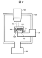
- FIG. 7 is an explanatory diagram of an example in which the sputtered particle adhering member is fixed to the sample stage.
- a fixing portion extending downward is provided at the rear end of the main body portion of the sputtered particle adhering member 109, and the fixing portion is fixed to the sample stage 107 with the fixing screw 121.
- the sputter particle adhesion member 109 is fixed to the sample stage 107 using the fixing screw 121 in a state where the sample stage is taken out of the vacuum chamber 105, and then the sample stage 108 is attached to the vacuum chamber 105.
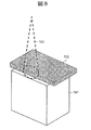
- FIG. 8 and 9 are schematic views showing an example of sample processing by a conventional ion milling apparatus.
- the mask 102 is placed on the sample 101 as shown in FIG. 8 and the ion beam 103 is irradiated, sputtered particles 301 are generated from the processed surface 302 irradiated with the ion beam 103 as shown in FIG. Since the sputtered particles 301 are deposited again on the processed surface 302, the sputtered particles 301 become an obstacle when observing the electron microscope after processing.
- the cooled sputtered particle adhering member as in this embodiment is disposed along the ion beam near the processing surface so as not to interfere with the irradiation of the ion beam, and the sputtered particles are attached to the sputtered particle adhering member and captured.
- spatter particles can be prevented from reattaching to the processed surface, and the processed surface can be kept clean.
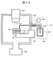
- FIG. 10 is a schematic diagram showing an embodiment of the temperature control unit 110.
- the temperature control unit that cools the sputtered particle adhering member includes a container 501 that contains a refrigerant, a refrigerant 502, and a heat transfer wiring 503 that connects the refrigerant 502 and the sputtered particle adhering member 109.
- the coolant 502 for example, liquid nitrogen, liquid helium, dry ice, or the like can be used.
- the sputtered particle adhering member 109 and the heat transfer wiring 503 connecting the coolant 502 and the sputtered particle adhering member 109 are made of a material having high thermal conductivity such as Cu (copper) or Al (aluminum).
- At least a member having better thermal conductivity than the members around the heat transfer wiring 503 is used. Thereby, the heat of the refrigerant is transmitted through the heat transfer wiring 503 that connects the refrigerant 502 and the sputtered particle adhering member 109, and the sputtered particle adhering member 109 can be cooled.
- FIG. 10 shows an example of a method of cooling using a refrigerant, but the sputtered particle adhering member can be cooled even using a Peltier element or the like. Further, by combining the heater 504, the sputtered particle adhering member 109 can be adjusted to an arbitrary temperature.
- the vacuum chamber 105 is opened to the atmosphere with the sputtered particle adhering member 109 cooled too much, frost adhesion to the sputtered particle adhering member 109 is induced and contamination of the sample processing surface located near the sputtered particle adhering member is caused. There is a risk of connection. Therefore, it is necessary to wait for the temperature of the sputtered particle adhering member 109 to rise to room temperature before opening the vacuum chamber 105 to the atmosphere. Since the temperature control unit 110 connected to the sputtered particle adhering member 109 can realize not only cooling but also heating, the sputtered particle adhering member 109 can be adjusted to about room temperature by heating before being released into the atmosphere. Therefore, the atmosphere can be released immediately after the milling is completed, and the throughput can be improved.
- the sputtered particle adhering member is made of a metal plate.
- the surface of the metal plate may be a flat surface or a rough surface.
- a rod-like or block-like member may be used.
- the sputtered particle adhering member illustrated in FIGS. 3 and 4 has an open structure where the part facing the sample processing surface is open, and the sputtered particles scattered in the vertical direction from the sample processing surface are between the legs of the sputtered particle adhering member.
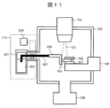
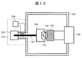
- Example 2 11 and 12 are schematic views showing a schematic configuration of the ion milling apparatus according to the second embodiment.
- FIG. 11 is a schematic front view
- FIG. 12 is a schematic plan view.
- the ion milling apparatus of the present embodiment can cool only the sputtered particle adhering member.
- the major difference from Example 1 is that the sputtered particle adhesion member 109 is attached to the vacuum chamber 105 without being attached to the mask 102 or the sample stage 107. Therefore, the sputtered particle adhering member 109 can be installed independently from the sample 101.
- the support portion 601 of the sputtered particle adhering member 109 also serves as a heat transfer unit that connects the temperature control unit 110 and the sputtered particle adhering member 109. In this embodiment, only the sputtered particle adhering member 109 is controlled in temperature, so that the time required for temperature change is short. Therefore, since the sputtered particle adhering member 109 can be cooled in a short time, the throughput of the apparatus can be improved.
- the shape, structure, material, and the like of the sputtered particle adhering member 109 can be the same as those in the first embodiment.
- the temperature control unit 110 includes a container 501 for containing a refrigerant, a refrigerant 502, a support part (heat transfer part) 601 that connects the refrigerant 502 and the sputtered particle adhesion member 109, and a heater 504.
- a refrigerant 502 for example, liquid nitrogen, liquid helium, dry ice, or the like can be used.
- a material having high thermal conductivity such as Cu (copper) or Al (aluminum) is used.
- a Peltier element or the like may be used for the temperature control unit 110 instead of a refrigerant or a heater.
- the vacuum chamber 105 is opened to the atmosphere with the sputtered particle adhering member 109 cooled too much, frost adhesion to the sputtered particle adhering member 109 is induced and contamination of the sample processing surface located near the sputtered particle adhering member is caused. There is a risk of connection. Therefore, it is necessary to wait for the temperature of the sputtered particle adhering member 109 to rise to room temperature before opening the vacuum chamber 105 to the atmosphere. Since the temperature control unit 110 connected to the sputtered particle adhering member 109 can realize not only cooling but also heating by the heater 504, the sputtered particle adhering member 109 is adjusted to about room temperature by heating before opening to the atmosphere after processing. Can do. Therefore, the atmosphere can be released immediately after the milling is completed, and the throughput can be improved.
- the sputtered particle adhering member 109 since the sputtered particle adhering member 109 is not in contact with the sample 101, the mask 102, the sample stage 107, the sample stage 108, etc., the sample 101 is not affected by the temperature change due to cooling and heating of the sputtered particle adhering member 109. I do not receive it. Further, the mask 102, the sample stage 107, and the sample stage 108 can suppress re-adhesion without requiring modification for attaching the sputtered particle adhering member 109.
- this invention is not limited to said Example, Various modifications are included.
- the above-described embodiments have been described in detail for easy understanding of the present invention, and are not necessarily limited to those having all the configurations described.
- a part of the configuration of a certain embodiment can be replaced with another embodiment, and the configuration of another embodiment can be added to the configuration of a certain embodiment.
Landscapes
- Chemical & Material Sciences (AREA)
- Analytical Chemistry (AREA)
- Physics & Mathematics (AREA)
- Life Sciences & Earth Sciences (AREA)
- Plasma & Fusion (AREA)
- Health & Medical Sciences (AREA)
- Engineering & Computer Science (AREA)
- Biochemistry (AREA)
- General Health & Medical Sciences (AREA)
- General Physics & Mathematics (AREA)
- Immunology (AREA)
- Pathology (AREA)
- Sampling And Sample Adjustment (AREA)
Abstract
試料へのスパッタ粒子の再付着を抑制し、清浄な加工面を得ることを目的として、試料台107に搭載された試料101のイオンビーム照射領域近傍に、イオンビーム103の照射を妨げないように、イオンビームの照射より発生したスパッタ粒子を付着させるスパッタ粒子付着部材109を配置する。スパッタ粒子付着部材は、イオンビーム照射領域より低くなるように温度制御される。
Description
本発明は、走査型電子顕微鏡や透過型電子顕微鏡などで観察される試料を作製するためのイオンミリング装置に関する。
イオンミリング装置は、金属、ガラス、セラミックなどの表面或いは断面を、アルゴンビームを照射するなどして研磨するための装置であり、電子顕微鏡により試料の表面あるいは断面を観察するための前処理装置として好適である。イオンミリング装置は、イオンビームによって試料表面の原子を表面からはじき出すスパッタ現象を用いて、試料を削る加工装置である。試料加工時は、イオンビーム散乱による加工目的位置以外の試料損傷を防ぐため、加工目的位置以外の試料上面にイオンビームの遮蔽板(以下、マスクとも言う)を置き、この遮蔽板から試料を突出させる。そして、突出された試料部分がスパッタされることで試料の断面を平滑に加工できる。
イオンビーム加工において、スパッタ粒子がマスク及び加工面へ再付着して試料にバリが発生することを抑制するために、特開2005-135867号公報には、被加工試料の被加工面上の空間に電界を発生させるための電極を配置し、試料に0Vもしくは負の電圧を印加することにより、イオンビームを照射したときに発生する飛散物質を試料表面に堆積させずに加工を行う技術が開示されている。特開2009-145050号公報には、熱に弱い試料であっても、試料冷却機構の付いたマスクを配置することでイオンビームによる熱ダメージを抑制する技術が開示されている。
イオンミリング装置で試料を加工すると、イオンビームによって削られた物質(以下、スパッタ粒子と言う)の試料への再付着(リデポジション)が起こり、清浄な加工面を取得することが困難となる。特許文献1のようなイオンビーム加工装置でも、試料の断面加工時の再付着の問題が解消されていない。特許文献2のようなイオンビーム加工装置であっても再付着の抑制については言及していない。
本発明は、このような課題を鑑みてなされたものであって、再付着を効果的に抑制し試料の清浄な加工面を取得することができるイオンミリング装置を提供するものである。
本発明のイオンミリング装置は、試料台に搭載された試料のイオンビーム照射領域近傍にイオンビームの照射を妨げないように配置され、イオンビームの照射より発生したスパッタ粒子を付着させるスパッタ粒子付着部材を有する。スパッタ粒子付着部材は、イオンビーム照射領域より低くなるように温度制御される。この構成により、試料やマスクからスパッタされたスパッタ粒子は、スパッタ粒子付着部材に優先的に付着するので、試料加工面への再付着を抑制できる。
スパッタ粒子付着部材は、一例として、試料のイオンビーム照射領域の両側にイオンビームの照射方向に沿って延在する部分を有する。スパッタ粒子付着部材は、試料台、試料ステージ、あるいは試料とイオン銃の間に配置されるマスクなどに固定することができる。あるいは、真空チャンバーにスパッタ粒子付着部材を固定する構造としてもよい。
本発明によれば、イオンミリング装置でイオンビームによって試料やマスクから削られた物質、汚染物質が試料へ再付着することを効果的に抑制でき、清浄な加工面を得ることができる。
上記した以外の、課題、構成及び効果は、以下の実施形態の説明により明らかにされる。
上記した以外の、課題、構成及び効果は、以下の実施形態の説明により明らかにされる。
実施例には、真空排気される真空チャンバーと、真空チャンバーに収容された、イオンビームを照射するイオン銃、試料を搭載する試料台、及び試料台を保持する試料ステージと、試料台に搭載された試料のイオンビーム照射領域近傍にイオンビームの照射を妨げないように配置され、イオンビームの照射より発生したスパッタ粒子を付着させるスパッタ粒子付着部材と、を有するイオンミリング装置を開示する。
また、実施例には、真空排気される真空チャンバーと、真空チャンバーに収容された、イオンビームを照射するイオン銃と、真空チャンバーに収容された、試料を搭載する試料台を保持する試料ステージと、イオン銃から照射されるイオンビームに対して試料の加工部は露出させ、且つ試料を加工するイオンビームに沿って延在する部分を有するスパッタ粒子付着部材と、を有するイオンミリング装置を開示する。
また、実施例には、試料を加工するイオンビームに沿って延在する部分を有するスパッタ粒子付着部材を、イオン銃から照射されるイオンビームに対して試料の加工部が露出されるように試料に対して配置し、試料の加工部にイオンビームを照射し、当該試料から弾き出されたスパッタ粒子を、スパッタ粒子付着部材におけるイオンビームに沿って延在する部分に付着させる、イオンミリング装置におけるイオンミリング加工方法を開示する。
また、実施例には、イオンビーム加工中のスパッタ粒子付着部材の温度を、試料の加工面より低温とすることを開示する。
また、実施例には、スパッタ粒子付着部材の温度を制御する温度制御部を備えることを開示する。
また、実施例には、温度制御部が、スパッタ粒子付着部材の温度をイオンビーム照射領域より低くなるように制御することを開示する。また、温度制御部が、冷媒を入れる容器と、容器中の冷媒とスパッタ粒子付着部材とを繋ぐ伝熱部材とを備えることを開示する。また、温度制御部がスパッタ粒子付着部材を加熱する機能も有することを開示する。また、温度制御部が、真空チャンバーを大気開放するに先だってスパッタ粒子付着部材を加熱することを開示する。
また、実施例には、スパッタ粒子付着部材は試料のイオンビーム照射領域の両側にイオンビームの照射方向に沿って延在する部分を有することを開示する。
また、実施例には、スパッタ粒子付着部材が試料台に固定されることを開示する。
また、実施例には、スパッタ粒子付着部材が試料ステージに固定されることを開示する。
また、実施例には、スパッタ粒子付着部材が試料台に搭載された試料とイオン銃の間に配置されるマスクに固定されることを開示する。
また、実施例には、スパッタ粒子付着部材が真空チャンバーに固定されることを開示する。
以下、図面を参照して本発明の実施の形態を説明する。
[実施例1]
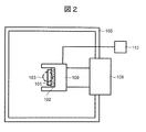
図1及び図2は、本実施例のイオンミリング装置の概略構成を示す摸式図である。図1は正面模式図、図2は平面模式図である。
図1及び図2は、本実施例のイオンミリング装置の概略構成を示す摸式図である。図1は正面模式図、図2は平面模式図である。
本実施例のイオンミリング装置は、イオン銃104、真空チャンバー105、真空排気ポンプ106、試料台107、試料ステージ108、スパッタ粒子付着部材109などから構成されている。イオンビーム103はイオン銃104から照射される。真空チャンバー105は、真空排気ポンプ106によって内部が大気圧又は真空に制御され、イオン銃104、試料台107、試料ステージ108などを真空雰囲気に維持することができる。試料101は試料台107に搭載され、試料台107は試料ステージ108に保持される。マスク102はイオンビーム103を遮蔽するためのものであり、試料101の上に保持されている。イオンビーム103は、マスク102から突出した試料部分を削る。
スパッタ粒子付着部材109は、マスク102の上に保持されている。スパッタ粒子付着部材109には、温度制御部110が接続されている。スパッタ粒子付着部材109を冷却すると、マスク102、試料101、試料台107、試料ステージ108も冷却される。温度制御部110は、スパッタ粒子付着部材109、マスク102、試料101、試料台107、試料ステージ108の順に冷却するため、スパッタ粒子付着部材109が一番の低温になる。
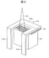
図3は、試料ステージ上に保持された試料、マスク及びスパッタ粒子付着部材の詳細模式図である。ここでは、イオンビーム103の被照射領域近傍に配置され、イオンビーム照射により試料101から飛び出したスパッタ粒子301を付着させるスパッタ粒子付着部材109として、温度制御部110に接続された金属板310を用いた例を示す。金属板310は試料101とは接触せず、イオンビームの照射を妨げないようにイオンビーム103の照射方向に沿って試料101の加工面近傍、すなわちスパッタ粒子の発生する領域の近くに配置されている。本例の金属板310は、2本の脚部310b,310cとその2本の脚部310b,310cを接続する本体部分310aとを備える概略U字状の形状を有し、2本の脚部310b,310cは途中から本体部分に対してほぼ直角に折れ曲がっている。金属板310は、本体部分と脚部とでイオンビーム103を囲むようにして本体部分310aがマスク102の上に載置され、折れ曲がった2本の脚部310b,310cは試料101の加工面の両側に試料から離して配置される。金属板310は、例えばCu(銅),Al(アルミニウム)等、熱伝導率の高い金属材料、若しくはTi(チタン)のようにイオンビーム103の端部が照射されたとしてもスパッタされにくい性質を持つ金属材料、又はスパッタされる可能性のある上面はスパッタされにくい性質を持ち、その他の部分は熱伝導率が高い複合的な金属材料等からなり、温度制御部110によって冷却される。金属板310は、イオンビーム103の、試料101の加工面への照射を妨げないように、試料101の加工面を露出するように配置される。
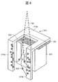
図4は、スパッタ粒子付着部材109によるスパッタ粒子301の捕集状態を示す模式図である。イオンビーム103で加工を行うと、イオンビーム103を照射した試料101の加工面302からスパッタ粒子301が発生する。イオンビーム照射によって発生するスパッタ粒子301は、イオンビーム103を照射することによって熱が加わっている加工面302やその周辺より温度の低い金属板310、特に試料のイオンビーム照射領域、すなわち加工面302の両側にイオンビーム103の照射方向に沿って延在している脚部310b,310cに吸着する。そのため、スパッタ粒子301による加工面302の汚染を低減して加工を行うことができる。本実施例では、スパッタ粒子付着部材はマスクの上に保持されているが、スパッタ粒子付着部材がイオンビーム照射領域より低温であれば、スパッタ粒子付着部材は試料台や試料ステージ上に保持されても良い。
図5から図7は、スパッタ粒子付着部材の固定方法の例を示す図である。
図5は、スパッタ粒子付着部材を試料ステージに固定する例の説明図である。本例では、スパッタ粒子付着部材109の本体部分後端に下方に延在するL字形の固定部を設け、固定部を固定ネジ121によって試料ステージ108に固定する。固定ネジ121を用いたスパッタ粒子付着部材109の試料ステージ108への固定は、試料ステージを真空チャンバー105の外に取り出した状態で行い、その後、試料ステージ108を真空チャンバー105に取り付ける。
図5は、スパッタ粒子付着部材を試料ステージに固定する例の説明図である。本例では、スパッタ粒子付着部材109の本体部分後端に下方に延在するL字形の固定部を設け、固定部を固定ネジ121によって試料ステージ108に固定する。固定ネジ121を用いたスパッタ粒子付着部材109の試料ステージ108への固定は、試料ステージを真空チャンバー105の外に取り出した状態で行い、その後、試料ステージ108を真空チャンバー105に取り付ける。
図6は、スパッタ粒子付着部材をマスクに固定する例の説明図である。本例では、スパッタ粒子付着部材109の本体部分後端をマスク102に固定ネジ121によって固定する。固定ネジ121を用いたスパッタ粒子付着部材109のマスク102への固定は、試料ステージを真空チャンバー105の外に取り出した状態で行い、その後、試料ステージ108を真空チャンバー105に取り付ける。
図7は、スパッタ粒子付着部材を試料台に固定する例の説明図である。本例では、スパッタ粒子付着部材109の本体部分後端に下方に延在する固定部を設け、固定部を固定ネジ121によって試料台107に固定する。固定ネジ121を用いたスパッタ粒子付着部材109の試料台107への固定は、試料ステージを真空チャンバー105の外に取り出した状態で行い、その後、試料ステージ108を真空チャンバー105に取り付ける。
ここで、本実施例のスパッタ粒子付着部材を用いないで加工した従来の試料加工面を比較例として示す。図8、図9は、従来のイオンミリング装置による試料加工の一例を示す模式図である。図8のように試料101の上にマスク102を配置してイオンビーム103を照射すると、図9のようにイオンビーム103を照射した加工面302からスパッタ粒子301が発生する。このスパッタ粒子301は、加工面302に再付着し堆積するため、加工後の電子顕微鏡観察時の障害になる。
一方、本実施例のように冷却したスパッタ粒子付着部材を、イオンビームの照射を妨げないように加工面の近くにイオンビームに沿って配置し、スパッタ粒子をスパッタ粒子付着部材に付着させて捕集することで、加工面へのスパッタ粒子の再付着を防止し、加工面を清浄に維持することができる。
図10は、温度制御部110の実施例を示す模式図である。スパッタ粒子付着部材を冷却する温度制御部は、冷媒を入れる容器501,冷媒502,冷媒502とスパッタ粒子付着部材109を繋ぐ伝熱配線503で構成されている。冷媒502には、例えば、液体窒素,液体ヘリウム,ドライアイス等を用いることができる。また、スパッタ粒子付着部材109、及び冷媒502とスパッタ粒子付着部材109を繋ぐ伝熱配線503には、例えば、Cu(銅),Al(アルミニウム)等、熱伝導率の高い材料を用いる。少なくとも、伝熱配線503の周囲の部材より熱伝導性のよい部材を用いる。これにより、冷媒の熱が、冷媒502とスパッタ粒子付着部材109を繋ぐ伝熱配線503を通して伝わり、スパッタ粒子付着部材109を冷却することができる。
図10では、冷媒を用いて冷却する方法を例としてあげたが、ペルチェ素子等を用いてもスパッタ粒子付着部材の冷却は可能である。また、ヒーター504を組み合わせることによって、スパッタ粒子付着部材109を任意の温度に調整することできる。
また、スパッタ粒子付着部材109を冷却しすぎた状態で真空チャンバー105を大気開放すると、スパッタ粒子付着部材109への霜の付着を誘発し、スパッタ粒子付着部材近傍に位置する試料加工面の汚染へとつながる恐れがある。そのため、真空チャンバー105を大気開放する前にスパッタ粒子付着部材109の温度が室温まで上昇するのを待つ必要がある。スパッタ粒子付着部材109に接続している温度制御部110では冷却だけでなく加熱も実現できるため、大気開放前には加熱によってスパッタ粒子付着部材109を室温程度に調節することができる。そのため、ミリング終了後すぐに大気開放でき、スループットの向上が図れる。
ここでは、スパッタ粒子付着部材を金属板で構成する例を説明した。金属板の表面は平坦面であってもよいし、粗面としてもよい。また、板状以外に、棒状、あるいはブロック状の部材であってもよい。また、図3、図4に例示したスパッタ粒子付着部材は、試料の加工面に対面する部分を開放構造とし、試料加工面から垂直方向に飛散するスパッタ粒子はスパッタ粒子付着部材の脚部の間を通り抜けて自由に流出できるようにしたが、それらのスパッタ粒子も捕集できるように2本の脚部の間を塞ぐ構造としてもよい。
[実施例2]
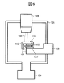
図11及び図12は、実施例2のイオンミリング装置の概略構成を示す摸式図である。図11は正面模式図、図12は平面模式図である。本実施例のイオンミリング装置は、スパッタ粒子付着部材だけを冷却することができる。
図11及び図12は、実施例2のイオンミリング装置の概略構成を示す摸式図である。図11は正面模式図、図12は平面模式図である。本実施例のイオンミリング装置は、スパッタ粒子付着部材だけを冷却することができる。
実施例1との大きな違いは、スパッタ粒子付着部材109をマスク102や試料台107に取り付けず、真空チャンバー105に取り付けていることである。従って、試料101から独立してスパッタ粒子付着部材109を設置することができる。スパッタ粒子付着部材109の支持部601は温度制御部110とスパッタ粒子付着部材109を繋ぐ伝熱部も兼ねている。本実施例では、スパッタ粒子付着部材109だけを温度制御するため、温度変化に掛かる時間が短い。そのため、スパッタ粒子付着部材109を短時間で冷却することができるので、装置のスループットの向上が図れる。スパッタ粒子付着部材109の形状、構造、材質などは実施例1と同様とすることができる。
図示の例では、温度制御部110は、冷媒を入れる容器501,冷媒502,冷媒502とスパッタ粒子付着部材109を繋ぐ支持部(伝熱部)601、及びヒーター504で構成されている。冷媒502には、例えば、液体窒素,液体ヘリウム,ドライアイス等を用いることができる。また、スパッタ粒子付着部材109及び冷媒502とスパッタ粒子付着部材109を繋ぐ支持部(伝熱部)601には、例えば、Cu(銅),Al(アルミニウム)等、熱伝導率の高い材料を用いる。なお、温度制御部110に冷媒やヒーターを用いる代わりにペルチェ素子等を用いてもよい。
また、スパッタ粒子付着部材109を冷却しすぎた状態で真空チャンバー105を大気開放すると、スパッタ粒子付着部材109への霜の付着を誘発し、スパッタ粒子付着部材近傍に位置する試料加工面の汚染へとつながる恐れがある。そのため、真空チャンバー105を大気開放する前にスパッタ粒子付着部材109の温度が室温まで上昇するのを待つ必要がある。スパッタ粒子付着部材109に接続している温度制御部110では冷却だけでなくヒーター504による加熱も実現できるため、加工後の大気開放前には加熱によってスパッタ粒子付着部材109を室温程度に調節することができる。そのため、ミリング終了後すぐに大気開放でき、スループットの向上が図れる。
本実施例では、スパッタ粒子付着部材109が試料101やマスク102、試料台107、試料ステージ108等に接触していないので、試料101はスパッタ粒子付着部材109の冷却、加熱による温度変化の影響は受けない。また、マスク102や試料台107、試料ステージ108はスパッタ粒子付着部材109を取り付けるための改造を必要とせずに再付着を抑制することができる。
なお、本発明は上記の実施例に限定されるものではなく、様々な変形例が含まれている。例えば、上記した実施例は本発明をわかりやすく説明するために詳細に説明したものであり、必ずしも説明した全ての構成を備えるものに限定されるものではない。また、ある実施例の構成の一部を他の実施例に置き換えることが可能であり、また、ある実施例の構成に他の実施例の構成を加えることも可能である。また、各実施例の構成の一部について、他の構成の追加・削除・置換することが可能である。
101 試料
102 マスク
103 イオンビーム
104 イオン銃
105 真空チャンバー
106 真空ポンプ
107 試料台
108 試料ステージ
109 スパッタ粒子付着部材
110 温度制御部
301 スパッタ粒子
302 加工面
310 金属板
501 容器
502 冷媒
503 伝熱配線
601 支持部
102 マスク
103 イオンビーム
104 イオン銃
105 真空チャンバー
106 真空ポンプ
107 試料台
108 試料ステージ
109 スパッタ粒子付着部材
110 温度制御部
301 スパッタ粒子
302 加工面
310 金属板
501 容器
502 冷媒
503 伝熱配線
601 支持部
Claims (15)
- 真空排気される真空チャンバーと、
前記真空チャンバーに収容された、イオンビームを照射するイオン銃、試料を搭載する試料台、及び前記試料台を保持する試料ステージと、
前記試料台に搭載された試料のイオンビーム照射領域近傍に前記イオンビームの照射を妨げないように配置され、前記イオンビームの照射より発生したスパッタ粒子を付着させるスパッタ粒子付着部材と、
を有することを特徴とするイオンミリング装置。 - 請求項1記載のイオンミリング装置において、前記スパッタ粒子付着部材の温度を制御する温度制御部を備えることを特徴とするイオンミリング装置。
- 請求項1記載のイオンミリング装置において、前記温度制御部は、前記スパッタ粒子付着部材の温度を前記イオンビーム照射領域より低くなるように制御することを特徴とするイオンミリング装置。
- 請求項3記載のイオンミリング装置において、前記温度制御部は、冷媒を入れる容器と、前記容器中の冷媒と前記スパッタ粒子付着部材とを繋ぐ伝熱部材とを備えることを特徴とするイオンミリング装置。
- 請求項3記載のイオンミリング装置において、前記温度制御部は前記スパッタ粒子付着部材を加熱する機能も有することを特徴とするイオンミリング装置。
- 請求項5記載のイオンミリング装置において、前記温度制御部は、前記真空チャンバーを大気開放するに先だって前記スパッタ粒子付着部材を加熱することを特徴とするイオンミリング装置。
- 請求項1記載のイオンミリング装置において、前記スパッタ粒子付着部材は試料のイオンビーム照射領域の両側に前記イオンビームの照射方向に沿って延在する部分を有することを特徴とするイオンミリング装置。
- 請求項1記載のイオンミリング装置において、前記スパッタ粒子付着部材は前記試料台に固定されることを特徴とするイオンミリング装置。
- 請求項1記載のイオンミリング装置において、前記スパッタ粒子付着部材は前記試料ステージに固定されることを特徴とするイオンミリング装置。
- 請求項1記載のイオンミリング装置において、前記スパッタ粒子付着部材は前記試料台に搭載された試料と前記イオン銃の間に配置されるマスクに固定されることを特徴とするイオンミリング装置。
- 請求項1記載のイオンミリング装置において、前記スパッタ粒子付着部材は前記真空チャンバーに固定されることを特徴とするイオンミリング装置。
- 真空排気される真空チャンバーと、
前記真空チャンバーに収容された、イオンビームを照射するイオン銃と、
前記真空チャンバーに収容された、試料を搭載する試料台を保持する試料ステージと、
前記イオン銃から照射されるイオンビームに対して前記試料の加工部は露出させ、且つ前記試料を加工するイオンビームに沿って延在する部分を有するスパッタ粒子付着部材と、
を有することを特徴とするイオンミリング装置。 - 請求項12記載のイオンミリング装置において、イオンビーム加工中の前記スパッタ粒子付着部材の温度を前記試料の加工面より低温とすることを特徴とするイオンミリング装置。
- イオンミリング装置におけるイオンミリング加工方法であって、
試料を加工するイオンビームに沿って延在する部分を有するスパッタ粒子付着部材を、前記イオン銃から照射されるイオンビームに対して前記試料の加工部が露出されるように試料に対して配置し、
前記試料の加工部にイオンビームを照射し、当該試料から弾き出されたスパッタ粒子を、前記スパッタ粒子付着部材における前記イオンビームに沿って延在する部分に付着させる、
ことを特徴とするイオンミリング加工方法。 - 請求項14記載のイオンミリング加工方法において、イオンビーム加工中の前記スパッタ粒子付着部材の温度を、前記試料の加工面より低温とすることを特徴とするイオンミリング加工方法。
Applications Claiming Priority (2)
| Application Number | Priority Date | Filing Date | Title |
|---|---|---|---|
| JP2013-132005 | 2013-06-24 | ||
| JP2013132005A JP2016173874A (ja) | 2013-06-24 | 2013-06-24 | イオンミリング装置 |
Publications (1)
| Publication Number | Publication Date |
|---|---|
| WO2014208307A1 true WO2014208307A1 (ja) | 2014-12-31 |
Family
ID=52141653
Family Applications (1)
| Application Number | Title | Priority Date | Filing Date |
|---|---|---|---|
| PCT/JP2014/064978 Ceased WO2014208307A1 (ja) | 2013-06-24 | 2014-06-05 | イオンミリング装置 |
Country Status (3)
| Country | Link |
|---|---|
| JP (1) | JP2016173874A (ja) |
| TW (1) | TW201519279A (ja) |
| WO (1) | WO2014208307A1 (ja) |
Cited By (2)
| Publication number | Priority date | Publication date | Assignee | Title |
|---|---|---|---|---|
| JP2016186449A (ja) * | 2015-03-27 | 2016-10-27 | 京セラドキュメントソリューションズ株式会社 | 断面試料作成装置、及び、断面試料作成方法 |
| DE112017007863B4 (de) | 2017-09-15 | 2022-10-06 | Hitachi High-Technologies Corporation | Ionenfräsvorrichtung |
Families Citing this family (7)
| Publication number | Priority date | Publication date | Assignee | Title |
|---|---|---|---|---|
| CN107481914B (zh) | 2016-06-08 | 2023-06-06 | 清华大学 | 一种透射型低能量电子显微系统 |
| CN107473179B (zh) | 2016-06-08 | 2019-04-23 | 清华大学 | 一种表征二维纳米材料的方法 |
| CN107479330B (zh) * | 2016-06-08 | 2019-02-05 | 清华大学 | 一种采用电子束的光刻方法 |
| CN107481913B (zh) | 2016-06-08 | 2019-04-02 | 清华大学 | 一种电子束加工系统 |
| JP7593893B2 (ja) * | 2021-06-30 | 2024-12-03 | 日本電子株式会社 | 試料加工装置およびシールド |
| JP7783431B2 (ja) * | 2022-09-08 | 2025-12-09 | 株式会社日立ハイテク | イオンミリング装置及び試料加工方法 |
| JP7583002B2 (ja) * | 2022-09-16 | 2024-11-13 | 日本電子株式会社 | 試料加工装置、遮蔽板、および試料加工方法 |
Citations (6)
| Publication number | Priority date | Publication date | Assignee | Title |
|---|---|---|---|---|
| JPS61284037A (ja) * | 1985-06-07 | 1986-12-15 | Hitachi Metals Ltd | イオンミリング用試料台 |
| JPH03236145A (ja) * | 1990-02-13 | 1991-10-22 | Hitachi Ltd | 真空中の加工装置 |
| JP2005135867A (ja) * | 2003-10-31 | 2005-05-26 | National Institute Of Advanced Industrial & Technology | イオンビーム加工装置およびイオンビーム加工方法 |
| JP2009205937A (ja) * | 2008-02-28 | 2009-09-10 | Hitachi High-Technologies Corp | 荷電粒子装置および使用手法 |
| JP2010177063A (ja) * | 2009-01-30 | 2010-08-12 | Hitachi High-Technologies Corp | プローブ装置、及びプローブ再生方法 |
| JP2010257856A (ja) * | 2009-04-28 | 2010-11-11 | Hitachi High-Technologies Corp | 加工装置、及び試料加工方法 |
-
2013
- 2013-06-24 JP JP2013132005A patent/JP2016173874A/ja active Pending
-
2014
- 2014-06-05 WO PCT/JP2014/064978 patent/WO2014208307A1/ja not_active Ceased
- 2014-06-12 TW TW103120336A patent/TW201519279A/zh unknown
Patent Citations (6)
| Publication number | Priority date | Publication date | Assignee | Title |
|---|---|---|---|---|
| JPS61284037A (ja) * | 1985-06-07 | 1986-12-15 | Hitachi Metals Ltd | イオンミリング用試料台 |
| JPH03236145A (ja) * | 1990-02-13 | 1991-10-22 | Hitachi Ltd | 真空中の加工装置 |
| JP2005135867A (ja) * | 2003-10-31 | 2005-05-26 | National Institute Of Advanced Industrial & Technology | イオンビーム加工装置およびイオンビーム加工方法 |
| JP2009205937A (ja) * | 2008-02-28 | 2009-09-10 | Hitachi High-Technologies Corp | 荷電粒子装置および使用手法 |
| JP2010177063A (ja) * | 2009-01-30 | 2010-08-12 | Hitachi High-Technologies Corp | プローブ装置、及びプローブ再生方法 |
| JP2010257856A (ja) * | 2009-04-28 | 2010-11-11 | Hitachi High-Technologies Corp | 加工装置、及び試料加工方法 |
Cited By (2)
| Publication number | Priority date | Publication date | Assignee | Title |
|---|---|---|---|---|
| JP2016186449A (ja) * | 2015-03-27 | 2016-10-27 | 京セラドキュメントソリューションズ株式会社 | 断面試料作成装置、及び、断面試料作成方法 |
| DE112017007863B4 (de) | 2017-09-15 | 2022-10-06 | Hitachi High-Technologies Corporation | Ionenfräsvorrichtung |
Also Published As
| Publication number | Publication date |
|---|---|
| JP2016173874A (ja) | 2016-09-29 |
| TW201519279A (zh) | 2015-05-16 |
Similar Documents
| Publication | Publication Date | Title |
|---|---|---|
| WO2014208307A1 (ja) | イオンミリング装置 | |
| JP4722969B2 (ja) | マニピュレータへのサンプル取付け方法 | |
| JP6617227B2 (ja) | 基板接合装置および基板接合方法 | |
| JP5899377B2 (ja) | 荷電粒子線装置及び当該装置を用いる試料作製方法 | |
| JP5581007B2 (ja) | 加工装置、及び試料加工方法 | |
| WO2010122717A1 (ja) | 試料ホールダ,該試料ホールダの使用法、及び荷電粒子装置 | |
| JP2013524244A (ja) | イオンビーム試料準備装置及び方法 | |
| JP5914578B2 (ja) | 凍結含水試料をマイクロプローブへ結合する方法 | |
| JP2016095895A (ja) | イオンミリング装置を用いた試料の加工方法、及びイオンミリング装置 | |
| JP2011141199A (ja) | 帯電液滴エッチングを用いた試料表面汚染物除去方法及び装置 | |
| JP2009025243A (ja) | 試料作製装置 | |
| JPWO2017203676A1 (ja) | 荷電粒子線装置 | |
| JP2011129441A (ja) | 冷却試料ホールダ及び試料の冷却加工方法 | |
| JP5241273B2 (ja) | 荷電粒子装置および使用手法 | |
| JP5935270B2 (ja) | 電子線を用いた顕微鏡あるいは分析装置用の試料加熱ホルダー、およびそれを用いた試料加熱方法 | |
| EP2757572B1 (en) | Sample heating method using sample heating holder for electron beam microscopes or analyzers | |
| CN102459689B (zh) | 靶冷却装置 | |
| JP6814303B2 (ja) | イオンミリング装置 | |
| JP2011192521A (ja) | イオンビーム加工方法及び加工装置 | |
| JP5191842B2 (ja) | カーボン蒸着装置 | |
| WO2026048015A1 (ja) | イオンミリング装置および試料保持部材ならびにイオンミリング方法 | |
| WO2025134979A1 (ja) | ステージ | |
| JPH0488166A (ja) | 真空成膜装置における冷却機構 | |
| JP2015125087A (ja) | 試料加工方法および試料加工装置 | |
| JP2006344508A (ja) | 収束イオンビーム加工観察装置を備える試料解析装置 |
Legal Events
| Date | Code | Title | Description |
|---|---|---|---|
| 121 | Ep: the epo has been informed by wipo that ep was designated in this application |
Ref document number: 14818437 Country of ref document: EP Kind code of ref document: A1 |
|
| NENP | Non-entry into the national phase |
Ref country code: DE |
|
| 122 | Ep: pct application non-entry in european phase |
Ref document number: 14818437 Country of ref document: EP Kind code of ref document: A1 |
|
| NENP | Non-entry into the national phase |
Ref country code: JP |