WO2014203777A1 - 半導体装置 - Google Patents
半導体装置 Download PDFInfo
- Publication number
- WO2014203777A1 WO2014203777A1 PCT/JP2014/065429 JP2014065429W WO2014203777A1 WO 2014203777 A1 WO2014203777 A1 WO 2014203777A1 JP 2014065429 W JP2014065429 W JP 2014065429W WO 2014203777 A1 WO2014203777 A1 WO 2014203777A1
- Authority
- WO
- WIPO (PCT)
- Prior art keywords
- wire
- epoxy resin
- electrode pad
- resin composition
- semiconductor device
- Prior art date
- Legal status (The legal status is an assumption and is not a legal conclusion. Google has not performed a legal analysis and makes no representation as to the accuracy of the status listed.)
- Ceased
Links
Images



Classifications
-
- H—ELECTRICITY
- H10—SEMICONDUCTOR DEVICES; ELECTRIC SOLID-STATE DEVICES NOT OTHERWISE PROVIDED FOR
- H10W—GENERIC PACKAGES, INTERCONNECTIONS, CONNECTORS OR OTHER CONSTRUCTIONAL DETAILS OF DEVICES COVERED BY CLASS H10
- H10W42/00—Arrangements for protection of devices
-
- H—ELECTRICITY
- H10—SEMICONDUCTOR DEVICES; ELECTRIC SOLID-STATE DEVICES NOT OTHERWISE PROVIDED FOR
- H10W—GENERIC PACKAGES, INTERCONNECTIONS, CONNECTORS OR OTHER CONSTRUCTIONAL DETAILS OF DEVICES COVERED BY CLASS H10
- H10W70/00—Package substrates; Interposers; Redistribution layers [RDL]
- H10W70/40—Leadframes
- H10W70/456—Materials
- H10W70/457—Materials of metallic layers on leadframes
-
- H—ELECTRICITY
- H10—SEMICONDUCTOR DEVICES; ELECTRIC SOLID-STATE DEVICES NOT OTHERWISE PROVIDED FOR
- H10W—GENERIC PACKAGES, INTERCONNECTIONS, CONNECTORS OR OTHER CONSTRUCTIONAL DETAILS OF DEVICES COVERED BY CLASS H10
- H10W72/00—Interconnections or connectors in packages
- H10W72/01—Manufacture or treatment
- H10W72/0198—Manufacture or treatment batch processes
-
- H—ELECTRICITY
- H10—SEMICONDUCTOR DEVICES; ELECTRIC SOLID-STATE DEVICES NOT OTHERWISE PROVIDED FOR
- H10W—GENERIC PACKAGES, INTERCONNECTIONS, CONNECTORS OR OTHER CONSTRUCTIONAL DETAILS OF DEVICES COVERED BY CLASS H10
- H10W72/00—Interconnections or connectors in packages
- H10W72/071—Connecting or disconnecting
- H10W72/075—Connecting or disconnecting of bond wires
-
- H—ELECTRICITY
- H10—SEMICONDUCTOR DEVICES; ELECTRIC SOLID-STATE DEVICES NOT OTHERWISE PROVIDED FOR
- H10W—GENERIC PACKAGES, INTERCONNECTIONS, CONNECTORS OR OTHER CONSTRUCTIONAL DETAILS OF DEVICES COVERED BY CLASS H10
- H10W72/00—Interconnections or connectors in packages
- H10W72/071—Connecting or disconnecting
- H10W72/075—Connecting or disconnecting of bond wires
- H10W72/07541—Controlling the environment, e.g. atmosphere composition or temperature
-
- H—ELECTRICITY
- H10—SEMICONDUCTOR DEVICES; ELECTRIC SOLID-STATE DEVICES NOT OTHERWISE PROVIDED FOR
- H10W—GENERIC PACKAGES, INTERCONNECTIONS, CONNECTORS OR OTHER CONSTRUCTIONAL DETAILS OF DEVICES COVERED BY CLASS H10
- H10W72/00—Interconnections or connectors in packages
- H10W72/071—Connecting or disconnecting
- H10W72/075—Connecting or disconnecting of bond wires
- H10W72/07551—Connecting or disconnecting of bond wires characterised by changes in properties of the bond wires during the connecting
- H10W72/07555—Connecting or disconnecting of bond wires characterised by changes in properties of the bond wires during the connecting changes in materials
-
- H—ELECTRICITY
- H10—SEMICONDUCTOR DEVICES; ELECTRIC SOLID-STATE DEVICES NOT OTHERWISE PROVIDED FOR
- H10W—GENERIC PACKAGES, INTERCONNECTIONS, CONNECTORS OR OTHER CONSTRUCTIONAL DETAILS OF DEVICES COVERED BY CLASS H10
- H10W72/00—Interconnections or connectors in packages
- H10W72/50—Bond wires
- H10W72/531—Shapes of wire connectors
- H10W72/536—Shapes of wire connectors the connected ends being ball-shaped
-
- H—ELECTRICITY
- H10—SEMICONDUCTOR DEVICES; ELECTRIC SOLID-STATE DEVICES NOT OTHERWISE PROVIDED FOR
- H10W—GENERIC PACKAGES, INTERCONNECTIONS, CONNECTORS OR OTHER CONSTRUCTIONAL DETAILS OF DEVICES COVERED BY CLASS H10
- H10W72/00—Interconnections or connectors in packages
- H10W72/50—Bond wires
- H10W72/531—Shapes of wire connectors
- H10W72/5363—Shapes of wire connectors the connected ends being wedge-shaped
-
- H—ELECTRICITY
- H10—SEMICONDUCTOR DEVICES; ELECTRIC SOLID-STATE DEVICES NOT OTHERWISE PROVIDED FOR
- H10W—GENERIC PACKAGES, INTERCONNECTIONS, CONNECTORS OR OTHER CONSTRUCTIONAL DETAILS OF DEVICES COVERED BY CLASS H10
- H10W72/00—Interconnections or connectors in packages
- H10W72/50—Bond wires
- H10W72/541—Dispositions of bond wires
- H10W72/5449—Dispositions of bond wires not being orthogonal to a side surface of the chip, e.g. fan-out arrangements
-
- H—ELECTRICITY
- H10—SEMICONDUCTOR DEVICES; ELECTRIC SOLID-STATE DEVICES NOT OTHERWISE PROVIDED FOR
- H10W—GENERIC PACKAGES, INTERCONNECTIONS, CONNECTORS OR OTHER CONSTRUCTIONAL DETAILS OF DEVICES COVERED BY CLASS H10
- H10W72/00—Interconnections or connectors in packages
- H10W72/50—Bond wires
- H10W72/551—Materials of bond wires
-
- H—ELECTRICITY
- H10—SEMICONDUCTOR DEVICES; ELECTRIC SOLID-STATE DEVICES NOT OTHERWISE PROVIDED FOR
- H10W—GENERIC PACKAGES, INTERCONNECTIONS, CONNECTORS OR OTHER CONSTRUCTIONAL DETAILS OF DEVICES COVERED BY CLASS H10
- H10W72/00—Interconnections or connectors in packages
- H10W72/50—Bond wires
- H10W72/551—Materials of bond wires
- H10W72/552—Materials of bond wires comprising metals or metalloids, e.g. silver
-
- H—ELECTRICITY
- H10—SEMICONDUCTOR DEVICES; ELECTRIC SOLID-STATE DEVICES NOT OTHERWISE PROVIDED FOR
- H10W—GENERIC PACKAGES, INTERCONNECTIONS, CONNECTORS OR OTHER CONSTRUCTIONAL DETAILS OF DEVICES COVERED BY CLASS H10
- H10W72/00—Interconnections or connectors in packages
- H10W72/50—Bond wires
- H10W72/551—Materials of bond wires
- H10W72/552—Materials of bond wires comprising metals or metalloids, e.g. silver
- H10W72/5522—Materials of bond wires comprising metals or metalloids, e.g. silver comprising gold [Au]
-
- H—ELECTRICITY
- H10—SEMICONDUCTOR DEVICES; ELECTRIC SOLID-STATE DEVICES NOT OTHERWISE PROVIDED FOR
- H10W—GENERIC PACKAGES, INTERCONNECTIONS, CONNECTORS OR OTHER CONSTRUCTIONAL DETAILS OF DEVICES COVERED BY CLASS H10
- H10W72/00—Interconnections or connectors in packages
- H10W72/50—Bond wires
- H10W72/551—Materials of bond wires
- H10W72/552—Materials of bond wires comprising metals or metalloids, e.g. silver
- H10W72/5525—Materials of bond wires comprising metals or metalloids, e.g. silver comprising copper [Cu]
-
- H—ELECTRICITY
- H10—SEMICONDUCTOR DEVICES; ELECTRIC SOLID-STATE DEVICES NOT OTHERWISE PROVIDED FOR
- H10W—GENERIC PACKAGES, INTERCONNECTIONS, CONNECTORS OR OTHER CONSTRUCTIONAL DETAILS OF DEVICES COVERED BY CLASS H10
- H10W72/00—Interconnections or connectors in packages
- H10W72/50—Bond wires
- H10W72/59—Bond pads specially adapted therefor
-
- H—ELECTRICITY
- H10—SEMICONDUCTOR DEVICES; ELECTRIC SOLID-STATE DEVICES NOT OTHERWISE PROVIDED FOR
- H10W—GENERIC PACKAGES, INTERCONNECTIONS, CONNECTORS OR OTHER CONSTRUCTIONAL DETAILS OF DEVICES COVERED BY CLASS H10
- H10W72/00—Interconnections or connectors in packages
- H10W72/851—Dispositions of multiple connectors or interconnections
- H10W72/874—On different surfaces
- H10W72/884—Die-attach connectors and bond wires
-
- H—ELECTRICITY
- H10—SEMICONDUCTOR DEVICES; ELECTRIC SOLID-STATE DEVICES NOT OTHERWISE PROVIDED FOR
- H10W—GENERIC PACKAGES, INTERCONNECTIONS, CONNECTORS OR OTHER CONSTRUCTIONAL DETAILS OF DEVICES COVERED BY CLASS H10
- H10W72/00—Interconnections or connectors in packages
- H10W72/90—Bond pads, in general
- H10W72/921—Structures or relative sizes of bond pads
- H10W72/923—Bond pads having multiple stacked layers
-
- H—ELECTRICITY
- H10—SEMICONDUCTOR DEVICES; ELECTRIC SOLID-STATE DEVICES NOT OTHERWISE PROVIDED FOR
- H10W—GENERIC PACKAGES, INTERCONNECTIONS, CONNECTORS OR OTHER CONSTRUCTIONAL DETAILS OF DEVICES COVERED BY CLASS H10
- H10W72/00—Interconnections or connectors in packages
- H10W72/90—Bond pads, in general
- H10W72/931—Shapes of bond pads
- H10W72/932—Plan-view shape, i.e. in top view
-
- H—ELECTRICITY
- H10—SEMICONDUCTOR DEVICES; ELECTRIC SOLID-STATE DEVICES NOT OTHERWISE PROVIDED FOR
- H10W—GENERIC PACKAGES, INTERCONNECTIONS, CONNECTORS OR OTHER CONSTRUCTIONAL DETAILS OF DEVICES COVERED BY CLASS H10
- H10W72/00—Interconnections or connectors in packages
- H10W72/90—Bond pads, in general
- H10W72/941—Dispositions of bond pads
- H10W72/9415—Dispositions of bond pads relative to the surface, e.g. recessed, protruding
-
- H—ELECTRICITY
- H10—SEMICONDUCTOR DEVICES; ELECTRIC SOLID-STATE DEVICES NOT OTHERWISE PROVIDED FOR
- H10W—GENERIC PACKAGES, INTERCONNECTIONS, CONNECTORS OR OTHER CONSTRUCTIONAL DETAILS OF DEVICES COVERED BY CLASS H10
- H10W72/00—Interconnections or connectors in packages
- H10W72/90—Bond pads, in general
- H10W72/941—Dispositions of bond pads
- H10W72/944—Dispositions of multiple bond pads
- H10W72/9445—Top-view layouts, e.g. mirror arrays
-
- H—ELECTRICITY
- H10—SEMICONDUCTOR DEVICES; ELECTRIC SOLID-STATE DEVICES NOT OTHERWISE PROVIDED FOR
- H10W—GENERIC PACKAGES, INTERCONNECTIONS, CONNECTORS OR OTHER CONSTRUCTIONAL DETAILS OF DEVICES COVERED BY CLASS H10
- H10W72/00—Interconnections or connectors in packages
- H10W72/90—Bond pads, in general
- H10W72/951—Materials of bond pads
- H10W72/952—Materials of bond pads comprising metals or metalloids, e.g. PbSn, Ag or Cu
-
- H—ELECTRICITY
- H10—SEMICONDUCTOR DEVICES; ELECTRIC SOLID-STATE DEVICES NOT OTHERWISE PROVIDED FOR
- H10W—GENERIC PACKAGES, INTERCONNECTIONS, CONNECTORS OR OTHER CONSTRUCTIONAL DETAILS OF DEVICES COVERED BY CLASS H10
- H10W72/00—Interconnections or connectors in packages
- H10W72/90—Bond pads, in general
- H10W72/981—Auxiliary members, e.g. spacers
- H10W72/983—Reinforcing structures, e.g. collars
-
- H—ELECTRICITY
- H10—SEMICONDUCTOR DEVICES; ELECTRIC SOLID-STATE DEVICES NOT OTHERWISE PROVIDED FOR
- H10W—GENERIC PACKAGES, INTERCONNECTIONS, CONNECTORS OR OTHER CONSTRUCTIONAL DETAILS OF DEVICES COVERED BY CLASS H10
- H10W74/00—Encapsulations, e.g. protective coatings
-
- H—ELECTRICITY
- H10—SEMICONDUCTOR DEVICES; ELECTRIC SOLID-STATE DEVICES NOT OTHERWISE PROVIDED FOR
- H10W—GENERIC PACKAGES, INTERCONNECTIONS, CONNECTORS OR OTHER CONSTRUCTIONAL DETAILS OF DEVICES COVERED BY CLASS H10
- H10W74/00—Encapsulations, e.g. protective coatings
- H10W74/10—Encapsulations, e.g. protective coatings characterised by their shape or disposition
- H10W74/111—Encapsulations, e.g. protective coatings characterised by their shape or disposition the semiconductor body being completely enclosed
- H10W74/114—Encapsulations, e.g. protective coatings characterised by their shape or disposition the semiconductor body being completely enclosed by a substrate and the encapsulations
- H10W74/117—Encapsulations, e.g. protective coatings characterised by their shape or disposition the semiconductor body being completely enclosed by a substrate and the encapsulations the substrate having spherical bumps for external connection
-
- H—ELECTRICITY
- H10—SEMICONDUCTOR DEVICES; ELECTRIC SOLID-STATE DEVICES NOT OTHERWISE PROVIDED FOR
- H10W—GENERIC PACKAGES, INTERCONNECTIONS, CONNECTORS OR OTHER CONSTRUCTIONAL DETAILS OF DEVICES COVERED BY CLASS H10
- H10W90/00—Package configurations
-
- H—ELECTRICITY
- H10—SEMICONDUCTOR DEVICES; ELECTRIC SOLID-STATE DEVICES NOT OTHERWISE PROVIDED FOR
- H10W—GENERIC PACKAGES, INTERCONNECTIONS, CONNECTORS OR OTHER CONSTRUCTIONAL DETAILS OF DEVICES COVERED BY CLASS H10
- H10W90/00—Package configurations
- H10W90/701—Package configurations characterised by the relative positions of pads or connectors relative to package parts
- H10W90/731—Package configurations characterised by the relative positions of pads or connectors relative to package parts of die-attach connectors
- H10W90/732—Package configurations characterised by the relative positions of pads or connectors relative to package parts of die-attach connectors between stacked chips
-
- H—ELECTRICITY
- H10—SEMICONDUCTOR DEVICES; ELECTRIC SOLID-STATE DEVICES NOT OTHERWISE PROVIDED FOR
- H10W—GENERIC PACKAGES, INTERCONNECTIONS, CONNECTORS OR OTHER CONSTRUCTIONAL DETAILS OF DEVICES COVERED BY CLASS H10
- H10W90/00—Package configurations
- H10W90/701—Package configurations characterised by the relative positions of pads or connectors relative to package parts
- H10W90/731—Package configurations characterised by the relative positions of pads or connectors relative to package parts of die-attach connectors
- H10W90/734—Package configurations characterised by the relative positions of pads or connectors relative to package parts of die-attach connectors between a chip and a stacked insulating package substrate, interposer or RDL
-
- H—ELECTRICITY
- H10—SEMICONDUCTOR DEVICES; ELECTRIC SOLID-STATE DEVICES NOT OTHERWISE PROVIDED FOR
- H10W—GENERIC PACKAGES, INTERCONNECTIONS, CONNECTORS OR OTHER CONSTRUCTIONAL DETAILS OF DEVICES COVERED BY CLASS H10
- H10W90/00—Package configurations
- H10W90/701—Package configurations characterised by the relative positions of pads or connectors relative to package parts
- H10W90/731—Package configurations characterised by the relative positions of pads or connectors relative to package parts of die-attach connectors
- H10W90/736—Package configurations characterised by the relative positions of pads or connectors relative to package parts of die-attach connectors between a chip and a stacked lead frame, conducting package substrate or heat sink
-
- H—ELECTRICITY
- H10—SEMICONDUCTOR DEVICES; ELECTRIC SOLID-STATE DEVICES NOT OTHERWISE PROVIDED FOR
- H10W—GENERIC PACKAGES, INTERCONNECTIONS, CONNECTORS OR OTHER CONSTRUCTIONAL DETAILS OF DEVICES COVERED BY CLASS H10
- H10W90/00—Package configurations
- H10W90/701—Package configurations characterised by the relative positions of pads or connectors relative to package parts
- H10W90/751—Package configurations characterised by the relative positions of pads or connectors relative to package parts of bond wires
- H10W90/752—Package configurations characterised by the relative positions of pads or connectors relative to package parts of bond wires between stacked chips
-
- H—ELECTRICITY
- H10—SEMICONDUCTOR DEVICES; ELECTRIC SOLID-STATE DEVICES NOT OTHERWISE PROVIDED FOR
- H10W—GENERIC PACKAGES, INTERCONNECTIONS, CONNECTORS OR OTHER CONSTRUCTIONAL DETAILS OF DEVICES COVERED BY CLASS H10
- H10W90/00—Package configurations
- H10W90/701—Package configurations characterised by the relative positions of pads or connectors relative to package parts
- H10W90/751—Package configurations characterised by the relative positions of pads or connectors relative to package parts of bond wires
- H10W90/754—Package configurations characterised by the relative positions of pads or connectors relative to package parts of bond wires between a chip and a stacked insulating package substrate, interposer or RDL
-
- H—ELECTRICITY
- H10—SEMICONDUCTOR DEVICES; ELECTRIC SOLID-STATE DEVICES NOT OTHERWISE PROVIDED FOR
- H10W—GENERIC PACKAGES, INTERCONNECTIONS, CONNECTORS OR OTHER CONSTRUCTIONAL DETAILS OF DEVICES COVERED BY CLASS H10
- H10W90/00—Package configurations
- H10W90/701—Package configurations characterised by the relative positions of pads or connectors relative to package parts
- H10W90/751—Package configurations characterised by the relative positions of pads or connectors relative to package parts of bond wires
- H10W90/756—Package configurations characterised by the relative positions of pads or connectors relative to package parts of bond wires between a chip and a stacked lead frame, conducting package substrate or heat sink
Definitions
- the present invention relates to a semiconductor device.
- the semiconductor chip is electrically connected to a lead frame or a substrate using, for example, a bonding wire.
- a bonding wire Various techniques relating to bonding wires have been studied, and examples include those described in Patent Documents 1 to 5.
- Patent Document 1 describes a wire material in which a nitride of an additive element group is dispersed on the surface of a pure metal of gold, silver or copper, a gold-silver alloy, a gold-copper alloy or a gold-palladium alloy.
- Patent Documents 2 and 3 describe a technique related to a bonding wire having a silver wire and a gold film covering the silver wire.
- Patent Document 4 describes an Ag bonding wire containing Au and Bi.
- Patent Document 5 describes a semiconductor bonding wire having a core material mainly composed of one or more elements of Cu, Au, and Ag and an outer layer mainly composed of Pd on the core material. .
- the electrode pad of the semiconductor chip and the connection terminal of the base material are electrically connected to each other through a wire, for example.
- a wire made of a metal material mainly composed of Ag is bonded to an electrode pad provided on a semiconductor chip and made of a metal material mainly composed of Al. There is. In this case, excellent bonding reliability may not be obtained between the wire and the electrode pad.
- a semiconductor chip comprising electrode pads; A wire electrically connected to the electrode pad; With The wire is made of a first metal material containing Ag as a main component and Pd, The electrode pad is made of a second metal material mainly composed of Al, A semiconductor device is provided in which an alloy layer containing Ag, Al, and Pd is formed at a joint between the wire and the electrode pad.
- the bonding reliability between the wire and the electrode pad can be improved.
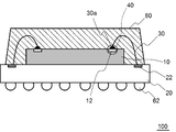
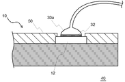
- FIG. 1 is a plan view showing a semiconductor device according to a first embodiment. It is sectional drawing which shows the semiconductor device shown in FIG. It is an enlarged view of the junction part shown in FIG.
- FIG. 7 is a plan view showing a first modification of the semiconductor device shown in FIG. 1.
- FIG. 10 is a cross-sectional view showing a second modification of the semiconductor device shown in FIG. 1.
- FIG. 1 is a plan view showing a semiconductor device 100 according to the present embodiment.
- FIG. 2 is a cross-sectional view showing the semiconductor device 100 shown in FIG.
- the semiconductor device 100 according to this embodiment includes a semiconductor chip 10 and a wire 30.
- the semiconductor chip 10 includes electrode pads 12.
- the wire 30 is electrically connected to the electrode pad 12.
- the wire 30 is made of a first metal material containing Ag as a main component and Pd.
- the electrode pad 12 is made of a second metal material containing Al as a main component.
- An alloy layer containing Ag, Al, and Pd or an alloy layer containing Ag, Al, Pd, and Au is formed at the joint 40 between the wire 30 and the electrode pad 12.
- an alloy layer containing Ag, Al and Pd or an alloy layer containing Ag, Al, Pd and Au is formed.
- the present inventor has found that in such a case, it is possible to realize the joint 40 having an excellent balance of moisture resistance reliability and high-temperature storage characteristics. As a result, the bonding reliability between the wire 30 and the electrode pad 12 can be improved.
- the semiconductor device 100 includes a base material 20 and a semiconductor chip 10 mounted on the base material 20.
- the substrate 20 and the semiconductor chip 10 are electrically connected to each other via a wire 30 (bonding wire).
- a semiconductor device 100 constitutes a semiconductor package in which a semiconductor chip 10 is mounted on a base material 20, for example.
- the semiconductor device 100 according to the present embodiment can include a plurality of semiconductor chips 10 stacked on the base material 20, for example.
- each semiconductor chip 10 is electrically connected to the base material 20 through, for example, a wire 30.
- the base material 20 is not particularly limited as long as it is a member recognized by those skilled in the art as being capable of mounting a semiconductor chip, and is, for example, a wiring board such as an interposer or a mother board, a lead frame, and other semiconductor chips.
- a wiring board such as an interposer or a mother board, a lead frame, and other semiconductor chips.
- FIG. 1 and FIG. 2 the case where the base material 20 is an interposer is illustrated.
- a plurality of solder balls 62 are provided on the other surface of the substrate 20 opposite to the surface on which the semiconductor chip 10 is mounted.
- the semiconductor device 100 including the base material 20 and the semiconductor chip 10 is mounted on another wiring board through, for example, solder balls 62.
- the base material 20 includes connection terminals 22.
- One end of the wire 30 is bonded to the surface portion of the connection terminal 22.
- the connection terminal 22 is provided on one surface of the substrate 20 on which the semiconductor chip 10 is mounted, for example.
- a plurality of connection terminals 22 are provided on one surface of the base material 20.
- the plurality of connection terminals 22 are provided, for example, along the outer edge of the semiconductor chip 10.
- the connection terminal 22 is an electrode pad provided on the base material 20 constituting the interposer.
- connection terminal 22 is made of, for example, a material mainly composed of Au.
- the surface portion of the connection terminal 22 is constituted by a laminated film in which, for example, an Ag or Ni layer, a Pd layer, and an Au layer are laminated in order.
- the semiconductor chip 10 is mounted on the base material 20.
- Examples of the semiconductor chip 10 include an integrated circuit, a large-scale integrated circuit, and a solid-state imaging device.
- the semiconductor chip 10 is bonded onto one surface of the base material 20 via, for example, a film-like or paste-like die attach material.
- the semiconductor chip 10 includes electrode pads 12. The other end of the wire 30 opposite to the end that is bonded to the connection terminal 22 is bonded to the surface portion of the electrode pad 12.
- the electrode pad 12 is provided, for example, on the other surface of the semiconductor chip 10 opposite to the one surface facing the substrate 20. On the other surface of the semiconductor chip 10, for example, a plurality of electrode pads 12 are provided. In this case, the plurality of electrode pads 12 are provided, for example, along the outer edge of the semiconductor chip 10.
- the electrode pad 12 is comprised by the 2nd metal material which has Al as a main component.
- the surface portion of the electrode pad 12 that is bonded to the wire 30 is made of the second metal material.
- the second metal material constituting the electrode pad 12 may contain other metal materials such as Ni, Au, Pd, Ag, Cu, Si, or Pt in addition to Al.
- the content of Al in the second metal material constituting the electrode pad 12 is, for example, 90% by weight or more and 100% by weight or less.
- the wire 30 is electrically connected to the connection terminal 22 and the electrode pad 12.
- one end of the wire 30 is joined to the connection terminal 22, and the other end opposite to the one end is joined to the electrode pad 12.
- a bonding portion 40 formed by bonding them is formed between the tip portion 30a of the wire 30 and the electrode pad 12.
- the semiconductor chip 10 is provided with a plurality of electrode pads 12, and the base material 20 is provided with a plurality of connection terminals 22.
- a plurality of wires 30 are provided to electrically connect each electrode pad 12 and each connection terminal 22 to each other.
- the diameter of the wire 30 is, for example, 15 ⁇ m or more and 25 ⁇ m or less, and particularly preferably 18 ⁇ m or more and 20 ⁇ m or less.
- the wire 30 is made of a first metal material containing Ag as a main component and Pd.
- the tip part 30a joined to the electrode pad 12 in the wire 30 is made of the first metal material.
- the first metal material constituting the wire 30 may contain, for example, Au in addition to Ag and Pd. Thereby, the moisture resistance reliability in the junction part 40 can be improved more effectively.
- the Ag content in the first metal material constituting the wire 30 is preferably 85% by weight or more and 99.5% by weight or less, and more preferably 85% by weight or more and 96% by weight or less. Accordingly, it is possible to improve the moisture resistance reliability and high-temperature storage characteristics at the joint 40 more effectively while reducing the manufacturing cost, and to improve the joint reliability between the wire 30 and the electrode pad 12. Become. Further, the content of Pd in the first metal material constituting the wire 30 is preferably 0.5 wt% or more and 15 wt% or less, more preferably 2 wt% or more and 10 wt% or less, and still more preferably. Is 3% by weight or more and 6% by weight or less.
- the content of Au in the first metal material is, for example, greater than 0% by weight and 10% by weight or less, more preferably 2% by weight or more and 10% by weight. It is as follows. Thereby, the bondability of the wire 30 can be improved. However, when the Ag content is 94% by weight or more, Au does not have to be used.
- FIG. 3 is an enlarged view of the joint 40 shown in FIG.
- a protective film 50 made of, for example, polyimide is formed on the other surface of the semiconductor chip 10.
- the protective film 50 is provided with an opening so that the surface of the electrode pad 12 is exposed.
- the alloy layer 32 containing Ag, Al, and Pd is formed at the joint 40 between the wire 30 and the electrode pad 12. As a result, it is possible to realize the joint 40 having an excellent balance of moisture resistance reliability and high-temperature storage characteristics.
- the alloy layer 32 containing Ag, Al, and Pd has, for example, a composition of the first metal material that constitutes the wire 30, a composition of the second metal material that constitutes the electrode pad 12, and a bonding method of the wire 30 and the electrode pad 12. Each can be formed by appropriately controlling.
- the composition ratio of Ag, Al, and Pd in the alloy layer 32 may be different from each other in each region included in the alloy layer 32, for example.
- the alloy layer 32 in the present embodiment has a higher composition ratio of Ag and Pd and a lower composition ratio of Al, for example, at one end located on the wire 30 side than at the other end located on the electrode pad 12 side. It is provided to become.
- the alloy layer 32 in this embodiment may have the area
- the alloy layer 32 in this embodiment is, for example, one end located on the wire 30 side and the other located on the electrode pad 12 side. It is provided so that the composition ratio of Ag, Pd and Au is higher than that of the end portion, and the composition ratio of Al is lower.
- the wire 30 and the electrode pad 12 are bonded to each other through the alloy layer 32 containing Ag, Al, and Pd, or Ag, Al, Pd, and Au formed in the bonding portion 40.
- the alloy layer 32 is provided in a layer shape or an island shape on the end surface of the wire 30 that is bonded to the electrode pad 12. At this time, the end surface joined to the electrode pad 12 in the wire 30 coincides with the bottom surface of the tip portion 30a.
- the shape of the alloy layer 32 is not limited to this, It can be set as various shapes.
- the semiconductor chip 10 and the wire 30 are sealed with a sealing resin 60 made of, for example, a cured product of an epoxy resin composition.
- a sealing resin 60 made of, for example, a cured product of an epoxy resin composition.
- the joint 40 between the wire 30 and the electrode pad 12 is also sealed with the cured product of the epoxy resin composition.
- the cured product of the epoxy resin composition that seals the semiconductor chip 10 and the wire 30 may contain, for example, an organic sulfur compound.
- an organic sulfur compound In this case, the adhesiveness of the cured product of the epoxy resin composition to the semiconductor chip 10 and the wire 30 composed of the first metal material mainly composed of Ag can be improved. For this reason, the peeling etc. between the sealing resin 60 comprised with the hardened
- the content of sulfur derived from the organic sulfur compound in the cured product of the epoxy resin composition is preferably, for example, from 1 ppm to 400 ppm.
- the sulfur content in the cured product of the epoxy resin composition is the sulfur content derived from the organic sulfur compound.
- the sulfur content is quantified as follows, for example. First, about 5 mg of a cured product of the epoxy resin composition is measured, burned in a flask filled with oxygen, and the generated combustion gas is absorbed in a 5% potassium hydroxide solution. Next, the sulfate ion amount in the 5% potassium hydroxide solution measured by the ion chromatography method is converted into the sulfur content in the epoxy resin composition.
- sulfur content 1 ppm or more the adhesiveness of the hardened
- cured material of an epoxy resin composition can be adjusted by controlling appropriately each component and preparation method which comprise an epoxy resin composition.
- the pH of the cured product of the epoxy resin composition that seals the semiconductor chip 10 and the wire 30 is preferably 4 or more and 7 or less, and more preferably 4.5 or more and 6.5 or less. In this case, it can suppress that the junction part 40 will be corroded by the hardened
- cured material of an epoxy resin composition is adjusted by controlling appropriately each component and preparation method which comprise an epoxy resin composition.
- the epoxy resin composition contains (A) an epoxy resin and (B) a curing agent.
- the (A) epoxy resin contained in the epoxy resin composition monomers, oligomers and polymers generally having two or more epoxy groups in one molecule can be used, and the molecular weight and molecular structure are not particularly limited.
- the (A) epoxy resin may be, for example, a biphenyl type epoxy resin; a bisphenol type epoxy resin such as a bisphenol A type epoxy resin, a bisphenol F type epoxy resin, or a tetramethylbisphenol F type epoxy resin; ; Novolak type epoxy resins such as phenol novolac type epoxy resins and cresol novolak type epoxy resins; Multifunctional epoxy resins such as triphenolmethane type epoxy resins and alkyl-modified triphenolmethane type epoxy resins; Phenol aralkyl type epoxy resins having a phenylene skeleton Aralkyl-type epoxy resins such as phenol aralkyl-type epoxy resins having a biphenylene skeleton; dihydroxy
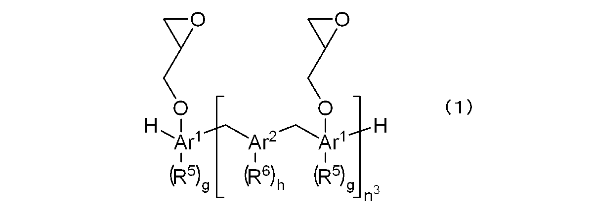
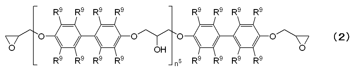
- the epoxy resin (A) is selected from the group consisting of an epoxy resin represented by the following formula (1), an epoxy resin represented by the following formula (2), and an epoxy resin represented by the following formula (3). It is particularly preferable to use a material containing at least one kind.
- Ar 1 represents a phenylene group or a naphthylene group, and when Ar 1 is a naphthylene group, the glycidyl ether group may be bonded to either the ⁇ -position or the ⁇ -position.
- Ar 2 represents any one of a phenylene group, a biphenylene group, and a naphthylene group.
- R 5 and R 6 each independently represents a hydrocarbon group having 1 to 10 carbon atoms.
- g is an integer of 0 to 5
- h is an integer of 0 to 8.
- n 3 represents the degree of polymerization, and the average value is 1 to 3.
- a plurality of R 9s each independently represent a hydrogen atom or a hydrocarbon group having 1 to 4 carbon atoms.
- n 5 represents the degree of polymerization, and the average value is 0-4.
- a plurality of R 10 and R 11 each independently represents a hydrogen atom or a hydrocarbon group having 1 to 4 carbon atoms.
- n 6 represents the degree of polymerization, and the average value is 0-4.
- the content of the epoxy resin is preferably 3% by mass or more, more preferably 5% by mass or more, and further preferably 8% by mass or more with respect to the entire epoxy resin composition. Thereby, wire breakage due to an increase in viscosity of the epoxy resin composition can be suppressed. Moreover, it is preferable that it is 18 mass% or less with respect to the whole epoxy resin composition, as for content of an epoxy resin (A), it is more preferable that it is 13 mass% or less, and 11 mass% or less is further more preferable. Thereby, the fall of moisture-proof reliability by the water absorption rate increase, etc. can be suppressed.
- the (B) curing agent contained in the epoxy resin composition can be roughly classified into three types, for example, a polyaddition type curing agent, a catalyst type curing agent, and a condensation type curing agent.
- polyaddition type curing agents used for curing agents include aliphatic polyamines such as diethylenetriamine (DETA), triethylenetetramine (TETA), and metaxylylenediamine (MXDA), diaminodiphenylmethane (DDM), In addition to aromatic polyamines such as m-phenylenediamine (MPDA) and diaminodiphenylsulfone (DDS), polyamine compounds including dicyandiamide (DICY) and organic acid dihydrazide; hexahydrophthalic anhydride (HHPA), methyltetrahydrophthalic anhydride ( Acid anhydrides including alicyclic acid anhydrides such as MTHPA), trimellitic anhydride (TMA), pyromellitic anhydride (PMDA), benzophenone tetracarboxylic acid (BTDA), etc .; novolac type Phenol resins, phenol resin-based curing agent such as polyvinyl phenol
- Examples of the catalyst-type curing agent used for the curing agent include tertiary amine compounds such as benzyldimethylamine (BDMA) and 2,4,6-trisdimethylaminomethylphenol (DMP-30); 2-methyl Examples thereof include imidazole compounds such as imidazole and 2-ethyl-4-methylimidazole (EMI24); Lewis acids such as BF3 complex.
- BDMA benzyldimethylamine
- DMP-30 2,4,6-trisdimethylaminomethylphenol
- 2-methyl examples thereof include imidazole compounds such as imidazole and 2-ethyl-4-methylimidazole (EMI24); Lewis acids such as BF3 complex.
- condensation type curing agent examples include a resol type phenol resin; a urea resin such as a methylol group-containing urea resin; and a melamine resin such as a methylol group-containing melamine resin.
- a phenol resin-based curing agent is preferable from the viewpoint of improving the balance of flame resistance, moisture resistance, electrical properties, curability, storage stability, and the like.
- the phenol resin-based curing agent monomers, oligomers, and polymers in general having two or more phenolic hydroxyl groups in one molecule can be used, and the molecular weight and molecular structure are not particularly limited.
- novolak-type resin such as a phenol novolak resin, a cresol novolak resin, a bisphenol novolak
- Modified phenolic resins such as terpene modified phenolic resin and dicyclopentadiene modified phenolic resin
- aralkyl type resins such as phenol aralkyl resin having phenylene skeleton and / or biphenylene skeleton, naphthol aralkyl resin having phenylene and / or biphenylene skeleton
- Examples thereof include bisphenol compounds such as bisphenol F, and these may be used alone or in combination of two or more.
- at least one curing agent selected from the group consisting of compounds represented by the following formula (4).
- Ar 3 represents a phenylene group or a naphthylene group.
- Ar 3 represents a naphthylene group
- the hydroxyl group may be bonded to either the ⁇ -position or the ⁇ -position.
- Ar 4 represents any one of a phenylene group, a biphenylene group, and a naphthylene group.
- R 7 and R 8 each independently represents a hydrocarbon group having 1 to 10 carbon atoms.
- i is an integer from 0 to 5
- j is an integer from 0 to 8.
- n 4 represents the degree of polymerization, and the average value is 1 to 3.
- the content of the curing agent is preferably 2% by mass or more, more preferably 3% by mass or more, and further preferably 6% by mass or more with respect to the entire epoxy resin composition. .
- an epoxy resin composition having sufficient fluidity can be obtained.
- curing agent it is more preferable that it is 11 mass% or less, and it is 8 mass% or less. Further preferred. Thereby, the possibility of causing a decrease in moisture resistance reliability due to an increase in water absorption can be reduced.
- the blending ratio of (A) the epoxy resin and (B) the curing agent that is a phenol resin-based curing agent is the number of epoxy groups (EP ) And the phenolic hydroxyl group number (OH) of all phenolic resin-based curing agents, the equivalent ratio (EP) / (OH) is preferably 0.8 or more and 1.3 or less.
- the epoxy resin composition may contain (C) a filler, (D) a neutralizing agent, (E) a curing accelerator, or (F) an organic sulfur compound as necessary.
- (C) Filler As a filler, what is used for the general epoxy resin composition for semiconductor sealing can be used, for example, fused spherical silica, fused crushed silica, crystalline silica, talc, alumina, titanium white, nitriding Examples include inorganic fillers such as silicon, and organic fillers such as organosilicone powder and polyethylene powder. Of these, it is particularly preferable to use fused spherical silica. These fillers may be used alone or in combination of two or more.
- the shape of the filler is preferably as spherical as possible and broad in particle size distribution from the viewpoint of increasing the filler content while suppressing an increase in the melt viscosity of the epoxy resin composition.
- the filler may be surface-treated with a coupling agent.
- the filler (C) may be used after pretreatment with an epoxy resin or a phenol resin.
- a processing method at this time there are a method of removing the solvent after mixing using a solvent, a method of adding directly to the filler, and a mixing process using a mixer.
- the content of the filler is preferably 65% by mass or more, and 75% by mass or more with respect to the entire epoxy resin composition, from the viewpoint of the filling property of the epoxy resin composition and the reliability of the semiconductor device. More preferably, it is more preferably 80% by mass or more. Thereby, low moisture absorption and low thermal expansibility can be improved, and moisture resistance reliability can be made favorable. Further, the content of the filler (C) is preferably 93% by mass or less, more preferably 91% by mass or less, based on the entire epoxy resin composition, from the viewpoint of improving moldability. 86 mass% or less is more preferable. As a result, it is possible to reduce the possibility that the fluidity is lowered and poor filling occurs during molding, or that the inconvenience such as the wire flow in the semiconductor device due to the increase in viscosity occurs.
- (D) Neutralizing agent As a neutralizer, what neutralizes the acidic corrosive gas generated when heating the sealing resin 60 which is an epoxy resin composition or its hardened
- a neutralizing agent As a neutralizing agent, at least 1 sort (s) selected from the group which consists of a basic metal salt, especially the compound containing a calcium element, the compound containing an aluminum element, and the compound containing a magnesium element can be used, for example.
- Examples of the compound containing calcium element used for the neutralizing agent include calcium carbonate, calcium borate, calcium metasilicate, and the like. Among these, calcium carbonate is preferable from the viewpoint of impurity content, water resistance and low water absorption, and precipitated calcium carbonate synthesized by a carbon dioxide reaction method is more preferable.
- Examples of the compound containing an aluminum element used as a neutralizing agent include aluminum hydroxide and boehmite. Among these, aluminum hydroxide is preferable. Moreover, as aluminum hydroxide used for (D) neutralizing agent, the low-soda aluminum hydroxide synthesize
- Hydrotalcite, magnesium oxide, magnesium carbonate, etc. are mentioned as a compound containing the magnesium element used for a neutralizing agent.
- hydrotalcite represented by the following formula (5) from the viewpoint of impurity content and low water absorption.
- M represents a metal element containing at least Mg.
- A, b, and c are numbers satisfying 2 ⁇ a ⁇ 8, 1 ⁇ b ⁇ 3, and 0.5 ⁇ c ⁇ 2, respectively.
- M is an integer of 0 or more.
- (D) a hydrotalcite used in the neutralizing agent for example, Mg 6 Al 2 (OH) 16 (CO 3) ⁇ mH 2 O, Mg 3 ZnAl 2 (OH) 12 (CO 3) ⁇ mH 2 O, Mg 4.3 Al 2 (OH) 12.6 (CO 3 ) ⁇ mH 2 O and the like can be mentioned.
- the moisture absorption can be reduced by setting the content of the (D) neutralizing agent to 10% by mass or less, the solder crack resistance tends to be improved.
- the content thereof is 0.05% by mass or more and 2% by mass or less with respect to the entire epoxy resin composition. More preferably.
- the curing accelerator may be any one that promotes the crosslinking reaction between (A) the epoxy group of the epoxy resin and (B) the curing agent (for example, the phenolic hydroxyl group of the phenol resin-based curing agent), What is used for the general epoxy resin composition for semiconductor sealing can be used.
- Examples of the curing accelerator include phosphorus atom-containing compounds such as organic phosphines, tetra-substituted phosphonium compounds, phosphobetaine compounds, adducts of phosphine compounds and quinone compounds, adducts of phosphonium compounds and silane compounds; Amidines and tertiary amines exemplified by 8-diazabicyclo (5,4,0) undecene-7, benzyldimethylamine, 2-methylimidazole and the like, and nitrogen atom-containing compounds such as amidines and quaternary salts of amines, etc. These may be used alone or in combination of two or more.
- phosphorus atom-containing compounds such as organic phosphines, tetra-substituted phosphonium compounds, phosphobetaine compounds, adducts of phosphine compounds and quinone compounds, adducts of phosphonium compounds and silane compounds
- the content of the curing accelerator is preferably 0.05% by mass or more, and more preferably 0.1% by mass or more with respect to the entire epoxy resin composition. Thereby, it can suppress that sclerosis
- An organic sulfur compound is a compound containing one or more sulfur atoms in one molecule. By containing the organic sulfur compound (F) in the epoxy resin composition, the adhesion of the epoxy resin composition to the semiconductor chip 10 and the wire 30 can be improved.
- organic sulfur compounds include mercaptosilane compounds such as 3-mercaptopropyltrimethoxysilane, mercapto compounds having a triazole skeleton such as 3-amino-5-mercapto-1,2,4-triazole, trans- Dithian compounds such as 4,5-dihydroxy-1,2-dithiane, 2- (methylthio) -2-thiazoline compounds, benzothiazole compounds such as 2-mercaptobenzothiazole, 2-mercaptoethanol, 3-mercapto-1 , 2-propanediol and other mercapto group-containing alcohols. These may be used alone or in combination of two or more.
- a mercaptosilane compound such as 3-mercaptopropyltrimethoxysilane as the (F) organic sulfur compound.
- a mercaptosilane compound such as 3-mercaptopropyltrimethoxysilane also functions as a coupling agent.
- the content of the organic sulfur compound is preferably 0.05% by mass or more and 1% by mass or less, and preferably 0.1% by mass or more and 0.5% by mass or less with respect to the entire epoxy resin composition. Particularly preferred. Thereby, in order to implement
- the epoxy resin composition constituting the sealing resin 60 may further include an aluminum corrosion inhibitor such as zirconium hydroxide; an inorganic ion exchanger such as bismuth oxide hydrate; and ⁇ -glycidoxypropyltrimethoxy as necessary.
- Coupling agents such as silane, 3-aminopropyltrimethoxysilane, and epoxy silane; Colorants such as carbon black and bengara; Low stress components such as silicone rubber; Natural wax such as carnauba wax; Synthetic wax; Zinc stearate Release agents such as higher fatty acids and their metal salts or paraffin; flame retardants such as aluminum hydroxide, magnesium hydroxide, zinc borate, zinc molybdate, phosphazene, and various additives such as antioxidants may be appropriately blended Good.
- the above-mentioned components are mixed at 15 ° C. to 28 ° C. using a mixer or the like, and further melted in a kneader such as a roll, kneader or extruder What knead
- pulverized can use what adjusted dispersity, fluidity
- FIG. 4 is a plan view showing a first modification of the semiconductor device 100 shown in FIG.
- the base material 20 is a lead frame including a die pad 24 on which the semiconductor chip 10 is mounted and an inner lead.
- the connection terminal 22 provided in the base material 20 is comprised by an inner lead, for example.
- the bonding wire 30 connects the electrode 12 provided on the semiconductor chip 10 and the connection terminal 22 constituted by the inner lead to each other.
- the base material 20 is comprised by Cu alloy or 42 alloy, for example.
- the surface portion of the connection terminal 22 is constituted by a laminated film in which, for example, an Ag or Ni layer, a Pd layer, and an Au layer are laminated in order. In this case, it is possible to realize high bonding reliability between the bonding wire 30 and the connection terminal 22.
- FIG. 5 is a cross-sectional view showing a second modification of semiconductor device 100 shown in FIG.
- a plurality of semiconductor chips 10 are stacked on the base material 20.
- Any two semiconductor chips 10 among the plurality of semiconductor chips 10 are electrically connected to each other by, for example, wires 34. That is, the wire 34 is connected to the electrode pad 12 of one semiconductor chip 10 and the electrode pad 12 of another semiconductor chip 10.
- the wire 34 can have the same configuration as the wire 30, for example.
- An alloy layer containing Ag, Al, and Pd is formed at the joint between the wire 34 and the electrode pad 12.
- the alloy layer provided at the joint between the wire 34 and the electrode pad 12 has the same configuration as the alloy layer 32 provided at the joint between the wire 30 and the electrode pad 12 described above.
- FIG. 5 illustrates a case where two semiconductor chips 10 are stacked on the base material 20. Note that the configuration of the semiconductor device 100 according to the present modification is not limited to that shown in FIG. In this modification, for example, an arbitrary number of semiconductor chips 10 can be stacked on the base material 20.
- the semiconductor chip 10 provided with the electrode pad 12 is prepared.
- the semiconductor chip 10 is obtained, for example, by forming a multilayer wiring layer on a wafer on which elements such as transistors are formed, and then dicing the wafer into individual semiconductor chips 10.
- the semiconductor chip 10 is mounted on the base material 20 including the connection terminals 22.
- the semiconductor chip 10 is disposed on a region of the base material 20 where the connection terminals 22 are not provided.
- the semiconductor chip 10 is mounted on the base material 20 via, for example, a die attach material provided on the base material 20.
- the electrode pads 12 of the semiconductor chip 10 and the connection terminals 22 of the base material 20 are wire-bonded with the wires 30. Thereby, the electrode pad 12 and the connection terminal 22 are electrically connected.
- the wire bonding is performed in an inert gas atmosphere such as nitrogen, argon, or helium, based on the general condition that a person skilled in the art performs wire bonding using an Au wire, for example.
- the bonding apparatus for example, a bonding apparatus for Cu wire can be used.
- the semiconductor chip 10 and the wire 30 are sealed with an epoxy resin composition.
- the epoxy resin composition is cured and molded using a molding method such as a transfer mold, a compression mold, or an injection mold.
- the epoxy resin composition is post-cured at a temperature of about 80 ° C. to 200 ° C. for about 10 minutes to 24 hours.
- the sealing resin 60 comprised with the hardened
- the post-curing is particularly preferably performed under conditions of 150 to 200 ° C. and 2 to 16 hours. According to the present embodiment, for example, the semiconductor device 100 is formed in this way.
- the wire 30 made of the first metal material containing Ag as the main component and containing Pd, and the electrode pad 12 made of the second metal material containing Al as the main component.
- An alloy layer containing Ag, Al, and Pd is formed at the joint 40. Thereby, it is possible to improve the bonding reliability between the wire and the electrode pad.
- an epoxy resin composition was prepared as follows. First, each component blended according to Table 1 was mixed at 15 to 28 ° C. using a mixer. Next, the obtained mixture was roll kneaded at 70 to 100 ° C. Next, the kneaded mixture was cooled and pulverized to obtain an epoxy resin composition.
- the details of each component in Table 1 are as follows. Moreover, the unit in Table 1 is mass%.
- the cured products of the epoxy resin compositions of Production Examples 1 to 3 were subjected to a low-pressure transfer molding machine (“KTS-15” manufactured by Kotaki Seiki Co., Ltd.) under conditions of a mold temperature of 175 ° C., an injection pressure of 7.5 MPa, and a curing time of 2 minutes. ”) To obtain a 50 mm ⁇ ⁇ 3 mm test piece. Subsequently, the obtained test piece was post-cured under conditions of 175 ° C. for 4 hours and then finely pulverized to obtain a pulverized product.
- KTS-15 low-pressure transfer molding machine
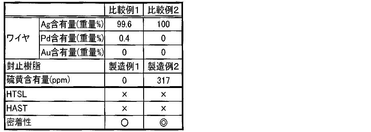
- Examples 1 to 7 and Comparative Examples 1 and 2 semiconductor devices were fabricated as follows.
- a TEG (Test Element Group) chip (3.5 mm ⁇ 3.5 mm) having an electrode pad made of a metal material having an Al purity of 95.0% (Cu 5.0%) is replaced with a 352-pin BGA (the substrate has a thickness of 0). .56 mm, bismaleimide / triazine resin / glass cloth substrate, package size 30 mm ⁇ 30 mm, thickness 1.17 mm).
- connection terminals a wire composed of a metal material according to Tables 2 and 3 for the electrode pads of the TEG chip (hereinafter referred to as electrode pads) and the connection terminals (hereinafter referred to as connection terminals) of the BGA substrate.
- the structure thus obtained is in accordance with Tables 2 and 3 using a low-pressure transfer molding machine (“Y series” manufactured by TOWA) under conditions of a mold temperature of 175 ° C., an injection pressure of 6.9 MPa, and a curing time of 2 minutes. Sealing molding was performed using the epoxy resin composition obtained in the production example, and a 352-pin BGA package was produced. Thereafter, the obtained BGA package was post-cured at 175 ° C. for 4 hours to obtain a semiconductor device.
- Y series low-pressure transfer molding machine
- HAST saturated moisture resistance test
- HTSL High Temperature Storage Test
- the semiconductor devices of Examples 1 to 7 and Comparative Examples 1 and 2 were subjected to HTSL (High Temperature Storage Test).
- HTSL was performed under test conditions of a temperature of 185 ° C. and 1000 hours.
- the electrical resistance value between the wire and the electrode pad is measured, and the electrical resistance value less than 110% of the initial resistance value is ⁇ , and the electrical resistance value is 110% or more and 120% or less. What is shown is ⁇ , and what shows an electric resistance value greater than 120% is ⁇ .
- Examples 1 to 7 an alloy layer containing Ag, Al, and Pd was observed at the joint between the wire and the electrode pad.
- good results were obtained in all of the high-temperature storage characteristics, the moisture resistance reliability test, and the adhesion.
- semiconductor devices having particularly excellent adhesion as compared with the other examples were obtained.
- Examples 1 to 6 a semiconductor device having particularly excellent high-temperature storage characteristics as compared with Example 7 was obtained.
- semiconductor devices that were particularly excellent in moisture resistance reliability were obtained as compared with other Examples.
Landscapes
- Structures Or Materials For Encapsulating Or Coating Semiconductor Devices Or Solid State Devices (AREA)
- Wire Bonding (AREA)
Abstract
Description
前記電極パッドに電気的に接続されたワイヤと、
を備え、
前記ワイヤは、Agを主成分としてPdを含む第1金属材料により構成されており、
前記電極パッドは、Alを主成分とする第2金属材料により構成されており、
前記ワイヤと前記電極パッドとの接合部には、Ag、AlおよびPdを含む合金層が形成されている半導体装置が提供される。
本実施形態に係る半導体装置100は、半導体チップ10と、ワイヤ30と、を備えている。半導体チップ10は、電極パッド12を備えている。ワイヤ30は、電極パッド12に電気的に接続されている。ワイヤ30は、Agを主成分としてPdを含む第1金属材料により構成されている。電極パッド12は、Alを主成分とする第2金属材料により構成されている。ワイヤ30と電極パッド12との接合部40には、Ag、AlおよびPdを含む合金層、またはAg、Al、PdおよびAuを含む合金層が形成されている。
図1に示す例では、基材20上に一の半導体チップ10が搭載されている場合が示されている。一方で、本実施形態に係る半導体装置100は、たとえば基材20上に互いに積層された複数の半導体チップ10を備えることもできる。この場合、各半導体チップ10は、たとえばそれぞれワイヤ30を介して基材20に電気的に接続される。
図1および図2においては、基材20がインターポーザである場合が例示されている。この場合、基材20のうち半導体チップ10を搭載する一面と反対の他面には、複数の半田ボール62が設けられる。基材20および半導体チップ10を備える半導体装置100は、たとえば半田ボール62を介して他の配線基板上に搭載される。
接続端子22は、たとえば基材20のうちの半導体チップ10を搭載する一面上に設けられている。基材20の一面上には、たとえば複数の接続端子22が設けられる。この場合、複数の接続端子22は、たとえば半導体チップ10の外縁に沿って設けられる。図1に示す例において、接続端子22は、インターポーザを構成する基材20上に設けられた電極パッドである。
また、基材20がリードフレームである場合には、接続端子22の表面部分は、たとえばAgまたはNi層、Pd層、およびAu層が順に積層された積層膜により構成される。
電極パッド12は、たとえば半導体チップ10のうち基材20と対向する一面と反対側の他面上に設けられている。半導体チップ10の他面上には、たとえば複数の電極パッド12が設けられる。この場合、複数の電極パッド12は、たとえば半導体チップ10の外縁に沿って設けられる。
本実施形態において、電極パッド12を構成する第2金属材料中におけるAlの含有量は、たとえば90重量%以上100重量%以下である。
本実施形態において、ワイヤ30の径は、たとえば15μm以上25μm以下であり、とくに好ましくは18μm以上20μm以下である。
また、ワイヤ30を構成する第1金属材料中におけるPdの含有量は、好ましくは0.5重量%以上15重量%以下であり、より好ましくは2重量%以上10重量%以下であり、さらに好ましくは3重量%以上6重量%以下である。これにより、製造コストの増大を抑えつつ、耐湿信頼性や高温保管特性をより効果的に向上させることが可能となる。また、第1金属材料中にAuが含まれる場合、第1金属材料中におけるAuの含有量は、たとえば0重量%よりも大きく、かつ10重量%以下、より好ましくは2重量%以上10重量%以下である。これにより、ワイヤ30のボンディング性を向上させることが可能となる。ただし、Ag含有量が94重量%以上の場合はAuは使用しなくとも差し支えない。
合金層32内におけるAg、AlおよびPdの組成比は、たとえば合金層32内に含まれる各領域において互いに異なっていてもよい。本実施形態における合金層32は、たとえばワイヤ30側に位置する一端部において、電極パッド12側に位置する他端部よりも、AgおよびPdの組成比が高くなり、かつAlの組成比が低くなるように設けられる。なお、本実施形態における合金層32は、電極パッド12側に位置する他端部においてPdを含まない領域を有していてもよいが、当該領域を有しないことが好ましい。
また、ワイヤ30を構成する第1金属材料中にAuが含まれている場合、本実施形態における合金層32は、たとえば前記ワイヤ30側に位置する一端部において、電極パッド12側に位置する他端部よりも、Ag、PdおよびAuの組成比が高くなり、かつAlの組成比が低くなるように設けられる。
図3に示す例において、合金層32は、ワイヤ30のうち電極パッド12に接合される端面において層状または島状に設けられている。このとき、ワイヤ30のうち電極パッド12に接合される端面とは、先端部30aの底面に一致する。なお、合金層32の形状はこれに限定されず、種々の形状とすることができる。
エポキシ樹脂組成物の硬化物中における有機硫黄化合物に由来する硫黄の含有量は、たとえば1ppm以上400ppm以下であることが好ましい。ここでは、エポキシ樹脂組成物の硬化物中における硫黄含有量を、有機硫黄化合物に由来する硫黄の含有量としている。硫黄含有量は、たとえば以下のようにして定量される。まず、エポキシ樹脂組成物の硬化物を約5mg測りとり、内部を酸素で満たしたフラスコ内において燃焼させ、発生した燃焼ガスを5%水酸化カリウム溶液に吸収させる。次に、イオンクロマトグラフ法により測定した5%水酸化カリウム溶液中の硫酸イオン量を、エポキシ樹脂組成物中における硫黄含有量に換算する。
硫黄含有量を1ppm以上とすることにより、ワイヤ30や半導体チップ10に対する上記エポキシ樹脂組成物の硬化物の密着性を効果的に向上させることができる。また、硫黄含有量を400ppm以下とすることにより、エポキシ樹脂組成物の硬化物により封止される接合部40における高温保管特性を向上させることが可能となる。なお、エポキシ樹脂組成物の硬化物中における硫黄含有量は、エポキシ樹脂組成物を構成する成分や調製方法をそれぞれ適切に制御することにより調整することが可能である。
なお、エポキシ樹脂組成物の硬化物のpHは、エポキシ樹脂組成物を構成する成分や調製方法をそれぞれ適切に制御することにより調整される。
エポキシ樹脂組成物に含まれる(A)エポキシ樹脂としては、1分子内にエポキシ基を2個以上有するモノマー、オリゴマー、ポリマー全般を用いることができ、その分子量や分子構造は特に限定されない。
本実施形態において、(A)エポキシ樹脂としては、例えば、ビフェニル型エポキシ樹脂;ビスフェノールA型エポキシ樹脂、ビスフェノールF型エポキシ樹脂、テトラメチルビスフェノールF型エポキシ樹脂等のビスフェノール型エポキシ樹脂;スチルベン型エポキシ樹脂;フェノールノボラック型エポキシ樹脂、クレゾールノボラック型エポキシ樹脂等のノボラック型エポキシ樹脂;トリフェノールメタン型エポキシ樹脂、アルキル変性トリフェノールメタン型エポキシ樹脂等の多官能エポキシ樹脂;フェニレン骨格を有するフェノールアラルキル型エポキシ樹脂、ビフェニレン骨格を有するフェノールアラルキル型エポキシ樹脂等のアラルキル型エポキシ樹脂;ジヒドロキシナフタレン型エポキシ樹脂、ジヒドロキシナフタレンの2量体をグリシジルエーテル化して得られるエポキシ樹脂等のナフトール型エポキシ樹脂;トリグリシジルイソシアヌレート、モノアリルジグリシジルイソシアヌレート等のトリアジン核含有エポキシ樹脂;ジシクロペンタジエン変性フェノール型エポキシ樹脂等の有橋環状炭化水素化合物変性フェノール型エポキシ樹脂が挙げられ、これらは1種類を単独で用いても2種類以上を併用してもよい。これらのうち、ビフェニル型エポキシ樹脂、ビスフェノールA型エポキシ樹脂、ビスフェノールF型エポキシ樹脂、およびテトラメチルビスフェノールF型エポキシ樹脂等のビスフェノール型エポキシ樹脂、ならびにスチルベン型エポキシ樹脂は結晶性を有するものが好ましい。

エポキシ樹脂組成物に含まれる(B)硬化剤としては、たとえば重付加型の硬化剤、触媒型の硬化剤、および縮合型の硬化剤の3タイプに大別することができる。
(B)硬化剤に用いられるフェノール樹脂系硬化剤としては、たとえばフェノールノボラック樹脂、クレゾールノボラック樹脂、ビスフェノールノボラック等のノボラック型樹脂;ポリビニルフェノール;トリフェノールメタン型フェノール樹脂等の多官能型フェノール樹脂;テルペン変性フェノール樹脂、ジシクロペンタジエン変性フェノール樹脂等の変性フェノール樹脂;フェニレン骨格及び/又はビフェニレン骨格を有するフェノールアラルキル樹脂、フェニレン及び/又はビフェニレン骨格を有するナフトールアラルキル樹脂等のアラルキル型樹脂;ビスフェノールA、ビスフェノールF等のビスフェノール化合物等が挙げられ、これらは1種類を単独で用いても2種類以上を併用してもよい。

(C)充填材としては、一般の半導体封止用エポキシ樹脂組成物に使用されているものを用いることができ、たとえば溶融球状シリカ、溶融破砕シリカ、結晶シリカ、タルク、アルミナ、チタンホワイト、窒化珪素等の無機充填材、オルガノシリコーンパウダー、ポリエチレンパウダー等の有機充填材が挙げられる。これらのうち、溶融球状シリカを用いることがとくに好ましい。これらの充填材は、1種を単独で用いても2種以上を併用しても差し支えない。
(D)中和剤としては、エポキシ樹脂組成物、またはその硬化物である封止樹脂60を加熱する際に発生する酸性の腐食性ガスを中和するものを用いることができる。これにより、ワイヤ30と半導体チップ10の電極パッド12との接合部40の腐食(酸化劣化)を抑制することができる。(D)中和剤としては、たとえば塩基性金属塩、特にカルシウム元素を含む化合物、アルミニウム元素を含む化合物およびマグネシウム元素を含む化合物からなる群から選択される少なくとも1種を用いることができる。
MaAlb(OH)2a+3b-2c(CO3)c・mH2O (5)
(式(5)中、Mは少なくともMgを含む金属元素を表す。a、b、cは、それぞれ2≦a≦8、1≦b≦3、0.5≦c≦2を満たす数であり、mは0以上の整数である。)
(E)硬化促進剤は、(A)エポキシ樹脂のエポキシ基と、(B)硬化剤(たとえば、フェノール樹脂系硬化剤のフェノール性水酸基)と、の架橋反応を促進させるものであればよく、一般の半導体封止用エポキシ樹脂組成物に使用するものを用いることができる。(E)硬化促進剤としては、たとえば有機ホスフィン、テトラ置換ホスホニウム化合物、ホスホベタイン化合物、ホスフィン化合物とキノン化合物との付加物、ホスホニウム化合物とシラン化合物との付加物等のリン原子含有化合物;1,8-ジアザビシクロ(5,4,0)ウンデセン-7、ベンジルジメチルアミン、2-メチルイミダゾール等が例示されるアミジンや3級アミン、さらには前記アミジン、アミンの4級塩等の窒素原子含有化合物等が挙げられ、これらは1種類を単独で用いても2種以上を併用しても差し支えない。
(F)有機硫黄化合物は、1分子中に硫黄原子を1以上含有する化合物である。エポキシ樹脂組成物に(F)有機硫黄化合物を含有させることにより、半導体チップ10およびワイヤ30に対するエポキシ樹脂組成物の密着性を向上させることができる。(F)有機硫黄化合物としては、たとえば3-メルカプトプロピルトリメトキシシラン等のメルカプトシラン化合物、または3-アミノ-5-メルカプト-1,2,4-トリアゾール等のトリアゾール骨格を有するメルカプト化合物、トランス-4,5-ジヒドロキシ-1,2-ジチアン等のジチアン系化合物、2-(メチルチオ)-2-チアゾリン系化合物、2-メルカプトベンゾチアゾール等のベンゾチアゾール系化合物、2-メルカプトエタノール、3-メルカプトー1,2-プロパンジオールなどのメルカプト基含有アルコールが挙げられこれらは1種類を単独で用いても2種以上を併用しても差し支えない。
これらの中でも、3-メルカプトプロピルトリメトキシシラン等のメルカプトシラン化合物を(F)有機硫黄化合物として用いることがとくに好ましい。これにより、半導体チップ10やワイヤ30に対する密着性および高温保管特性のバランスに優れたエポキシ樹脂組成物を実現できる。なお、3-メルカプトプロピルトリメトキシシラン等のメルカプトシラン化合物は、カップリング剤としても機能する。
本変形例において、基材20は、半導体チップ10を搭載するダイパッド24と、インナーリードと、を含むリードフレームである。この場合、基材20に設けられる接続端子22は、たとえばインナーリードにより構成される。このため、ボンディングワイヤ30は、半導体チップ10に設けられた電極12と、インナーリードにより構成される接続端子22と、を互いに接続することとなる。
本実施形態において、基材20は、たとえばCu合金または42アロイにより構成される。また、接続端子22について、その表面部分は、たとえばAgまたはNi層、Pd層、Au層が順に積層された積層膜により構成される。この場合、ボンディングワイヤ30と接続端子22との間において高い接合信頼性を実現することが可能となる。
本変形例において、基材20上には、複数の半導体チップ10が互いに積層される。複数の半導体チップ10のうち任意の二つの半導体チップ10の間は、たとえばワイヤ34により互いに電気的に接続される。すなわち、ワイヤ34は、一の半導体チップ10の電極パッド12と、他の半導体チップ10の電極パッド12と、に対して接続されることとなる。ワイヤ34は、たとえばワイヤ30と同様の構成を有することができる。
ワイヤ34と電極パッド12との接合部には、Ag、AlおよびPdを含む合金層が形成される。ワイヤ34と電極パッド12との接合部に設けられる合金層は、上述したワイヤ30と電極パッド12との接合部に設けられる合金層32と同様の構成を有する。この場合、互いに積層される二つの半導体チップ10を接続するワイヤ34と、ワイヤ34に接続される電極パッド12と、の間においても、耐湿信頼性および高温保管特性等のバランスに優れた接合部を実現することが可能となる。
図5においては、基材20上に、二つの半導体チップ10が積層される場合が例示されている。なお、本変形例に係る半導体装置100の構成は、図5に示すものに限定されない。本変形例においては、たとえば任意の数の半導体チップ10を基材20上に積層することが可能である。
まず、電極パッド12を備える半導体チップ10を準備する。半導体チップ10は、たとえばトランジスタ等の素子が形成されたウェハ上に多層配線層を形成した後、当該ウェハをダイシングして各半導体チップ10に個片化することにより得られる。
次いで、接続端子22を備える基材20上に、半導体チップ10を搭載する。ここでは、基材20のうち接続端子22が設けられていない領域上に半導体チップ10が配置される。本実施形態においては、たとえば基材20上に設けられたダイアタッチ材を介して、基材20上に半導体チップ10を搭載する。
次いで、エポキシ樹脂組成物に対し、80℃~200℃程度の温度で、10分~24時間程度の時間をかけて後硬化を行う。これにより、エポキシ樹脂組成物の硬化物により構成される封止樹脂60が形成される。上記後硬化は、150℃~200℃、2~16時間の条件下により行うことがとくに好ましい。
本実施形態によれば、たとえばこのようにして半導体装置100が形成される。
製造例1~3のそれぞれについて、以下のようにエポキシ樹脂組成物を調整した。
まず、表1に従い配合された各成分を、ミキサーを用いて15~28℃で混合した。次いで、得られた混合物を、70~100℃でロール混練した。次いで、混練後の混合物を冷却し、粉砕してエポキシ樹脂組成物を得た。なお、表1中における各成分の詳細は下記のとおりである。また、表1中の単位は、質量%である。
EP-BA(ビフェニレン骨格を有するフェノールアラルキル型エポキシ樹脂):NC3000P、日本化薬(株)製、エポキシ当量276、Clイオン濃度280ppm
(B)硬化剤
HD-BA(ビフェニレン骨格を有するフェノールアラルキル樹脂):MEH-7851SS、明和化成(株)製、水酸基当量203
(C)充填材
シリカ:FB-820、電気化学工業(株)製、平均粒径26.5μm、105μm以上の粒子1%以下
(D)中和剤
ハイドロタルサイト:DHT-4A(登録商標)(上記式(5)において、aが4.3であり、bが2であり、cが1であるハイドロタルサイト)協和化学工業(株)製
(E)硬化促進剤
トリフェニルホスフィン(TPP)、北興化学工業(株)製
(F)有機硫黄化合物
化合物1:3-メルカプトプロピルトリメトキシシラン
化合物2:3-アミノ-5-メルカプト-1,2,4-トリアゾール
(G)その他の成分
カップリング剤:エポキシシラン
着色剤:カーボンブラック
離型剤:カルナバワックス
低圧トランスファー成形機(コータキ精機(株)製「KTS-15」)を用いて、EMMI-1-66に準じたスパイラルフロー測定用の金型に、金型温度175℃、注入圧力6.9MPa、硬化時間120秒の条件で、製造例1~3のエポキシ樹脂組成物をそれぞれ注入し、流動長を測定した。表1における単位はcmである。
175℃に加熱した熱板上で製造例1~3のエポキシ樹脂組成物をそれぞれ溶融した後、へらで練りながら硬化するまでの時間を測定した。表1における単位は秒である。
製造例1~3のエポキシ樹脂組成物の硬化物を、金型温度175℃、注入圧力7.5MPa、硬化時間2分の条件下で低圧トランスファー成形機(コータキ精機(株)製「KTS-15」)を用いて成形し、50mmφ×3mmの試験片を得た。次いで、得られた試験片を175℃4時間の条件下で後硬化した後に微粉砕して、粉砕品を得た。次いで、5gの粉砕品に50mlの蒸留水を加え、テフロン(登録商標)ライニングした容器に入れ、125℃20時間の処理を行い、抽出液を得た。pHメータを使用し抽出液のpHを測定した。
製造例1~3のエポキシ樹脂組成物の硬化物を約5mg測りとり、内部を酸素で満たしたフラスコ内において燃焼させた。これにより発生した燃焼ガスを5%水酸化カリウム溶液に吸収させた。イオンクロマトグラフ法により測定した5%水酸化カリウム溶液中の硫酸イオン量から、エポキシ樹脂組成物中における硫黄含有量に換算した。表1における単位はppmである。

実施例1~7、比較例1~2のそれぞれについて、以下のように半導体装置を作製した。
Al純度95.0%(Cu5.0%)の金属材料により構成される電極パッドを備えるTEG(Test Element Group)チップ(3.5mm×3.5mm)を、352ピンBGA(基板は厚さ0.56mm、ビスマレイミド・トリアジン樹脂/ガラスクロス基板、パッケージサイズは30mm×30mm、厚さ1.17mm)上に搭載した。次いで、TEGチップの電極パッド(以下、電極パッド)と、BGA基板の接続端子(以下、接続端子)と、を表2および3に従う金属材料により構成されるワイヤを用いてワイヤピッチ80μmでワイヤボンディングした。
これにより得られた構造体を、低圧トランスファー成形機(TOWA製「Yシリーズ」)を用いて、金型温度175℃、注入圧力6.9MPa、硬化時間2分の条件で、表2および3に従う製造例により得られたエポキシ樹脂組成物を用いて封止成形し、352ピンBGAパッケージを作製した。その後、得られたBGAパッケージを175℃、4時間の条件で後硬化し、半導体装置を得た。
実施例1~7、比較例1~2のそれぞれについて、得られた半導体装置を175℃、16時間、大気中の条件下において加熱した後、ワイヤと電極パッドとの接合部の構造を、透過型電子顕微鏡(TEM)を用いて解析した。
実施例1~7の半導体装置では、ワイヤと電極パッドとの接合部においてAg、AlおよびPdを含む合金層が観察された。一方で、比較例1~2の半導体装置では、ワイヤと電極パッドとの接合部においてAg、AlおよびPdを含む合金層は観察されなかった。
実施例1~7、比較例1~2の半導体装置について、HAST(不飽和耐湿性試験)を行った。HASTは、IEC68-2-66に準拠して、温度130℃、湿度85%RH、印加電圧20V、96時間の試験条件下において行った。試験後の半導体装置についてワイヤと電極パッドとの間における電気抵抗値を測定し、初期抵抗値に対し110%未満の電気抵抗値を示すものを◎、110%以上120%以下の電気抵抗値を示すものを○、120%よりも大きい電気抵抗値を示すものを×とした。
実施例1~7、比較例1~2の半導体装置について、HTSL(高温保管試験)を行った。HTSLは、温度185℃、1000時間の試験条件下において行った。試験後の半導体装置についてワイヤと電極パッドとの間における電気抵抗値を測定し、初期抵抗値に対し110%未満の電気抵抗値を示すものを◎、110%以上120%以下の電気抵抗値を示すものを○、120%よりも大きい電気抵抗値を示すものを×とした。
実施例1~7、比較例1~2のそれぞれについて、得られた半導体装置4個に対し85℃相対湿度85%の環境下で168時間処理した後、IRリフロー処理(260℃)を行った。次いで、処理後の半導体装置内部を超音波探傷装置で観察し、封止樹脂が半導体チップまたはワイヤから剥離した剥離面積を算出した。全ての半導体装置について剥離面積が5%未満の場合を◎、5%以上10%以下の場合を○、10%を超える場合を×とした。

Claims (5)
- 電極パッドを備える半導体チップと、
前記電極パッドに電気的に接続されたワイヤと、
を備え、
前記ワイヤは、Agを主成分としてPdを含む第1金属材料により構成されており、
前記電極パッドは、Alを主成分とする第2金属材料により構成されており、
前記ワイヤと前記電極パッドとの接合部には、Ag、AlおよびPdを含む合金層が形成されている半導体装置。 - 請求項1に記載の半導体装置において、
前記ワイヤを構成する前記第1金属材料中におけるAgの含有量は、85重量%以上99.5重量%以下である半導体装置。 - 請求項1または2に記載の半導体装置において、
前記半導体チップおよび前記ワイヤは、エポキシ樹脂組成物の硬化物により封止されており、
前記エポキシ樹脂組成物の硬化物中における硫黄の含有量は、1ppm以上400ppm以下である半導体装置。 - 請求項3に記載の半導体装置において、
前記エポキシ樹脂組成物の硬化物は、有機硫黄化合物を含む半導体装置。 - 請求項3または4に記載の半導体装置において、
前記エポキシ樹脂組成物の硬化物のpHは、4以上7以下である半導体装置。
Priority Applications (3)
| Application Number | Priority Date | Filing Date | Title |
|---|---|---|---|
| JP2015522807A JP6341203B2 (ja) | 2013-06-20 | 2014-06-11 | 半導体装置 |
| CN201480034970.1A CN105308731B (zh) | 2013-06-20 | 2014-06-11 | 半导体装置 |
| KR1020167000689A KR102215169B1 (ko) | 2013-06-20 | 2014-06-11 | 반도체 장치 |
Applications Claiming Priority (2)
| Application Number | Priority Date | Filing Date | Title |
|---|---|---|---|
| JP2013-129375 | 2013-06-20 | ||
| JP2013129375 | 2013-06-20 |
Publications (1)
| Publication Number | Publication Date |
|---|---|
| WO2014203777A1 true WO2014203777A1 (ja) | 2014-12-24 |
Family
ID=52104514
Family Applications (1)
| Application Number | Title | Priority Date | Filing Date |
|---|---|---|---|
| PCT/JP2014/065429 Ceased WO2014203777A1 (ja) | 2013-06-20 | 2014-06-11 | 半導体装置 |
Country Status (5)
| Country | Link |
|---|---|
| JP (1) | JP6341203B2 (ja) |
| KR (1) | KR102215169B1 (ja) |
| CN (1) | CN105308731B (ja) |
| TW (1) | TWI611532B (ja) |
| WO (1) | WO2014203777A1 (ja) |
Cited By (2)
| Publication number | Priority date | Publication date | Assignee | Title |
|---|---|---|---|---|
| JP2017037924A (ja) * | 2015-08-07 | 2017-02-16 | 株式会社ジェイデバイス | 半導体パッケージ |
| JP2017179185A (ja) * | 2016-03-31 | 2017-10-05 | 住友ベークライト株式会社 | 半導体封止用エポキシ樹脂組成物および半導体装置 |
Families Citing this family (1)
| Publication number | Priority date | Publication date | Assignee | Title |
|---|---|---|---|---|
| JP7146719B2 (ja) * | 2019-10-31 | 2022-10-04 | タツタ電線株式会社 | 半導体装置 |
Citations (3)
| Publication number | Priority date | Publication date | Assignee | Title |
|---|---|---|---|---|
| JP2009152561A (ja) * | 2007-11-29 | 2009-07-09 | Sumitomo Bakelite Co Ltd | 半導体装置並びに封止用エポキシ樹脂組成物及びその製造方法 |
| JP2010114408A (ja) * | 2008-10-10 | 2010-05-20 | Sumitomo Bakelite Co Ltd | 半導体装置 |
| WO2012108082A1 (ja) * | 2011-02-10 | 2012-08-16 | 田中電子工業株式会社 | Ag-Au-Pd三元合金系ボンディングワイヤ |
Family Cites Families (10)
| Publication number | Priority date | Publication date | Assignee | Title |
|---|---|---|---|---|
| JP2001176912A (ja) | 1999-12-16 | 2001-06-29 | Noge Denki Kogyo:Kk | 金被覆した銀線ボンディングワイヤ |
| JP2001196411A (ja) | 2000-01-11 | 2001-07-19 | Noge Denki Kogyo:Kk | 金被覆した銀線ボンディングワイヤ |
| JP4596467B2 (ja) * | 2005-06-14 | 2010-12-08 | 田中電子工業株式会社 | 高い接合信頼性、圧着ボールの高い真円性、高い直進性および高い耐樹脂流れ性を有するボンディングワイヤ用金合金線 |
| JP2008166314A (ja) * | 2006-12-26 | 2008-07-17 | Sumitomo Bakelite Co Ltd | 半導体装置及び封止用エポキシ樹脂組成物 |
| JP2008174779A (ja) | 2007-01-17 | 2008-07-31 | Tanaka Electronics Ind Co Ltd | ワイヤ材料およびその製造方法 |
| JP2008251635A (ja) * | 2007-03-29 | 2008-10-16 | Tanaka Electronics Ind Co Ltd | 高い接合信頼性および圧着ボールの高い真円性を有し、さらにAlパッドとその下部が損傷しにくくかつ一層高い耐樹脂流れ性を有するボンディングワイヤ用金合金線 |
| CN103295992A (zh) * | 2008-10-10 | 2013-09-11 | 住友电木株式会社 | 半导体装置 |
| JP4886899B2 (ja) | 2009-03-17 | 2012-02-29 | 新日鉄マテリアルズ株式会社 | 半導体用ボンディングワイヤ |
| US8101123B2 (en) * | 2009-03-23 | 2012-01-24 | Lee Jun-Der | Composite alloy bonding wire and manufacturing method thereof |
| JP5616165B2 (ja) * | 2010-08-24 | 2014-10-29 | タツタ電線株式会社 | 銀ボンディングワイヤ |
-
2014
- 2014-06-11 WO PCT/JP2014/065429 patent/WO2014203777A1/ja not_active Ceased
- 2014-06-11 JP JP2015522807A patent/JP6341203B2/ja not_active Expired - Fee Related
- 2014-06-11 CN CN201480034970.1A patent/CN105308731B/zh not_active Expired - Fee Related
- 2014-06-11 KR KR1020167000689A patent/KR102215169B1/ko not_active Expired - Fee Related
- 2014-06-16 TW TW103120653A patent/TWI611532B/zh not_active IP Right Cessation
Patent Citations (3)
| Publication number | Priority date | Publication date | Assignee | Title |
|---|---|---|---|---|
| JP2009152561A (ja) * | 2007-11-29 | 2009-07-09 | Sumitomo Bakelite Co Ltd | 半導体装置並びに封止用エポキシ樹脂組成物及びその製造方法 |
| JP2010114408A (ja) * | 2008-10-10 | 2010-05-20 | Sumitomo Bakelite Co Ltd | 半導体装置 |
| WO2012108082A1 (ja) * | 2011-02-10 | 2012-08-16 | 田中電子工業株式会社 | Ag-Au-Pd三元合金系ボンディングワイヤ |
Cited By (2)
| Publication number | Priority date | Publication date | Assignee | Title |
|---|---|---|---|---|
| JP2017037924A (ja) * | 2015-08-07 | 2017-02-16 | 株式会社ジェイデバイス | 半導体パッケージ |
| JP2017179185A (ja) * | 2016-03-31 | 2017-10-05 | 住友ベークライト株式会社 | 半導体封止用エポキシ樹脂組成物および半導体装置 |
Also Published As
| Publication number | Publication date |
|---|---|
| TWI611532B (zh) | 2018-01-11 |
| CN105308731A (zh) | 2016-02-03 |
| TW201517228A (zh) | 2015-05-01 |
| KR102215169B1 (ko) | 2021-02-10 |
| CN105308731B (zh) | 2019-04-30 |
| JP6341203B2 (ja) | 2018-06-13 |
| JPWO2014203777A1 (ja) | 2017-02-23 |
| KR20160022864A (ko) | 2016-03-02 |
Similar Documents
| Publication | Publication Date | Title |
|---|---|---|
| JP5532258B2 (ja) | 半導体装置 | |
| CN102666724B (zh) | 半导体密封用环氧树脂组合物、其固化体及半导体装置 | |
| CN107418143A (zh) | 半导体密封用环氧树脂组合物和半导体装置 | |
| JP5393207B2 (ja) | 半導体装置 | |
| JP6330658B2 (ja) | 半導体装置 | |
| JP2021059741A (ja) | 半導体封止用エポキシ樹脂組成物および半導体装置の製造方法 | |
| JP2013209450A (ja) | 半導体封止用エポキシ樹脂組成物 | |
| JP7247563B2 (ja) | 封止用樹脂組成物およびパワーモジュール | |
| JP2021187868A (ja) | 熱硬化性樹脂組成物、及び電子装置 | |
| JP6094573B2 (ja) | 半導体装置 | |
| JP6341203B2 (ja) | 半導体装置 | |
| CN102576704B (zh) | 半导体装置 | |
| CN110461938A (zh) | 环氧树脂组合物和电子部件装置 | |
| CN107429040A (zh) | 密封用树脂组合物、半导体装置和半导体装置的制造方法 | |
| WO2013145609A1 (ja) | 半導体封止用エポキシ樹脂組成物、その硬化体及び半導体装置 |
Legal Events
| Date | Code | Title | Description |
|---|---|---|---|
| WWE | Wipo information: entry into national phase |
Ref document number: 201480034970.1 Country of ref document: CN |
|
| 121 | Ep: the epo has been informed by wipo that ep was designated in this application |
Ref document number: 14813413 Country of ref document: EP Kind code of ref document: A1 |
|
| ENP | Entry into the national phase |
Ref document number: 2015522807 Country of ref document: JP Kind code of ref document: A |
|
| NENP | Non-entry into the national phase |
Ref country code: DE |
|
| ENP | Entry into the national phase |
Ref document number: 20167000689 Country of ref document: KR Kind code of ref document: A |
|
| 122 | Ep: pct application non-entry in european phase |
Ref document number: 14813413 Country of ref document: EP Kind code of ref document: A1 |