WO2014196309A1 - 半導体装置 - Google Patents
半導体装置 Download PDFInfo
- Publication number
- WO2014196309A1 WO2014196309A1 PCT/JP2014/062389 JP2014062389W WO2014196309A1 WO 2014196309 A1 WO2014196309 A1 WO 2014196309A1 JP 2014062389 W JP2014062389 W JP 2014062389W WO 2014196309 A1 WO2014196309 A1 WO 2014196309A1
- Authority
- WO
- WIPO (PCT)
- Prior art keywords
- circuit board
- semiconductor device
- hole
- external terminal
- printed circuit
- Prior art date
- Legal status (The legal status is an assumption and is not a legal conclusion. Google has not performed a legal analysis and makes no representation as to the accuracy of the status listed.)
- Ceased
Links
Images

Classifications
-
- H—ELECTRICITY
- H10—SEMICONDUCTOR DEVICES; ELECTRIC SOLID-STATE DEVICES NOT OTHERWISE PROVIDED FOR
- H10W—GENERIC PACKAGES, INTERCONNECTIONS, CONNECTORS OR OTHER CONSTRUCTIONAL DETAILS OF DEVICES COVERED BY CLASS H10
- H10W76/00—Containers; Fillings or auxiliary members therefor; Seals
- H10W76/10—Containers or parts thereof
- H10W76/12—Containers or parts thereof characterised by their shape
- H10W76/15—Containers comprising an insulating or insulated base
-
- H—ELECTRICITY
- H10—SEMICONDUCTOR DEVICES; ELECTRIC SOLID-STATE DEVICES NOT OTHERWISE PROVIDED FOR
- H10W—GENERIC PACKAGES, INTERCONNECTIONS, CONNECTORS OR OTHER CONSTRUCTIONAL DETAILS OF DEVICES COVERED BY CLASS H10
- H10W72/00—Interconnections or connectors in packages
-
- H—ELECTRICITY
- H10—SEMICONDUCTOR DEVICES; ELECTRIC SOLID-STATE DEVICES NOT OTHERWISE PROVIDED FOR
- H10W—GENERIC PACKAGES, INTERCONNECTIONS, CONNECTORS OR OTHER CONSTRUCTIONAL DETAILS OF DEVICES COVERED BY CLASS H10
- H10W74/00—Encapsulations, e.g. protective coatings
- H10W74/10—Encapsulations, e.g. protective coatings characterised by their shape or disposition
- H10W74/111—Encapsulations, e.g. protective coatings characterised by their shape or disposition the semiconductor body being completely enclosed
- H10W74/114—Encapsulations, e.g. protective coatings characterised by their shape or disposition the semiconductor body being completely enclosed by a substrate and the encapsulations
-
- H—ELECTRICITY
- H10—SEMICONDUCTOR DEVICES; ELECTRIC SOLID-STATE DEVICES NOT OTHERWISE PROVIDED FOR
- H10W—GENERIC PACKAGES, INTERCONNECTIONS, CONNECTORS OR OTHER CONSTRUCTIONAL DETAILS OF DEVICES COVERED BY CLASS H10
- H10W76/00—Containers; Fillings or auxiliary members therefor; Seals
- H10W76/10—Containers or parts thereof
- H10W76/17—Containers or parts thereof characterised by their materials
- H10W76/18—Insulating materials, e.g. resins, glasses or ceramics
-
- H—ELECTRICITY
- H10—SEMICONDUCTOR DEVICES; ELECTRIC SOLID-STATE DEVICES NOT OTHERWISE PROVIDED FOR
- H10W—GENERIC PACKAGES, INTERCONNECTIONS, CONNECTORS OR OTHER CONSTRUCTIONAL DETAILS OF DEVICES COVERED BY CLASS H10
- H10W90/00—Package configurations
-
- H—ELECTRICITY
- H10—SEMICONDUCTOR DEVICES; ELECTRIC SOLID-STATE DEVICES NOT OTHERWISE PROVIDED FOR
- H10W—GENERIC PACKAGES, INTERCONNECTIONS, CONNECTORS OR OTHER CONSTRUCTIONAL DETAILS OF DEVICES COVERED BY CLASS H10
- H10W74/00—Encapsulations, e.g. protective coatings
Definitions
- the present invention relates to a semiconductor device, and more particularly to a power semiconductor module equipped with a power semiconductor element.
- FIG. 4 is a plan view (a) and a cross-sectional view (b) of a power semiconductor module according to a conventional example.
- FIG. 4B is a cross-sectional view of the main part taken along the line III-III ′ of FIG.
- the power semiconductor module 500 includes a DCB (Direct Copper Bonding) substrate 104, a semiconductor element 106, a post electrode 108, an external terminal 110, and a printed circuit board 109.
- DCB Direct Copper Bonding
- the DCB substrate 104 has a circuit board 103 on the main surface.
- the back surface of the semiconductor element 106 is fixed to the circuit board 103 via the bonding material 105.
- the post electrode 108 is fixed to the surface of the semiconductor element 106 through a bonding material 107.
- the external terminal 110 is fixed to an external terminal insertion recess 112 provided on the circuit board 103 via a conductive bonding material (not shown).
- the printed circuit board 109 has a metal layer 114 to which the post electrode 108 is fixed.
- electrical wiring to the back electrode (not shown) of the semiconductor element 106 is performed by the circuit board 103, and electrical wiring to the front surface electrode (not shown) of the semiconductor element 106 is a post electrode. 108 and a printed circuit board 109 provided with a metal layer 114 (see, for example, Patent Document 1).
- FIG. 5 is a schematic view showing a manufacturing process of a power semiconductor module according to a conventional example
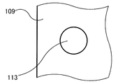
- FIG. 6 is an enlarged plan view of a through hole according to the conventional example.
- a conductive bonding material 105 such as solder is placed on the DCB substrate 104, a semiconductor element 106 is placed thereon, and a conductive bonding material 107 such as solder is further placed thereon (see FIG. FIG. 5 (a)).
- the external terminal 110 is inserted into the recess 112 provided on the surface to which the semiconductor element 106 of the DCB substrate 104 is bonded (FIG. 5B).
- the printed circuit board 109 is set by inserting the external terminal 110 into the through hole 113 formed in the printed circuit board 109 with the printed circuit board 109 with the surface of the post electrode 108 facing the DCB substrate 104 ( FIG. 5 (c)).
- This module is manufactured by batch assembly by N 2 ⁇ H 2 reflow or the like and finally resin-sealing.
- the printed circuit board 109 can be positioned without using a jig by using the through hole 113 and the external terminal 110 as a guide (see, for example, Patent Document 2).
- FIG. 6 shows an enlarged plan view of a printed circuit board and a through hole for an external terminal having a circular cross section.
- the inner diameter of the through hole 113 formed in the printed circuit board 109 is substantially the same as the outer diameter of the external terminal 110 ( ⁇ + 0.05 mm).
- the external terminal 110 is not completely perpendicular to the DCB substrate 104 but is inserted at a slight angle. There is a case.
- the printed circuit board 109 is inserted into the external terminal 110 in such a state, the printed circuit board 109 is also tilted, so that the post electrode 108 may not contact the front surface electrode of the semiconductor element 106. In this case, floating or misalignment occurs between the semiconductor element 106 and the post electrode 108. Therefore, there is a problem that the semiconductor element 106 and the post electrode 108 cannot be bonded by the bonding material 107 such as solder, resulting in a manufacturing defect.
- SiC semiconductor elements which have been applied in recent years, have a size of about 3 mm square, which is smaller than conventional Si semiconductor elements, due to manufacturing yield and the like. For this reason, in order to obtain a large module current capacity using this SiC semiconductor element, it is necessary to mount a plurality of semiconductor elements in one power semiconductor module. Therefore, it is important to secure good positioning accuracy of the printed circuit board 109 for the connection between the post electrode 108 and the semiconductor element 106. For this reason, a large positional deviation of the printed circuit board 109 is a serious problem in manufacturing.
- a semiconductor device includes an insulating substrate having a circuit board on a main surface, a semiconductor element fixed to the circuit board, and one end fixed to the circuit board. And a printed circuit board having a through-hole through which the external terminal penetrates, a rigidity of a peripheral region of the through-hole being lower than a rigidity of another region, and facing a main surface of the insulating substrate. It is set as the structure provided.
- FIG. 1A is a plan view of a semiconductor device according to a first embodiment
- FIG. It is an enlarged plan view of the through hole according to the first embodiment.
- It is the expanded sectional view (a) and enlarged bottom view (b) of the through hole which concern on a 2nd Example.
- It is the top view (a) and sectional drawing (b) of the power semiconductor module which concerns on a prior art example.
- It is the schematic diagram which showed the manufacturing process of the power semiconductor module which concerns on a prior art example.
- It is an enlarged plan view of a through hole according to a conventional example.
- FIG. 1A is a plan view of a semiconductor device according to the first embodiment
- FIG. FIG. 2B is a cross-sectional view of the main part taken along the line II ′ of FIG.
- a power semiconductor module (semiconductor device) 50 shown in the figure has a structure in which a DCB substrate 4 and a printed circuit board 9 opposed to the DCB substrate 4 are integrated by a sealing resin 11.
- a semiconductor element 6 is fixed to the circuit board 3 located on the main surface of the DCB substrate 4.
- the DCB substrate 4 includes an insulating substrate 2, a heat sink 1 formed on the back surface of the insulating substrate 2 by the DCB method, and a circuit board 3 also formed on the main surface of the insulating substrate 2 by the DCB method.
- the circuit board 3 is selectively patterned on the main surface of the insulating substrate 2.
- At least one back electrode (for example, a semiconductor element 6) is formed via a conductive bonding material 5 formed of lead-free solder such as tin (Sn) -silver (Ag). , Collector electrode) are joined.
- the semiconductor element 6 is, for example, an IGBT (Insulated Gate Bipolar Transistor: Insulated Gate Bipolar Transistor), a power MOSFET (Metal Oxide Semiconductor Field Transistor Transducer), or a FWD (Free Wheeled Semiconductor power element).
- IGBT Insulated Gate Bipolar Transistor: Insulated Gate Bipolar Transistor
- MOSFET Metal Oxide Semiconductor Field Transistor Transducer
- FWD Free Wheeled Semiconductor power element
- the insulating substrate 2 is made of ceramic such as alumina (Al 2 O 3 ) sintered body, silicon nitride (Si 3 N 4 ), and the heat sink 1 and the circuit board 3 are mainly composed of copper (Cu). Consists of metal.
- DCB substrate 4 formed by the DCB method
- AMB Active Metal Brazing
- the printed circuit board 9 has a metal layer 14 selectively patterned on its main surface.
- the material of the printed circuit board 9 is, for example, a polyimide resin, an epoxy resin, or the like. Moreover, you may impregnate the inside with the glass cloth comprised by glass fiber as needed.
- the metal layer 14 is comprised by the main component, for example.
- a plurality of holes whose inner walls are treated with a plating layer are provided in the printed circuit board 9 immediately above the region where the front surface electrode (for example, the emitter electrode) of the semiconductor element 6 is located. It has been. And the cylindrical post electrode 8 is inject
- the material of the post electrode 8 is mainly composed of, for example, copper, aluminum (Al), tin-silver lead-free solder material, or an alloy made of these metals. Moreover, the length of each post electrode 8 is uniform.
- the power semiconductor module 50 has an external terminal 10 that is also used for positioning and is fixedly fitted into a recess 12 for external terminal insertion provided on the circuit board 3.
- the printed circuit board 9 has a positioning through hole 13 through which the external terminal 10 passes.
- the fixing strength between the circuit board 3 and the external terminal 10 can be secured by fitting and solder fixing.
- the sealing resin 11 is arrange
- This embodiment is different from the prior art in that the rigidity of the peripheral area of the through hole 13 in the printed board 9 into which the external terminal 10 is inserted for positioning is lower than the rigidity of other areas. More specifically, radial slits 15 are arranged in the peripheral region of the through hole 13. By reducing the rigidity of the peripheral region, only the peripheral region of the through hole 13 can be deformed even when the external terminal 10 is slightly inclined or deformed. Thereby, since the inclination of the whole printed circuit board 9 and position shift can be suppressed, the favorable positioning accuracy of the post electrode 8 can be ensured. As a result, the connection failure between the post electrode 8 and the semiconductor element 6 can be eliminated, and the yield rate of the power semiconductor module 50 can be improved.
- FIG. 2 is an enlarged plan view of the through hole according to the first embodiment.
- FIG. 2A shows a through hole 13 for positioning using the external terminal 10 having a circular cross section, and four slits 15 are arranged radially and symmetrically in the peripheral area of the through hole 13. ing.
- FIG. 2B shows a through hole 13 for positioning using the external terminal 10 having a quadrangular cross section, and slits 15 are arranged in the peripheral area from four corners.
- the corners of the external terminals 10 are most easily in contact with the through holes 13, so it is effective to arrange the slits 15 at the corners of the through holes 13 on the side of the printed circuit board 9 to be penetrated. It is.
- the number of slits 15 may be any number as long as it can be arranged radially and symmetrically. However, considering the additional process of forming slits 15 and the effect of arranging slits 15, about 4 to 8 slits are preferable.
- FIG. 3 is an enlarged cross-sectional view (a) and an enlarged bottom view (b) of the through hole according to the second embodiment.
- a mortar-shaped chamfered portion 16 is provided in the vicinity of the through hole 13 on the surface of the printed circuit board 9 facing the insulating substrate 2 so as to be substantially coaxial with the through hole 13.
- the provision of the chamfered portion 16 makes it possible to insert the external terminal 10 into the through hole 13 while increasing the positioning accuracy while reducing the rigidity of the peripheral region. In the case where the positioning accuracy is further increased, even if the external terminal 10 is slightly inclined, the post electrode 8 can be reliably connected to a predetermined location by the action of the slit 15 described above. It is valid.
Landscapes
- Cooling Or The Like Of Semiconductors Or Solid State Devices (AREA)
- Structures For Mounting Electric Components On Printed Circuit Boards (AREA)
- Structures Or Materials For Encapsulating Or Coating Semiconductor Devices Or Solid State Devices (AREA)
Abstract
スルーホールが設けられているプリント基板の位置決め精度を確保するとともに、外部端子が傾いていても確実にスルーホールに外部端子を挿入することができる。 半導体素子(6)が接合されたDCB基板(4)と、DCB基板(4)に設けられた凹部(12)に挿入された外部端子(10)と、スルーホール(13)及びDCB基板(4)に対向するよう配置されたポスト電極(8)を有するプリント基板(9)とを備えた半導体装置(50)において、外部端子(10)を挿入されているプリント基板(9)のスルーホール(13)の周縁領域にスリット(15)が形成されている。
Description
本発明は、半導体装置に関し、特にパワー半導体素子を搭載したパワー半導体モジュールに関する。
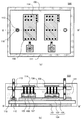
図4は、従来例に係るパワー半導体モジュールの平面図(a)及び断面図(b)である。なお、同図(b)は同図(a)のIII-III’線で切断した要部断面図である。
図4において、パワー半導体モジュール500は、DCB(Direct Copper Bonding)基板104と、半導体素子106と、ポスト電極108と、外部端子110と、プリント基板109とで構成されている。
図4において、パワー半導体モジュール500は、DCB(Direct Copper Bonding)基板104と、半導体素子106と、ポスト電極108と、外部端子110と、プリント基板109とで構成されている。
DCB基板104は、主面に回路板103を有している。半導体素子106は、回路板103に接合材105を介して裏面が固着されている。ポスト電極108は、半導体素子106の表面に接合材107を介して固着されている。外部端子110は、回路板103に設けられた外部端子挿入用の凹部112に導電性の接合材(図示せず)を介して固着されている。プリント基板109は、金属層114を有し、ポスト電極108が固着されている。
このパワー半導体モジュール500は、半導体素子106の裏面電極(図示せず)への電気配線を回路板103で行い、半導体素子106のおもて面電極(図示せず)への電気配線をポスト電極108及び金属層114を備えたプリント基板109で行う構造となっている(例えば、特許文献1参照)。
パワー半導体モジュール500の製造工程を図5に示す。
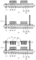
図5は、従来例に係るパワー半導体モジュールの製造工程を示した模式図であり、図6は、従来例に係るスルーホールの拡大平面図である。
図5は、従来例に係るパワー半導体モジュールの製造工程を示した模式図であり、図6は、従来例に係るスルーホールの拡大平面図である。
まず、DCB基板104に半田等の導電性の接合材105を載置した後、その上に半導体素子106を載置し、さらにその上に半田等の導電性の接合材107を載置する(図5(a))。次に、DCB基板104の半導体素子106が接合される面に設けられた凹部112に、外部端子110を挿入する(図5(b))。さらに、ポスト電極108の面をDCB基板104と対向する面に向けたプリント基板109を、プリント基板109に形成されたスルーホール113に外部端子110を挿入することで、プリント基板109をセットする(図5(c))。このモジュールをN2・H2リフロー等により一括組立し、最後に樹脂封止することで製造される。この方法では、プリント基板109はスルーホール113を利用し外部端子110をガイドとすることで、治具を使わずに位置決めが可能である(例えば、特許文献2参照)。
ここで、図6にプリント基板と円状の断面を持つ外部端子用のスルーホールの拡大した平面図を示す。
プリント基板109に形成されたスルーホール113の内径は、外部端子110の外径とほぼ同じ(~+0.05mm)となっている。
プリント基板109に形成されたスルーホール113の内径は、外部端子110の外径とほぼ同じ(~+0.05mm)となっている。
パワー半導体モジュール500の製造時において、凹部112に外部端子110を挿入した際(図5(b))、外部端子110はDCB基板104に対して完全に垂直ではなく、わずかに傾いて挿入される場合がある。このような状態で、外部端子110にプリント基板109を挿入すると、プリント基板109にも傾きが生じることからポスト電極108が半導体素子106のおもて面電極に接触しない場合がある。この場合、半導体素子106とポスト電極108との間に浮きや位置ズレが生じる。そのため、半導体素子106とポスト電極108が半田等の接合材107で接合できず、製造不良となる課題があった。
この課題に対しては、プリント基板109のスルーホール113の内径を、外部端子110の内径に比べ大きくすることにより、外部端子110の傾き等の影響は少なくなる。しかしその場合は、プリント基板109自体の位置ズレが大きくなるという課題が新たに発生する。
特に近年適用が進むSiC半導体素子は、製造歩留まり等の関係から素子の大きさが約3mm角と従来のSi半導体素子と比べ小さい。このため、このSiC半導体素子を用いて大きなモジュール電流容量を得るためには、複数の半導体素子を一つのパワー半導体モジュールに搭載する必要がある。そこで、ポスト電極108と半導体素子106の接続にはプリント基板109の良好な位置決め精度の確保が重要となる。このため、プリント基板109の位置ズレが大きくなるのは製造上大きな問題である。
前記の目的を達成するために、この発明の一態様では、半導体装置は、主面に回路板を有する絶縁基板と、前記回路板に固着されている半導体素子と、前記回路板に一端が固着されている外部端子と、前記外部端子が貫通するスルーホールを有し、前記スルーホールの周縁領域の剛性が他の領域の剛性よりも低く、前記絶縁基板の主面に対向するプリント基板とを備えた構成とする。
上記の手段によれば、パワー半導体モジュールを構成するDCB基板の凹部に挿入された外部端子にわずかな傾きがある場合でも、プリント基板の浮きや位置ズレが原因となる接続不良を少なくすることができる。このため、パワー半導体モジュールの組立良品率向上を実現することが可能となっている。
本発明の上記及び他の目的、特徴及び利点は本発明の例として好ましい実施の形態を表す添付の図面と関連した以下の説明により明らかになるであろう。
以下に、本発明の好適な実施形態(実施例)を図面に基づいて説明する。
実施の形態を通して共通の構成には同一の符号を付すものとし、重複する説明は省略する。
実施の形態を通して共通の構成には同一の符号を付すものとし、重複する説明は省略する。
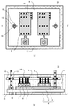
図1は、第1の実施例に係る半導体装置の平面図(a)及び断面図(b)である。
なお、同図(b)は同図(a)のI-I’線で切断した要部断面図である。
図示するパワー半導体モジュール(半導体装置)50は、DCB基板4と、DCB基板4に対向させたプリント基板9とが封止樹脂11により一体的になった構造をなしている。そして、DCB基板4の主面に位置する回路板3に、半導体素子6が固着されている。
なお、同図(b)は同図(a)のI-I’線で切断した要部断面図である。
図示するパワー半導体モジュール(半導体装置)50は、DCB基板4と、DCB基板4に対向させたプリント基板9とが封止樹脂11により一体的になった構造をなしている。そして、DCB基板4の主面に位置する回路板3に、半導体素子6が固着されている。
DCB基板4は、絶縁基板2と、絶縁基板2の裏面にDCB法で形成された放熱板1と、絶縁基板2の主面に同じくDCB法で形成された回路板3を備えている。回路板3は、絶縁基板2の主面に選択的にパターン形成されている。
さらに、回路板3上には、錫(Sn)-銀(Ag)系等の鉛フリー半田等で形成される導電性の接合材5を介して、少なくとも一つの半導体素子6の裏面電極(例えば、コレクタ電極)が接合されている。
ここで半導体素子6は、例えばIGBT(Insulated Gate Bipolar Transistor:絶縁ゲートバイポーラトランジスタ)、パワーMOSFET(Metal Oxide Semiconductor Field Effect Transistor)、FWD(Free Wheeling Diode)等の縦型のパワー半導体素子が該当する。
また絶縁基板2は、例えばアルミナ(Al2O3)焼結体、窒化シリコン(Si3N4)等のセラミックで構成され、放熱板1、回路板3は銅(Cu)を主成分とする金属で構成されている。
なおDCB法により形成されたDCB基板4だけでなく、絶縁基板2に放熱板1、回路板3をロー材によって接合したAMB(Active Metal Brazing)基板を用いてもよい。
プリント基板9は、その主面に金属層14が選択的にパターン形成されている。ここで、プリント基板9の材質は、例えば、ポリイミド樹脂、エポキシ樹脂等である。また必要に応じて、ガラス繊維で構成されたガラスクロスを内部に含浸させてもよい。また金属層14は、例えば、銅を主たる成分により構成されている。
パワー半導体モジュール50においては、半導体素子6のおもて面電極(例えばエミッタ電極)が位置する領域直上のプリント基板9に、内壁がめっき層(図示せず)で処理された複数の孔が設けられている。そして、その孔の内に円筒状のポスト電極8がめっき層を介し注入(インプラント)されている。さらに各々のポスト電極8は、プリント基板9の主面に配設された金属層14と導通された状態にある。上記により、パワー半導体モジュール50においては、半導体素子6のおもて面電極と、外部回路との電気的な接続が、ポスト電極8並びに金属層14を経由して確保されている。なお、半導体素子6の裏面電極と、外部回路との電気的な接続については、回路板3を経由して確保されている。
なおポスト電極8の材質は、例えば、銅、アルミニウム(Al)、錫-銀系の鉛フリーの半田材、または、これらの金属からなる合金を主たる成分で構成されている。また、各々のポスト電極8の長さは、均一である。
さらにパワー半導体モジュール50は、回路板3に設けられた外部端子挿入用の凹部12に嵌合して固着される位置決め兼用の外部端子10を有している。そしてプリント基板9は、外部端子10が貫通する位置決め用のスルーホール13を有している。
凹部12と外部端子10を、図示しない半田を介して固着することで、嵌合と半田固着により、回路板3と外部端子10の固着強度を確保することができる。
また上記構成要素を外部環境から保護するため、封止樹脂11が上記構成要素の周囲に配置されている。これにより、パワー半導体モジュール50の動作時における発熱・冷却で生じる半導体素子6及び導電性の接合材5、7への応力が緩和され、信頼性の高いパワー半導体モジュールを実現することができる。
また上記構成要素を外部環境から保護するため、封止樹脂11が上記構成要素の周囲に配置されている。これにより、パワー半導体モジュール50の動作時における発熱・冷却で生じる半導体素子6及び導電性の接合材5、7への応力が緩和され、信頼性の高いパワー半導体モジュールを実現することができる。
本実施例が従来技術と異なる点は、位置決めのため外部端子10を挿入するプリント基板9内のスルーホール13の周縁領域の剛性を、他の領域の剛性よりも低くしている点である。より具体的には、スルーホール13の周縁領域に放射状のスリット15が配置されている点である。周縁領域の剛性を低くすることにより、外部端子10のわずかな傾きや変形が生じた場合でも、スルーホール13の周縁領域のみ変形させることができる。これによりプリント基板9全体の傾き、位置ズレを抑えることができることから、ポスト電極8の良好な位置決め精度を確保することができる。この結果、ポスト電極8と半導体素子6の接続不良をなくし、パワー半導体モジュール50の良品率を改善することができる。
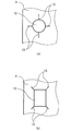
図2は、第1の実施例に係るスルーホールの拡大平面図である。
図2(a)は、断面円形状の外部端子10を用いて位置決めするためのスルーホール13を示したものであり、スルーホール13の周縁領域に放射状かつ対称に4本のスリット15が配置されている。
図2(a)は、断面円形状の外部端子10を用いて位置決めするためのスルーホール13を示したものであり、スルーホール13の周縁領域に放射状かつ対称に4本のスリット15が配置されている。
また図2(b)は、断面四角形状の外部端子10を用いて位置決めするためのスルーホール13を示したものであり、四つの角から周縁領域にそれぞれスリット15が配置されている。外部端子10及びスルーホール13が四角の場合、外部端子10の角が最もスルーホール13に接触しやすいため、貫通させるプリント基板9側のスルーホール13の角にスリット15が配置されることが有効である。
また上記のようにスリット15を放射状かつ対称に配置することで、プリント基板9の位置が、ある一方向に矯正(位置決め)されにくくできるため有効である。なおスリット15の数は放射状かつ対称に配置することができれば何本でも良いが、スリット15を形成する追加工程及びスリット15を配置する効果を勘案すると、4~8本程度が好ましい。
また外部端子10及びスルーホール13の断面形状は5~8角形等も可能であり、この場合はスルーホール13側の角にスリット15を形成することが有効である。
図3は、第2の実施例に係るスルーホールの拡大断面図(a)及び拡大底面図(b)である。
図3は、第2の実施例に係るスルーホールの拡大断面図(a)及び拡大底面図(b)である。
この実施例においては、プリント基板9の絶縁基板2と対向する面のうち、スルーホール13の近傍に、スルーホール13と略同軸となるよう、すり鉢形状の面取り部16が設けられている。
この面取り部16が設けられることにより、周縁領域の剛性を低くするのと同時に、位置決め精度をより高めながら外部端子10をスルーホール13に挿入することが可能となる。そして位置決め精度がより高められた場合において、外部端子10がわずかに傾いていたとしても、上記に示したスリット15の働きにより確実にポスト電極8を所定の箇所に接続することができるため、より有効である。
上記については単に本発明の原理を示すものである。さらに、多数の変形、変更が当業者にとって可能であり、本発明は上記に示し、説明した正確な構成及び応用例に限定されるものではない。そして、対応するすべての変形例及び均等物は、添付の請求項及びその均等物による本発明の範囲とみなされる。
1 放熱板
2 絶縁基板
3、103 回路板
4、104 DCB基板
5、7、105、107 接合材
6、106 半導体素子
8、108 ポスト電極
9、109 プリント基板
10、110 外部端子
11 封止樹脂
12、112 凹部
13、113 スルーホール
14、114 金属層
15 スリット
16 面取り部
50、500 パワー半導体モジュール
2 絶縁基板
3、103 回路板
4、104 DCB基板
5、7、105、107 接合材
6、106 半導体素子
8、108 ポスト電極
9、109 プリント基板
10、110 外部端子
11 封止樹脂
12、112 凹部
13、113 スルーホール
14、114 金属層
15 スリット
16 面取り部
50、500 パワー半導体モジュール
Claims (8)
- 主面に回路板を有する絶縁基板と、
前記回路板に固着されている半導体素子と、
前記回路板に一端が固着されている外部端子と、
前記外部端子が貫通するスルーホールを有し、前記スルーホールの周縁領域の剛性が他の領域の剛性よりも低く、前記絶縁基板の主面に対向するプリント基板と、
を備えた半導体装置。 - 前記半導体素子はおもて面に電極を有し、
一端が前記半導体素子の電極に固着され、他端が前記プリント基板に固着されているポスト電極を備えた請求項1記載の半導体装置。 - 前記周縁領域にスリットが設けられている請求項1記載の半導体装置。
- 前記スリットが、一つの前記周縁領域に複数個設けられている請求項3記載の半導体装置。
- 前記スルーホールが平面円形状であり、
前記スリットが前記プリント基板の主面側から見て、放射状かつ均一な角度になるように設けられている請求項4記載の半導体装置。 - 前記スルーホールが平面多角形状であり、
前記スリットが前記プリント基板の主面側から見て、それぞれの角の頂点から放射状に設けられている請求項4記載の半導体装置。 - 前記平面多角形状が、平面四角形状である請求項6記載の半導体装置。
- 前記プリント基板の前記絶縁基板と対向する面の前記周縁領域に、面取り部が設けられている請求項1記載の半導体装置。
Priority Applications (3)
| Application Number | Priority Date | Filing Date | Title |
|---|---|---|---|
| JP2015600133U JP3203387U (ja) | 2013-06-05 | 2014-05-08 | 半導体装置 |
| CN201490000642.5U CN205264696U (zh) | 2013-06-05 | 2014-05-08 | 半导体装置 |
| US14/933,449 US9640454B2 (en) | 2013-06-05 | 2015-11-05 | Semiconductor device |
Applications Claiming Priority (2)
| Application Number | Priority Date | Filing Date | Title |
|---|---|---|---|
| JP2013118495A JP2016006806A (ja) | 2013-06-05 | 2013-06-05 | 半導体装置 |
| JP2013-118495 | 2013-06-05 |
Related Child Applications (1)
| Application Number | Title | Priority Date | Filing Date |
|---|---|---|---|
| US14/933,449 Continuation US9640454B2 (en) | 2013-06-05 | 2015-11-05 | Semiconductor device |
Publications (1)
| Publication Number | Publication Date |
|---|---|
| WO2014196309A1 true WO2014196309A1 (ja) | 2014-12-11 |
Family
ID=52007962
Family Applications (1)
| Application Number | Title | Priority Date | Filing Date |
|---|---|---|---|
| PCT/JP2014/062389 Ceased WO2014196309A1 (ja) | 2013-06-05 | 2014-05-08 | 半導体装置 |
Country Status (4)
| Country | Link |
|---|---|
| US (1) | US9640454B2 (ja) |
| JP (2) | JP2016006806A (ja) |
| CN (1) | CN205264696U (ja) |
| WO (1) | WO2014196309A1 (ja) |
Cited By (3)
| Publication number | Priority date | Publication date | Assignee | Title |
|---|---|---|---|---|
| CN105246286A (zh) * | 2015-11-17 | 2016-01-13 | 杨友林 | 电力半导体器件综合保护装置及制备方法 |
| CN105471415A (zh) * | 2016-01-12 | 2016-04-06 | 陈勤华 | 智能固态继电器 |
| US20220077103A1 (en) * | 2020-09-10 | 2022-03-10 | Fuji Electric Co., Ltd. | Semiconductor device and manufacturing method of semiconductor device |
Families Citing this family (12)
| Publication number | Priority date | Publication date | Assignee | Title |
|---|---|---|---|---|
| US9681558B2 (en) | 2014-08-12 | 2017-06-13 | Infineon Technologies Ag | Module with integrated power electronic circuitry and logic circuitry |
| US10211158B2 (en) * | 2014-10-31 | 2019-02-19 | Infineon Technologies Ag | Power semiconductor module having a direct copper bonded substrate and an integrated passive component, and an integrated power module |
| JP6866716B2 (ja) * | 2017-03-23 | 2021-04-28 | 富士電機株式会社 | 半導体装置 |
| JP7214966B2 (ja) * | 2018-03-16 | 2023-01-31 | 富士電機株式会社 | 半導体装置及び半導体装置の製造方法 |
| JP6884723B2 (ja) | 2018-03-23 | 2021-06-09 | 株式会社東芝 | 半導体装置 |
| US10748831B2 (en) * | 2018-05-30 | 2020-08-18 | Taiwan Semiconductor Manufacturing Co., Ltd. | Semiconductor packages having thermal through vias (TTV) |
| CN112913009B (zh) * | 2019-04-10 | 2024-08-16 | 新电元工业株式会社 | 半导体装置以及引线框材料 |
| JP7380124B2 (ja) * | 2019-11-20 | 2023-11-15 | 富士電機株式会社 | 電力用半導体モジュール及び電力用半導体モジュールの製造方法 |
| JP7476540B2 (ja) * | 2020-01-23 | 2024-05-01 | 富士電機株式会社 | 半導体装置 |
| KR102930056B1 (ko) * | 2020-09-16 | 2026-02-24 | 에스케이하이닉스 주식회사 | 관통 전극을 포함하는 반도체 칩, 및 이 반도체 칩을 포함하는 반도체 패키지 |
| JP7720182B2 (ja) * | 2021-07-12 | 2025-08-07 | 新電元工業株式会社 | 半導体装置 |
| JP2025043996A (ja) * | 2023-09-19 | 2025-04-01 | 株式会社日立産機システム | プリント配線板 |
Citations (4)
| Publication number | Priority date | Publication date | Assignee | Title |
|---|---|---|---|---|
| JPH0951152A (ja) * | 1995-08-08 | 1997-02-18 | Saginomiya Seisakusho Inc | フレキシブル基板の取付け構造及び取付け方法 |
| JP2005285919A (ja) * | 2004-03-29 | 2005-10-13 | Japan Aviation Electronics Industry Ltd | フレキシブル配線板 |
| JP2010278093A (ja) * | 2009-05-27 | 2010-12-09 | Diamond Electric Mfg Co Ltd | 車載用半導体装置 |
| JP2012129336A (ja) * | 2010-12-15 | 2012-07-05 | Fuji Electric Co Ltd | 半導体装置およびその製造方法 |
Family Cites Families (2)
| Publication number | Priority date | Publication date | Assignee | Title |
|---|---|---|---|---|
| JP5241177B2 (ja) | 2007-09-05 | 2013-07-17 | 株式会社オクテック | 半導体装置及び半導体装置の製造方法 |
| JP5531974B2 (ja) | 2011-01-21 | 2014-06-25 | 住友電装株式会社 | コネクタ及び端子整列部材 |
-
2013
- 2013-06-05 JP JP2013118495A patent/JP2016006806A/ja active Pending
-
2014
- 2014-05-08 JP JP2015600133U patent/JP3203387U/ja not_active Expired - Fee Related
- 2014-05-08 WO PCT/JP2014/062389 patent/WO2014196309A1/ja not_active Ceased
- 2014-05-08 CN CN201490000642.5U patent/CN205264696U/zh not_active Expired - Fee Related
-
2015
- 2015-11-05 US US14/933,449 patent/US9640454B2/en not_active Expired - Fee Related
Patent Citations (4)
| Publication number | Priority date | Publication date | Assignee | Title |
|---|---|---|---|---|
| JPH0951152A (ja) * | 1995-08-08 | 1997-02-18 | Saginomiya Seisakusho Inc | フレキシブル基板の取付け構造及び取付け方法 |
| JP2005285919A (ja) * | 2004-03-29 | 2005-10-13 | Japan Aviation Electronics Industry Ltd | フレキシブル配線板 |
| JP2010278093A (ja) * | 2009-05-27 | 2010-12-09 | Diamond Electric Mfg Co Ltd | 車載用半導体装置 |
| JP2012129336A (ja) * | 2010-12-15 | 2012-07-05 | Fuji Electric Co Ltd | 半導体装置およびその製造方法 |
Cited By (4)
| Publication number | Priority date | Publication date | Assignee | Title |
|---|---|---|---|---|
| CN105246286A (zh) * | 2015-11-17 | 2016-01-13 | 杨友林 | 电力半导体器件综合保护装置及制备方法 |
| CN105471415A (zh) * | 2016-01-12 | 2016-04-06 | 陈勤华 | 智能固态继电器 |
| US20220077103A1 (en) * | 2020-09-10 | 2022-03-10 | Fuji Electric Co., Ltd. | Semiconductor device and manufacturing method of semiconductor device |
| US12230600B2 (en) * | 2020-09-10 | 2025-02-18 | Fuji Electric Co., Ltd. | Semiconductor device having through parts of different shapes |
Also Published As
| Publication number | Publication date |
|---|---|
| US9640454B2 (en) | 2017-05-02 |
| JP2016006806A (ja) | 2016-01-14 |
| JP3203387U (ja) | 2016-03-31 |
| US20160079133A1 (en) | 2016-03-17 |
| CN205264696U (zh) | 2016-05-25 |
Similar Documents
| Publication | Publication Date | Title |
|---|---|---|
| JP3203387U (ja) | 半導体装置 | |
| JP6032294B2 (ja) | 半導体装置 | |
| JP4613077B2 (ja) | 半導体装置、電極用部材および電極用部材の製造方法 | |
| JP2022179649A (ja) | 半導体装置及びその製造方法 | |
| US9877397B2 (en) | Mounting jig for semiconductor device | |
| JP6206494B2 (ja) | 半導体装置 | |
| US10242961B2 (en) | Semiconductor device | |
| JP5930070B2 (ja) | 半導体装置 | |
| JP5970348B2 (ja) | 半導体装置 | |
| CN107527883A (zh) | 半导体装置及其制造方法以及导电柱 | |
| JP5732880B2 (ja) | 半導体装置及びその製造方法 | |
| US20170194296A1 (en) | Semiconductor module | |
| JP2016146450A (ja) | 電子装置 | |
| US12519047B2 (en) | Semiconductor device | |
| US20200266130A1 (en) | Semiconductor device | |
| US20230092121A1 (en) | Semiconductor device | |
| JP2017034224A (ja) | 電子モジュール | |
| JP2017063168A (ja) | 回路基板および電子装置 | |
| US11978683B2 (en) | Semiconductor apparatus | |
| JP6603098B2 (ja) | 回路基板および電子装置 | |
| CN111602240B (zh) | 树脂封装型半导体装置 | |
| JP2021034701A (ja) | 半導体装置 | |
| JP7604815B2 (ja) | 半導体装置および半導体装置の製造方法 | |
| US20250079383A1 (en) | Semiconductor device | |
| JP2020155623A (ja) | 半導体装置 |
Legal Events
| Date | Code | Title | Description |
|---|---|---|---|
| 121 | Ep: the epo has been informed by wipo that ep was designated in this application |
Ref document number: 14807789 Country of ref document: EP Kind code of ref document: A1 |
|
| ENP | Entry into the national phase |
Ref document number: 2015600133 Country of ref document: JP Kind code of ref document: A |
|
| NENP | Non-entry into the national phase |
Ref country code: DE |
|
| 122 | Ep: pct application non-entry in european phase |
Ref document number: 14807789 Country of ref document: EP Kind code of ref document: A1 |