WO2014196253A1 - p型選択エミッタ形成方法及び太陽電池 - Google Patents
p型選択エミッタ形成方法及び太陽電池 Download PDFInfo
- Publication number
- WO2014196253A1 WO2014196253A1 PCT/JP2014/059448 JP2014059448W WO2014196253A1 WO 2014196253 A1 WO2014196253 A1 WO 2014196253A1 JP 2014059448 W JP2014059448 W JP 2014059448W WO 2014196253 A1 WO2014196253 A1 WO 2014196253A1
- Authority
- WO
- WIPO (PCT)
- Prior art keywords
- film
- dopant
- diffusion layer
- selective emitter
- organosilicon compound
- Prior art date
- Legal status (The legal status is an assumption and is not a legal conclusion. Google has not performed a legal analysis and makes no representation as to the accuracy of the status listed.)
- Ceased
Links
Images
Classifications
-
- H—ELECTRICITY
- H10—SEMICONDUCTOR DEVICES; ELECTRIC SOLID-STATE DEVICES NOT OTHERWISE PROVIDED FOR
- H10P—GENERIC PROCESSES OR APPARATUS FOR THE MANUFACTURE OR TREATMENT OF DEVICES COVERED BY CLASS H10
- H10P32/00—Diffusion of dopants within, into or out of wafers, substrates or parts of devices
- H10P32/10—Diffusion of dopants within, into or out of semiconductor bodies or layers
- H10P32/14—Diffusion of dopants within, into or out of semiconductor bodies or layers within a single semiconductor body or layer in a solid phase; between different semiconductor bodies or layers, both in a solid phase
- H10P32/1408—Diffusion of dopants within, into or out of semiconductor bodies or layers within a single semiconductor body or layer in a solid phase; between different semiconductor bodies or layers, both in a solid phase from or through or into an external applied layer, e.g. photoresist or nitride layers
-
- H—ELECTRICITY
- H10—SEMICONDUCTOR DEVICES; ELECTRIC SOLID-STATE DEVICES NOT OTHERWISE PROVIDED FOR
- H10F—INORGANIC SEMICONDUCTOR DEVICES SENSITIVE TO INFRARED RADIATION, LIGHT, ELECTROMAGNETIC RADIATION OF SHORTER WAVELENGTH OR CORPUSCULAR RADIATION
- H10F10/00—Individual photovoltaic cells, e.g. solar cells
- H10F10/10—Individual photovoltaic cells, e.g. solar cells having potential barriers
- H10F10/14—Photovoltaic cells having only PN homojunction potential barriers
-
- H—ELECTRICITY
- H10—SEMICONDUCTOR DEVICES; ELECTRIC SOLID-STATE DEVICES NOT OTHERWISE PROVIDED FOR
- H10F—INORGANIC SEMICONDUCTOR DEVICES SENSITIVE TO INFRARED RADIATION, LIGHT, ELECTROMAGNETIC RADIATION OF SHORTER WAVELENGTH OR CORPUSCULAR RADIATION
- H10F71/00—Manufacture or treatment of devices covered by this subclass
- H10F71/121—The active layers comprising only Group IV materials
-
- H—ELECTRICITY
- H10—SEMICONDUCTOR DEVICES; ELECTRIC SOLID-STATE DEVICES NOT OTHERWISE PROVIDED FOR
- H10P—GENERIC PROCESSES OR APPARATUS FOR THE MANUFACTURE OR TREATMENT OF DEVICES COVERED BY CLASS H10
- H10P32/00—Diffusion of dopants within, into or out of wafers, substrates or parts of devices
- H10P32/10—Diffusion of dopants within, into or out of semiconductor bodies or layers
- H10P32/17—Diffusion of dopants within, into or out of semiconductor bodies or layers characterised by the semiconductor material
- H10P32/171—Diffusion of dopants within, into or out of semiconductor bodies or layers characterised by the semiconductor material being group IV material
-
- H—ELECTRICITY
- H10—SEMICONDUCTOR DEVICES; ELECTRIC SOLID-STATE DEVICES NOT OTHERWISE PROVIDED FOR
- H10P—GENERIC PROCESSES OR APPARATUS FOR THE MANUFACTURE OR TREATMENT OF DEVICES COVERED BY CLASS H10
- H10P32/00—Diffusion of dopants within, into or out of wafers, substrates or parts of devices
- H10P32/10—Diffusion of dopants within, into or out of semiconductor bodies or layers
- H10P32/19—Diffusion sources
-
- Y—GENERAL TAGGING OF NEW TECHNOLOGICAL DEVELOPMENTS; GENERAL TAGGING OF CROSS-SECTIONAL TECHNOLOGIES SPANNING OVER SEVERAL SECTIONS OF THE IPC; TECHNICAL SUBJECTS COVERED BY FORMER USPC CROSS-REFERENCE ART COLLECTIONS [XRACs] AND DIGESTS
- Y02—TECHNOLOGIES OR APPLICATIONS FOR MITIGATION OR ADAPTATION AGAINST CLIMATE CHANGE
- Y02E—REDUCTION OF GREENHOUSE GAS [GHG] EMISSIONS, RELATED TO ENERGY GENERATION, TRANSMISSION OR DISTRIBUTION
- Y02E10/00—Energy generation through renewable energy sources
- Y02E10/50—Photovoltaic [PV] energy
- Y02E10/547—Monocrystalline silicon PV cells
-
- Y—GENERAL TAGGING OF NEW TECHNOLOGICAL DEVELOPMENTS; GENERAL TAGGING OF CROSS-SECTIONAL TECHNOLOGIES SPANNING OVER SEVERAL SECTIONS OF THE IPC; TECHNICAL SUBJECTS COVERED BY FORMER USPC CROSS-REFERENCE ART COLLECTIONS [XRACs] AND DIGESTS
- Y02—TECHNOLOGIES OR APPLICATIONS FOR MITIGATION OR ADAPTATION AGAINST CLIMATE CHANGE
- Y02P—CLIMATE CHANGE MITIGATION TECHNOLOGIES IN THE PRODUCTION OR PROCESSING OF GOODS
- Y02P70/00—Climate change mitigation technologies in the production process for final industrial or consumer products
- Y02P70/50—Manufacturing or production processes characterised by the final manufactured product
Definitions
- the present invention uses a film made of an organosilicon compound as a diffusion suppression mask for suppressing diffusion of a dopant, and forms a selective emitter layer in a p layer, and a p-type selective emitter layer formed by this formation method. It has a solar cell.
- a solar cell is a semiconductor element that converts light energy into electric power, and includes a pn junction type, a pin type, a Schottky type, and the pn junction type is widely used. Further, when solar cells are classified based on their substrate materials, they are broadly classified into three types: silicon crystal solar cells, amorphous (amorphous) silicon solar cells, and compound semiconductor solar cells. Silicon crystal solar cells are further classified into single crystal solar cells and polycrystalline solar cells. Since the silicon crystal substrate for solar cells can be manufactured relatively easily, its production scale is currently the largest, and it is expected that it will become more popular in the future (for example, Patent Document 1: JP-A-8-073297). Publication).
- the output characteristics of a solar cell are generally evaluated by measuring an output current voltage curve using a solar simulator.
- the light-receiving surface and back surface of the silicon substrate are protected by an insulating film except for the contact portion with the electrode, and carrier recombination at the interface between the silicon substrate and the insulating film is suppressed and converted.
- the efficiency ⁇ is improved.
- Patent Document 2 Japanese Patent Application Laid-Open No. 2007-081300 proposes a method of applying a silicon oxide film to a diffusion control mask (diffusion suppression mask) to form a patterned diffusion layer.
- a diffusion control mask diffusion suppression mask
- a diffusion layer cannot be formed.
- Patent Document 3 Japanese Patent Application Laid-Open No. 2004-2211409 proposes that a plurality of types of coating agents are separately applied by an ink jet method to create regions with different dopant concentrations and dopant types in a simple process. ing.
- an ink jet system when phosphoric acid or the like is used as a dopant, a countermeasure against corrosion is necessary, and the apparatus becomes complicated and maintenance becomes complicated. Further, even if coating agents having different dopant concentrations and types are applied separately by inkjet, if the diffusion is performed by a single heat treatment, a desired concentration difference cannot be obtained by autodoping.
- Patent Document 4 Japanese Patent Laid-Open No. 2004-28169 proposes a method of forming a low concentration diffusion layer and a high concentration diffusion layer by two heat treatments.
- this method it is necessary to perform thermal diffusion of the dopant twice, which may complicate the process and increase the manufacturing cost.
- the heat treatment is performed once, the dopant is highly concentrated in portions other than the portion immediately below the electrode on the light receiving surface due to autodoping, and high conversion efficiency is not exhibited.
- the present invention has been made in view of the above problems, and provides a solar cell and a p-type selective emitter formation method that can form a p-type selective emitter layer by a simple method and have high energy conversion efficiency.
- the purpose is to do.
- the inventors of the present invention formed a film made of an organosilicon compound on the light receiving surface side of a silicon substrate, and formed a film of an organosilicon compound at a portion corresponding to a p-layer high concentration diffusion region.
- a boron-containing coating agent is applied and diffused over the organic silicon compound film and the opening, so that multiple heat treatment steps are not required, and it is simple and reliable. It has been found that a p-type selective emitter layer can be formed.
- the surface dopant concentration on the light receiving surface should be low in order to improve the conversion efficiency in the short wavelength region, but in order to reduce the electrode contact resistance, it is necessary to increase the dopant concentration. When the dopant concentration in the diffusion layer decreases, ohmic contact cannot be obtained.
- the region of the silicon substrate on the light receiving surface side where the electrode is connected does not form an organic silicon compound film, and other regions are diffused using a film made of an organic silicon compound, Since the high concentration diffusion layer is formed in the region serving as the electrode connection position, the electrode contact resistance can be reduced, while the surface dopant concentration in the film formation region made of the organosilicon compound is lowered, the surface passivation is improved, and the short The conversion efficiency in the wavelength region can be improved, and a p-type selective emitter layer having a high-concentration diffusion layer and a low-concentration diffusion layer in the p-type diffusion layer can be easily formed.
- the present invention provides the following p-type selective emitter formation method and solar cell.
- a solar cell comprising a p-type selective emitter layer formed by the selective emitter formation method according to any one of [1] to [5].
- a solar cell having a p-type selective emitter layer having a high-concentration diffusion layer and a low-concentration diffusion layer can be easily manufactured, and a high-performance solar cell while maintaining a high manufacturing yield. Can be provided.
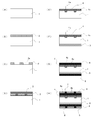
- FIG. 1 are schematic cross-sectional views for sequentially explaining the steps in an example of the method for producing a solar cell of the present invention.
- a solar cell having a p-type selective emitter layer formed by the p-type selective emitter forming method of the present invention is formed on a silicon substrate 1 and a light receiving surface side of the silicon substrate 1,
- a solar cell comprising a light receiving surface electrode 7 to be electrically connected, an n-type diffusion layer 5 formed on the back side of the silicon substrate 1, and a back electrode 8 electrically connected to the n-type diffusion layer 5.
- a film made of an organosilicon compound is formed on the silicon substrate on the side to be the p-type diffusion layer, and the organosilicon compound corresponding to the region to be the electrode connection position of the p-type diffusion layer Part of the membrane
- a dopant is applied on the film made of the organosilicon compound, and the dopant is simultaneously diffused into the silicon substrate through the opening and the film made of the organosilicon compound.
- a p-type selective emitter layer is formed.
- the silicon substrate 1 may be n-type or p-type, but an n-type substrate is used in Example 1 of the present invention.
- This silicon single crystal substrate may be produced by any of the Czochralski (CZ) method and the float zone (FZ) method.
- the specific resistance of the silicon substrate 1 is preferably from 0.1 to 20 ⁇ ⁇ cm, more preferably from 0.5 to 2.0 ⁇ ⁇ cm, from the viewpoint of producing a high-performance solar cell.
- As the silicon substrate a phosphorus-doped n-type single crystal silicon substrate is preferable.
- the phosphorus-doped dopant concentration is preferably 1 ⁇ 10 15 cm ⁇ 3 to 5 ⁇ 10 16 cm ⁇ 3 [FIG. 1 (A)].
- the silicon substrate 1 is immersed in an aqueous sodium hydroxide solution, for example, and the damaged layer is removed by etching.
- a strong alkaline aqueous solution such as potassium hydroxide may be used, and a similar purpose can be achieved with an acid aqueous solution such as hydrofluoric acid.
- a random texture is formed on the substrate 1 subjected to damage etching.
- a solar cell preferably has an uneven shape on the surface. The reason is that in order to reduce the reflectance in the visible light region, it is necessary to cause the light receiving surface to perform reflection at least twice as much as possible.
- the size of each of these peaks is preferably about 1 to 20 ⁇ m.
- Typical surface uneven structures include V-grooves and U-grooves. These can be formed using a grinding machine. In order to create a random concavo-convex structure, a method of performing wet etching by immersing in an aqueous solution of sodium hydroxide and isopropyl alcohol, or acid etching, reactive ion etching, or the like can be used. In the drawing, the texture structure formed on both sides is fine and therefore omitted.
- a film made of an organosilicon compound is formed on the surface of the textured silicon substrate that serves as the light-receiving surface [FIG. 1 (B)].
- the film made of an organosilicon compound include a polysilazane film and a polysiloxane film.
- a method for forming a film in the case of a polysilazane film, a polysilazane solution is applied to the surface to be a light-receiving surface of a silicon substrate, and the solvent is removed by heat drying treatment, whereby a self-crosslinking reaction proceeds and a polysilazane film is formed.
- the method for applying the polysilazane solution is not particularly limited, such as a spin coating method, a spray method, or a dip method, but the spin coating method is simple and suitable.
- the coating composition used for forming the polysilazane solution includes polysilazane and a solvent.
- polysilazane the following general formula (1) -(SiH 2 NH) n- (1)
- the perhydropolysilazane represented by the formula (2) is preferred because there are few impurities remaining in the film after conversion.
- Perhydropolysilazane is an inorganic polymer having — (SiH 2 NH) — as a basic unit, all of its side chains being hydrogen, and being soluble in an organic solvent.
- the solvent may be any solvent that does not react with perhydropolysilazane.
- Aromatic solvents such as hexane, aliphatic solvents, and ether solvents.
- the concentration of polysilazane in the solvent is preferably 1 to 30% by mass, more preferably 3 to 20% by mass. If it is less than 1% by mass, the film thickness after application becomes thin, and there is a possibility that a difference in diffusion concentration in the p-type diffusion layer may not be obtained. If it exceeds 30% by mass, the stability of the solution may be lowered.
- the drying temperature for forming the polysilazane film is not a problem as long as it is equal to or higher than the boiling point of the solvent used, but it is preferable to perform the drying temperature in the range of 80 to 200 ° C.
- the heating method is not particularly limited, and examples thereof include a method of heating with a hot plate and a method of using an electric furnace, and the method of using a hot plate is preferable from the viewpoint of cost and convenience of work.
- the thickness of the polysilazane film is preferably 5 to 300 nm, more preferably 50 to 100 nm. If the film thickness is too thin, a difference in diffusion concentration in the p-type diffusion layer cannot be obtained, and even if it is too thick, boron may not be able to diffuse through the polysilazane film.
- the polysilazane film is baked and converted by a heat treatment at the time of forming the p-type emitter layer to be converted into a silicon-containing inorganic thin film, and functions as a diffusion suppression mask.
- the side chain or terminal of a polysiloxane such as dimethylpolysiloxane, methylphenylpolysiloxane, or methylhydrogenpolysiloxane is vinyl group, amino group, epoxy group, carbinol group, silanol group, methacryl group.
- a reactive polysiloxane modified with a reactive organic group such as a group a polysiloxane film is formed by the same treatment as the polysilazane film.
- an appropriate known cross-linking agent corresponding to the type of the polysiloxane may be used to form a cross-linked polysiloxane film.
- the polysiloxane may be linear, branched or cyclic, and specifically, the one represented by the following formula (2) is preferably used.
- R is an alkyl group having 1 to 3 carbon atoms
- R ′ represents a reactive organic group such as a vinyl group, amino group, epoxy group, carbinol group, silanol group, or methacryl group.
- the film thickness of the polysiloxane film is preferably 5 to 300 nm, more preferably 50 to 100 nm. If the film thickness is too thin, a difference in diffusion concentration in the p-type diffusion layer cannot be obtained, and if it is too thick, boron may not be able to diffuse through the polysiloxane film.
- the polysiloxane film is baked by a heat treatment in the subsequent p-type emitter layer formation to be a silicon-containing inorganic thin film made of SiO 2 and functions as a diffusion suppression mask.
- the method for removing the film made of the organosilicon compound is not particularly limited, and examples of known methods include removal by etching paste, removal by laser ablation, and removal by masking etching that covers areas not to be removed with an etching resistant mask. It is done. Of these, removal by laser ablation is simple and suitable.
- Formation of p-type selective emitter layer A coating agent 3 containing a boron dopant is applied on the organic silicon compound film formed on the light-receiving surface side of the silicon substrate 1 and covering the opening [FIG. ]. Thereafter, heat treatment is performed to form the p-type selective emitter layer 4 [FIG. 1E]. At this time, the film of the organosilicon compound becomes a silicon-containing inorganic thin film and exhibits a function as a diffusion suppression mask.
- the dopant in the region where the silicon-containing inorganic thin film does not exist (opening region), the dopant is diffused as it is to form the high-concentration diffusion layer 4a, and in the region where the silicon-containing inorganic thin film exists, the diffusion of the dopant is suppressed more than in the opening region. Thus, the low concentration diffusion layer 4b is formed. Thereafter, the silicon-containing inorganic thin film is etched away together with the glass component.
- the heat treatment temperature is preferably 800 to 1,100 ° C., particularly 900 to 1,000 ° C.
- the heat treatment time is usually 20 to 30 minutes.
- the dopant is preferably boron
- the surface dopant concentration of the high-concentration diffusion layer 4a in the p-type selective emitter layer 4 is preferably 1 ⁇ 10 18 cm ⁇ 3 to 5 ⁇ 10 20 cm ⁇ 3 and more preferably 5 ⁇ 10 18. More preferably, cm ⁇ 3 to 1 ⁇ 10 20 cm ⁇ 3 .
- the surface dopant concentration of the low-concentration diffusion layer 4b is preferably 1 ⁇ 10 17 cm ⁇ 3 to 5 ⁇ 10 19 cm ⁇ 3, and more preferably 5 ⁇ 10 17 cm ⁇ 3 to 1 ⁇ 10 19 cm ⁇ 3. preferable.
- n-type diffusion layer 5 Formation of n-type diffusion layer The same process is performed on the back surface of the silicon substrate 1 to form the n-type diffusion layer 5 on the back surface [FIG. 1 (F)].
- the dopant is preferably phosphorus.
- the surface dopant concentration of the n-type diffusion layer 5 is preferably 1 ⁇ 10 18 cm ⁇ 3 to 5 ⁇ 10 20 cm ⁇ 3, and more preferably 5 ⁇ 10 18 cm ⁇ 3 to 1 ⁇ 10 20 cm ⁇ 3 .
- Pn junction isolation is performed using a plasma etcher.
- the sample is stacked so that plasma and radicals do not enter the light-receiving surface and the back surface, and the end surface is cut by several microns in that state.
- glass components, silicon powder, and the like attached to the substrate are washed by glass etching or the like.
- the antireflection film 6 is formed on both the front surface and the back surface of the silicon substrate [FIG. 1G].
- a silicon nitride film is preferable as the antireflection film.
- This silicon nitride film also functions as a passivation film on the silicon substrate surface and inside. This film thickness is preferably 70 to 100 nm.
- Other antireflection films include a titanium dioxide film, a zinc oxide film, a tin oxide film, a tantalum oxide film, a niobium oxide film, a magnesium fluoride film, and an aluminum oxide film, which can be substituted.
- the formation method includes a plasma CVD method, a coating method, a vacuum deposition method, and the like. From the economical viewpoint, it is preferable to form the silicon nitride film by the plasma CVD method.
- Electrode formation Using a screen printing device or the like, a paste made of, for example, silver is printed on the p-type high concentration diffusion layer 4a and the n-type diffusion layer 5 using the screen printing device on the light receiving surface side and the back surface side. Then, it is applied to a comb-shaped electrode pattern and dried. Finally, firing is performed at 500 to 900 ° C. for 1 to 30 minutes in a firing furnace, and the finger electrode 7, the back electrode 8, and the bus bar are electrically connected to the p-type high concentration diffusion layer 4 a and the n-type diffusion layer 5. The electrode 9 is formed [FIG. 1 (H)].
- bus bar electrode 9 is shown not to be connected to the diffusion layers 4 and 5, but is fired through by firing and is actually connected to the diffusion layer.
- Example 1 Crystal plane orientation (100), 15.65 cm square 200 ⁇ m thickness, as-slice specific resistance 2 ⁇ ⁇ cm (dopant concentration 7.2 ⁇ 10 15 cm ⁇ 3 ) Phosphorus-doped n-type single crystal silicon substrate is immersed in an aqueous sodium hydroxide solution The damaged layer was removed by etching, and texture formation was performed by soaking in an aqueous solution obtained by adding isopropyl alcohol to an aqueous potassium hydroxide solution and performing alkali etching. A polysilazane solution was applied to the surface of the obtained silicon substrate 1 and dried on a hot plate at 150 ° C. to form a polysilazane film 2 having a thickness of 80 nm.
- polysilazane an AZ120-20 perhydropolysilazane 20% dibutyl ether solution manufactured by AZ was used. Thereafter, the polysilazane film in the region immediately below the light-receiving surface electrode is removed with a laser, and then a coating agent containing a boron dopant is applied on the polysilazane film, followed by heat treatment at 950 ° C. for 30 minutes, and the p-type selective emitter layer 4 Formed. Subsequently, after a coating agent containing a phosphorus dopant was applied to the back surface of the silicon substrate 1, heat treatment was performed at 900 ° C. for 30 minutes to form the n-type diffusion layer 5 on the back surface.
- the glass component attached to the substrate was removed by high concentration hydrofluoric acid solution and then washed.
- pn junction isolation was performed using a plasma etcher.
- the end face was cut several microns with the target stacked.
- the glass component attached to the substrate was removed with a high-concentration hydrofluoric acid solution and then washed.
- silicon nitride is formed on the light-receiving surface side p-type selective emitter layer 4 and the back surface n-type diffusion layer 5 from silicon nitride.
- An antireflection film 6 was laminated. This film thickness was 70 nm. Subsequently, silver paste was electrode-printed on the high-concentration diffusion layer 4a on the light-receiving surface side and the back surface side, respectively, dried, and then baked at 750 ° C. for 3 minutes to form the front electrode 7, the back electrode 8, and the bus bar electrode 9.
- Example 2 instead of the polysilazane solution, a mixed solution consisting of a polysiloxane modified with a terminal vinyl group and the following crosslinking agent was applied on a silicon substrate and cured by heating to form a polysiloxane film.
- a solar cell was produced by the method.
- the polysiloxane is represented by the following formula: CH 2 ⁇ CHSi (CH 3 ) 2 O— (Si (CH 3 ) 2 O) —Si (CH 3 ) 2 CH ⁇ CH 2
- CH 3 Si (OH) 3 I used one.
- Example 1 It was produced by the same method as in Example 1 except that the polysilazane film was not formed on the light receiving surface side of the silicon substrate. That is, in the formation of the p-type diffusion layer, a p-type diffusion layer is formed by directly applying a coating agent containing a boron dopant to the light receiving surface of the silicon substrate 1.
- the organosilicon compound film is formed on the side that becomes the p-type diffusion layer of the silicon substrate, and the organosilicon compound film in the region serving as the electrode connection position of the p-type diffusion layer is partially formed.
- a dopant is applied on the organosilicon compound film, and the dopant is simultaneously diffused into the silicon substrate through the opening and the organosilicon compound film.
Landscapes
- Photovoltaic Devices (AREA)
Abstract
シリコン基板の受光面側に有機ケイ素化合物の膜を形成する工程と、この有機ケイ素化合物の膜のうち高濃度拡散層を形成すべき領域を除去して当該領域に開口部を形成する工程と、次いで前記有機ケイ素化合物の膜及び開口部を覆って第一のドーパント塗布剤を塗布し、前記有機ケイ素化合物及び開口部から前記シリコン基板に第一のドーパントを拡散させ、前記開口部から第一のドーパントを拡散した部分に高濃度拡散層を、前記有機ケイ素化合物の膜を通して第一のドーパントを拡散した部分に低濃度拡散層を形成する工程を含むp型選択エミッタ形成方法により、高濃度拡散層と低濃度拡散層とを有するp型選択エミッタ層を有する太陽電池を簡便に製造することができ、製造歩留まりを高レベルで維持しながら高性能の太陽電池を提供できる。
Description
本発明は、有機ケイ素化合物からなる膜をドーパントの拡散を抑制する拡散抑制マスクに使用し、p層に選択エミッタ層を形成する方法、及び、この形成方法により形成されたp型選択エミッタ層を有する太陽電池に関する。
太陽電池は、光エネルギーを電力に変換する半導体素子であり、p-n接合型、pin型、ショットキー型などがあり、特にp-n接合型が広く用いられている。また、太陽電池をその基板材料を基に分類すると、シリコン結晶系太陽電池、アモルファス(非晶質)シリコン系太陽電池、化合物半導体系太陽電池の3種類に大きく分類される。シリコン結晶系太陽電池は、更に、単結晶系太陽電池と多結晶系太陽電池に分類される。太陽電池用シリコン結晶基板は比較的容易に製造できることから、その生産規模は現在最大となっており、今後も更に普及していくものと思われる(例えば、特許文献1:特開平8-073297号公報)。
太陽電池の出力特性は、一般に、ソーラーシミュレーターを用いて出力電流電圧曲線を測定することにより評価される。この曲線上で出力電流Imaxと出力電圧Vmaxとの積、Imax×Vmaxが最大となる点を最大出力Pmaxとよび、該Pmaxを太陽電池に入射する総光エネルギー(S×I:Sは素子面積、Iは照射する光の強度)で除した値:
η={Pmax/(S×I)}×100(%)
が太陽電池の変換効率ηとして定義される。
η={Pmax/(S×I)}×100(%)
が太陽電池の変換効率ηとして定義される。
変換効率ηを高めるには、短絡電流Isc(電流電圧曲線にてV=0の時の出力電流値)あるいはVoc(電流電圧曲線にてI=0の時の出力電圧値)を大きくすること、及び出力電流電圧曲線をなるべく角形に近い形状のものとすることが重要である。なお、出力電流電圧曲線の角形の度合いは一般に、
FF=Pmax/(Isc×Voc)
で定義されるフィルファクタ(曲線因子)により評価でき、該FFの値が1に近いほど出力電流電圧曲線が理想的な角形に近づき、変換効率ηも高められることを意味する。
FF=Pmax/(Isc×Voc)
で定義されるフィルファクタ(曲線因子)により評価でき、該FFの値が1に近いほど出力電流電圧曲線が理想的な角形に近づき、変換効率ηも高められることを意味する。
上記変換効率ηを向上させるには、キャリアの表面再結合を低減させることが重要である。シリコン結晶系太陽電池においては、太陽光の入射光によって光生成した少数キャリアが、主に拡散によってp-n接合面へ到達した後、受光面及び裏面に取り付けられた電極から多数キャリアとして外部へ取り出され、電気エネルギーとなる。
その際、電極面以外の基板表面に存在する界面準位を介して、本来電流として取り出すことのできたキャリアが再結合して失われることがあり、変換効率ηの低下に繋がる。
そこで、高効率太陽電池においては、シリコン基板の受光面と裏面とを、電極とのコンタクト部を除いて絶縁膜で保護し、シリコン基板と絶縁膜との界面におけるキャリア再結合を抑制し、変換効率ηの向上が図られている。
太陽電池が今後更に普及するためには、より高い変換効率が求められる。変換効率を高める手段として、例えば電極直下のみにドーパントを高濃度に含む高濃度拡散層を形成し、受光面の他の部分の拡散層の表面ドーパント濃度を下げること、つまり選択エミッタを形成することにより変換効率を向上させる方法がある。
これに対し、特許文献2(特開2007-081300号公報)では、酸化ケイ素膜を拡散制御マスク(拡散抑制マスク)に適用し、パターニングされた拡散層を形成する方法が提案されている。しかしながら、酸化ケイ素膜を拡散制御マスク(拡散抑制マスク)に適用した場合においては、酸化ケイ素膜の膜厚を均一に形成することが困難であり、その結果、拡散濃度にムラが発生し均一な拡散層が形成できない等の問題がある。
また、特許文献3(特開2004-221149号公報)では、インクジェット方式により複数の種類の塗布剤の塗り分けを同時に行い、ドーパント濃度やドーパント種類が異なる領域を簡単な工程で作り出すことを提案している。しかしながら、このようなインクジェット方式において、ドーパントとしてリン酸等を用いると腐食対策が必要であり、装置が複雑となる上に、メンテナンスも煩雑となる。また、ドーパント濃度や種類が異なる塗布剤をインクジェットで塗り分けても、1回の熱処理で拡散させると、オートドープにより所望の濃度差が得られなくなってしまう。
更に、特許文献4(特開2004-281569号公報)では、低濃度拡散層と高濃度拡散層を2回の熱処理により形成する方法を提案している。しかしながら、この方法では2回のドーパントの熱拡散を行う必要があり、工程が煩雑となって製造コストの増加を招くおそれがある。だからといって熱処理を1回にすると、オートドーピングにより受光面の電極直下以外の部分もドーパントが高濃度となり、高変換効率を示さなくなる。
受光面がp型となる太陽電池においても、高変換効率とするには選択エミッタの形成は必要不可欠であり、表面ドーパント濃度のコントロールが重要である。しかしながら、ボロンの選択エミッタを形成することは容易ではなく、従来の方法では複数回の拡散抑制マスク形成や熱処理が必要であり、工程が複雑で煩雑であった。
本発明は、上記問題点に鑑みてなされたものであって、簡便な方法でp型選択エミッタ層を形成することができ、高いエネルギー変換効率を有する太陽電池及びp型選択エミッタ形成方法を提供することを目的とする。
本発明者らは、上記目的を達成するため鋭意検討した結果、シリコン基板の受光面側に有機ケイ素化合物からなる膜を形成し、p層高濃度拡散領域に相当する部位の有機ケイ素化合物の膜を除去し開口部を形成した後、ボロンを含有した塗布剤を有機ケイ素化合物の膜及び開口部を覆って塗布し拡散処理することで、複数回の熱処理工程を必要とせず、簡便かつ確実にp型選択エミッタ層を形成することができることを知見した。
すなわち、ポリシラザン膜等の有機ケイ素化合物の膜を、ボロンドーパントに対して該ドーパントの拡散を抑制する拡散抑制マスクを適用した場合、膜厚に比例した濃度でボロンがシリコン基板中に拡散する現象が確認された。
太陽電池において、短波長領域での変換効率を向上させるためには、受光面における表面ドーパント濃度は低いほうがよいが、電極接触抵抗を低減するためには、ドーパント濃度を高くする必要がある。拡散層中のドーパント濃度が低下すると、オーミックコンタクトが得られないこととなる。
太陽電池において、短波長領域での変換効率を向上させるためには、受光面における表面ドーパント濃度は低いほうがよいが、電極接触抵抗を低減するためには、ドーパント濃度を高くする必要がある。拡散層中のドーパント濃度が低下すると、オーミックコンタクトが得られないこととなる。
本発明においては、シリコン基板の受光面側の電極接続位置となる領域には有機ケイ素化合物の膜を形成せず、それ以外の領域に有機ケイ素化合物からなる膜を用いて拡散処理することで、電極接続位置となる領域に高濃度拡散層が形成されることから、電極接触抵抗を低減できる一方、前記有機ケイ素化合物からなる膜形成領域の表面ドーパント濃度は低くなり、表面パッシベーションが改善され、短波長領域での変換効率を向上させることができると共に、p型拡散層において高濃度拡散層と低濃度拡散層とを有するp型選択エミッタ層を簡便に形成することができる。
従って、本発明は、下記のp型選択エミッタ形成方法及び太陽電池を提供する。
[1]シリコン基板の受光面側に有機ケイ素化合物の膜を形成する工程と、この有機ケイ素化合物の膜のうち高濃度拡散層を形成すべき領域を除去して当該領域に開口部を形成する工程と、次いで前記有機ケイ素化合物の膜及び開口部を覆って第一のドーパント塗布剤を塗布し、前記有機ケイ素化合物及び開口部から前記シリコン基板に第一のドーパントを拡散させ、前記開口部から第一のドーパントを拡散した部分に高濃度拡散層を、前記有機ケイ素化合物の膜を通して第一のドーパントを拡散した部分に低濃度拡散層を形成する工程を含むことを特徴とするp型選択エミッタ形成方法。
[2]有機ケイ素化合物の膜が、ポリシラザン膜又はポリシロキサン膜である[1]記載の選択エミッタ形成方法。
[3]シリコン基板がn型である[1]又は[2]記載の選択エミッタ形成方法。
[4]有機ケイ素化合物の膜を5~300nmの厚さで形成する[1]~[3]のいずれかに記載の選択エミッタ形成方法。
[5]第一のドーパントがボロンである[1]~[4]のいずれかに記載の選択エミッタ形成方法。
[6][1]~[5]のいずれかに記載の選択エミッタ形成方法によって形成されたp型選択エミッタ層を有することを特徴とする太陽電池。
[1]シリコン基板の受光面側に有機ケイ素化合物の膜を形成する工程と、この有機ケイ素化合物の膜のうち高濃度拡散層を形成すべき領域を除去して当該領域に開口部を形成する工程と、次いで前記有機ケイ素化合物の膜及び開口部を覆って第一のドーパント塗布剤を塗布し、前記有機ケイ素化合物及び開口部から前記シリコン基板に第一のドーパントを拡散させ、前記開口部から第一のドーパントを拡散した部分に高濃度拡散層を、前記有機ケイ素化合物の膜を通して第一のドーパントを拡散した部分に低濃度拡散層を形成する工程を含むことを特徴とするp型選択エミッタ形成方法。
[2]有機ケイ素化合物の膜が、ポリシラザン膜又はポリシロキサン膜である[1]記載の選択エミッタ形成方法。
[3]シリコン基板がn型である[1]又は[2]記載の選択エミッタ形成方法。
[4]有機ケイ素化合物の膜を5~300nmの厚さで形成する[1]~[3]のいずれかに記載の選択エミッタ形成方法。
[5]第一のドーパントがボロンである[1]~[4]のいずれかに記載の選択エミッタ形成方法。
[6][1]~[5]のいずれかに記載の選択エミッタ形成方法によって形成されたp型選択エミッタ層を有することを特徴とする太陽電池。
本発明によれば、高濃度拡散層と低濃度拡散層とを有するp型選択エミッタ層を有する太陽電池を簡便に製造することができ、製造歩留まりを高レベルで維持しながら高性能の太陽電池を提供することができる。
本発明のp型選択エミッタ形成方法により形成されたp型選択エミッタ層を有する太陽電池は、図1(H)を参照すると、シリコン基板1と、前記シリコン基板1の受光面側に形成され、p型高濃度拡散層4aとこの高濃度拡散層4aよりもドーパント濃度が低い低濃度拡散層4bとを有するp型選択エミッタ層4と、前記p型選択エミッタ層の高濃度拡散層4aと電気的に接続する受光面電極7と、前記シリコン基板1の裏面側に形成されたn型拡散層5と、前記n型拡散層5と電気的に接続する裏面電極8とを備えた太陽電池であり、このp型選択エミッタ形成方法は、シリコン基板のp型拡散層となる側に有機ケイ素化合物からなる膜を形成し、このp型拡散層の電極接続位置となる領域に対応する有機ケイ素化合物の膜を部分的に除去し高濃度拡散領域となる領域に開口部を形成した後、前記有機ケイ素化合物からなる膜上にドーパントを塗布し、開口部と有機ケイ素化合物からなる膜を通して同時にシリコン基板中にドーパントを拡散させることで、p型選択エミッタ層を形成するものである。
以下、本発明のp型選択エミッタ形成方法を利用した太陽電池の製造方法を、図面を用いて説明するが、この説明により本発明が限定されるものではない。
図1(A)~(H)は、本発明の太陽電池の製造方法における一実施形態の製造工程を示す概略断面図である。以下、各工程について詳細に説明する。
(1)シリコン基板1はn型でもp型でもよいが、本発明の実施例1においてはn型基板を使用する。このシリコン単結晶基板はチョクラルスキー(CZ)法及びフロートゾーン(FZ)法のいずれの方法によって作製されていてもよい。シリコン基板1の比抵抗は、高性能の太陽電池を作る点から、0.1~20Ω・cmが好ましく、0.5~2.0Ω・cmがより好ましい。シリコン基板としては、リンドープn型単結晶シリコン基板が好ましい。リンドープのドーパント濃度は1×1015cm-3~5×1016cm-3が好ましい[図1(A)]。
(1)シリコン基板1はn型でもp型でもよいが、本発明の実施例1においてはn型基板を使用する。このシリコン単結晶基板はチョクラルスキー(CZ)法及びフロートゾーン(FZ)法のいずれの方法によって作製されていてもよい。シリコン基板1の比抵抗は、高性能の太陽電池を作る点から、0.1~20Ω・cmが好ましく、0.5~2.0Ω・cmがより好ましい。シリコン基板としては、リンドープn型単結晶シリコン基板が好ましい。リンドープのドーパント濃度は1×1015cm-3~5×1016cm-3が好ましい[図1(A)]。
(2)ダメージエッチング/テクスチャ形成
シリコン基板1を例えば水酸化ナトリウム水溶液に浸し、ダメージ層をエッチングで取り除く。この基板のダメージ除去は、水酸化カリウム等の強アルカリ水溶液を用いてもよく、フッ硝酸等の酸水溶液でも同様の目的を達成することが可能である。ダメージエッチングを行った基板1にランダムテクスチャを形成する。太陽電池は通常、表面に凹凸形状を形成するのが好ましい。その理由は、可視光域の反射率を低減させるために、できる限り2回以上の反射を受光面で行わせる必要があるためである。これら一つ一つの山のサイズは1~20μm程度が好ましい。代表的な表面凹凸構造としては、V溝、U溝が挙げられる。これらは、研削機を利用して形成可能である。また、ランダムな凹凸構造を作るには、水酸化ナトリウムにイソプロピルアルコールを加えた水溶液に浸してウェットエッチングする方法や、他には、酸エッチングやリアクティブ・イオン・エッチング等を用いることができる。なお、図面では両面に形成したテクスチャ構造は微細なため省略する。
シリコン基板1を例えば水酸化ナトリウム水溶液に浸し、ダメージ層をエッチングで取り除く。この基板のダメージ除去は、水酸化カリウム等の強アルカリ水溶液を用いてもよく、フッ硝酸等の酸水溶液でも同様の目的を達成することが可能である。ダメージエッチングを行った基板1にランダムテクスチャを形成する。太陽電池は通常、表面に凹凸形状を形成するのが好ましい。その理由は、可視光域の反射率を低減させるために、できる限り2回以上の反射を受光面で行わせる必要があるためである。これら一つ一つの山のサイズは1~20μm程度が好ましい。代表的な表面凹凸構造としては、V溝、U溝が挙げられる。これらは、研削機を利用して形成可能である。また、ランダムな凹凸構造を作るには、水酸化ナトリウムにイソプロピルアルコールを加えた水溶液に浸してウェットエッチングする方法や、他には、酸エッチングやリアクティブ・イオン・エッチング等を用いることができる。なお、図面では両面に形成したテクスチャ構造は微細なため省略する。
(3)有機ケイ素化合物膜形成
テクスチャ形成したシリコン基板の受光面となる表面に有機ケイ素化合物からなる膜を形成する[図1(B)]。有機ケイ素化合物からなる膜として、ポリシラザン膜又はポリシロキサン膜が挙げられる。膜の形成方法として、ポリシラザン膜の場合は、ポリシラザン溶液をシリコン基板の受光面となる表面に塗布し、加熱乾燥処理により溶媒を除去することで、自己架橋反応が進行し、ポリシラザン膜が形成される。ポリシラザン溶液の塗布方法としてはスピンコート法、スプレー法、ディップ法等、特に限定されないが、スピンコート法が簡便で好適である。
テクスチャ形成したシリコン基板の受光面となる表面に有機ケイ素化合物からなる膜を形成する[図1(B)]。有機ケイ素化合物からなる膜として、ポリシラザン膜又はポリシロキサン膜が挙げられる。膜の形成方法として、ポリシラザン膜の場合は、ポリシラザン溶液をシリコン基板の受光面となる表面に塗布し、加熱乾燥処理により溶媒を除去することで、自己架橋反応が進行し、ポリシラザン膜が形成される。ポリシラザン溶液の塗布方法としてはスピンコート法、スプレー法、ディップ法等、特に限定されないが、スピンコート法が簡便で好適である。
ポリシラザン溶液、即ちポリシラザン膜を形成するために用いる塗布組成物は、ポリシラザンと溶媒を含むものとする。
ポリシラザンとしては、下記一般式(1)
-(SiH2NH)n- (1)
で表されるパーヒドロポリシラザンが、転化後の膜中に残存する不純物が少ないことから好ましい。なお、パーヒドロポリシラザンは、-(SiH2NH)-を基本ユニットとし、その側鎖すべてが水素であり有機溶剤に可溶な無機ポリマーである。
ポリシラザンとしては、下記一般式(1)
-(SiH2NH)n- (1)
で表されるパーヒドロポリシラザンが、転化後の膜中に残存する不純物が少ないことから好ましい。なお、パーヒドロポリシラザンは、-(SiH2NH)-を基本ユニットとし、その側鎖すべてが水素であり有機溶剤に可溶な無機ポリマーである。
また、溶媒としては、パーヒドロポリシラザンと混ぜて反応しない溶媒であればよく、トルエン、キシレン、ジブチルエーテル、ジエチルエーテル、THF(tetrahydrofuran)、PGME(propylene glycol methoxy ether)、PGMEA(propylene glycol ether monomethyl acetate)、ヘキサンのような芳香族溶媒、脂肪族溶媒、エーテル系溶媒を用いることができる。
溶媒中のポリシラザンの濃度は1~30質量%が好ましく、3~20質量%がより好ましい。1質量%未満では塗布後の膜厚が薄くなり、p型拡散層における拡散濃度差が得られなくなるおそれがあり、30質量%を超えると溶液の安定性が低下する場合がある。
ポリシラザン膜を形成するための乾燥温度としては、使用している溶媒の沸点以上であれば問題ないが、80~200℃の範囲で行うことが望ましい。加熱方法は、特に制限されないが、ホットプレートで加熱する方法、電気炉を用いる方法等が挙げられ、コスト上、作業上の簡便さからホットプレートを用いる方法が好ましい。ポリシラザン膜の膜厚は、5~300nmが好ましく、より好ましくは50~100nmである。膜厚が薄すぎると、p型拡散層における拡散濃度差が得られなくなり、厚すぎてもボロンがポリシラザン膜を通して拡散できなくなるおそれがある。
なお、ポリシラザン膜は、この後に行われるp型エミッタ層形成時の熱処理によって焼成され転化してシリコン含有無機薄膜となり、拡散抑制マスクとしての機能を発揮する。
ポリシロキサン膜の形成方法としては、ジメチルポリシロキサン、メチルフェニルポリシロキサン、メチルハイドロジェンポリシロキサン等のポリシロキサンの側鎖又は末端をビニル基、アミノ基、エポキシ基、カルビノール基、シラノール基、メタクリル基等の反応性有機基で変性した反応性ポリシロキサンを用い、ポリシラザン膜と同様な処理によりポリシロキサン膜を形成する。この場合、必要によってはこれらポリシロキサンの種類に応じた適宜な公知の架橋剤を使用い、架橋ポリシロキサン膜として形成し得る。
この場合、ポリシロキサンとしては、直鎖状、分岐状、環状のいずれのものでもよく、具体的には下記式(2)のものが好適に用いられる。
R’R2SiO-(R2SiO)-SiR2R’ (2)
ここで、上記式において、Rは炭素数1~3のアルキル基であり、R’はビニル基、アミノ基、エポキシ基、カルビノール基、シラノール基、メタクリル基等の反応性有機基を示す。
R’R2SiO-(R2SiO)-SiR2R’ (2)
ここで、上記式において、Rは炭素数1~3のアルキル基であり、R’はビニル基、アミノ基、エポキシ基、カルビノール基、シラノール基、メタクリル基等の反応性有機基を示す。
ポリシロキサン膜の膜厚は、5~300nmが好ましく、より好ましくは50~100nmである。膜厚が薄すぎると、p型拡散層における拡散濃度差が得られなくなり、厚すぎてもボロンがポリシロキサン膜を通して拡散できなくなるおそれがある。
なお、ポリシロキサン膜は、この後に行われるp型エミッタ層形成時の熱処理によって焼成されSiO2からなるシリコン含有無機薄膜となり、拡散抑制マスクとしての機能を発揮する。
(4)有機ケイ素化合物膜除去
前記有機ケイ素化合物の膜のうち、p型拡散層の電極接続位置となる領域の膜を部分的に除去し、高濃度拡散領域となるべき領域に開口部2aを形成する[図1(C)]。有機ケイ素化合物からなる膜を除去する方法としては、特に限定はなく既知の方法として、エッチングペーストによる除去や、レーザーアブレーションによる除去、除去しない領域を耐エッチングマスクで覆うマスキングエッチングによる除去方法などが挙げられる。中でもレーザーアブレーションによる除去が簡便で好適である。
前記有機ケイ素化合物の膜のうち、p型拡散層の電極接続位置となる領域の膜を部分的に除去し、高濃度拡散領域となるべき領域に開口部2aを形成する[図1(C)]。有機ケイ素化合物からなる膜を除去する方法としては、特に限定はなく既知の方法として、エッチングペーストによる除去や、レーザーアブレーションによる除去、除去しない領域を耐エッチングマスクで覆うマスキングエッチングによる除去方法などが挙げられる。中でもレーザーアブレーションによる除去が簡便で好適である。
(5)p型選択エミッタ層形成
シリコン基板1の受光面側に形成されている有機ケイ素化合物の膜上及び前記開口部を覆ってボロンドーパントを含む塗布剤3を塗布する[図1(D)]。その後熱処理を行うことでp型選択エミッタ層4を形成する[図1(E)]。このとき、有機ケイ素化合物の膜はシリコン含有無機薄膜となり、拡散抑制マスクとしての機能を発揮する。即ち、シリコン含有無機薄膜の存在しない領域(開口部領域)ではドーパントがそのまま拡散して高濃度拡散層4aが形成され、シリコン含有無機薄膜の存在する領域ではドーパントの拡散が開口部領域よりも抑制されて低濃度拡散層4bが形成される。その後、このシリコン含有無機薄膜はガラス成分と共にエッチング除去される。
シリコン基板1の受光面側に形成されている有機ケイ素化合物の膜上及び前記開口部を覆ってボロンドーパントを含む塗布剤3を塗布する[図1(D)]。その後熱処理を行うことでp型選択エミッタ層4を形成する[図1(E)]。このとき、有機ケイ素化合物の膜はシリコン含有無機薄膜となり、拡散抑制マスクとしての機能を発揮する。即ち、シリコン含有無機薄膜の存在しない領域(開口部領域)ではドーパントがそのまま拡散して高濃度拡散層4aが形成され、シリコン含有無機薄膜の存在する領域ではドーパントの拡散が開口部領域よりも抑制されて低濃度拡散層4bが形成される。その後、このシリコン含有無機薄膜はガラス成分と共にエッチング除去される。
なお、熱処理温度は800~1,100℃、特に900~1,000℃が好ましい。また、熱処理時間は通常20~30分である。ドーパントはボロンが好ましく、また、p型選択エミッタ層4における高濃度拡散層4aの表面ドーパント濃度は、1×1018cm-3~5×1020cm-3が好ましく、更には5×1018cm-3~1×1020cm-3がより好ましい。一方、低濃度拡散層4bの表面ドーパント濃度は、1×1017cm-3~5×1019cm-3が好ましく、更には5×1017cm-3~1×1019cm-3がより好ましい。
(6)n型拡散層形成
シリコン基板1の裏面に同様な処理を行うことでn型拡散層5を裏面に形成する[図1(F)]。ドーパントはリンが好ましい。n型拡散層5の表面ドーパント濃度は、1×1018cm-3~5×1020cm-3が好ましく、5×1018cm-3~1×1020cm-3がより好ましい。
シリコン基板1の裏面に同様な処理を行うことでn型拡散層5を裏面に形成する[図1(F)]。ドーパントはリンが好ましい。n型拡散層5の表面ドーパント濃度は、1×1018cm-3~5×1020cm-3が好ましく、5×1018cm-3~1×1020cm-3がより好ましい。
(7)pn接合分離
プラズマエッチャーを用い、pn接合分離を行う。このプロセスではプラズマやラジカルが受光面や裏面に侵入しないよう、サンプルをスタックし、その状態で端面を数ミクロン削る。接合分離後、基板に付いたガラス成分、シリコン粉等はガラスエッチング等により洗浄する。
プラズマエッチャーを用い、pn接合分離を行う。このプロセスではプラズマやラジカルが受光面や裏面に侵入しないよう、サンプルをスタックし、その状態で端面を数ミクロン削る。接合分離後、基板に付いたガラス成分、シリコン粉等はガラスエッチング等により洗浄する。
(8)反射防止膜形成
引き続き、太陽光の光を有効的にシリコン基板内に取り込むために、シリコン基板表面及び裏面の両方[図1(G)]に、反射防止膜6を形成する。反射防止膜としては窒化ケイ素膜が好ましい。この窒化ケイ素膜は、シリコン基板表面及び内部のパッシベーション膜としても機能する。この膜厚は70~100nmが好ましい。他の反射防止膜として二酸化チタン膜、酸化亜鉛膜、酸化スズ膜、酸化タンタル膜、酸化ニオブ膜、フッ化マグネシウム膜、酸化アルミニウム膜等があり、代替が可能である。また、形成方法もプラズマCVD法、コーティング法、真空蒸着法等があるが、経済的な観点から、上記、窒化ケイ素膜をプラズマCVD法によって形成するのが好適である。
引き続き、太陽光の光を有効的にシリコン基板内に取り込むために、シリコン基板表面及び裏面の両方[図1(G)]に、反射防止膜6を形成する。反射防止膜としては窒化ケイ素膜が好ましい。この窒化ケイ素膜は、シリコン基板表面及び内部のパッシベーション膜としても機能する。この膜厚は70~100nmが好ましい。他の反射防止膜として二酸化チタン膜、酸化亜鉛膜、酸化スズ膜、酸化タンタル膜、酸化ニオブ膜、フッ化マグネシウム膜、酸化アルミニウム膜等があり、代替が可能である。また、形成方法もプラズマCVD法、コーティング法、真空蒸着法等があるが、経済的な観点から、上記、窒化ケイ素膜をプラズマCVD法によって形成するのが好適である。
(9)電極形成
スクリーン印刷装置等を用い、受光面側及び裏面側に、例えば銀からなるペーストを、スクリーン印刷装置を用いてp型高濃度拡散層4a及びn型拡散層5上に印刷し、櫛形電極パターン状に塗布して乾燥させる。最後に、焼成炉において、500~900℃で1~30分間焼成を行い、前記p型高濃度拡散層4a及びn型拡散層5と電気的に接続するフィンガー電極7、裏面電極8、及びバスバー電極9を形成する[図1(H)]。
スクリーン印刷装置等を用い、受光面側及び裏面側に、例えば銀からなるペーストを、スクリーン印刷装置を用いてp型高濃度拡散層4a及びn型拡散層5上に印刷し、櫛形電極パターン状に塗布して乾燥させる。最後に、焼成炉において、500~900℃で1~30分間焼成を行い、前記p型高濃度拡散層4a及びn型拡散層5と電気的に接続するフィンガー電極7、裏面電極8、及びバスバー電極9を形成する[図1(H)]。
なお、図1(H)ではバスバー電極9が拡散層4,5と接続されていないように示されているが、焼成によりファイヤースルーされ、実際は拡散層と接続されている。
以下、実施例及び比較例を示し、本発明を具体的に説明するが、本発明は下記の実施例に制限されるものではない。
[実施例1]
結晶面方位(100)、15.65cm角200μm厚、アズスライス比抵抗2Ω・cm(ドーパント濃度7.2×1015cm-3)リンドープn型単結晶シリコン基板を、水酸化ナトリウム水溶液に浸してダメージ層をエッチングで取り除き、水酸化カリウム水溶液にイソプロピルアルコールを加えた水溶液に浸してアルカリエッチングすることでテクスチャ形成を行った。得られたシリコン基板1の表面に、ポリシラザン溶液を塗布し150℃のホットプレート上で乾燥させ、厚さ80nmのポリシラザン膜2を形成した。
なお、ポリシラザンとしては、AZ製 ANN120-20 パーヒドロポリシラザン20%ジブチルエーテル溶液を用いた。
その後、レーザーにより、受光面電極直下となる領域のポリシラザン膜を除去した後、ボロンドーパントを含む塗布剤をポリシラザン膜上に塗布した後に、950℃,30分間熱処理を行い、p型選択エミッタ層4を形成した。
引き続き、リンドーパントを含む塗布剤をシリコン基板1の裏面に塗布した後に、900℃,30分間熱処理を行い、n型拡散層5を裏面に形成した。熱処理後、基板に付いたガラス成分は高濃度フッ酸溶液等により除去後、洗浄した。
次に、プラズマエッチャーを用い、pn接合分離を行った。プラズマやラジカルが受光面や裏面に侵入しないよう、対象をスタックした状態で端面を数ミクロン削った。基板に付いたガラス成分を高濃度フッ酸溶液等により除去後、洗浄した。
更に、平行平板型CVD装置を用い、成膜用ガスとしてモノシランとアンモニアと水素の混合ガスを使用して、受光面側p型選択エミッタ層4、及び裏面n型拡散層5上に窒化ケイ素からなる反射防止膜6を積層した。この膜厚は70nmであった。
引き続き、受光面側の高濃度拡散層4a及び裏面側にそれぞれ銀ペーストを電極印刷し、乾燥後750℃で3分間焼成を行い、表面電極7、裏面電極8及びバスバー電極9を形成した。
結晶面方位(100)、15.65cm角200μm厚、アズスライス比抵抗2Ω・cm(ドーパント濃度7.2×1015cm-3)リンドープn型単結晶シリコン基板を、水酸化ナトリウム水溶液に浸してダメージ層をエッチングで取り除き、水酸化カリウム水溶液にイソプロピルアルコールを加えた水溶液に浸してアルカリエッチングすることでテクスチャ形成を行った。得られたシリコン基板1の表面に、ポリシラザン溶液を塗布し150℃のホットプレート上で乾燥させ、厚さ80nmのポリシラザン膜2を形成した。
なお、ポリシラザンとしては、AZ製 ANN120-20 パーヒドロポリシラザン20%ジブチルエーテル溶液を用いた。
その後、レーザーにより、受光面電極直下となる領域のポリシラザン膜を除去した後、ボロンドーパントを含む塗布剤をポリシラザン膜上に塗布した後に、950℃,30分間熱処理を行い、p型選択エミッタ層4を形成した。
引き続き、リンドーパントを含む塗布剤をシリコン基板1の裏面に塗布した後に、900℃,30分間熱処理を行い、n型拡散層5を裏面に形成した。熱処理後、基板に付いたガラス成分は高濃度フッ酸溶液等により除去後、洗浄した。
次に、プラズマエッチャーを用い、pn接合分離を行った。プラズマやラジカルが受光面や裏面に侵入しないよう、対象をスタックした状態で端面を数ミクロン削った。基板に付いたガラス成分を高濃度フッ酸溶液等により除去後、洗浄した。
更に、平行平板型CVD装置を用い、成膜用ガスとしてモノシランとアンモニアと水素の混合ガスを使用して、受光面側p型選択エミッタ層4、及び裏面n型拡散層5上に窒化ケイ素からなる反射防止膜6を積層した。この膜厚は70nmであった。
引き続き、受光面側の高濃度拡散層4a及び裏面側にそれぞれ銀ペーストを電極印刷し、乾燥後750℃で3分間焼成を行い、表面電極7、裏面電極8及びバスバー電極9を形成した。
[実施例2]
ポリシラザン溶液に代わり、末端ビニル基で変性したポリシロキサンと、下記の架橋剤からなる混合溶液をシリコン基板上に塗布し、加熱硬化させ、ポリシロキサン膜を形成した以外は、実施例1と同様な方法にて太陽電池を作製した。
この場合、ポリシロキサンとしては下記式
CH2=CHSi(CH3)2O-(Si(CH3)2O)-Si(CH3)2CH=CH2
のものを使用し、架橋剤としては下記式
CH3Si(OH)3
のものを使用した。
ポリシラザン溶液に代わり、末端ビニル基で変性したポリシロキサンと、下記の架橋剤からなる混合溶液をシリコン基板上に塗布し、加熱硬化させ、ポリシロキサン膜を形成した以外は、実施例1と同様な方法にて太陽電池を作製した。
この場合、ポリシロキサンとしては下記式
CH2=CHSi(CH3)2O-(Si(CH3)2O)-Si(CH3)2CH=CH2
のものを使用し、架橋剤としては下記式
CH3Si(OH)3
のものを使用した。
[比較例1]
シリコン基板の受光面側にポリシラザン膜の形成を除いた以外は、実施例1と同様な方法にて作製した。
即ち、p型拡散層の形成において、ボロンドーパントを含む塗布剤をシリコン基板1の受光面に直接塗布し、p型拡散層を形成したものである。
シリコン基板の受光面側にポリシラザン膜の形成を除いた以外は、実施例1と同様な方法にて作製した。
即ち、p型拡散層の形成において、ボロンドーパントを含む塗布剤をシリコン基板1の受光面に直接塗布し、p型拡散層を形成したものである。
実施例及び比較例で得られた太陽電池を、25℃の雰囲気の中、ソーラーシュミレーター(光強度:1kW/m2,スペクトル:AM1.5グローバル)の下で電流電圧特性を測定した。結果を表1に示す。なお、表中の数字は実施例及び比較例で試作したセル10枚の平均値である。

上記のように、実施例による太陽電池は、シリコン基板のp型拡散層となる側に有機ケイ素化合物膜を形成し、このp型拡散層の電極接続位置となる領域の有機ケイ素化合物膜を部分的に除去し高濃度拡散領域となる領域に開口部を形成した後、前記有機ケイ素化合物膜上にドーパントを塗布し、開口部と有機ケイ素化合物膜を通して同時にシリコン基板中にドーパントを拡散させることで、p型選択エミッタ層を形成することにより、p層パッシベーションが改善され、開放電圧と短絡電流が向上した結果となった。本発明による製造方法によれば少ない工数でp型選択エミッタを形成することが可能である。
1 シリコン基板
2 ポリシラザン膜
2a 開口部
3 ボロン塗布剤
4 p型選択エミッタ層
4a p型高濃度拡散層
4b p型低濃度拡散層
5 n型拡散層
6 反射防止膜
7 受光面電極(フィンガー電極)
8 裏面電極
9 バスバー電極
2 ポリシラザン膜
2a 開口部
3 ボロン塗布剤
4 p型選択エミッタ層
4a p型高濃度拡散層
4b p型低濃度拡散層
5 n型拡散層
6 反射防止膜
7 受光面電極(フィンガー電極)
8 裏面電極
9 バスバー電極
Claims (6)
- シリコン基板の受光面側に有機ケイ素化合物の膜を形成する工程と、この有機ケイ素化合物の膜のうち高濃度拡散層を形成すべき領域を除去して当該領域に開口部を形成する工程と、次いで前記有機ケイ素化合物の膜及び開口部を覆って第一のドーパント塗布剤を塗布し、前記有機ケイ素化合物及び開口部から前記シリコン基板に第一のドーパントを拡散させ、前記開口部から第一のドーパントを拡散した部分に高濃度拡散層を、前記有機ケイ素化合物の膜を通して第一のドーパントを拡散した部分に低濃度拡散層を形成する工程を含むことを特徴とするp型選択エミッタ形成方法。
- 有機ケイ素化合物の膜が、ポリシラザン膜又はポリシロキサン膜である請求項1記載の選択エミッタ形成方法。
- シリコン基板がn型である請求項1又は2記載の選択エミッタ形成方法。
- 有機ケイ素化合物の膜を5~300nmの厚さで形成する請求項1~3のいずれか1項記載の選択エミッタ形成方法。
- 第一のドーパントがボロンである請求項1~4のいずれか1項記載の選択エミッタ形成方法。
- 請求項1~5のいずれか1項記載の選択エミッタ形成方法によって形成されたp型選択エミッタ層を有することを特徴とする太陽電池。
Priority Applications (1)
| Application Number | Priority Date | Filing Date | Title |
|---|---|---|---|
| JP2015521326A JP6115634B2 (ja) | 2013-06-06 | 2014-03-31 | p型選択エミッタ形成方法 |
Applications Claiming Priority (2)
| Application Number | Priority Date | Filing Date | Title |
|---|---|---|---|
| JP2013-119755 | 2013-06-06 | ||
| JP2013119755 | 2013-06-06 |
Publications (1)
| Publication Number | Publication Date |
|---|---|
| WO2014196253A1 true WO2014196253A1 (ja) | 2014-12-11 |
Family
ID=52007908
Family Applications (1)
| Application Number | Title | Priority Date | Filing Date |
|---|---|---|---|
| PCT/JP2014/059448 Ceased WO2014196253A1 (ja) | 2013-06-06 | 2014-03-31 | p型選択エミッタ形成方法及び太陽電池 |
Country Status (3)
| Country | Link |
|---|---|
| JP (1) | JP6115634B2 (ja) |
| TW (1) | TWI619259B (ja) |
| WO (1) | WO2014196253A1 (ja) |
Cited By (6)
| Publication number | Priority date | Publication date | Assignee | Title |
|---|---|---|---|---|
| JP2016213295A (ja) * | 2015-05-07 | 2016-12-15 | 日立化成株式会社 | 太陽電池素子の製造方法及び太陽電池素子 |
| JP2017199881A (ja) * | 2016-04-28 | 2017-11-02 | 帝人株式会社 | イオン注入用マスクの形成方法及び半導体デバイス製造方法 |
| CN111370539A (zh) * | 2020-03-19 | 2020-07-03 | 泰州中来光电科技有限公司 | 一种具有选择性发射极的太阳能电池的制备方法 |
| WO2021192832A1 (ja) * | 2020-03-27 | 2021-09-30 | 東京応化工業株式会社 | 積層体、積層体の製造方法、及び半導体基板の製造方法 |
| US20220181164A1 (en) * | 2019-08-27 | 2022-06-09 | Denso Corporation | Method for manufacturing semiconductor device |
| CN115939230A (zh) * | 2022-12-05 | 2023-04-07 | 常州时创能源股份有限公司 | 一种TOPCon电池的硼扩选择性发射极制备方法及电池制备工艺 |
Citations (5)
| Publication number | Priority date | Publication date | Assignee | Title |
|---|---|---|---|---|
| WO2007020833A1 (ja) * | 2005-08-12 | 2007-02-22 | Sharp Kabushiki Kaisha | マスキングペースト、その製造方法およびマスキングペーストを用いた太陽電池の製造方法 |
| JP2007194306A (ja) * | 2006-01-18 | 2007-08-02 | Tokyo Ohka Kogyo Co Ltd | 膜形成組成物 |
| WO2010090090A1 (ja) * | 2009-02-05 | 2010-08-12 | シャープ株式会社 | 半導体装置の製造方法および半導体装置 |
| WO2012036760A1 (en) * | 2010-09-16 | 2012-03-22 | Specmat, Inc. | Method, process and fabrication technology for high-efficency low-cost crytalline silicon solar cells |
| JP2013026343A (ja) * | 2011-07-19 | 2013-02-04 | Hitachi Chem Co Ltd | p型拡散層の製造方法、太陽電池素子の製造方法、および太陽電池素子 |
Family Cites Families (2)
| Publication number | Priority date | Publication date | Assignee | Title |
|---|---|---|---|---|
| JP2010205965A (ja) * | 2009-03-04 | 2010-09-16 | Sharp Corp | 半導体装置の製造方法 |
| JP2014103232A (ja) * | 2012-11-20 | 2014-06-05 | Toray Ind Inc | 非感光性組成物およびこれを用いた不純物拡散層の製造方法 |
-
2014
- 2014-03-31 WO PCT/JP2014/059448 patent/WO2014196253A1/ja not_active Ceased
- 2014-03-31 JP JP2015521326A patent/JP6115634B2/ja active Active
- 2014-06-05 TW TW103119544A patent/TWI619259B/zh active
Patent Citations (5)
| Publication number | Priority date | Publication date | Assignee | Title |
|---|---|---|---|---|
| WO2007020833A1 (ja) * | 2005-08-12 | 2007-02-22 | Sharp Kabushiki Kaisha | マスキングペースト、その製造方法およびマスキングペーストを用いた太陽電池の製造方法 |
| JP2007194306A (ja) * | 2006-01-18 | 2007-08-02 | Tokyo Ohka Kogyo Co Ltd | 膜形成組成物 |
| WO2010090090A1 (ja) * | 2009-02-05 | 2010-08-12 | シャープ株式会社 | 半導体装置の製造方法および半導体装置 |
| WO2012036760A1 (en) * | 2010-09-16 | 2012-03-22 | Specmat, Inc. | Method, process and fabrication technology for high-efficency low-cost crytalline silicon solar cells |
| JP2013026343A (ja) * | 2011-07-19 | 2013-02-04 | Hitachi Chem Co Ltd | p型拡散層の製造方法、太陽電池素子の製造方法、および太陽電池素子 |
Cited By (10)
| Publication number | Priority date | Publication date | Assignee | Title |
|---|---|---|---|---|
| JP2016213295A (ja) * | 2015-05-07 | 2016-12-15 | 日立化成株式会社 | 太陽電池素子の製造方法及び太陽電池素子 |
| JP2017199881A (ja) * | 2016-04-28 | 2017-11-02 | 帝人株式会社 | イオン注入用マスクの形成方法及び半導体デバイス製造方法 |
| US20220181164A1 (en) * | 2019-08-27 | 2022-06-09 | Denso Corporation | Method for manufacturing semiconductor device |
| US11646208B2 (en) * | 2019-08-27 | 2023-05-09 | Denso Corporation | Method for manufacturing semiconductor device |
| CN111370539A (zh) * | 2020-03-19 | 2020-07-03 | 泰州中来光电科技有限公司 | 一种具有选择性发射极的太阳能电池的制备方法 |
| WO2021192832A1 (ja) * | 2020-03-27 | 2021-09-30 | 東京応化工業株式会社 | 積層体、積層体の製造方法、及び半導体基板の製造方法 |
| CN115315783A (zh) * | 2020-03-27 | 2022-11-08 | 东京应化工业株式会社 | 层叠体、层叠体的制造方法及半导体基板的制造方法 |
| JP7526019B2 (ja) | 2020-03-27 | 2024-07-31 | 東京応化工業株式会社 | 積層体、積層体の製造方法、及び半導体基板の製造方法 |
| CN115939230A (zh) * | 2022-12-05 | 2023-04-07 | 常州时创能源股份有限公司 | 一种TOPCon电池的硼扩选择性发射极制备方法及电池制备工艺 |
| WO2024120129A1 (zh) * | 2022-12-05 | 2024-06-13 | 常州时创能源股份有限公司 | 一种TOPCon电池的硼扩选择性发射极制备方法及电池制备工艺 |
Also Published As
| Publication number | Publication date |
|---|---|
| TW201511302A (zh) | 2015-03-16 |
| TWI619259B (zh) | 2018-03-21 |
| JPWO2014196253A1 (ja) | 2017-02-23 |
| JP6115634B2 (ja) | 2017-04-19 |
Similar Documents
| Publication | Publication Date | Title |
|---|---|---|
| CN102939662B (zh) | 太阳能电池元件及其制造方法、以及太阳能电池模块 | |
| JP5414298B2 (ja) | 太陽電池の製造方法 | |
| JP6115634B2 (ja) | p型選択エミッタ形成方法 | |
| KR20160134814A (ko) | 태양 전지의 후면에 전도성 고분자/Si 계면 | |
| WO2006117980A1 (ja) | 太陽電池の製造方法及び太陽電池並びに半導体装置の製造方法 | |
| WO2015182503A1 (ja) | 太陽電池素子およびその製造方法並びに太陽電池モジュール | |
| JP2010161310A (ja) | 裏面電極型太陽電池および裏面電極型太陽電池の製造方法 | |
| WO2007020833A1 (ja) | マスキングペースト、その製造方法およびマスキングペーストを用いた太陽電池の製造方法 | |
| US9123840B2 (en) | Solar cell element manufacturing method, solar cell element, and solar cell module | |
| JP2013511839A (ja) | 光起電力セルの製造方法、それによって製造された光起電力セル、およびその用途 | |
| KR20130092494A (ko) | 태양 전지의 제조 방법 및 태양 전지 | |
| US9685581B2 (en) | Manufacturing method of solar cell | |
| JP5477220B2 (ja) | 太陽電池及びその製造方法 | |
| Iftiquar et al. | Fabrication of crystalline silicon solar cell with emitter diffusion, SiNx surface passivation and screen printing of electrode | |
| WO2014092649A1 (en) | A method of manufacturing a photovoltaic cell | |
| Chaoui et al. | Porous silicon antireflection layer for solar cells using metal‐assisted chemical etching | |
| WO2015087472A1 (ja) | 太陽電池の製造方法及び該製造方法によって得られた太陽電池 | |
| JP2016058720A (ja) | 結晶太陽電池の製造方法 | |
| JP6076814B2 (ja) | 太陽電池の製造方法 | |
| JP5545277B2 (ja) | 太陽電池及びその製造方法 | |
| WO2014137284A1 (en) | Method of fabricating a solar cell | |
| JP5516611B2 (ja) | 太陽電池の製造方法及び太陽電池 | |
| JP5494511B2 (ja) | 太陽電池の製造方法 | |
| Yoo et al. | Reactive Ion Etching Process Integration on Monocrystalline Silicon Solar Cell for Industrial Production | |
| CN108391449A (zh) | 半导体元件的制造方法和太阳能电池的制造方法 |
Legal Events
| Date | Code | Title | Description |
|---|---|---|---|
| 121 | Ep: the epo has been informed by wipo that ep was designated in this application |
Ref document number: 14808228 Country of ref document: EP Kind code of ref document: A1 |
|
| ENP | Entry into the national phase |
Ref document number: 2015521326 Country of ref document: JP Kind code of ref document: A |
|
| NENP | Non-entry into the national phase |
Ref country code: DE |
|
| 122 | Ep: pct application non-entry in european phase |
Ref document number: 14808228 Country of ref document: EP Kind code of ref document: A1 |