WO2014192242A1 - 容量式物理量センサ - Google Patents
容量式物理量センサ Download PDFInfo
- Publication number
- WO2014192242A1 WO2014192242A1 PCT/JP2014/002594 JP2014002594W WO2014192242A1 WO 2014192242 A1 WO2014192242 A1 WO 2014192242A1 JP 2014002594 W JP2014002594 W JP 2014002594W WO 2014192242 A1 WO2014192242 A1 WO 2014192242A1
- Authority
- WO
- WIPO (PCT)
- Prior art keywords
- electrode
- movable electrode
- substrate
- movable
- fixed
- Prior art date
- Legal status (The legal status is an assumption and is not a legal conclusion. Google has not performed a legal analysis and makes no representation as to the accuracy of the status listed.)
- Ceased
Links
Images








Classifications
-
- G—PHYSICS
- G01—MEASURING; TESTING
- G01P—MEASURING LINEAR OR ANGULAR SPEED, ACCELERATION, DECELERATION, OR SHOCK; INDICATING PRESENCE, ABSENCE, OR DIRECTION, OF MOVEMENT
- G01P15/00—Measuring acceleration; Measuring deceleration; Measuring shock, i.e. sudden change of acceleration
- G01P15/02—Measuring acceleration; Measuring deceleration; Measuring shock, i.e. sudden change of acceleration by making use of inertia forces using solid seismic masses
- G01P15/08—Measuring acceleration; Measuring deceleration; Measuring shock, i.e. sudden change of acceleration by making use of inertia forces using solid seismic masses with conversion into electric or magnetic values
- G01P15/125—Measuring acceleration; Measuring deceleration; Measuring shock, i.e. sudden change of acceleration by making use of inertia forces using solid seismic masses with conversion into electric or magnetic values by capacitive pick-up
-
- B—PERFORMING OPERATIONS; TRANSPORTING
- B81—MICROSTRUCTURAL TECHNOLOGY
- B81C—PROCESSES OR APPARATUS SPECIALLY ADAPTED FOR THE MANUFACTURE OR TREATMENT OF MICROSTRUCTURAL DEVICES OR SYSTEMS
- B81C1/00—Manufacture or treatment of devices or systems in or on a substrate
- B81C1/00015—Manufacture or treatment of devices or systems in or on a substrate for manufacturing microsystems
- B81C1/00134—Manufacture or treatment of devices or systems in or on a substrate for manufacturing microsystems comprising flexible or deformable structures
- B81C1/00166—Electrodes
-
- G—PHYSICS
- G01—MEASURING; TESTING
- G01P—MEASURING LINEAR OR ANGULAR SPEED, ACCELERATION, DECELERATION, OR SHOCK; INDICATING PRESENCE, ABSENCE, OR DIRECTION, OF MOVEMENT
- G01P15/00—Measuring acceleration; Measuring deceleration; Measuring shock, i.e. sudden change of acceleration
- G01P15/02—Measuring acceleration; Measuring deceleration; Measuring shock, i.e. sudden change of acceleration by making use of inertia forces using solid seismic masses
- G01P15/08—Measuring acceleration; Measuring deceleration; Measuring shock, i.e. sudden change of acceleration by making use of inertia forces using solid seismic masses with conversion into electric or magnetic values
- G01P15/0802—Details
-
- B—PERFORMING OPERATIONS; TRANSPORTING
- B81—MICROSTRUCTURAL TECHNOLOGY
- B81B—MICROSTRUCTURAL DEVICES OR SYSTEMS, e.g. MICROMECHANICAL DEVICES
- B81B2201/00—Specific applications of microelectromechanical systems
- B81B2201/02—Sensors
- B81B2201/0228—Inertial sensors
- B81B2201/0235—Accelerometers
-
- B—PERFORMING OPERATIONS; TRANSPORTING
- B81—MICROSTRUCTURAL TECHNOLOGY
- B81B—MICROSTRUCTURAL DEVICES OR SYSTEMS, e.g. MICROMECHANICAL DEVICES
- B81B2203/00—Basic microelectromechanical structures
- B81B2203/05—Type of movement
- B81B2203/051—Translation according to an axis parallel to the substrate
-
- G—PHYSICS
- G01—MEASURING; TESTING
- G01P—MEASURING LINEAR OR ANGULAR SPEED, ACCELERATION, DECELERATION, OR SHOCK; INDICATING PRESENCE, ABSENCE, OR DIRECTION, OF MOVEMENT
- G01P15/00—Measuring acceleration; Measuring deceleration; Measuring shock, i.e. sudden change of acceleration
- G01P15/02—Measuring acceleration; Measuring deceleration; Measuring shock, i.e. sudden change of acceleration by making use of inertia forces using solid seismic masses
- G01P15/08—Measuring acceleration; Measuring deceleration; Measuring shock, i.e. sudden change of acceleration by making use of inertia forces using solid seismic masses with conversion into electric or magnetic values
- G01P2015/0805—Measuring acceleration; Measuring deceleration; Measuring shock, i.e. sudden change of acceleration by making use of inertia forces using solid seismic masses with conversion into electric or magnetic values being provided with a particular type of spring-mass-system for defining the displacement of a seismic mass due to an external acceleration
- G01P2015/0808—Measuring acceleration; Measuring deceleration; Measuring shock, i.e. sudden change of acceleration by making use of inertia forces using solid seismic masses with conversion into electric or magnetic values being provided with a particular type of spring-mass-system for defining the displacement of a seismic mass due to an external acceleration for defining in-plane movement of the mass, i.e. movement of the mass in the plane of the substrate
- G01P2015/0811—Measuring acceleration; Measuring deceleration; Measuring shock, i.e. sudden change of acceleration by making use of inertia forces using solid seismic masses with conversion into electric or magnetic values being provided with a particular type of spring-mass-system for defining the displacement of a seismic mass due to an external acceleration for defining in-plane movement of the mass, i.e. movement of the mass in the plane of the substrate for one single degree of freedom of movement of the mass
- G01P2015/0814—Measuring acceleration; Measuring deceleration; Measuring shock, i.e. sudden change of acceleration by making use of inertia forces using solid seismic masses with conversion into electric or magnetic values being provided with a particular type of spring-mass-system for defining the displacement of a seismic mass due to an external acceleration for defining in-plane movement of the mass, i.e. movement of the mass in the plane of the substrate for one single degree of freedom of movement of the mass for translational movement of the mass, e.g. shuttle type
-
- G—PHYSICS
- G01—MEASURING; TESTING
- G01P—MEASURING LINEAR OR ANGULAR SPEED, ACCELERATION, DECELERATION, OR SHOCK; INDICATING PRESENCE, ABSENCE, OR DIRECTION, OF MOVEMENT
- G01P15/00—Measuring acceleration; Measuring deceleration; Measuring shock, i.e. sudden change of acceleration
- G01P15/02—Measuring acceleration; Measuring deceleration; Measuring shock, i.e. sudden change of acceleration by making use of inertia forces using solid seismic masses
- G01P15/08—Measuring acceleration; Measuring deceleration; Measuring shock, i.e. sudden change of acceleration by making use of inertia forces using solid seismic masses with conversion into electric or magnetic values
- G01P2015/0862—Measuring acceleration; Measuring deceleration; Measuring shock, i.e. sudden change of acceleration by making use of inertia forces using solid seismic masses with conversion into electric or magnetic values being provided with particular means being integrated into a MEMS accelerometer structure for providing particular additional functionalities to those of a spring mass system
- G01P2015/088—Measuring acceleration; Measuring deceleration; Measuring shock, i.e. sudden change of acceleration by making use of inertia forces using solid seismic masses with conversion into electric or magnetic values being provided with particular means being integrated into a MEMS accelerometer structure for providing particular additional functionalities to those of a spring mass system for providing wafer-level encapsulation
Definitions
- This disclosure relates to a capacitive physical quantity sensor.
- an acceleration sensor that outputs a sensor signal according to acceleration has been proposed as a capacitive physical quantity sensor that outputs a capacitance that changes according to a physical quantity as a sensor signal (see, for example, Patent Document 1).
- this acceleration sensor is configured using a silicon-on-insulator (SOI) substrate in which a support substrate, an insulating film, and a semiconductor layer are sequentially stacked.
- SOI silicon-on-insulator
- a movable electrode that is displaced according to acceleration and a fixed electrode that forms a predetermined capacitance between the movable electrode and the movable electrode are formed.
- acceleration sensor when acceleration is applied, the movable electrode is displaced according to the acceleration, and the distance between the movable electrode and the fixed electrode changes. For this reason, acceleration is detected based on the capacitance between the movable electrode and the fixed electrode.
- the acceleration sensor has been described as an example of the capacitive physical quantity sensor.
- an angular velocity sensor in which the movable electrode is displaced according to the angular velocity has the same demand.
- a capacitive physical quantity sensor includes a first substrate, a movable electrode, a fixed electrode, and a second substrate.
- the first substrate has one surface.
- the movable electrode is formed on the one surface side of the first substrate, and can be displaced in a predetermined direction in the surface direction of the one surface by applying a physical quantity.
- the fixed electrode is formed on the one surface side of the first substrate so as to face the movable electrode, and the distance from the movable electrode changes when the movable electrode is displaced.
- the second substrate is bonded to the first substrate.
- the portion of the second substrate that faces the movable electrode includes the movable electrode when the movable electrode is displaced in one direction in the predetermined direction and when the movable electrode is displaced in a direction opposite to the one direction.
- Auxiliary electrodes having different amounts of change in the facing area are arranged.
- the capacitive physical quantity sensor detects the physical quantity based on a capacity corresponding to the distance between the movable electrode and the fixed electrode and a capacity corresponding to the facing area between the movable electrode and the auxiliary electrode.
- the capacitive physical quantity sensor detects the physical quantity based on the capacitance according to the distance between the movable electrode and the fixed electrode and the capacitance according to the facing area between the movable electrode and the auxiliary electrode. Therefore, the detection sensitivity can be improved.
- the auxiliary electrode is arranged so that the amount of change in the facing area with the movable electrode differs between when the movable electrode is displaced in the one direction in the predetermined direction and when the movable electrode is displaced in the opposite direction. Therefore, the displacement direction of the movable electrode can be easily determined.
- FIG. 1 is a plan view of a sensor unit of an acceleration sensor according to the first embodiment of the present disclosure.
- FIG. 2 is a cross-sectional view of the sensor section taken along line II-II in FIG.
- FIG. 3 is a cross-sectional view of the sensor section taken along line III-III in FIG.
- FIG. 4 is a cross-sectional view of the sensor section taken along line IV-IV in FIG.
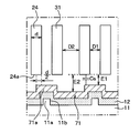
- FIG. 5 is a cross-sectional view of the sensor section along the line VV in FIG. 6 is an enlarged view of region A in FIG.
- FIG. 7 is a diagram illustrating a circuit configuration of the acceleration sensor.
- FIG. 8 (a) to 8 (g) are cross-sectional views showing manufacturing steps of the sensor unit shown in FIG.
- FIG. 9 is a plan view of a sensor unit of the acceleration sensor according to the second embodiment of the present disclosure.
- FIG. 10 is a cross-sectional view of the sensor unit and the cap unit along line XX in FIG.
- FIG. 11 is a plan view of a sensor unit of the acceleration sensor according to the third embodiment of the present disclosure.
- FIG. 12 is a cross-sectional view of the sensor unit and the cap unit along the line XII-XII in FIG.
- FIG. 13 is a cross-sectional view of the sensor unit and the cap unit of the acceleration sensor according to the fourth embodiment of the present disclosure.
- FIG. 9 is a plan view of a sensor unit of the acceleration sensor according to the second embodiment of the present disclosure.
- FIG. 10 is a cross-sectional view of the sensor unit and the cap unit along line XX in FIG.
- FIG. 11 is a plan view of
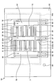
- FIG. 14 is a plan view of an acceleration sensor according to the fifth embodiment of the present disclosure.
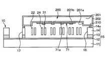
- FIG. 15 is a cross-sectional view of the sensor portion and the cap portion taken along line XV-XV in FIG.
- FIG. 16 is a diagram illustrating a circuit configuration of an acceleration sensor according to another embodiment of the present disclosure.
- FIG. 17 is a plan view of a sensor unit of an acceleration sensor according to another embodiment of the present disclosure.
- the acceleration sensor is a sensor unit configured using a substrate 15 in which a semiconductor layer 14 is disposed on a support substrate 11 via first and second insulating films 12 and 13. 10 is provided.
- the semiconductor layer 14 corresponds to the first substrate of the present disclosure
- the support substrate 11 corresponds to the second substrate of the present disclosure
- the support substrate 11 is a silicon substrate
- the first and second insulating films 12 and 13 are made of SiO 2 , SiN, or the like
- the semiconductor layer 14 is made of silicon, polysilicon, or the like.
- the movable portion 20 and the first and second fixed portions 30 and 40 are partitioned by the first groove portion 16 on the one surface 14 a side, and the connection portions 51 to 53 are partitioned by the second groove portion 17.
- a portion of the semiconductor layer 14 that is not partitioned by the first and second groove portions 16 and 17 is a peripheral portion 60.
- the one surface 14a of the semiconductor layer 14 is a surface opposite to the second insulating film 13 side, and the one surface 14a of the semiconductor layer 14 corresponds to one surface of the first substrate of the present disclosure.
- the movable part 20 is configured such that both ends in the longitudinal direction of the rectangular weight part 21 are integrally connected to the anchor parts 23 a and 23 b via the beam part 22.
- the anchor portions 23 a and 23 b are supported by the support substrate 11 through the first and second insulating films 12 and 13 in the first groove portion 16. Further, the portion of the second insulating film 13 that faces the movable portion 20 and the portions that face the first and second fixed electrodes 31 and 41 described later are removed to form the opening 18, and the movable portion 20 and the first The first and second fixed electrodes 31 and 41 are floating from the support substrate 11.
- the beam portion 22 has a rectangular frame shape in which two parallel beams are connected at both ends thereof, and has a spring function of being displaced in a direction perpendicular to the longitudinal direction of the two beams. Specifically, when the beam portion 22 receives an acceleration including a component in the longitudinal direction of the weight portion 21, the beam portion 22 is displaced in the longitudinal direction and restored to the original state in accordance with the disappearance of the acceleration. It has become. Therefore, the weight portion 21 connected to the support substrate 11 through such a beam portion 22 can be displaced in the displacement direction of the beam portion 22 (longitudinal direction of the weight portion 21) in accordance with the application of acceleration. .
- the movable portion 20 includes a plurality of movable electrodes 24 having a rectangular cross section formed integrally and projecting in opposite directions from both side surfaces of the weight portion 21 in a direction orthogonal to the longitudinal direction of the weight portion 21.
- movable electrodes 24 are formed on the left side and the right side of the weight part 21 so as to face the opening 18.
- Each movable electrode 24 is formed integrally with the weight portion 21 and the beam portion 22, and can be displaced in the longitudinal direction of the weight portion 21 together with the weight portion 21 when the beam portion 22 is displaced.
- the movable portion 20 is connected to the connection portion 51 via the movable portion wiring 25.
- the movable portion wiring 25 is made of a metal film such as polysilicon or aluminum, and a portion of the first insulating film 12 located immediately below the anchor portion 23a to a portion directly below the connecting portion 51. It is extended to.
- the anchor portion 23 a (movable portion 20) and the connection portion 51 are connected to the movable portion wiring 25 through a contact hole 13 a formed in the second insulating film 13.
- the first and second fixing portions 30 and 40 include first and second fixed electrodes 31 and 41 having a rectangular cross section, which are supported by the support substrate 11 via the first and second insulating films 12 and 13.
- the second support portions 32 and 42 are configured to be provided.
- the first and second fixed electrodes 31 and 41 have a predetermined detection interval with the side surface of the movable electrode 24, and the first and second fixed electrodes 31 and 41 have a comb-like shape so as to mesh with the comb-tooth gap in the movable electrode 24. It is supported by the second support parts 32 and 42 and faces the opening 18.
- first and second fixed electrodes 31 and 41 are arranged so that the displacement of the distance from the movable electrode 24 is opposite to each other when the movable portion 20 is displaced in the longitudinal direction of the weight portion 21. For example, when the distance between the movable electrode 24 and the first fixed electrode 31 is reduced when the movable electrode 24 is displaced, the distance between the movable electrode 24 and the second fixed electrode 41 is increased. .
- the first fixed electrode 31 is disposed on the upper side of the paper with respect to the movable electrode 24, and the second fixed electrode 41 is disposed on the lower side of the paper with respect to the movable electrode 24.
- the first and second fixing parts 30 and 40 are arranged so as to sandwich the weight part 21 therebetween.
- the first fixed unit 30 is disposed on the left side of the sheet with respect to the movable unit 20
- the second fixed unit 40 is disposed on the right side of the sheet with respect to the movable unit 20.
- the portion of the first insulating film 12 from which the second insulating film 13 is removed is opposed to only a part of the movable electrode 24, and the first and second elements constituting the capacitor Cs between the movable electrode 24 and the first insulating film 12.
- Two auxiliary electrodes 71a and 72a are formed (see FIG. 6).
- the first and second auxiliary electrodes 71 a and 72 a are constituted by a part of the first and second wiring portions 71 and 72 formed on the first insulating film 12.
- the support substrate 11 has a convex portion 11 a that protrudes in the normal direction of the one surface in the vicinity of the portion where the movable electrode 24 faces.
- the support substrate 11 has a recess 11b formed on one surface of the first insulating film 12 so that the protrusion 11a is formed.
- the convex part 11a may be formed in the part facing the movable electrode 24.
- the convex portion 11a in this embodiment, are formed first, include between the second fixed electrodes 31 and 41 constituting the capacitance C d between the movable electrode 24 and the movable electrode 24 .
- FIG. A second wiring portion 72 is formed in a portion of the first insulating film 12 that faces the movable electrode 24 and the second fixed electrode 41.
- the first and second wiring portions 71 and 72 are also formed on the wall surface including the protruding end surface of the convex portion 11a, and the distance between the portion formed on the protruding end surface and the movable electrode 24 is reduced.
- the convex portion 11 a is formed such that a part of the first and second wiring portions 71 and 72 is spaced from the movable electrode 24.
- the portion formed on the tip surface of the convex portion 11a via the first insulating film 12 is located on the bottom surface of the concave portion 11b via the first insulating film 12.
- the distance from the movable electrode 24 becomes narrower than the portion formed in this manner, and the capacitance becomes very large.
- the capacitor Cs is configured between the movable electrode 24 and a portion of the first and second wiring portions 71 and 72 where the distance from the movable electrode 24 is narrowed.
- portions of the first and second wiring portions 71 and 72 where the distance from the movable electrode 24 is narrowed become the first and second auxiliary electrodes 71a and 72a.
- the movable electrode 24 and the first fixed electrode 31 are arranged alternately (in a comb shape).
- the first auxiliary electrode 71 a is configured such that the surface of the movable electrode 24 on the side of the support substrate 11 is the lower surface 24 a when no acceleration is applied.
- the lower surface 24a of 24 it arrange
- the first auxiliary electrode 71a includes only a region on the first fixed electrode 31 side where the distance from the movable electrode 24 becomes narrow when the lower surface 24a is divided into two in a direction orthogonal to the displacement direction of the movable electrode 24.
- the movable electrode 24 has a first auxiliary electrode 71a that is d / 2 from the end on the first fixed electrode 31 side where the distance from the movable electrode 24 on the lower surface 24a becomes narrower. Is facing.
- the second auxiliary electrode 72a has the same configuration as the first auxiliary electrode 71a. That is, when the acceleration is not applied, the second auxiliary electrode 72a is a second fixed electrode whose interval with the movable electrode 24 is narrowed when the lower surface 24a is divided into two in a direction orthogonal to the displacement direction of the movable electrode 24. It is arranged so as to face only the region on the 41 side.
- the facing area between the movable electrode 24 facing the first fixed electrode 31 and the first auxiliary electrode 71a increases, and the second fixed electrode
- the opposing area of the movable electrode 24 facing the 41 and the second auxiliary electrode 72a decreases.
- the interval E1 between the movable electrode 24 and the first auxiliary electrode 71a is equal to the interval D1 between the movable electrode 24 and the first fixed electrode 31 where the interval between the movable electrode 24 becomes narrower.
- an interval E2 between the movable electrode 24 and the portion of the first wiring portion 71 that is different from the portion constituting the first auxiliary electrode 71a is the first fixed electrode 31 in which the interval between the movable electrode 24 and the movable electrode 24 is widened. Is equal to the distance D2.
- the part different from the part which comprises the 1st auxiliary electrode 71a among the 1st wiring parts 71 is the part formed in the bottom face of the recessed part 11b through the 1st insulating film 12 among the 1st wiring parts 71. It is.
- the distance E1 between the lower surface 24a of the movable electrode 24 and the second auxiliary electrode 72a is the distance D1 between the movable electrode 24 and the second fixed electrode 41 where the distance between the movable electrode 24 becomes narrower. Is equal to.
- a distance E2 between the movable electrode 24 and a portion of the second wiring portion 72 different from the second auxiliary electrode 72a is made equal to a distance D2 between the movable electrode 24 and the second fixed electrode 41. Yes.
- first and second wiring portions 71 and 72 pass through a portion of the first insulating film 12 facing the first support portion 32 and extend to a position directly below the connection portion 52.
- the second wiring portion 72 is formed to pass directly through the portion facing the second support portion 42 and directly below the connection portion 53.
- connection parts 52 and 53 are connected with the 1st, 2nd wiring parts 71 and 72 via the contact hole 13a formed in the 2nd insulating film 13, respectively.
- first and second support portions 32 and 42 are connected to the first and second wiring portions 71 and 72 via contact holes 13 a formed in the second insulating film 13, respectively. It is connected. That is, in the present embodiment, the first fixed electrode 31 and the first auxiliary electrode 71a (first wiring portion 71) are set to the same potential, and the second fixed electrode 41 and the second auxiliary electrode 72a (second wiring portion 72) Are at the same potential.
- pads 81 to 84 are formed in the connection portions 51 to 53 and the peripheral portion 60 of the semiconductor layer 14. Then, it is electrically connected to a circuit unit 100 (to be described later) via pads 81 to 84 via a wire or the like.
- the pad 84 formed in the peripheral portion 60 is applied with a predetermined potential from the circuit portion 100 in order to fix the potential of the peripheral portion 60.
- the sensor unit 10 is connected to the circuit unit 100, and the circuit unit 100 includes a CV conversion circuit 110 including an operational amplifier 101, a capacitor 102, and a switch 103. ing.
- the capacitor 102 and the switch 103 are arranged in parallel between the inverting input terminal and the output terminal of the operational amplifier 101.
- the first fixed electrode 31 and the first auxiliary electrode 71a are supplied with a pulse-shaped first carrier wave P1 having an amplitude between the voltages Vcc and 0V and having a predetermined frequency from the circuit unit 100. ing.
- the second fixed electrode 41 and the second auxiliary electrode 72a receive the second carrier wave P2 having the same amplitude and frequency as the first carrier wave P1 and having a phase difference of 180 ° from the circuit unit 100. Yes.
- C t1 in FIG. 7 is a capacitance formed between the movable electrode 24, the first fixed electrode 31 and the first auxiliary electrode 71a, and a capacitance between the movable electrode 24 and the first fixed electrode 31.
- C d and the movable electrode 24 is capacitance constituted by the sum of the capacitance C s between the first auxiliary electrode 71a.
- C t2 in FIG. 7 is a capacitance formed between the movable electrode 24, the second fixed electrode 41, and the second auxiliary electrode 72a, and is between the movable electrode 24 and the second fixed electrode 41.
- the capacitors C t1 and C t2 are expressed as follows.
- a support substrate 11 is prepared, and a concave portion 11b is formed by etching or the like to form a convex portion 11a.
- the first insulating film 12 is formed on the support substrate 11 by a chemical vapor deposition (CVD) method or the like.
- a polysilicon or a metal film is formed on the first insulating film 12 by a CVD method or the like. Then, by appropriately patterning using a mask or the like (not shown), the first wiring portion 71 is formed, and the movable portion wiring 25 and the second wiring portion 72 are formed in a cross section different from FIG. .
- the second insulating film 13 is formed by CVD or the like so as to cover the movable portion wiring 25 and the first and second wiring portions 71 and 72. Then, in a cross section different from FIG. 8 (d), as shown in FIGS. 3 and 4, the anchor portion 23a, the first and second support portions 32 and 42, and the connection portions 51 ⁇ in the second insulating film 13 are provided. A contact hole 13a is formed in a part of the portion where 53 is formed.
- a substrate 15 is formed by forming a semiconductor layer 14 on the second insulating film 13 by a CVD method or the like.
- the semiconductor layer 14 is embedded in the contact hole 13a as shown in FIG. 3 and FIG. 4 in a cross section different from FIG.
- aluminum or the like is vapor-deposited on the semiconductor layer 14 and patterned using a mask to form pads 81 to 84.
- the first groove 16 is formed in the semiconductor layer 14 using a mask (not shown) to form the movable portion 20 and the first and second fixed portions 30 and 40. To do. Further, in a cross section different from that shown in FIG. 8F, the second groove portion 17 is formed in the semiconductor layer 14 to form the connection portions 51 to 53.
- a predetermined region of the second insulating film 13 is removed, and the movable portion 20 and the first and second fixed electrodes 31 and 41 are replaced with the support substrate 11 (first insulating film 12). And the first and second auxiliary electrodes 71a and 72a are exposed. Thereby, the sensor unit 10 is formed.
- the first and second auxiliary electrodes 71a and 72a that change the facing area of the movable electrode 24 when the movable electrode 24 is displaced are provided. Then, the movable electrode 24 first, and the capacitance C d between the second fixed electrodes 31 and 41, the movable electrode 24 first, second auxiliary electrode 71a, on the basis of the capacitance C s between 72a Acceleration is detected. For this reason, detection sensitivity can be improved.
- the first and second auxiliary electrodes 71 a and 72 a are formed so as to face only a part of the movable electrode 24. For this reason, the amount of change in the facing area differs depending on the displacement direction of the movable electrode 24, and the displacement direction can be easily determined.
- first and second auxiliary electrodes 71a and 72a are regions on the first and second fixed electrodes 31 and 41 side in which the distance between the movable electrode 24 and the movable electrode 25 is narrow when no acceleration is applied. Are arranged to face each other. For this reason, when a certain acceleration is applied, the increase and decrease of the capacitance Cd and the capacitance Cs are in the same direction, and the combination with the circuit can be facilitated.
- the first and second auxiliary electrodes 71 a and 72 a have a distance from the movable electrode 24 when the lower surface 24 a is divided into two in a direction orthogonal to the displacement direction of the movable electrode 24.
- the first and second fixed electrodes 31 and 41 are arranged so as to face only the narrow regions. For this reason, even if the opposed area between the movable electrode 24 and the first and second auxiliary electrodes 71a and 72a is shifted due to a manufacturing error or the like by trying to manufacture the sensor unit 10 having such a configuration, the movable electrode 24 and the first and second auxiliary electrodes 71a and 72a can be prevented from being opposed to each other.
- a distance E1 between the movable electrode 24 and the first and second auxiliary electrodes 71a and 72a is a distance D1 between the movable electrode 24 and the first and second fixed electrodes 31 and 41 where the distance between the movable electrode 24 and the movable electrode 24 is reduced. Is equal to.
- an interval E2 between the movable electrode 24 and the first and second wiring portions 71 and 72 that are different from the portions constituting the first and second auxiliary electrodes 71a and 72a is the distance between the movable electrode 24 and the movable electrode 24. Is equal to the distance D2 between the first and second fixed electrodes 31, 41.
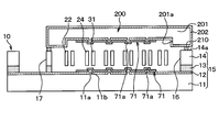
- the sensor unit 10 includes a cap unit 200, and the movable electrode 24, the first and second fixed electrodes 31, 41, and the first and second auxiliary electrodes 71a. 72a (first and second wiring portions 71, 72) are sealed.
- the cap unit 200 includes a bonded substrate 201 such as a silicon substrate, and the bonded substrate 201 includes a recess 201 a at a portion facing the movable electrode 24 and the first and second fixed electrodes 31 and 41. Is formed.
- An insulating film 202 is formed on the entire surface of the bonded substrate board 201. The insulating film 202 is also formed on the wall surface of the recess 201a.
- the cap part 200 is joined via the joining part 60a and the joining member 210 in the peripheral part 60 of the sensor part 10.
- the bonding member 210 is made of, for example, an oxide film, low dielectric glass, metal, or the like.
- the same effect as that of the first embodiment can be achieved while suppressing foreign matters from adhering to the movable electrode 24, the first and second fixed electrodes 31, 41, and the first and second auxiliary electrodes 71a, 72a. Can be obtained.
- the cap part 200 of the present embodiment has a convex part 201 b formed on the bottom surface of the concave part 201 a in the bonded substrate 201.
- a concave portion 201a is formed on the bonded substrate 201 so that the convex portion 201b is formed.
- first and second wiring portions 71 and 72 are formed in portions of the insulating film 202 facing the movable electrode 24 and the first and second fixed electrodes 31 and 41, and the first and second wiring portions 71 and 72 are formed.
- the first and second auxiliary electrodes 71a and 72a are formed in a portion where the distance from the movable electrode 24 becomes narrow. That is, the first and second auxiliary electrodes 71 a and 72 a formed on the support substrate 11 in the second embodiment via the first insulating film 12 are formed on the insulating film 202.
- the first and second auxiliary electrodes 71a and 72a of the present embodiment are the movable electrode 24, the first and second fixed electrodes 31 and 41, the first and second auxiliary electrodes 71a, which are described in the first embodiment. 72a is satisfied.
- the cap part 200 is formed with a through electrode part electrically connected to the first and second wiring parts 71 and 72 in a different cross-section from FIG. Then, the same voltage as that of the first fixed electrode 31 is applied to the first auxiliary electrode 71a and the same voltage as that of the second fixed electrode 41 is applied to the second auxiliary electrode 72a through the through electrode portion, as described above. It is to be applied.
- first and second fixing portion wirings 32a and 42a corresponding to the first and second wiring portions 71 and 72 are formed.
- the first and second support portions 32 and 42 are connected to the connection portions 52 and 53 via the first and second fixing portion wirings 32a and 42a, respectively.
- the first and second fixed portion wirings 32 a and 42 a do not constitute a capacitance with the movable electrode 24, but function to connect the first support portions 32 and 42 and the connection portions 52 and 53. It only fulfills.
- the substrate 15 corresponds to the first substrate of the present disclosure
- the bonded substrate 201 corresponds to the second substrate of the present disclosure.
- first and second auxiliary electrodes 71 a and 72 a are formed on the sensor unit 10 and the cap unit 200, respectively.
- the support substrate 11 and the bonded substrate 201 correspond to the second substrate of the present disclosure.
- the insulating film 12 and the semiconductor layer 14 are sequentially arranged on the support substrate 11 to constitute the substrate 15.
- a recess 19 is formed in a portion of the support substrate 11 and the insulating film 12 that faces the movable electrode 24 and the first and second fixed electrodes 31 and 41.
- the recess 19 is for preventing the movable electrode 24 and the first and second fixed electrodes 31 and 41 from coming into contact with the support substrate 11.
- the movable part 20 is arranged so as to cross over the hollow part 19, and both ends in the longitudinal direction of the weight part 21 are integrally connected to a rectangular frame-like frame part 26 via the beam part 22. Then, the anchor portion 23 located at the substantially central portion of the weight portion 21 is supported by the support substrate 11 via the insulating film 12 in the same manner as the first support portion 32 in FIG.
- the cap part 200 has a recessed part 201 a formed in a part of the bonded substrate 201 facing the movable electrode 24 and the first and second fixed electrodes 31, 41, and the anchor part 23, the first and second support parts 32. , 42 is not recessed.
- the first wiring portion 71 is formed in a portion facing the first support portion 32 in addition to a portion facing the movable electrode 24 and the first fixed electrode 31.
- the insulating film 202 has the second wiring portion 72 formed in the portion facing the second support portion 42 and the wiring portion formed in the portion facing the anchor portion 23. Has been.
- first and second wiring parts 71 and 72 and the wiring part are connected to the anchor part 23 and the first and second support parts 32 and 42, respectively. Further, the peripheral part 60 in the sensor part 10 is joined to the cap part 200 via the joining member 210.
- an insulating film 203 is formed on the side of the insulating film 202 opposite to the sensor unit 10 side.
- the cap portion 200 is formed with three through-electrode portions 204 that are electrically connected to the wiring portions connected to the first and second wiring portions 71 and 72 and the anchor portion 23 (in FIG. 15). Then only one is shown).
- the through electrode portion 204 has a through hole 204 a that penetrates the insulating film 203, the insulating film 202, and the bonded substrate 201 and reaches the first and second wiring portions 71 and 72.
- a through electrode 204c is embedded in the through hole 204a via an insulating film 204b, and a pad 204d that is electrically connected to the through electrode 204c is formed on the insulating film 203.
- the same effect as that of the third embodiment can also be obtained as an acceleration sensor using the sensor unit 10 and the cap unit 200.
- the first and second fixed electrodes 31 and 41 and the first and second auxiliary electrodes 71a and 72a may be electrically separated.
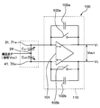
- the circuit unit 100 includes all of an operational amplifier 101, first and second capacitors 102a and 102b, and first and second switches 103a and 103b.
- a differential CV conversion circuit 110 may be provided.
- the first capacitor 102a and the first switch 103a are arranged in parallel between the inverting input terminal of the operational amplifier 101 and the + side output terminal.
- the second capacitor 102b and the second switch 103b are disposed in parallel between the non-inverting input terminal of the operational amplifier 101 and the negative output terminal.
- the operational amplifier 101 has an inverting input terminal connected to the first fixed electrode 31 and the first auxiliary electrode 71a, and a non-inverting input terminal connected to the second fixed electrode 41 and the second auxiliary electrode 72a.
- the movable part 20 is inputted with a pulse-shaped carrier wave P having an amplitude between the voltages Vcc and 0 V and having a predetermined frequency from the circuit part 100.
- the sensor signal V out (V1 ⁇ V2) may be output using the fully differential CV conversion circuit 110.
- the convex parts 11a and 201b do not need to be formed in the support substrate 11 or the bonded substrate board 201.
- FIG. 17 when the convex portion 11a is not formed on the support substrate 11, the first and second auxiliary electrodes 71a and 72a are formed so as to face a part of the movable electrode 24.
- the first and second auxiliary electrodes 71 a and 72 a adjacent to each other may be connected by the first and second wiring portions 71 and 72 in a different cross section from that of FIG.
- the support substrate 11 may be made of glass or the like.
- the acceleration sensor as the capacitive physical quantity sensor has been described as an example, but the present disclosure can be applied to an angular velocity sensor or a pressure sensor.
- the movable electrode 24, the first and second fixed electrodes 31, 41, the first and second auxiliary electrodes 71a and 72a satisfy the relationship of the distances D1, D2, E1 and E2 described in the first embodiment. It does not have to be. Even in such an acceleration sensor, the detection sensitivity can be improved by arranging the first and second auxiliary electrodes 71a and 72a.
Landscapes
- Engineering & Computer Science (AREA)
- Physics & Mathematics (AREA)
- General Physics & Mathematics (AREA)
- Manufacturing & Machinery (AREA)
- Microelectronics & Electronic Packaging (AREA)
- Pressure Sensors (AREA)
Abstract
容量式物理量センサは、第1基板(14、15)と、可動電極(24)と、固定電極(31、41)と、第2基板(11、201)と、を備える。前記第2基板のうち前記可動電極と対向する部分には、前記可動電極が所定方向における一方向に変位した場合と前記可動電極が前記一方向と反対方向に変位した場合とで前記可動電極との対向面積の変化量が異なる補助電極(71a、72a)が配置されており、前記可動電極と前記固定電極との間隔に応じた容量(Cd)および前記可動電極と前記補助電極との対向面積に応じた容量(Cs)に基づいて前記物理量を検出する。
Description
本開示は、2013年5月31日に出願された日本出願番号2013-115306号に基づくもので、ここにその記載内容を援用する。
本開示は、容量式物理量センサに関するものである。
従来より、物理量に応じて変化する容量をセンサ信号として出力する容量式物理量センサとして、例えば、加速度に応じたセンサ信号を出力する加速度センサが提案されている(例えば、特許文献1参照)。
具体的には、この加速度センサは、支持基板、絶縁膜、半導体層が順に積層されたSilicon on Insulator(SOI)基板を用いて構成されている。そして、半導体層に、加速度に応じて変位する可動電極と、可動電極と対向するように配置されることで可動電極との間に所定の容量を構成する固定電極が形成されている。
このような加速度センサでは、加速度が印加されると可動電極が加速度に応じて変位し、可動電極と固定電極との間隔が変化する。このため、可動電極と固定電極との間の容量に基づいて加速度の検出が行われる。
しかしながら、近年では、さらに検出感度を向上させたいという要望がある。なお、ここでは、容量式物理量センサとして、加速度センサを例に挙げて説明したが、例えば、角速度に応じて可動電極が変位する角速度センサにおいても同様の要望がある。
本開示は上記点に鑑みて、検出感度を向上できる容量式物理量センサを提供することを目的とする。
本開示の一態様に係る容量式物理量センサは、第1基板と、可動電極と、固定電極と、第2基板とを備える。前記第1基板は、一面を有する。前記可動電極は、前記第1基板の前記一面側に形成され、物理量が印加されることによって前記一面の面方向における所定方向に変位可能とされる。前記固定電極は、前記第1基板の前記一面側に前記可動電極と対向する状態で形成され、前記可動電極が変位することによって前記可動電極との間隔が変化する。前記第2基板は、前記第1基板と接合される。
前記第2基板のうち前記可動電極と対向する部分には、前記可動電極が前記所定方向における一方向に変位した場合と前記可動電極が前記一方向と反対方向に変位した場合とで前記可動電極との対向面積の変化量が異なる補助電極が配置されている。前記容量式物理量センサは、前記可動電極と前記固定電極との前記間隔に応じた容量および前記可動電極と前記補助電極との前記対向面積に応じた容量に基づいて前記物理量を検出する。
前記容量式物理量センサは、前記可動電極と前記固定電極との前記間隔に応じた前記容量および前記可動電極と前記補助電極との前記対向面積に応じた前記容量に基づいて前記物理量を検出しているため、検出感度を向上できる。また、前記補助電極は、前記可動電極が前記所定方向における前記一方向に変位した場合と前記反対方向に変位した場合とで前記可動電極との前記対向面積の変化量が異なるように配置されているため、前記可動電極の変位方向を容易に判定できる。
本開示における上記あるいは他の目的、構成、利点は、下記の図面を参照しながら、以下の詳細説明から、より明白となる。図面において、
図1は、本開示の第1実施形態における加速度センサのセンサ部の平面図である。
図2は、図1中のII-II線に沿ったセンサ部の断面図である。
図3は、図1中のIII-III線に沿ったセンサ部の断面図である。
図4は、図1中のIV-IV線に沿ったセンサ部の断面図である。
図5は、図1中のV-V線に沿ったセンサ部の断面図である。
図6は、図5中の領域Aの拡大図である。
図7は、加速度センサの回路構成を示す図である。
図8(a)~図8(g)は、図1に示すセンサ部の製造工程を示す断面図である。
図9は、本開示の第2実施形態における加速度センサのセンサ部の平面図である。
図10は、図9中のX-X線に沿ったセンサ部およびキャップ部の断面図である。
図11は、本開示の第3実施形態における加速度センサのセンサ部の平面図である。
図12は、図11中のXII-XII線に沿ったセンサ部およびキャップ部の断面図である。
図13は、本開示の第4実施形態における加速度センサのセンサ部およびキャップ部の断面図である。
図14は、本開示の第5実施形態における加速度センサの平面図である。
図15は、図14中のXV-XV線に沿ったセンサ部およびキャップ部の断面図である。
図16は、本開示の他の実施形態における加速度センサの回路構成を示す図である。
図17は、本開示の他の実施形態における加速度センサのセンサ部の平面図である。
以下、本開示の実施形態について図に基づいて説明する。なお、以下の各実施形態相互において、互いに同一もしくは均等である部分には、同一符号を付して説明を行う。
(第1実施形態)
本開示の第1実施形態について図面を参照しつつ説明する。なお、本実施形態では、容量式物理量センサとして、加速度に応じて容量が変化する容量式の加速度センサを例に挙げて説明する。
本開示の第1実施形態について図面を参照しつつ説明する。なお、本実施形態では、容量式物理量センサとして、加速度に応じて容量が変化する容量式の加速度センサを例に挙げて説明する。
図1~図5に示されるように、加速度センサは、支持基板11上に第1、第2絶縁膜12、13を介して半導体層14が配置された基板15を用いて構成されるセンサ部10を備えている。
なお、本実施形態では、半導体層14が本開示の第1基板に相当し、支持基板11が本開示の第2基板に相当している。また、支持基板11は、例えば、シリコン基板等が用いられ、第1、第2絶縁膜12、13はSiO2やSiN等が用いられ、半導体層14はシリコンやポリシリコン等が用いられる。
半導体層14には、一面14a側に第1溝部16によって可動部20および第1、第2固定部30、40が区画形成されていると共に、第2溝部17によって接続部51~53が区画形成されている。また、半導体層14のうち、第1、第2溝部16、17で区画されていない部分は、周辺部60とされている。なお、半導体層14の一面14aとは第2絶縁膜13側と反対側の面のことであり、当該半導体層14の一面14aが本開示の第1基板の一面に相当している。
可動部20は、矩形状の錘部21における長手方向の両端が梁部22を介してアンカー部23a、23bに一体に連結した構成とされている。
なお、アンカー部23a、23bは、第1溝部16内において、第1、第2絶縁膜12、13を介して支持基板11に支持されている。また、第2絶縁膜13のうち可動部20と対向する部分および後述する第1、第2固定電極31、41と対向する部分は除去されて開口部18とされており、可動部20および第1、第2固定電極31、41は支持基板11から浮遊した状態となっている。
梁部22は、平行な2本の梁がその両端で連結された矩形枠状とされており、2本の梁の長手方向と直交する方向に変位するバネ機能を有している。具体的には、梁部22は、錘部21の長手方向の成分を含む加速度を受けたとき、錘部21を長手方向へ変位させると共に、加速度の消失に応じて元の状態に復元させるようになっている。したがって、このような梁部22を介して支持基板11に連結された錘部21は、加速度の印加に応じて梁部22の変位方向(錘部21の長手方向)へ変位可能となっている。
また、可動部20は、錘部21の長手方向と直交した方向に、錘部21の両側面から互いに反対方向へ一体的に突出形成された断面矩形状の可動電極24を複数備えている。図1では、可動電極24は、錘部21の左側および右側にそれぞれ4個ずつ突出して形成されており、開口部18に臨んだ状態となっている。また、各可動電極24は、錘部21および梁部22と一体的に形成されており、梁部22が変位することによって錘部21と共に錘部21の長手方向に変位可能となっている。
そして、可動部20は、可動部用配線25を介して接続部51と接続されている。具体的には、可動部用配線25は、ポリシリコンやアルミニウム等の金属膜で構成され、第1絶縁膜12のうちアンカー部23aの直下に位置する部分から接続部51の直下に位置する部分まで延設されている。そして、アンカー部23a(可動部20)および接続部51は、第2絶縁膜13に形成されたコンタクトホール13aを介して可動部用配線25と接続されている。
第1、第2固定部30、40は、断面矩形状の第1、第2固定電極31、41が第1、第2絶縁膜12、13を介して支持基板11に支持された第1、第2支持部32、42に備えられた構成とされている。具体的には、第1、第2固定電極31、41は、可動電極24の側面と所定の検出間隔を有し、可動電極24における櫛歯の隙間に噛み合うように櫛歯状に第1、第2支持部32、42に支持され、開口部18に臨んだ状態となっている。
なお、加速度が印加されていない場合には、可動電極24と第1、第2固定電極31、41との間隔が等しくされている。このため、図1中にコンデンサ記号で示す様に、可動電極24と第1、第2固定電極31、41との間には、それぞれ容量Cdが構成される。
また、第1、第2固定電極31、41は、可動部20が錘部21の長手方向に変位したとき、可動電極24との間隔の変位が互いに逆となるように配置されている。例えば、可動電極24が変位したとき、可動電極24と第1固定電極31との間隔が狭くなる場合には、可動電極24と第2固定電極41との間隔が広くなるように形成されている。図1では、第1固定電極31は、可動電極24に対して紙面上側に配置され、第2固定電極41は、可動電極24に対して紙面下側に配置されている。
そして、第1、第2固定部30、40は、錘部21を挟むように配置されている。図1では、第1固定部30が可動部20に対して紙面左側に配置され、第2固定部40が可動部20に対して紙面右側に配置されている。
また、第1絶縁膜12のうち第2絶縁膜13が除去された部分には、可動電極24の一部のみと対向し、可動電極24との間に容量Csを構成する第1、第2補助電極71a、72aが形成されている(図6参照)。この第1、第2補助電極71a、72aは、第1絶縁膜12上に形成された第1、第2配線部71、72の一部で構成されている。以下に、本実施形態の第1、第2補助電極71a、72aの構成について具体的に説明する。
支持基板11には、可動電極24の対向する部分の近傍に当該一面の法線方向に突出する凸部11aが形成されている。言い換えると、支持基板11には、第1絶縁膜12側の一面に、当該凸部11aが形成されるように凹部11bが形成されている。
なお、凸部11aは、可動電極24と対向する部分に形成されていてもよい。また、凸部11aは、本実施形態では、可動電極24と当該可動電極24との間に容量Cdを構成する第1、第2固定電極31、41との間を含んで形成されている。
そして、第1絶縁膜12のうち可動電極24および第1固定電極31と対向する部分に第1配線部71が形成されている。また、第1絶縁膜12のうち可動電極24および第2固定電極41と対向する部分に第2配線部72が形成されている。なお、これら第1、第2配線部71、72は、凸部11aの突出方向先端面を含む壁面にも形成され、突出方向先端面に形成された部分が可動電極24との間隔が狭くなる。言い換えると、凸部11aは、第1、第2配線部71、72の一部が可動電極24との間隔が狭くなるように形成されている。
ここで、第1、第2配線部71、72のうち凸部11aの先端面に第1絶縁膜12を介して形成されている部分の方が凹部11bの底面に第1絶縁膜12を介して形成されている部分よりも可動電極24との間隔が狭くなって容量が非常に大きくなる。このため、容量Csは、第1、第2配線部71、72のうち可動電極24との間隔が狭くなる部分と当該可動電極24との間で構成されているといえる。本実施形態では第1、第2配線部71、72のうち可動電極24との間隔が狭くなる部分が第1、第2補助電極71a、72aとなる。
また、上記のように、可動電極24と第1固定電極31とは交互(櫛歯状)に配置されている。そして、本実施形態では、図6に示されるように、第1補助電極71aは、加速度が印加されていない場合において、可動電極24における支持基板11側の面を下面24aとしたとき、可動電極24の下面24aのうち当該可動電極24との間隔が狭くなる第1固定電極31側に配置されている。具体的には、第1補助電極71aは、下面24aを可動電極24の変位方向と直交する方向に2分割したとき、可動電極24との間隔が狭くなる第1固定電極31側の領域のみと対向するように配置されている。言い換えると、可動電極24は、可動電極24の幅をdとしたとき、下面24aにおける可動電極24との間隔が狭くなる第1固定電極31側の端部からd/2だけ第1補助電極71aと対向している。
なお、特に図示しないが、第2補助電極72aも第1補助電極71aと同様の構成とされている。すなわち、第2補助電極72aは、加速度が印加されていない場合において、下面24aを可動電極24の変位方向と直交する方向に2分割したとき、可動電極24との間隔が狭くなる第2固定電極41側の領域のみと対向するように配置されている。
例えば、可動電極24が図1中紙面上側(アンカー部23b側)に変位すると、第1固定電極31と対向する可動電極24と第1補助電極71aとの対向面積は増加し、第2固定電極41と対向する可動電極24と第2補助電極72aとの対向面積は減少する。
また、可動電極24と第1補助電極71aとの間隔E1は、可動電極24と当該可動電極24との間隔が狭くなる第1固定電極31との間隔D1と等しくされている。また、可動電極24と第1配線部71のうち第1補助電極71aを構成する部分と異なる部分との間隔E2は、可動電極24と当該可動電極24との間隔が広くなる第1固定電極31との間隔D2と等しくされている。
なお、第1配線部71のうち第1補助電極71aを構成する部分と異なる部分とは、第1配線部71のうち凹部11bの底面に第1絶縁膜12を介して形成された部分のことである。また、特に図示していないが、可動電極24の下面24aと第2補助電極72aとの間隔E1は、可動電極24と当該可動電極24との間隔が狭くなる第2固定電極41との間隔D1と等しくされている。そして、第2配線部72のうち第2補助電極72aと異なる部分と可動電極24との間隔E2は、当該可動電極24との間隔が広くなる第2固定電極41との間隔D2と等しくされている。
また、図1に示されるように、第1、第2配線部71、72は、第1絶縁膜12のうち第1支持部32と対向する部分を通過して接続部52の直下まで延設されている。第2配線部72は、第2支持部42と対向する部分を通過して接続部53の直下まで形成されている。
そして、図4に示されるように、接続部52、53は、それぞれ第2絶縁膜13に形成されたコンタクトホール13aを介して第1、第2配線部71、72と接続されている。同様に、図3に示されるように、第1、第2支持部32、42は、それぞれ第2絶縁膜13に形成されたコンタクトホール13aを介して第1、第2配線部71、72と接続されている。つまり、本実施形態では、第1固定電極31と第1補助電極71a(第1配線部71)が同電位とされ、第2固定電極41と第2補助電極72a(第2配線部72)とが同電位とされる。
また、図4に示されるように、半導体層14のうち接続部51~53および周辺部60には、パッド81~84が形成されている。そして、パッド81~84を介して後述する回路部100とワイヤ等を介して電気的に接続されるようになっている。なお、周辺部60に形成されたパッド84は、周辺部60の電位を固定するために回路部100から所定の電位が印加されるものである。
次に、加速度センサの回路構成について図7を参照しつつ説明する。図7に示されるように、センサ部10は、回路部100と接続されており、回路部100には、演算増幅器101、コンデンサ102、スイッチ103によって構成されるC-V変換回路110が備えられている。
具体的には、コンデンサ102およびスイッチ103は、演算増幅器101の反転入力端子と出力端子との間に並列的に配置されている。そして、演算増幅器101は、反転入力端子が可動電極24と接続され、非反転入力端子にVcc/2(例えば、Vcc=5V)の電圧が入力されるようになっている。
また、第1固定電極31および第1補助電極71aには、回路部100から電圧Vccと0Vとの間で振幅し、所定の周波数を有するパルス状の第1搬送波P1が入力されるようになっている。そして、第2固定電極41および第2補助電極72aには、回路部100から第1搬送波P1と振幅および周波数が同じであり、位相が180°異なる第2搬送波P2が入力されるようになっている。
なお、図7中のCt1は、可動電極24と第1固定電極31および第1補助電極71aとの間に構成される容量であり、可動電極24および第1固定電極31との間の容量Cdと可動電極24と第1補助電極71aとの間の容量Csとの和で構成される容量である。同様に、図7中のCt2は、可動電極24と第2固定電極41および第2補助電極72aとの間に構成される容量であり、可動電極24および第2固定電極41との間の容量Cdと可動電極24と第2補助電極72aとの間の容量Csとの和で構成される容量である。また、このような回路部100では、スイッチ103がオフされているときに加速度の検出が行われ、スイッチ103がオン(閉)されているときにコンデンサ102のリセットが行われる。
そして、例えば、図1中紙面上側に向かう方向の加速度が印加されると、可動電極24と第1固定電極31との間隔が狭くなると共に可動電極24と第1補助電極71aとの対向面積が増加する。これに対し、可動電極24と第2固定電極41との間隔は広くなると共に可動電極24と第2補助電極72aとの対向面積が減少する。このため、容量Ct1、Ct2は次のように示される。
(数1)Ct1=Cd+ΔCd+Cs+ΔCs
(数2)Ct2=Cd-ΔCd+Cs-ΔCs
なお、Cd、Csは初期容量であり、ΔCd、ΔCsは加速度に依存する加速度項である。したがって、演算増幅器101から出力されるセンサ信号Voutは、コンデンサ102の容量をCfとすると、次式で示される。
(数2)Ct2=Cd-ΔCd+Cs-ΔCs
なお、Cd、Csは初期容量であり、ΔCd、ΔCsは加速度に依存する加速度項である。したがって、演算増幅器101から出力されるセンサ信号Voutは、コンデンサ102の容量をCfとすると、次式で示される。
(数3)Vout=(Ct1-Ct2)・Vcc/Cf
=(2ΔCd+2ΔCs)・Vcc/Cf
次に、上記センサ部10の製造方法について図8(a)~図8(g)を参照して簡単に説明する。なお、図8(a)~図8(g)は、図1中のV-V線に沿った断面図である。
=(2ΔCd+2ΔCs)・Vcc/Cf
次に、上記センサ部10の製造方法について図8(a)~図8(g)を参照して簡単に説明する。なお、図8(a)~図8(g)は、図1中のV-V線に沿った断面図である。
まず、図8(a)に示されるように、支持基板11を用意し、エッチング等によって凹部11bを形成して凸部11aを形成する。そして、図8(b)に示されるように、支持基板11上にChemical Vapor Deposition(CVD)法等によって第1絶縁膜12を形成する。
続いて、図8(c)に示されるように、第1絶縁膜12上にCVD法等によってポリシリコンや金属膜等を形成する。そして、図示しないマスク等を用いて適宜パターニングすることにより、第1配線部71を形成すると共に、図8(c)とは別断面において、可動部用配線25および第2配線部72を形成する。
その後、図8(d)に示されるように、可動部用配線25、第1、第2配線部71、72を覆うように、CVD法等によって第2絶縁膜13を形成する。そして、図8(d)とは別断面において、図3および図4に示されるように、第2絶縁膜13のうちアンカー部23a、第1、第2支持部32、42、接続部51~53が形成される部分の一部にコンタクトホール13aを形成する。
続いて、図8(e)に示されるように、第2絶縁膜13上にCVD法等で半導体層14を形成することにより、基板15を構成する。なお、このとき、図8(e)とは別断面において、図3および図4に示されるように、コンタクトホール13a内に半導体層14が埋め込まれる。そして、図8(e)とは別断面において、図4に示されるように、半導体層14上にアルミニウム等を蒸着し、マスクを用いてパターニングすることにより、パッド81~84を形成する。
次に、図8(f)に示されるように、図示しないマスクを用いて、半導体層14に第1溝部16を形成して可動部20および第1、第2固定部30、40を区画形成する。また、図8(f)とは別断面において、半導体層14に第2溝部17を形成して接続部51~53を区画形成する。
その後、図8(g)に示されるように、第2絶縁膜13の所定領域を除去して可動部20および第1、第2固定電極31、41を支持基板11(第1絶縁膜12)からリリースすると共に第1、第2補助電極71a、72aを露出させる。これにより、上記センサ部10が形成される。
以上説明したように、本実施形態では、可動電極24が変位すると当該可動電極24との対向面積が変化する第1、第2補助電極71a、72aを備えている。そして、可動電極24と第1、第2固定電極31、41との間の容量Cdと、可動電極24と第1、第2補助電極71a、72aとの間の容量Csとに基づいて加速度を検出している。このため、検出感度を向上できる。
また、第1、第2補助電極71a、72aは、可動電極24の一部のみと対向するように形成されている。このため、可動電極24の変位方向によって対向面積の変化量が異なり、変位方向を容易に判定できる。
さらに、第1、第2補助電極71a、72aは、加速度が印加されていない場合において、可動電極24のうち当該可動電極25との間隔が狭い第1、第2固定電極31、41側の領域と対向するように配置されている。このため、ある加速度が印加された場合の容量Cdと容量Csの増減が同じ向きとなり、回路との組み合わせを容易にできる。
そして、第1、第2補助電極71a、72aは、加速度が印加されていない場合において、下面24aを可動電極24の変位方向と直交する方向に2分割したとき、当該可動電極24との間隔が狭い第1、第2固定電極31、41側の領域のみと対向するように配置されている。このため、このような構成のセンサ部10を製造しようとすることにより、仮に製造誤差等によって可動電極24と第1、第2補助電極71a、72aとの対向面積がずれたとしても、可動電極24と第1、第2補助電極71a、72aとが対向しなくなることを抑制できる。
さらに、可動電極24と第1、第2補助電極71a、72aとの間隔E1は、可動電極24と当該可動電極24との間隔が狭くなる第1、第2固定電極31、41との間隔D1と等しくされている。また、可動電極24と第1、第2配線部71、72のうち第1、第2補助電極71a、72aを構成する部分と異なる部分との間隔E2は、可動電極24と当該可動電極24との間隔が広くなる第1、第2固定電極31、41との間隔D2と等しくされている。
このため、可動電極24と第1、第2補助電極71a、72aとの間、および可動電極24と当該可動電極24との間隔が狭くなる第1、第2固定電極31、41との間のコンデンサとしてのノイズを等しくできる。また、可動電極24と第1、第2配線部71、72のうち第1、第2補助電極71a、72aを構成する部分と異なる部分との間、および可動電極24と当該可動電極24との間隔が広くなる第1、第2固定電極31、41との間のコンデンサとしてのノイズを等しくできる。このため、センサ信号Voutを所定のノイズフィルタで処理することにより、コンデンサとしてのノイズを容易に除去でき、さらに検出感度を向上できる。
(第2実施形態)
本開示の第2実施形態について説明する。本実施形態は、第1実施形態に対してキャップ部を備えたものであり、その他に関しては第1実施形態と同様であるため、ここでは説明を省略する。
本開示の第2実施形態について説明する。本実施形態は、第1実施形態に対してキャップ部を備えたものであり、その他に関しては第1実施形態と同様であるため、ここでは説明を省略する。
図9および図10に示されるように、本実施形態では、センサ部10にキャップ部200が備えられ、可動電極24、第1、第2固定電極31、41および第1、第2補助電極71a、72a(第1、第2配線部71、72)が封止されている。
具体的には、キャップ部200は、シリコン基板等の貼り合わせ基板201を有し、貼り合わせ基板201には、可動電極24および第1、第2固定電極31、41と対向する部分に凹部201aが形成されている。そして、貼り合わせ基板201の表面全面に絶縁膜202が形成されている。なお、絶縁膜202は、凹部201aの壁面にも形成されている。
そして、キャップ部200は、センサ部10の周辺部60における接合部60aと接合部材210を介して接合されている。なお、接合部材210は、例えば、酸化膜や低誘電ガラス、金属等が用いられる。
これによれば、可動電極24、第1、第2固定電極31、41および第1、第2補助電極71a、72aに異物が付着することを抑制しつつ、上記第1実施形態と同様の効果を得ることができる。
(第3実施形態)
本開示の第3実施形態について説明する。本実施形態は、第2実施形態に対して第1、第2配線部71、72をキャップ部200に形成したものであり、その他に関しては第2実施形態と同様であるため、ここでは説明を省略する。
本開示の第3実施形態について説明する。本実施形態は、第2実施形態に対して第1、第2配線部71、72をキャップ部200に形成したものであり、その他に関しては第2実施形態と同様であるため、ここでは説明を省略する。
図11および図12に示されるように、本実施形態のキャップ部200は、貼り合わせ基板201のうち凹部201aの底面に凸部201bが形成されている。言い換えると、貼り合わせ基板201には、当該凸部201bが形成されるように凹部201aが形成されている。
そして、絶縁膜202のうち可動電極24および第1、第2固定電極31、41と対向する部分に第1、第2配線部71、72が形成され、第1、第2配線部71、72のうち可動電極24との間隔が狭くなる部分で第1、第2補助電極71a、72aが構成される。すなわち、上記第2実施形態における支持基板11に第1絶縁膜12を介して形成された第1、第2補助電極71a、72aが絶縁膜202上に形成されている。
なお、本実施形態の第1、第2補助電極71a、72aは、上記第1実施形態で説明した可動電極24、第1、第2固定電極31、41、第1、第2補助電極71a、72aの関係を満たすように形成されている。
また、キャップ部200には、図12とは異なる別断面において、第1、第2配線部71、72と電気的に接続される貫通電極部が形成されている。そして、当該貫通電極部を介して、上記と同様に、第1補助電極71aに第1固定電極31と同じ電圧が印加されると共に、第2補助電極72aに第2固定電極41と同じ電圧が印加されるようになっている。
さらに、第1絶縁膜12上には、上記第1、第2配線部71、72に相当する第1、第2固定部用配線32a、42aが形成されている。そして、第1、第2支持部32、42は、当該第1、第2固定部用配線32a、42aを介してそれぞれ接続部52、53に接続されている。
なお、この第1、第2固定部用配線32a、42aは、可動電極24との間に容量を構成するものではなく、第1支持部32、42と接続部52、53とを接続する機能のみを果すものである。また、本実施形態では、基板15が本開示の第1基板に相当し、貼り合わせ基板201が本開示の第2基板に相当している。
このようにキャップ部200に第1、第2補助電極71a、72aを形成しても、上記第2実施形態と同様の効果を得ることができる。
(第4実施形態)
本開示の第4実施形態について説明する。本実施形態は、第2実施形態と第3実施形態とを組み合わせたものであり、その他に関しては第2実施形態と同様であるため、ここでは説明を省略する。
本開示の第4実施形態について説明する。本実施形態は、第2実施形態と第3実施形態とを組み合わせたものであり、その他に関しては第2実施形態と同様であるため、ここでは説明を省略する。
図13に示されるように、本実施形態では、センサ部10およびキャップ部200にそれぞれ第1、第2補助電極71a、72aが形成されている。なお、本実施形態では、支持基板11および貼り合わせ基板201が本開示の第2基板に相当している。
これによれば、さらに感度を向上しつつ、上記第2実施形態と同様の効果を得ることができる。
(第5実施形態)
本開示の第5実施形態について説明する。本実施形態は、第3実施形態に対してセンサ部10およびキャップ部200の構造を変更したものであり、その他に関しては第3実施形態と同様であるため、ここでは説明を省略する。
本開示の第5実施形態について説明する。本実施形態は、第3実施形態に対してセンサ部10およびキャップ部200の構造を変更したものであり、その他に関しては第3実施形態と同様であるため、ここでは説明を省略する。
図14および図15に示されるように、本実施形態では、支持基板11上に絶縁膜12、半導体層14が順に配置されて基板15が構成されている。そして、支持基板11および絶縁膜12のうち可動電極24および第1、第2固定電極31、41と対向する部分には、窪み部19が形成されている。なお、この窪み部19は、可動電極24および第1、第2固定電極31、41が支持基板11と接触することを防止するためのものである。
可動部20は、窪み部19上を横断するように配置され、錘部21における長手方向の両端が梁部22を介して矩形枠状の枠部26に一体に連結した構成とされている。そして、錘部21の略中央部に位置するアンカー部23にて、図14中の第1支持部32と同様に、絶縁膜12を介して支持基板11に支持されている。
キャップ部200は、貼り合わせ基板201のうち可動電極24および第1、第2固定電極31、41と対向する部分に凹部201aが形成されており、アンカー部23、第1、第2支持部32、42と対向する部分は凹んでいない。
また、絶縁膜202には、可動電極24および第1固定電極31と対向する部分に加えて第1支持部32と対向する部分にも第1配線部71が形成されている。なお、図15とは別断面において、絶縁膜202には、第2支持部42と対向する部分にも第2配線部72が形成されていると共にアンカー部23と対向する部分に配線部が形成されている。
そして、第1、第2配線部71、72の一部および配線部がそれぞれアンカー部23、第1、第2支持部32、42と接続されている。また、センサ部10における周辺部60は、接合部材210を介してキャップ部200と接合されている。
さらに、絶縁膜202のうちセンサ部10側と反対側には、絶縁膜203が形成されている。そして、キャップ部200には、第1、第2配線部71、72およびアンカー部23と接続される配線部と電気的に接続される3つの貫通電極部204が形成されている(図15中では1つのみ図示)。
具体的には、この貫通電極部204は、絶縁膜203、絶縁膜202、貼り合わせ基板201を貫通して第1、第2配線部71、72に達する貫通孔204aを有している。そして、当該貫通孔204aに絶縁膜204bを介して貫通電極204cが埋め込まれ、絶縁膜203上に貫通電極204cと電気的に接続されるパッド204dが形成された構成とされている。
このようなセンサ部10およびキャップ部200を用いた加速度センサとしても、上記第3実施形態と同様の効果を得ることができる。
(他の実施形態)
本開示は上記した実施形態に限定されるものではなく、特許請求の範囲に記載した範囲内において適宜変更が可能である。
本開示は上記した実施形態に限定されるものではなく、特許請求の範囲に記載した範囲内において適宜変更が可能である。
例えば、上記各実施形態において、第1、第2固定電極31、41と第1、第2補助電極71a、72aとが電気的に分離されていてもよい。
また、上記各実施形態において、回路部100には、図16に示されるように、演算増幅器101、第1、第2コンデンサ102a、102b、第1、第2スイッチ103a、103bによって構成される全差動型のC-V変換回路110が備えられていてもよい。この場合、第1コンデンサ102aおよび第1スイッチ103aは、演算増幅器101の反転入力端子と+側の出力端子との間に並列的に配置される。また、第2コンデンサ102bおよび第2スイッチ103bは、演算増幅器101の非反転入力端子と-側の出力端子との間に並列的に配置される。そして、演算増幅器101は、反転入力端子が第1固定電極31および第1補助電極71aと接続され、非反転入力端子が第2固定電極41および第2補助電極72aと接続される。
また、可動部20には、回路部100から電圧Vccと0Vとの間で振幅し、所定の周波数を有するパルス状の搬送波Pが入力されるようになっている。
このように、全差動型のC-V変換回路110を用いてセンサ信号Vout(V1-V2)を出力するようにしてもよい。
さらに、上記各実施形態において、支持基板11または貼り合わせ基板201に凸部11a、201bが形成されていなくてもよい。例えば、図17に示されるように、支持基板11に凸部11aを形成しない場合には、可動電極24の一部と対向するように第1、第2補助電極71a、72aを形成し、図17とは異なる別断面において、隣接する第1、第2補助電極71a、72a同士を第1、第2配線部71、72で連結すればよい。
また、上記各実施形態において、支持基板11をガラス等で構成してもよい。
そして、上記各実施形態では、容量式物理量センサとしての加速度センサを例に挙げて説明したが、角速度センサや圧力センサに本開示を適用することも可能である。
さらに、可動電極24、第1、第2固定電極31、41、第1、第2補助電極71a、72aは、上記第1実施形態で説明した間隔D1、D2、E1、E2の関係を満たしていなくてもよい。このような加速度センサであっても、第1、第2補助電極71a、72aが配置されていることにより、検出感度を向上できる。
Claims (9)
- 一面(14a)を有する第1基板(14、15)と、
前記第1基板の前記一面側に形成され、物理量が印加されることによって前記一面の面方向における所定方向に変位可能とされた可動電極(24)と、
前記第1基板の前記一面側に前記可動電極と対向する状態で形成され、前記可動電極が変位することによって前記可動電極との間隔が変化する固定電極(31、41)と、
前記第1基板と接合される第2基板(11、201)と、を備え、
前記第2基板のうち前記可動電極と対向する部分には、前記可動電極が前記所定方向における一方向に変位した場合と前記可動電極が前記一方向と反対方向に変位した場合とで前記可動電極との対向面積の変化量が異なる補助電極(71a、72a)が配置されており、
前記可動電極と前記固定電極との前記間隔に応じた容量(Cd)および前記可動電極と前記補助電極との前記対向面積に応じた容量(Cs)に基づいて前記物理量を検出する容量式物理量センサ。 - 前記補助電極は、前記可動電極の一部のみと対向する状態で配置されている請求項1に記載の容量式物理量センサ。
- 前記第2基板(11)は、前記第1基板(14)の前記一面と反対側の他面に配置されて前記第1基板を支持している請求項1または2に記載の容量式物理量センサ。
- 前記第1基板(15)は、支持基板(11)上に絶縁膜(12、13)および半導体層(14)が順に配置された基板であり、
前記第2基板(201)は、前記第1基板の前記一面側に配置されて前記可動電極、前記固定電極、前記補助電極を封止する請求項1または2に記載の容量式物理量センサ。 - 前記支持基板および前記半導体層は、シリコンで構成されている請求項4に記載の容量式物理量センサ。
- 前記第2基板は2つ設けられ、
一方の前記第2基板は、前記第1基板の前記一面側に配置されて前記可動電極、前記固定電極、前記補助電極を封止し、他方の前記第2基板は、前記第1基板の前記一面と反対側に配置されて前記第1基板を支持しており、
前記補助電極は、それぞれの前記第2基板に配置されている請求項1または2に記載の容量式物理量センサ。 - 前記可動電極は、前記可動電極の変位方向に沿った断面が前記第2基板と対向する一面(24a)を有する矩形状とされ、当該一面を前記可動電極の変位方向と直交する方向に2分割したとき、一方の領域のみが前記補助電極と対向している請求項1ないし6のいずれか1つに記載の容量式物理量センサ。
- 前記可動電極および前記固定電極は、交互に複数配置されており、
前記第2基板には、前記可動電極および前記固定電極と対向する部分に配線部(71、72)が形成されていると共に、前記配線部と前記可動電極との間隔を狭くする凸部(11a、201b)が形成され、
前記補助電極は、前記配線部のうち前記可動電極との間隔が狭くなる部分で構成され、
前記補助電極と前記可動電極との間隔(E1)は、前記可動電極と前記固定電極との間隔(D1)と等しくされており、
前記配線部のうち前記補助電極を構成する部分と異なる部分と前記可動電極との間隔(E2)は、前記可動電極と当該可動電極を挟んで配置された前記固定電極のうち前記可動電極との間隔が広くされた前記固定電極との間隔(D2)と等しくされている請求項1ないし7のいずれか1つに記載の容量式物理量センサ。 - 前記固定電極は、前記可動電極が前記所定方向における一方向に変位したとき、前記可動電極との間隔が狭くなる第1固定電極(31)と、前記可動電極との間隔が広くなる第2固定電極(41)とを有し、
前記補助電極は、前記可動電極が前記所定方向における一方向に変位したとき、前記可動電極との対向面積が広くなる第1補助電極(71a)と、前記可動電極との対向面積が小さくなる第2補助電極(72a)とを有し、
前記可動電極と前記第1固定電極との間の容量と前記可動電極と前記第1補助電極との間の容量の和(Ct1)と、前記可動電極と前記第2固定電極との間の容量と前記可動電極と第2補助電極との間の容量の和(Ct2)との差に基づいたセンサ信号を出力する請求項1ないし8のいずれか1つに記載の容量式物理量センサ。
Priority Applications (1)
| Application Number | Priority Date | Filing Date | Title |
|---|---|---|---|
| US14/890,642 US9823266B2 (en) | 2013-05-31 | 2014-05-16 | Capacitive physical quantity sensor |
Applications Claiming Priority (2)
| Application Number | Priority Date | Filing Date | Title |
|---|---|---|---|
| JP2013-115306 | 2013-05-31 | ||
| JP2013115306A JP5967018B2 (ja) | 2013-05-31 | 2013-05-31 | 容量式物理量センサ |
Publications (1)
| Publication Number | Publication Date |
|---|---|
| WO2014192242A1 true WO2014192242A1 (ja) | 2014-12-04 |
Family
ID=51988296
Family Applications (1)
| Application Number | Title | Priority Date | Filing Date |
|---|---|---|---|
| PCT/JP2014/002594 Ceased WO2014192242A1 (ja) | 2013-05-31 | 2014-05-16 | 容量式物理量センサ |
Country Status (3)
| Country | Link |
|---|---|
| US (1) | US9823266B2 (ja) |
| JP (1) | JP5967018B2 (ja) |
| WO (1) | WO2014192242A1 (ja) |
Cited By (1)
| Publication number | Priority date | Publication date | Assignee | Title |
|---|---|---|---|---|
| CN108663541A (zh) * | 2017-03-27 | 2018-10-16 | 精工爱普生株式会社 | 物理量传感器、电子设备、便携式电子设备以及移动体 |
Families Citing this family (4)
| Publication number | Priority date | Publication date | Assignee | Title |
|---|---|---|---|---|
| JP6123613B2 (ja) * | 2013-09-26 | 2017-05-10 | 株式会社デンソー | 物理量センサおよびその製造方法 |
| JP6433842B2 (ja) | 2015-04-03 | 2018-12-05 | 株式会社東芝 | 電子装置及びその製造方法 |
| CN105675921B (zh) * | 2016-01-18 | 2018-10-26 | 广东合微集成电路技术有限公司 | 一种加速度传感器及其制作方法 |
| US11279614B2 (en) * | 2019-06-28 | 2022-03-22 | Analog Devices, Inc. | Low-parasitic capacitance MEMS inertial sensors and related methods |
Citations (4)
| Publication number | Priority date | Publication date | Assignee | Title |
|---|---|---|---|---|
| JP2011169889A (ja) * | 2010-02-19 | 2011-09-01 | Honeywell Internatl Inc | 面外櫛形駆動の加速度計 |
| JP2012177563A (ja) * | 2011-02-25 | 2012-09-13 | Seiko Epson Corp | 物理量センサー、および電子機器 |
| JP2012194112A (ja) * | 2011-03-17 | 2012-10-11 | Hitachi Automotive Systems Ltd | 半導体物理量検出センサ |
| JP2012202696A (ja) * | 2011-03-23 | 2012-10-22 | Asahi Kasei Electronics Co Ltd | 静電容量型加速度センサ |
Family Cites Families (10)
| Publication number | Priority date | Publication date | Assignee | Title |
|---|---|---|---|---|
| JP3307328B2 (ja) | 1998-05-11 | 2002-07-24 | 株式会社デンソー | 半導体力学量センサ |
| JP4178658B2 (ja) | 1998-06-30 | 2008-11-12 | 株式会社デンソー | 容量式物理量検出装置 |
| WO2008086530A2 (en) | 2007-01-11 | 2008-07-17 | Analog Devices, Inc. | Mems sensor with cap electrode |
| JP5083256B2 (ja) | 2009-03-20 | 2012-11-28 | 株式会社デンソー | 半導体装置およびその製造方法 |
| JP5531806B2 (ja) | 2010-06-18 | 2014-06-25 | 株式会社デンソー | 容量式慣性力センサ |
| US8656778B2 (en) | 2010-12-30 | 2014-02-25 | Rosemount Aerospace Inc. | In-plane capacitive mems accelerometer |
| US9027403B2 (en) * | 2012-04-04 | 2015-05-12 | Analog Devices, Inc. | Wide G range accelerometer |
| DE112013005804T5 (de) | 2012-12-04 | 2015-08-20 | Denso Corporation | Optischer Sensor |
| JP6051909B2 (ja) | 2013-02-12 | 2016-12-27 | 株式会社デンソー | 電力供給装置 |
| WO2014171128A1 (ja) | 2013-04-18 | 2014-10-23 | 株式会社デンソー | 回転検出装置 |
-
2013
- 2013-05-31 JP JP2013115306A patent/JP5967018B2/ja not_active Expired - Fee Related
-
2014
- 2014-05-16 US US14/890,642 patent/US9823266B2/en active Active
- 2014-05-16 WO PCT/JP2014/002594 patent/WO2014192242A1/ja not_active Ceased
Patent Citations (4)
| Publication number | Priority date | Publication date | Assignee | Title |
|---|---|---|---|---|
| JP2011169889A (ja) * | 2010-02-19 | 2011-09-01 | Honeywell Internatl Inc | 面外櫛形駆動の加速度計 |
| JP2012177563A (ja) * | 2011-02-25 | 2012-09-13 | Seiko Epson Corp | 物理量センサー、および電子機器 |
| JP2012194112A (ja) * | 2011-03-17 | 2012-10-11 | Hitachi Automotive Systems Ltd | 半導体物理量検出センサ |
| JP2012202696A (ja) * | 2011-03-23 | 2012-10-22 | Asahi Kasei Electronics Co Ltd | 静電容量型加速度センサ |
Cited By (1)
| Publication number | Priority date | Publication date | Assignee | Title |
|---|---|---|---|---|
| CN108663541A (zh) * | 2017-03-27 | 2018-10-16 | 精工爱普生株式会社 | 物理量传感器、电子设备、便携式电子设备以及移动体 |
Also Published As
| Publication number | Publication date |
|---|---|
| JP5967018B2 (ja) | 2016-08-10 |
| US9823266B2 (en) | 2017-11-21 |
| JP2014235029A (ja) | 2014-12-15 |
| US20160131680A1 (en) | 2016-05-12 |
Similar Documents
| Publication | Publication Date | Title |
|---|---|---|
| JP5967018B2 (ja) | 容量式物理量センサ | |
| US7554340B2 (en) | Capacitive sensor | |
| JP6020341B2 (ja) | 容量式物理量センサおよびその製造方法 | |
| WO2012124366A1 (ja) | 半導体物理量検出センサ | |
| US11828669B2 (en) | MEMS sensor and method for manufacturing a MEMS sensor including improved time reliable reinforcement structure | |
| JP5900398B2 (ja) | 加速度センサ | |
| WO2014181518A1 (ja) | Soi基板、物理量センサ、soi基板の製造方法、および物理量センサの製造方法 | |
| WO2010023766A1 (ja) | 変位センサ | |
| WO2014156119A1 (ja) | 物理量センサ | |
| JP4867865B2 (ja) | 加速度センサ素子及び加速度センサ | |
| US9612254B2 (en) | Microelectromechanical systems devices with improved lateral sensitivity | |
| JP5900439B2 (ja) | 容量式物理量センサ | |
| JP4976349B2 (ja) | 静電容量型加速度センサ及び静電容量型加速度計 | |
| JP5783222B2 (ja) | 加速度センサ | |
| JP5783201B2 (ja) | 容量式物理量センサ | |
| JP2001281264A (ja) | 半導体力学量センサ | |
| JP6354603B2 (ja) | 加速度センサおよび加速度センサの実装構造 | |
| JP2014190807A (ja) | 加速度センサ | |
| JP4444005B2 (ja) | 半導体力学量センサ | |
| JP2003014777A (ja) | 力学量センサ | |
| JP2000131173A (ja) | 静電容量式物理センサ | |
| JP2024126465A (ja) | 加速度センサ | |
| JP2006184013A (ja) | 加速度センサ | |
| JP2009063430A (ja) | 2軸静電容量型加速度センサ、及び2軸静電容量型加速度計 | |
| JP4743226B2 (ja) | 半導体力学量センサ |
Legal Events
| Date | Code | Title | Description |
|---|---|---|---|
| 121 | Ep: the epo has been informed by wipo that ep was designated in this application |
Ref document number: 14804542 Country of ref document: EP Kind code of ref document: A1 |
|
| WWE | Wipo information: entry into national phase |
Ref document number: 14890642 Country of ref document: US |
|
| NENP | Non-entry into the national phase |
Ref country code: DE |
|
| 122 | Ep: pct application non-entry in european phase |
Ref document number: 14804542 Country of ref document: EP Kind code of ref document: A1 |