WO2014189185A1 - 레지스트 하층막용 조성물, 이를 사용한 패턴 형성 방법 및 상기 패턴을 포함하는 반도체 집적회로 디바이스 - Google Patents
레지스트 하층막용 조성물, 이를 사용한 패턴 형성 방법 및 상기 패턴을 포함하는 반도체 집적회로 디바이스 Download PDFInfo
- Publication number
- WO2014189185A1 WO2014189185A1 PCT/KR2013/009957 KR2013009957W WO2014189185A1 WO 2014189185 A1 WO2014189185 A1 WO 2014189185A1 KR 2013009957 W KR2013009957 W KR 2013009957W WO 2014189185 A1 WO2014189185 A1 WO 2014189185A1
- Authority
- WO
- WIPO (PCT)
- Prior art keywords
- group
- substituted
- unsubstituted
- independently
- resist underlayer
- Prior art date
- Legal status (The legal status is an assumption and is not a legal conclusion. Google has not performed a legal analysis and makes no representation as to the accuracy of the status listed.)
- Ceased
Links
Classifications
-
- G—PHYSICS
- G03—PHOTOGRAPHY; CINEMATOGRAPHY; ANALOGOUS TECHNIQUES USING WAVES OTHER THAN OPTICAL WAVES; ELECTROGRAPHY; HOLOGRAPHY
- G03F—PHOTOMECHANICAL PRODUCTION OF TEXTURED OR PATTERNED SURFACES, e.g. FOR PRINTING, FOR PROCESSING OF SEMICONDUCTOR DEVICES; MATERIALS THEREFOR; ORIGINALS THEREFOR; APPARATUS SPECIALLY ADAPTED THEREFOR
- G03F7/00—Photomechanical, e.g. photolithographic, production of textured or patterned surfaces, e.g. printing surfaces; Materials therefor, e.g. comprising photoresists; Apparatus specially adapted therefor
- G03F7/004—Photosensitive materials
- G03F7/0045—Photosensitive materials with organic non-macromolecular light-sensitive compounds not otherwise provided for, e.g. dissolution inhibitors
-
- G—PHYSICS
- G03—PHOTOGRAPHY; CINEMATOGRAPHY; ANALOGOUS TECHNIQUES USING WAVES OTHER THAN OPTICAL WAVES; ELECTROGRAPHY; HOLOGRAPHY
- G03F—PHOTOMECHANICAL PRODUCTION OF TEXTURED OR PATTERNED SURFACES, e.g. FOR PRINTING, FOR PROCESSING OF SEMICONDUCTOR DEVICES; MATERIALS THEREFOR; ORIGINALS THEREFOR; APPARATUS SPECIALLY ADAPTED THEREFOR
- G03F7/00—Photomechanical, e.g. photolithographic, production of textured or patterned surfaces, e.g. printing surfaces; Materials therefor, e.g. comprising photoresists; Apparatus specially adapted therefor
- G03F7/004—Photosensitive materials
-
- G—PHYSICS
- G03—PHOTOGRAPHY; CINEMATOGRAPHY; ANALOGOUS TECHNIQUES USING WAVES OTHER THAN OPTICAL WAVES; ELECTROGRAPHY; HOLOGRAPHY
- G03F—PHOTOMECHANICAL PRODUCTION OF TEXTURED OR PATTERNED SURFACES, e.g. FOR PRINTING, FOR PROCESSING OF SEMICONDUCTOR DEVICES; MATERIALS THEREFOR; ORIGINALS THEREFOR; APPARATUS SPECIALLY ADAPTED THEREFOR
- G03F7/00—Photomechanical, e.g. photolithographic, production of textured or patterned surfaces, e.g. printing surfaces; Materials therefor, e.g. comprising photoresists; Apparatus specially adapted therefor
- G03F7/004—Photosensitive materials
- G03F7/0042—Photosensitive materials with inorganic or organometallic light-sensitive compounds not otherwise provided for, e.g. inorganic resists
-
- G—PHYSICS
- G03—PHOTOGRAPHY; CINEMATOGRAPHY; ANALOGOUS TECHNIQUES USING WAVES OTHER THAN OPTICAL WAVES; ELECTROGRAPHY; HOLOGRAPHY
- G03F—PHOTOMECHANICAL PRODUCTION OF TEXTURED OR PATTERNED SURFACES, e.g. FOR PRINTING, FOR PROCESSING OF SEMICONDUCTOR DEVICES; MATERIALS THEREFOR; ORIGINALS THEREFOR; APPARATUS SPECIALLY ADAPTED THEREFOR
- G03F7/00—Photomechanical, e.g. photolithographic, production of textured or patterned surfaces, e.g. printing surfaces; Materials therefor, e.g. comprising photoresists; Apparatus specially adapted therefor
- G03F7/004—Photosensitive materials
- G03F7/09—Photosensitive materials characterised by structural details, e.g. supports, auxiliary layers
- G03F7/091—Photosensitive materials characterised by structural details, e.g. supports, auxiliary layers characterised by antireflection means or light filtering or absorbing means, e.g. anti-halation, contrast enhancement
-
- G—PHYSICS
- G03—PHOTOGRAPHY; CINEMATOGRAPHY; ANALOGOUS TECHNIQUES USING WAVES OTHER THAN OPTICAL WAVES; ELECTROGRAPHY; HOLOGRAPHY
- G03F—PHOTOMECHANICAL PRODUCTION OF TEXTURED OR PATTERNED SURFACES, e.g. FOR PRINTING, FOR PROCESSING OF SEMICONDUCTOR DEVICES; MATERIALS THEREFOR; ORIGINALS THEREFOR; APPARATUS SPECIALLY ADAPTED THEREFOR
- G03F7/00—Photomechanical, e.g. photolithographic, production of textured or patterned surfaces, e.g. printing surfaces; Materials therefor, e.g. comprising photoresists; Apparatus specially adapted therefor
- G03F7/004—Photosensitive materials
- G03F7/09—Photosensitive materials characterised by structural details, e.g. supports, auxiliary layers
- G03F7/094—Multilayer resist systems, e.g. planarising layers
-
- G—PHYSICS
- G03—PHOTOGRAPHY; CINEMATOGRAPHY; ANALOGOUS TECHNIQUES USING WAVES OTHER THAN OPTICAL WAVES; ELECTROGRAPHY; HOLOGRAPHY
- G03F—PHOTOMECHANICAL PRODUCTION OF TEXTURED OR PATTERNED SURFACES, e.g. FOR PRINTING, FOR PROCESSING OF SEMICONDUCTOR DEVICES; MATERIALS THEREFOR; ORIGINALS THEREFOR; APPARATUS SPECIALLY ADAPTED THEREFOR
- G03F7/00—Photomechanical, e.g. photolithographic, production of textured or patterned surfaces, e.g. printing surfaces; Materials therefor, e.g. comprising photoresists; Apparatus specially adapted therefor
- G03F7/004—Photosensitive materials
- G03F7/09—Photosensitive materials characterised by structural details, e.g. supports, auxiliary layers
- G03F7/11—Photosensitive materials characterised by structural details, e.g. supports, auxiliary layers having cover layers or intermediate layers, e.g. subbing layers
-
- G—PHYSICS
- G03—PHOTOGRAPHY; CINEMATOGRAPHY; ANALOGOUS TECHNIQUES USING WAVES OTHER THAN OPTICAL WAVES; ELECTROGRAPHY; HOLOGRAPHY
- G03F—PHOTOMECHANICAL PRODUCTION OF TEXTURED OR PATTERNED SURFACES, e.g. FOR PRINTING, FOR PROCESSING OF SEMICONDUCTOR DEVICES; MATERIALS THEREFOR; ORIGINALS THEREFOR; APPARATUS SPECIALLY ADAPTED THEREFOR
- G03F7/00—Photomechanical, e.g. photolithographic, production of textured or patterned surfaces, e.g. printing surfaces; Materials therefor, e.g. comprising photoresists; Apparatus specially adapted therefor
- G03F7/20—Exposure; Apparatus therefor
-
- G—PHYSICS
- G03—PHOTOGRAPHY; CINEMATOGRAPHY; ANALOGOUS TECHNIQUES USING WAVES OTHER THAN OPTICAL WAVES; ELECTROGRAPHY; HOLOGRAPHY
- G03F—PHOTOMECHANICAL PRODUCTION OF TEXTURED OR PATTERNED SURFACES, e.g. FOR PRINTING, FOR PROCESSING OF SEMICONDUCTOR DEVICES; MATERIALS THEREFOR; ORIGINALS THEREFOR; APPARATUS SPECIALLY ADAPTED THEREFOR
- G03F7/00—Photomechanical, e.g. photolithographic, production of textured or patterned surfaces, e.g. printing surfaces; Materials therefor, e.g. comprising photoresists; Apparatus specially adapted therefor
- G03F7/26—Processing photosensitive materials; Apparatus therefor
-
- G—PHYSICS
- G03—PHOTOGRAPHY; CINEMATOGRAPHY; ANALOGOUS TECHNIQUES USING WAVES OTHER THAN OPTICAL WAVES; ELECTROGRAPHY; HOLOGRAPHY
- G03F—PHOTOMECHANICAL PRODUCTION OF TEXTURED OR PATTERNED SURFACES, e.g. FOR PRINTING, FOR PROCESSING OF SEMICONDUCTOR DEVICES; MATERIALS THEREFOR; ORIGINALS THEREFOR; APPARATUS SPECIALLY ADAPTED THEREFOR
- G03F7/00—Photomechanical, e.g. photolithographic, production of textured or patterned surfaces, e.g. printing surfaces; Materials therefor, e.g. comprising photoresists; Apparatus specially adapted therefor
- G03F7/26—Processing photosensitive materials; Apparatus therefor
- G03F7/30—Imagewise removal using liquid means
-
- G—PHYSICS
- G03—PHOTOGRAPHY; CINEMATOGRAPHY; ANALOGOUS TECHNIQUES USING WAVES OTHER THAN OPTICAL WAVES; ELECTROGRAPHY; HOLOGRAPHY
- G03F—PHOTOMECHANICAL PRODUCTION OF TEXTURED OR PATTERNED SURFACES, e.g. FOR PRINTING, FOR PROCESSING OF SEMICONDUCTOR DEVICES; MATERIALS THEREFOR; ORIGINALS THEREFOR; APPARATUS SPECIALLY ADAPTED THEREFOR
- G03F7/00—Photomechanical, e.g. photolithographic, production of textured or patterned surfaces, e.g. printing surfaces; Materials therefor, e.g. comprising photoresists; Apparatus specially adapted therefor
- G03F7/26—Processing photosensitive materials; Apparatus therefor
- G03F7/30—Imagewise removal using liquid means
- G03F7/32—Liquid compositions therefor, e.g. developers
-
- G—PHYSICS
- G03—PHOTOGRAPHY; CINEMATOGRAPHY; ANALOGOUS TECHNIQUES USING WAVES OTHER THAN OPTICAL WAVES; ELECTROGRAPHY; HOLOGRAPHY
- G03F—PHOTOMECHANICAL PRODUCTION OF TEXTURED OR PATTERNED SURFACES, e.g. FOR PRINTING, FOR PROCESSING OF SEMICONDUCTOR DEVICES; MATERIALS THEREFOR; ORIGINALS THEREFOR; APPARATUS SPECIALLY ADAPTED THEREFOR
- G03F7/00—Photomechanical, e.g. photolithographic, production of textured or patterned surfaces, e.g. printing surfaces; Materials therefor, e.g. comprising photoresists; Apparatus specially adapted therefor
- G03F7/26—Processing photosensitive materials; Apparatus therefor
- G03F7/36—Imagewise removal not covered by groups G03F7/30 - G03F7/34, e.g. using gas streams, using plasma
-
- G—PHYSICS
- G03—PHOTOGRAPHY; CINEMATOGRAPHY; ANALOGOUS TECHNIQUES USING WAVES OTHER THAN OPTICAL WAVES; ELECTROGRAPHY; HOLOGRAPHY
- G03F—PHOTOMECHANICAL PRODUCTION OF TEXTURED OR PATTERNED SURFACES, e.g. FOR PRINTING, FOR PROCESSING OF SEMICONDUCTOR DEVICES; MATERIALS THEREFOR; ORIGINALS THEREFOR; APPARATUS SPECIALLY ADAPTED THEREFOR
- G03F7/00—Photomechanical, e.g. photolithographic, production of textured or patterned surfaces, e.g. printing surfaces; Materials therefor, e.g. comprising photoresists; Apparatus specially adapted therefor
- G03F7/26—Processing photosensitive materials; Apparatus therefor
- G03F7/40—Treatment after imagewise removal, e.g. baking
-
- H—ELECTRICITY
- H10—SEMICONDUCTOR DEVICES; ELECTRIC SOLID-STATE DEVICES NOT OTHERWISE PROVIDED FOR
- H10P—GENERIC PROCESSES OR APPARATUS FOR THE MANUFACTURE OR TREATMENT OF DEVICES COVERED BY CLASS H10
- H10P76/00—Manufacture or treatment of masks on semiconductor bodies, e.g. by lithography or photolithography
Definitions
- the present invention relates to a resist underlayer film composition, a pattern forming method using the same, and a semiconductor integrated circuit device including the pattern.
- a typical lithographic technique is to form a material layer on a semiconductor substrate, coat a photoresist layer thereon, expose and develop a photoresist pattern, and then etch the material layer using the photoresist pattern as a mask. Include the process.
- a fine pattern may be formed by forming a layer called a hardmask layer or a resist under layer 1.
- the resist underlayer film be formed by a spin on coating method instead of the chemical vapor deposition method.
- the hard mask layer serves as an interlayer that transfers the fine pattern of the photoresist to the material layer through a selective etching process. Therefore, the hard mask layer requires properties such as chemical resistance, heat resistance, and etching resistance to withstand multiple etching processes.
- An embodiment provides a composition for a resist underlayer film capable of improving optical properties, etching resistance, and chemical resistance.
- Another embodiment provides a pattern forming method using the composition for resist underlayer film.
- Another embodiment provides a semiconductor integrated circuit device comprising a pattern formed by the above method.
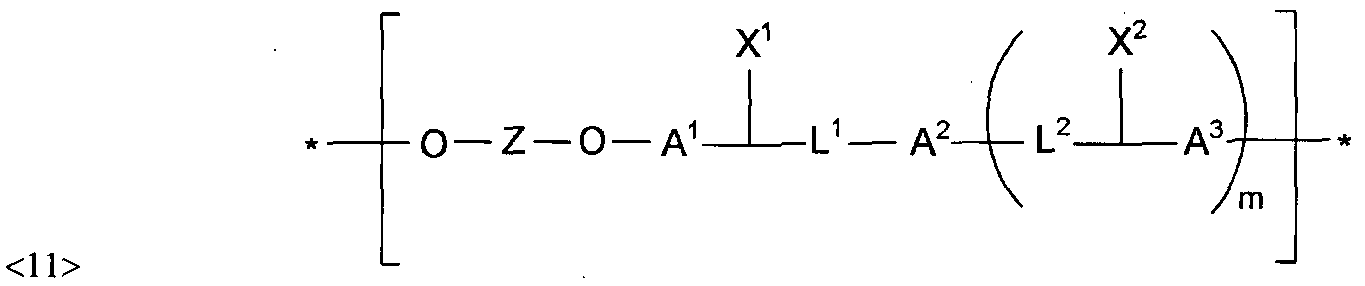
- a resist underlayer film composition comprising a compound and a solvent comprising a moiety represented by the following formula (1).
- a 1 to A 3 are each independently an aliphatic ring group or an aromatic ring group, and each of X 1 and X 2 is independently hydrogen, hydroxy group, thionyl group, thiol group, cyano group, or substituted group. Or an unsubstituted amino group, halogen atom, halogen-containing group or a combination thereof,
- L 1 and L 2 are each independently a single bond or a substituted or unsubstituted C1 to C6 alkylene group
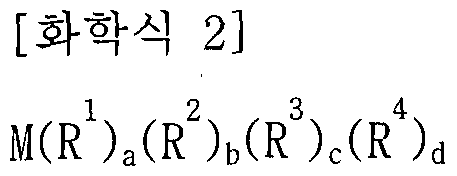
- ⁇ 16> Z is a metal-containing group represented by the following formula (2),
- M is 0 or 1
- ⁇ 21> M is a metal
- R 1 , R, R 3 and R 4 are each independently hydrogen, a hydroxyl group, a substituted or unsubstituted
- A, b, c and d are each independently 0 or 1.
- the metal may be Sc, Ti, V, Cr, Mn, Fe, Co, Ni, Cu, Zn, Zr, Mo, Ag, Cd, Pt, Au, Hf, Rf or Rg.
- a 1 to A 3 may each independently be a substituted or unsubstituted ring group selected from Group 1 below. [Group 1]
- At least one of A 1 to A 3 may be a polycyclic aromatic group.
- a 1 and A 3 are each independently a benzene group, a naphthalene group or a biphenyl group.
- the A ' may be a pyrene group, a perylene group, a benzoperylene group or a coronene group.
- the compound may include a moiety represented by the following Chemical Formula 3.
- a 1 to A 6 are each independently an aliphatic ring group or an aromatic ring group, and each of X 1 to X 4 is independently hydrogen, a hydroxy group, a thionyl group, a thiol group, a cyano substituted or unsubstituted group.
- L and L " are each independently a single bond or a substituted or unsubstituted C1 to C6 alkylene group
- Z is a metal-containing group represented by the formula (2)
- ⁇ 4i> m is 0 or 1
- N is an integer of 1 to 15.
- a 1 to A 6 may be each independently a substituted or unsubstituted ring group selected from Group 1.
- k ⁇ A 3 , A 4, and A 6 are each independently a benzene group, a naphthalene group, or a biphenyl group, and A 2 and A 5 are each independently a pyrene group, a perylene group, It may be a benzoperylene group or coronene group.
- the compound may be represented by the following formula (4).
- the compound may be represented by the following formula (5). [Formula 5] -L 1 ⁇ A 2 ⁇ X 5 In Chemical Formula 5,
- x 1 and x 5 are each independently hydrogen, hydroxy group, thionyl group, thiol group, cyano group, substituted or unsubstituted amino group, halogen atom, halogen-containing group, or a combination thereof.
- the compound may be included in an amount of 0.01 wt% to 50 wt% based on 100 wt% of the solvent.
- the solvent may include at least one selected from propylene glycol monomethyl ether acetate (PGMEA), propylene glycol monomethyl ether (PGME), cyclonucleanone and ethyl lactate.
- PGMEA propylene glycol monomethyl ether acetate
- PGME propylene glycol monomethyl ether
- cyclonucleanone ethyl lactate
- a step of providing a material layer on a substrate applying the above-described composition for a resist underlayer film on the material layer, heat-treating the composition for a resist underlayer film to form a resist underlayer film, on the resist underlayer film Forming a photoresist layer on the substrate; exposing and developing the photoresist layer to form a photoresist pattern; selectively removing the resist underlayer film using the photoresist pattern and exposing a portion of the material layer And etching the exposed portion of the material layer.
- the forming of the resist underlayer film may be performed by a spin-on-coating method.
- the heat treatment of the resist underlayer film composition may be performed at 150 ° C to 500 ° C.
- the method may further include forming a bottom anti-reflection layer (BARC) before forming the resist underlayer.
- BARC bottom anti-reflection layer
- a semiconductor integrated circuit device including a plurality of patterns formed by the above method is provided.
- substituted means a hydrogen atom in a compound having a halogen atom (F, CI, Br or 1), hydroxy group, alkoxy group, nitro group, cyano group, amino group, azi Pottery, amidino group, hydrazino group, hydrazono group, carbonyl group, carbamyl group, thil group, ester group, carboxyl group or salt thereof, sulfonic acid group or salt thereof, phosphoric acid or salt thereof, C1 to C20 alkyl group, C2 to C20 Alkenyl group, C2 to C20 alkynyl group, C6 to C30 aryl group, C7 to C30 arylalkyl group, C1 to C4 alkoxy group, C1 to C20 heteroalkyl group, C3 to C20 heteroarylalkyl group, C3 to C30 cycloalkyl group, C3 to C15 It means substituted with a substituent selected from a halogen atom (F, CI, Br
- hetero means containing 1 to 3 heteroatoms selected from N, 0, S, and P.
- composition for resist underlayer film includes a compound and a solvent including a part represented by the following Chemical Formula 1.
- a 1 to A 3 are each independently an aliphatic or aromatic ring group, and X 1 and X 2 are each independently hydrogen, a hydroxyl group, a thionyl group, a thiol group, a cyano group, a substituted or unsubstituted group.
- L 1 and L 2 are each independently a single bond or a substituted or unsubstituted C1 to C6 alkylene group
- Z is a metal containing group
- M is 0 or 1;
- * indicates a point at which the moiety is linked to the compound.
- the moiety represented by Formula 1 includes at least two aliphatic ring groups or aromatic ring groups, and a plurality of functional groups (X 1 and X 2 ) are located between the aliphatic ring groups or aromatic ring groups. It has three excellent solubility and it is easy to adjust the property according to the substituent. In particular, the solubility may be further improved by the plurality of functional groups (X 1 and X 2 ) to be effectively formed by the spin-on coating method, and the spin-on coating method may be formed on the lower layer having a predetermined pattern. The gap-fill characteristics and planarization characteristics that can fill the gap between the patterns are also excellent.
- the part represented by Chemical Formula 1 may crosslink to a high molecular weight polymer form within a short time even when heat treated at a relatively low temperature, and thus may exhibit characteristics required in a resist underlayer film such as excellent mechanical properties, heat resistance, and etching resistance.
- At least one of k to A 3 representing an aliphatic ring group or an aromatic ring may have at least one hydrogen substituted with a hydroxy group.
- the part represented by Chemical Formula 1 includes a metal containing group.
- the metal-containing group is connected to oxygen on each side, and oxygen connected to one of them is connected to a portion including the aliphatic or aromatic ring group described above.
- M is a metal
- R 1 , R, R and R 4 are each independently hydrogen, a hydroxyl group, a substituted or unsubstituted group.
- A, b, c and d are each independently 0 or 1.
- the metal represented by M in Chemical Formula 2 may satisfy Chemical Formula 2. All metals on the periodic table are included.
- the metal may be a metal having 2 to 6 valence electrons.
- the metal is, for example, Be, Mg, Ca, Cr,
- It may be Sr, Ba or Ra.
- the metal represented by M may be a transition metal.
- the metal may be, for example, Sc, Ti, V, Cr, Mn, Fe, Co, Ni, Cu, Zn, Zr, Mo, Ag, Cd, Pt, Au, Hf, Rf or Rg, but is not limited thereto.
- the metal when a and b are 0 and c and d are 1, the metal may be Ti.
- R 3 and R 4 are each independently hydrogen, a hydroxy group, a substituted or unsubstituted C1 to C10 alkyl group, a substituted or unsubstituted C6 to C10 aryl group, an allyl group, a halogen atom, a substituted or unsubstituted amino group And substituted or unsubstituted C1 to C10 alkoxy groups.
- R 3 and R 4 may be a C1 to C10 alkoxy group substituted with at least one hydrogen valent metal.
- the part represented by Chemical Formula 1 has a structure including a metal, and thus the compound may reduce reactivity with respect to an etch gas. Accordingly, the etch resistance is increased, so that the composition for resist underlayer film can have good etching resistance.
- a 1 to A 3 may be each independently a substituted or unsubstituted ring group selected from Group 1 below.
- each ring is not particularly limited, and each ring may be substituted or unsubstituted.
- the ring listed in Group 1 is a substituted ring, it may be substituted with, for example, a C1 to C20 alkyl group, a halogen atom, or a hydroxy group.
- the substituent is not limited.
- a 1 to A 3 may be, for example, a substituted or unsubstituted aromatic group, for example, a benzene group, a naphthalene group, a biphenyl group, a pyrene group, a perylene group, a benzoperylene group, a coronene group, or a combination thereof. have.
- At least one of A 1 to A J may be a polycyclic aromatic group, for example, a pyrene group, a perylene group, a benzoperylene group, a coronene group, or a combination thereof.
- a 1 and A 3 may be each independently a benzene group, a naphthalene group or a biphenyl group, and A 2 may be a pyrene group, a perylene group, a benzoperylene group, or a coronene group.
- the compound may include a moiety represented by the following Chemical Formula 3.
- a 1 to A 6 are each independently an aliphatic or aromatic ring group
- X 1 to X 4 are each independently hydrogen, a hydroxyl group, a thionyl group, a thiol group, a cyano group, or a substitution Unsubstituted amino group, halogen atom.
- L 1 and L 2 are each independently a single bond or a substituted or unsubstituted C1 to C6 alkylene group
- Z is a metal-containing group represented by the formula (2)
- ⁇ U0> m is 0 or 1
- n is an integer of 1 to 15.
- the moiety represented by Chemical Formula 3 is a structure in which the moiety represented by Chemical Formula 1 is bonded to a monomer including an aliphatic ring group or an aromatic ring group.
- N is the number of repetitions of the moiety represented by Formula 1, and n By adjusting, the metal content of the compound can be controlled.
- a 1 to A 6 may be each independently a substituted or unsubstituted ring group selected from Group 1.
- a 1 , A 3 . A 4 and A 6 are each independently a benzene group, a naphthalene group or a biphenyl group, and each of A 2 and A 5 may independently be a pyrene group, a perylene group, a benzoperylene group or a coronene group.
- At least one of A 1 to A 6 may be substituted with at least one hydrogen hydroxy group.
- the compound may be represented by the following Chemical Formula 4.
- the compound may be represented by the following Formula 5.
- X is hydrogen, hydroxy group, thionyl group, thiol group, cyano group. It is a substituted or unsubstituted amino group, a halogen atom, a halogen containing group, or a combination thereof, and the definition of other subscripts is as above-mentioned.
- the compound may have a weight average molecular weight of about 1.000 to 200,000. By having a weight average molecular weight in the above range, the solubility and coating property of the composition for resist underlayer film can be improved. Within this range, the compound may have a weight average molecular weight of about 5,000 to 10 000.
- the solvent is not particularly limited as long as it has a good solubility or dispersibility in the compound.
- the compound may be included in an amount of about 0.01 wt% to 50 wt% based on 100 wt 3 ⁇ 4 of the solvent. By being included in the above range, the solubility of the composition for resist underlayer film and coating property at the time of film formation can be improved. It may be included in the range of about 0.3 wt% to 20 wt 3 ⁇ 4 within this range.
- the resist underlayer film composition may further include additives such as a surfactant and a crosslinking agent.
- the surfactant may be, for example, alkylbenzenesulfonate salt, alkylpyridinium salt, polyethylene glycol, or quaternary ammonium salt, but is not limited thereto.
- the crosslinking agent is capable of crosslinking the repeating unit of the polymer by heating, and includes an amino resin such as an etherified amino resin; Glycoluril compounds such as compounds represented by the following formula (A); Bisepoxy compound like the compound represented by following formula (B); Melamine or derivatives thereof such as N-methoxymethyl melamine, N ⁇ butoxymethyl melamine or melamine derivatives represented by the following general formula (C); Or combinations thereof.
- an amino resin such as an etherified amino resin
- Glycoluril compounds such as compounds represented by the following formula (A)
- Melamine or derivatives thereof such as N-methoxymethyl melamine, N ⁇ butoxymethyl melamine or melamine derivatives represented by the following general formula (C); Or combinations thereof.
- the surfactant and the crosslinking agent are added to 100% by weight of the composition for resist underlayer film. From about 0.001% to 3% by weight, respectively. By including in the said range, solubility and crosslinkability can be ensured without changing the optical characteristic of the composition for resist underlayer films.
- composition for a resist underlayer film may not be dissolved in a solvent for resist and / or a developer for forming a resist, and may not be mixed with a resist solution to be process chemically stable.
- a method of forming a pattern includes: providing a material layer on a substrate, applying a composition for a resist underlayer film including the polymer and a solvent on the material layer, and heat treating the composition for a resist underlayer film. Forming a resist underlayer film; forming a resist layer on the resist underlayer film; exposing and developing the resist layer; forming a resist pattern; selectively removing the resist underlayer film by using the resist pattern; Exposing a portion of the layer, and etching the exposed portion of the material layer.
- the substrate may be, for example, a silicon wafer, a glass substrate, or a polymer substrate.
- the material layer may be a material to be finally patterned, and may be, for example, a metal layer such as aluminum or copper, a semiconductor layer such as silicon, or an insulating layer such as silicon oxide or silicon nitride.
- the material layer can be formed, for example, by chemical vapor deposition.
- the resist underlayer composition may be prepared in a solution form and applied by spin-on-coat coating.
- the coating thickness of the composition for resist underlayer film is not particularly limited, for example, may be applied to a thickness of about 80A to ⁇ , ⁇ .
- the method may further include forming a bottom anti-reflective layer BARC before forming the resist underlayer film.
- the heat treatment of the composition for resist underlayer film may be performed at, for example, about 150 ° C.
- the polymer may be crosslinked.
- the exposing the resist layer may be performed using, for example, ArF., KrF, or EUV.
- the heat treatment process may be performed at about 100 ° C to 500 ° C after exposure.
- Etching the exposed portion of the material layer may be performed by dry etching using an etching gas, which may be, for example, CHF 3 , CF 4 Cl 2 , BC1 3, and a combination thereof. Can be.
- the etched material layer may be formed in a plurality of patterns, and the plurality of patterns may be varied in a metal pattern, a semiconductor pattern, an insulation pattern, and the like, and may be applied in various patterns in a semiconductor integrated circuit device. Can be.
- ⁇ i6i> A solution was prepared by adding 10 g of the compound obtained in step 3 into a flask and adding 50 ⁇ of tetrahydrofuran. To the solution was slowly added 7.6 g of aqueous sodium borohydride solution and stirred at room temperature for 24 hours. After the reaction was completed, the mixture was neutralized to about pH 7 using a 10% hydrogen chloride solution and extracted with ethyl acetate to obtain a compound represented by Chemical Formula A2. The molecular weight of the compound represented by the following formula (A2) was 1008.97.
- step 3 compound lO.Og represented by Chemical Formula B1 was added to a flask, and tetrahydrofuran 50 was added to prepare a solution. 12.2 g of aqueous sodium borohydride solution was slowly added to the solution, followed by stirring at room temperature for 24 hours. When the reaction was completed, the mixture was neutralized to about pH 7 with 10% hydrogen chloride solution and extracted with ethyl acetate to obtain a compound represented by the following Chemical Formula B2.
- the molecular weight of the compound represented by the following formula (B2) was in the range of about 1,200 to 14,000.
- 1,2-dichloroethane 250ra was added and stirred for 10 minutes at room temperature. Subsequently, 26.3 g of aluminum chloride was slowly added, the temperature was raised to 601: and stirred for 8 hours. After the reaction was completed, methanol was added, and the precipitate formed was filtered to obtain bis (methoxypyrenycarbonyl) benzene. ⁇ 197> Step 2. Demethylation Removal
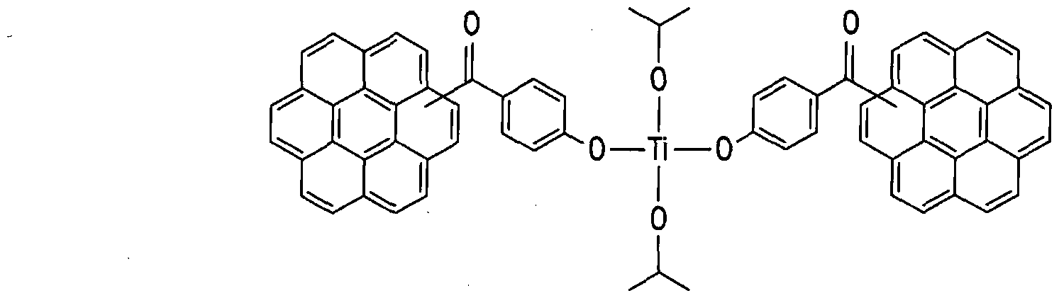
- step 2 25 g of bis (hydroxypyrenylcarbonyl) benzene obtained in step 2 was dissolved in 100 ⁇ £ of tetrahydrofuran, and 6.3 g of titanium isopropoxide was added thereto, followed by reaction for 12 hours at silver. . After the reaction was completed, it was dried to obtain a compound represented by the formula (D1).
- the solution was prepared by adding 330 g. Subsequently, 22.2 g of aluminum chloride was slowly added to the solution at room temperature, and then heated to 60 ° C. and stirred for 8 hours. Upon completion of the reaction, the precipitate formed by adding methanol to the solution was filtered to obtain benzoyl coronene.
- the solution was prepared by adding 25.0 g of the double substituted benzoyl coronene obtained in the first step and 174 g of tetrahydrofuran to the flask. 18.6 g of aqueous sodium borohydride solution was slowly added to the solution, followed by stirring at room temperature for 24 hours. When the reaction was completed, neutralized with a 10% hydrogen chloride solution to pH 7 and extracted with ethyl acetate to obtain a monomer represented by the formula (E).
- a solution was prepared by adding 50.0 g (0.166 mol) of coronene, 46.8 g (0.333 mol) of benzoyl chloride and 330 g of 1,2-dichloroethane to a ⁇ 2i8> flask. Then into the solution 44.4 g (0.333 mol) of aluminum chloride was slowly added at room temperature, and then heated to 60 ° C. and stirred for 8 hours. Upon completion of the reaction, precipitated ol formed by adding methanol to the solution to obtain a double substituted benzoyl coronene.
- a solution was prepared by adding 25.0 g (0.0492 mol) of double substituted benzoyl coronene obtained in the first step and 174 g of tetrahydrofuran to the flask. 18.6 g (0.492 mol) ol of aqueous sodium borohydride solution was slowly added to the solution, followed by stirring at room temperature for 24 hours. Upon completion of the reaction, the mixture was neutralized with a 10% hydrogen chloride solution to pH 7 and extracted with ethyl acetate to obtain a monomer represented by the following Formula F.
- 1st fry In a Friedel-Craft Acvlation reaction flask, 13.9 g (0.0989 mol) of benzoyl chloride, 10.0 g (0.0495 mol) of pyrene and 87 g of 1,2-dichloroethane were added. 13.2 g (0.0989 mol) of aluminum chloride was slowly added to the solution at room temperature, and then heated to 60 ° C. and stirred for 8 hours. When reaction was completed, the precipitate formed after adding methane was filtered to obtain dibenzoylpyrene.
- the solution was placed in a separatory funnel, n-heptane was added to remove the monomer and the low molecular weight body, thereby obtaining a polymer represented by the following formula (H).
- the weight average molecular weight of the polymer was 12,000, and the degree of dispersion was 2.04.
- a resist underlayer film composition was prepared in the same manner as in Example 1 except that the compound represented by Chemical Formula B2 obtained in Synthesis Example 2 was used instead of the compound obtained in Synthesis Example 1.
- Example 3 A resist underlayer film composition was prepared in the same manner as in Example 1 except that the compound represented by Chemical Formula C2 obtained in Synthesis Example 3 was used instead of the compound obtained in Synthesis Example 1.
- a composition for a resist underlayer film was prepared in the same manner as in Example 1 except that the compound represented by Chemical Formula D2 obtained in Synthesis Example 4 was used instead of the compound obtained in Synthesis Example 1.
- a composition for a resist underlayer film was prepared in the same manner as in Example 1 except that the compound obtained in Comparative Synthesis Example 1 was used instead of the compound obtained in Synthesis Example 1.
- a composition for resist underlayer film was prepared in the same manner as in Example 1 except that the compound obtained in Comparative Synthesis Example 2 was used instead of the compound obtained in Synthesis Example 1.
- composition for resist underlayer film was prepared in the same manner as in Example 1 except that the compound obtained in Comparative Synthesis Example 3 was used instead of the compound obtained in Synthesis Example 1.
- a composition for a resist underlayer film was prepared in the same manner as in Example 1 except that the compound obtained in Comparative Synthesis Example 4 was used instead of the compound obtained in Synthesis Example 1.
- composition for a resist underlayer film according to Examples 1 to 4 and Comparative Examples 1 to 4 was spin coated on a silicon wafer and baked at 200 ° C. for 60 seconds to form a Resin E underlayer film having a thickness of 4000 A.
- the refractive index (n) and extinction coefficient (k) of each hard mask layer were measured using an Ellipsometer (J. A. Woollam).
- Example 1 a resist lower layer film composition according to to 4 ArF
- composition for resist underlayer film according to Examples 1 to 4 and Comparative Examples 1 to 3 was spin coated on a silicon wafer and heat-treated at 240 ° C. for 120 seconds to measure the thickness of the coated thin film. Observed. Subsequently, the film thickness was measured after immersion in KrF thinner for 1 minute and the surface of the thin film was observed.
- the thin film thickness was measured under the same conditions as above except that the heat treatment temperature was changed from 24 CTC to 400 ° C., and the surface of the thin film was observed.
- the thickness reduction rate was calculated by the following equation 1 from the thin film thickness before and after immersion.
- Example 1 a thin film formed from the resist lower layer film composition according to to 4 is 240 No rust was observed on the surface of the thin film at both ° C and 400 ° C, indicating good chemical resistance.
- the thin film formed from the resist underlayer film composition according to Examples 1 to 4 has a small thickness difference before and after immersion as compared with the thin film formed from the resist underlayer film composition according to Comparative Examples 1 to 3.
- composition for the resist underlayer film according to Examples 1 to 4 has a relatively high degree of crosslinking compared to the composition for the resist underlayer film according to Comparative Examples 1 to 3, and accordingly to Examples 1 to 4 It can be seen that the composition for resist underlayer film has excellent chemical resistance.
- composition for a resist underlayer film according to Examples 1 to 4 and Comparative Examples 1 to 4 was spin coated on a silicon wafer and thermally treated at 240 ° C. for 120 seconds to measure the thickness of the coated thin film.
- the bulk etch rate (BER) was calculated by the following equation (2).
- the thin film formed from the composition for resist underlayer film according to Examples 1 to 4 has a layered etching resistance against the etching gas in comparison with the thin film formed from the hard mask composition according to Comparative Examples 1 to 4. Confirm that it indicates low etching It can be cut.
Landscapes
- Physics & Mathematics (AREA)
- General Physics & Mathematics (AREA)
- Engineering & Computer Science (AREA)
- Architecture (AREA)
- Structural Engineering (AREA)
- Spectroscopy & Molecular Physics (AREA)
- Chemical & Material Sciences (AREA)
- Organic Chemistry (AREA)
- Materials For Photolithography (AREA)
- Organic Low-Molecular-Weight Compounds And Preparation Thereof (AREA)
- Exposure And Positioning Against Photoresist Photosensitive Materials (AREA)
- Exposure Of Semiconductors, Excluding Electron Or Ion Beam Exposure (AREA)
Abstract
Description




Claims






Priority Applications (3)
| Application Number | Priority Date | Filing Date | Title |
|---|---|---|---|
| JP2016515251A JP6304726B2 (ja) | 2013-05-21 | 2013-11-05 | レジスト下層膜用組成物、これを用いたパターン形成方法および前記パターンを含む半導体集積回路デバイス |
| US14/782,539 US9606438B2 (en) | 2013-05-21 | 2013-11-05 | Resist underlayer composition, method of forming patterns, and semiconductor integrated circuit device including the pattern |
| CN201380075787.1A CN105229532B (zh) | 2013-05-21 | 2013-11-05 | 抗蚀剂底层组合物、图案形成方法及含有图案的半导体集成电路装置 |
Applications Claiming Priority (2)
| Application Number | Priority Date | Filing Date | Title |
|---|---|---|---|
| KR1020130057256A KR101674989B1 (ko) | 2013-05-21 | 2013-05-21 | 레지스트 하층막용 조성물, 이를 사용한 패턴 형성 방법 및 상기 패턴을 포함하는 반도체 집적회로 디바이스 |
| KR10-2013-0057256 | 2013-05-21 |
Publications (1)
| Publication Number | Publication Date |
|---|---|
| WO2014189185A1 true WO2014189185A1 (ko) | 2014-11-27 |
Family
ID=51933719
Family Applications (1)
| Application Number | Title | Priority Date | Filing Date |
|---|---|---|---|
| PCT/KR2013/009957 Ceased WO2014189185A1 (ko) | 2013-05-21 | 2013-11-05 | 레지스트 하층막용 조성물, 이를 사용한 패턴 형성 방법 및 상기 패턴을 포함하는 반도체 집적회로 디바이스 |
Country Status (6)
| Country | Link |
|---|---|
| US (1) | US9606438B2 (ko) |
| JP (1) | JP6304726B2 (ko) |
| KR (1) | KR101674989B1 (ko) |
| CN (1) | CN105229532B (ko) |
| TW (1) | TWI529493B (ko) |
| WO (1) | WO2014189185A1 (ko) |
Cited By (1)
| Publication number | Priority date | Publication date | Assignee | Title |
|---|---|---|---|---|
| WO2017099192A1 (ja) * | 2015-12-09 | 2017-06-15 | 東京応化工業株式会社 | 有機金属化合物 |
Families Citing this family (5)
| Publication number | Priority date | Publication date | Assignee | Title |
|---|---|---|---|---|
| TWI592760B (zh) * | 2014-12-30 | 2017-07-21 | 羅門哈斯電子材料韓國有限公司 | 與經外塗佈之光致抗蝕劑一起使用之塗層組合物 |
| KR102047538B1 (ko) * | 2017-02-03 | 2019-11-21 | 삼성에스디아이 주식회사 | 레지스트 하층막용 조성물 및 이를 이용한 패턴형성방법 |
| KR102264695B1 (ko) * | 2018-05-25 | 2021-06-11 | 삼성에스디아이 주식회사 | 레지스트 하층막용 조성물 및 이를 이용한 패턴형성방법 |
| KR102264693B1 (ko) | 2018-06-11 | 2021-06-11 | 삼성에스디아이 주식회사 | 레지스트 하층막용 조성물 및 이를 이용한 패턴형성방법 |
| KR102758734B1 (ko) * | 2021-07-30 | 2025-01-21 | 삼성에스디아이 주식회사 | 레지스트 하층막용 조성물 및 이를 이용한 패턴형성방법 |
Citations (6)
| Publication number | Priority date | Publication date | Assignee | Title |
|---|---|---|---|---|
| US20060222999A1 (en) * | 2003-08-21 | 2006-10-05 | Asahi Kasei Chemicals Corporation | Photosensitive composition and cured products thereof |
| US20110027717A1 (en) * | 2008-04-04 | 2011-02-03 | Kiyoharu Tsutsumi | Photoresist composition |
| US20110155944A1 (en) * | 2009-12-31 | 2011-06-30 | Cho Sung-Wook | Aromatic ring-containing compound for a resist underlayer and resist underlayer composition |
| KR101067828B1 (ko) * | 2003-06-06 | 2011-09-27 | 후지필름 일렉트로닉 머티리얼스 유.에스.에이., 아이엔씨. | 신규한 감광성 수지 조성물들 |
| KR20120073101A (ko) * | 2010-12-24 | 2012-07-04 | 후지필름 가부시키가이샤 | 감활성광선성 또는 감방사선성 수지 조성물과 이 조성물을 사용한 감활성광선성 또는 감방사선성 막 및 패턴 형성 방법 |
| KR101257694B1 (ko) * | 2009-06-29 | 2013-04-24 | 제일모직주식회사 | 레지스트 하층막용 방향족 고리 함유 중합체, 이 중합체의 제조 방법, 이 중합체를 포함하는 레지스트 하층막 조성물, 및 이를 이용하는 소자의 패턴 형성 방법 |
Family Cites Families (20)
| Publication number | Priority date | Publication date | Assignee | Title |
|---|---|---|---|---|
| US6287975B1 (en) | 1998-01-20 | 2001-09-11 | Tegal Corporation | Method for using a hard mask for critical dimension growth containment |
| JP4057762B2 (ja) | 2000-04-25 | 2008-03-05 | 株式会社ルネサステクノロジ | 半導体装置の製造方法 |
| JP4626096B2 (ja) | 2001-06-15 | 2011-02-02 | Jsr株式会社 | カラーフィルタ用感放射線性組成物、カラーフィルタおよびカラー液晶表示素子 |
| JP2005173552A (ja) | 2003-11-20 | 2005-06-30 | Tokyo Ohka Kogyo Co Ltd | リソグラフィー用下層膜形成材料およびこれを用いた配線形成方法 |
| JP4793583B2 (ja) | 2004-10-14 | 2011-10-12 | 日産化学工業株式会社 | 金属酸化物を含むリソグラフィー用下層膜形成組成物 |
| JP4421566B2 (ja) * | 2005-12-26 | 2010-02-24 | チェイル インダストリーズ インコーポレイテッド | フォトレジスト下層膜用ハードマスク組成物及びこれを利用した半導体集積回路デバイスの製造方法 |
| KR100864375B1 (ko) | 2006-01-03 | 2008-10-21 | 주식회사 에스앤에스텍 | 블랭크 마스크 및 이를 이용한 포토마스크의 제조방법 |
| US8168372B2 (en) * | 2006-09-25 | 2012-05-01 | Brewer Science Inc. | Method of creating photolithographic structures with developer-trimmed hard mask |
| KR100816735B1 (ko) | 2006-12-20 | 2008-03-25 | 제일모직주식회사 | 반사방지 하드마스크 조성물, 이를 이용한 패턴화된 재료형상의 제조방법 및 반도체 집적회로 디바이스 |
| KR100896451B1 (ko) | 2006-12-30 | 2009-05-14 | 제일모직주식회사 | 카본 함량이 개선된 고 내에칭성 반사방지 하드마스크조성물, 이를 이용한 패턴화된 재료 형상의 제조방법 |
| KR20080081584A (ko) | 2007-03-06 | 2008-09-10 | 주식회사 에스앤에스텍 | 블랭크 마스크 및 이를 이용한 포토마스크의 제조방법 |
| KR100888613B1 (ko) | 2007-08-10 | 2009-03-12 | 제일모직주식회사 | 포토레지스트 하층막용 하드마스크 조성물 및 이를 이용한반도체 집적회로 디바이스의 제조방법 |
| RU2489450C9 (ru) * | 2007-10-17 | 2014-01-27 | Басф Се | Фотолатентные катализаторы на основе металлорганических соединений |
| KR101156488B1 (ko) | 2008-12-22 | 2012-06-18 | 제일모직주식회사 | 하드마스크 층 형성용 조성물 및 이를 사용한 패턴화된 재료 형상의 제조방법 |
| JP5627195B2 (ja) * | 2009-04-27 | 2014-11-19 | 東海旅客鉄道株式会社 | 感光性組成物、感光性金属錯体、塗布液、及び金属酸化物薄膜パターンの製造方法 |
| JP5502092B2 (ja) | 2009-09-15 | 2014-05-28 | シャープ株式会社 | 蒸着方法および蒸着装置 |
| KR101414278B1 (ko) * | 2009-11-13 | 2014-07-02 | 제일모직 주식회사 | 레지스트 하층막용 고분자, 이를 포함하는 레지스트 하층막 조성물 및 소자의 패턴 형성 방법 |
| JP5453361B2 (ja) * | 2011-08-17 | 2014-03-26 | 信越化学工業株式会社 | ケイ素含有レジスト下層膜形成用組成物、及びパターン形成方法 |
| US9315636B2 (en) * | 2012-12-07 | 2016-04-19 | Az Electronic Materials (Luxembourg) S.A.R.L. | Stable metal compounds, their compositions and methods |
| JP6311702B2 (ja) * | 2013-03-25 | 2018-04-18 | Jsr株式会社 | 多層レジストプロセス用無機膜形成組成物及びパターン形成方法 |
-
2013
- 2013-05-21 KR KR1020130057256A patent/KR101674989B1/ko active Active
- 2013-11-05 WO PCT/KR2013/009957 patent/WO2014189185A1/ko not_active Ceased
- 2013-11-05 JP JP2016515251A patent/JP6304726B2/ja active Active
- 2013-11-05 CN CN201380075787.1A patent/CN105229532B/zh active Active
- 2013-11-05 US US14/782,539 patent/US9606438B2/en active Active
- 2013-11-14 TW TW102141368A patent/TWI529493B/zh active
Patent Citations (6)
| Publication number | Priority date | Publication date | Assignee | Title |
|---|---|---|---|---|
| KR101067828B1 (ko) * | 2003-06-06 | 2011-09-27 | 후지필름 일렉트로닉 머티리얼스 유.에스.에이., 아이엔씨. | 신규한 감광성 수지 조성물들 |
| US20060222999A1 (en) * | 2003-08-21 | 2006-10-05 | Asahi Kasei Chemicals Corporation | Photosensitive composition and cured products thereof |
| US20110027717A1 (en) * | 2008-04-04 | 2011-02-03 | Kiyoharu Tsutsumi | Photoresist composition |
| KR101257694B1 (ko) * | 2009-06-29 | 2013-04-24 | 제일모직주식회사 | 레지스트 하층막용 방향족 고리 함유 중합체, 이 중합체의 제조 방법, 이 중합체를 포함하는 레지스트 하층막 조성물, 및 이를 이용하는 소자의 패턴 형성 방법 |
| US20110155944A1 (en) * | 2009-12-31 | 2011-06-30 | Cho Sung-Wook | Aromatic ring-containing compound for a resist underlayer and resist underlayer composition |
| KR20120073101A (ko) * | 2010-12-24 | 2012-07-04 | 후지필름 가부시키가이샤 | 감활성광선성 또는 감방사선성 수지 조성물과 이 조성물을 사용한 감활성광선성 또는 감방사선성 막 및 패턴 형성 방법 |
Cited By (2)
| Publication number | Priority date | Publication date | Assignee | Title |
|---|---|---|---|---|
| WO2017099192A1 (ja) * | 2015-12-09 | 2017-06-15 | 東京応化工業株式会社 | 有機金属化合物 |
| JPWO2017099192A1 (ja) * | 2015-12-09 | 2018-09-27 | 東京応化工業株式会社 | 有機金属化合物 |
Also Published As
| Publication number | Publication date |
|---|---|
| KR20140136767A (ko) | 2014-12-01 |
| US9606438B2 (en) | 2017-03-28 |
| CN105229532B (zh) | 2019-12-10 |
| TW201445257A (zh) | 2014-12-01 |
| CN105229532A (zh) | 2016-01-06 |
| KR101674989B1 (ko) | 2016-11-22 |
| JP6304726B2 (ja) | 2018-04-04 |
| US20160041470A1 (en) | 2016-02-11 |
| TWI529493B (zh) | 2016-04-11 |
| JP2016521863A (ja) | 2016-07-25 |
Similar Documents
| Publication | Publication Date | Title |
|---|---|---|
| TWI642698B (zh) | 作為硬光罩及填充材料之穩定金屬化合物、其組合物及其使用方法 | |
| JP6084986B2 (ja) | ハードマスク組成物用モノマー、前記モノマーを含むハードマスク組成物および前記ハードマスク組成物を用いたパターン形成方法 | |
| CN103959170B (zh) | 用于硬掩模组合物的单体、包括单体的硬掩模组合物以及使用硬掩模组合物的图案形成方法 | |
| KR101556275B1 (ko) | 모노머, 상기 모노머를 포함하는 하드마스크 조성물 및 상기 하드마스크 조성물을 사용하는 패턴형성방법 | |
| TWI525062B (zh) | 抗蝕劑底層組成物、圖案形成方法及含有該圖案的半導體積體電路裝置 | |
| KR101666483B1 (ko) | 레지스트 하층막용 조성물, 이를 사용한 패턴 형성 방법 및 상기 패턴을 포함하는 반도체 집적회로 디바이스 | |
| TW201500857A (zh) | 用於硬罩幕組合物的單體、包括該單體的硬罩幕組合物及使用該硬罩幕組合物的形成圖案的方法 | |
| WO2014189185A1 (ko) | 레지스트 하층막용 조성물, 이를 사용한 패턴 형성 방법 및 상기 패턴을 포함하는 반도체 집적회로 디바이스 | |
| KR101413071B1 (ko) | 하드마스크 조성물용 모노머, 상기 모노머를 포함하는 하드마스크 조성물 및 상기 하드마스크 조성물을 사용하는 패턴형성방법 | |
| WO2017126780A1 (ko) | 유기막 조성물, 및 패턴형성방법 | |
| KR20160008927A (ko) | 하드마스크 조성물 및 상기 하드마스크 조성물을 사용하는 패턴형성방법 | |
| KR101684977B1 (ko) | 하드마스크 조성물, 이를 사용한 패턴 형성 방법 및 상기 패턴을 포함하는 반도체 집적회로 디바이스 | |
| WO2014104544A1 (ko) | 하드마스크 조성물용 모노머, 상기 모노머를 포함하는 하드마스크 조성물 및 상기 하드마스크 조성물을 사용하는 패턴형성방법 | |
| KR101590809B1 (ko) | 하드마스크 조성물용 모노머, 상기 모노머를 포함하는 하드마스크 조성물 및 상기 하드마스크 조성물을 사용하는 패턴형성방법 | |
| KR101705756B1 (ko) | 하드마스크 조성물용 모노머, 상기 모노머를 포함하는 하드마스크 조성물 및 상기 하드마스크 조성물을 사용하는 패턴형성방법 | |
| KR101757809B1 (ko) | 모노머, 상기 모노머를 포함하는 하드마스크 조성물 및 상기 하드마스크 조성물을 사용하는 패턴형성방법 | |
| KR101693612B1 (ko) | 하드마스크 조성물용 모노머, 상기 모노머를 포함하는 하드마스크 조성물 및 상기 하드마스크 조성물을 사용하는 패턴형성방법 | |
| KR102815439B1 (ko) | 하드마스크 조성물, 하드마스크 층 및 패턴 형성 방법 | |
| KR101590810B1 (ko) | 모노머, 상기 모노머를 포함하는 하드마스크 조성물 및 상기 하드마스크 조성물을 사용하는 패턴형성방법 | |
| WO2018088658A1 (ko) | 중합체, 유기막 조성물 및 패턴형성방법 |
Legal Events
| Date | Code | Title | Description |
|---|---|---|---|
| WWE | Wipo information: entry into national phase |
Ref document number: 201380075787.1 Country of ref document: CN |
|
| 121 | Ep: the epo has been informed by wipo that ep was designated in this application |
Ref document number: 13885209 Country of ref document: EP Kind code of ref document: A1 |
|
| WWE | Wipo information: entry into national phase |
Ref document number: 14782539 Country of ref document: US |
|
| ENP | Entry into the national phase |
Ref document number: 2016515251 Country of ref document: JP Kind code of ref document: A |
|
| NENP | Non-entry into the national phase |
Ref country code: DE |
|
| 122 | Ep: pct application non-entry in european phase |
Ref document number: 13885209 Country of ref document: EP Kind code of ref document: A1 |