WO2014189028A1 - 導電材料及び接続構造体 - Google Patents
導電材料及び接続構造体 Download PDFInfo
- Publication number
- WO2014189028A1 WO2014189028A1 PCT/JP2014/063290 JP2014063290W WO2014189028A1 WO 2014189028 A1 WO2014189028 A1 WO 2014189028A1 JP 2014063290 W JP2014063290 W JP 2014063290W WO 2014189028 A1 WO2014189028 A1 WO 2014189028A1
- Authority
- WO
- WIPO (PCT)
- Prior art keywords
- conductive
- conductive material
- organic acid
- particles
- layer
- Prior art date
- Legal status (The legal status is an assumption and is not a legal conclusion. Google has not performed a legal analysis and makes no representation as to the accuracy of the status listed.)
- Ceased
Links
Images


Classifications
-
- H—ELECTRICITY
- H01—ELECTRIC ELEMENTS
- H01B—CABLES; CONDUCTORS; INSULATORS; SELECTION OF MATERIALS FOR THEIR CONDUCTIVE, INSULATING OR DIELECTRIC PROPERTIES
- H01B1/00—Conductors or conductive bodies characterised by the conductive materials; Selection of materials as conductors
- H01B1/20—Conductive material dispersed in non-conductive organic material
- H01B1/22—Conductive material dispersed in non-conductive organic material the conductive material comprising metals or alloys
-
- B—PERFORMING OPERATIONS; TRANSPORTING
- B22—CASTING; POWDER METALLURGY
- B22F—WORKING METALLIC POWDER; MANUFACTURE OF ARTICLES FROM METALLIC POWDER; MAKING METALLIC POWDER; APPARATUS OR DEVICES SPECIALLY ADAPTED FOR METALLIC POWDER
- B22F1/00—Metallic powder; Treatment of metallic powder, e.g. to facilitate working or to improve properties
- B22F1/18—Non-metallic particles coated with metal
-
- C—CHEMISTRY; METALLURGY
- C08—ORGANIC MACROMOLECULAR COMPOUNDS; THEIR PREPARATION OR CHEMICAL WORKING-UP; COMPOSITIONS BASED THEREON
- C08J—WORKING-UP; GENERAL PROCESSES OF COMPOUNDING; AFTER-TREATMENT NOT COVERED BY SUBCLASSES C08B, C08C, C08F, C08G or C08H
- C08J3/00—Processes of treating or compounding macromolecular substances
- C08J3/12—Powdering or granulating
- C08J3/128—Polymer particles coated by inorganic and non-macromolecular organic compounds
-
- C—CHEMISTRY; METALLURGY
- C08—ORGANIC MACROMOLECULAR COMPOUNDS; THEIR PREPARATION OR CHEMICAL WORKING-UP; COMPOSITIONS BASED THEREON
- C08L—COMPOSITIONS OF MACROMOLECULAR COMPOUNDS
- C08L101/00—Compositions of unspecified macromolecular compounds
- C08L101/02—Compositions of unspecified macromolecular compounds characterised by the presence of specified groups, e.g. terminal or pendant functional groups
-
- C—CHEMISTRY; METALLURGY
- C08—ORGANIC MACROMOLECULAR COMPOUNDS; THEIR PREPARATION OR CHEMICAL WORKING-UP; COMPOSITIONS BASED THEREON
- C08L—COMPOSITIONS OF MACROMOLECULAR COMPOUNDS
- C08L63/00—Compositions of epoxy resins; Compositions of derivatives of epoxy resins
-
- H—ELECTRICITY
- H05—ELECTRIC TECHNIQUES NOT OTHERWISE PROVIDED FOR
- H05K—PRINTED CIRCUITS; CASINGS OR CONSTRUCTIONAL DETAILS OF ELECTRIC APPARATUS; MANUFACTURE OF ASSEMBLAGES OF ELECTRICAL COMPONENTS
- H05K1/00—Printed circuits
- H05K1/02—Details
- H05K1/09—Use of materials for the conductive, e.g. metallic pattern
-
- H—ELECTRICITY
- H05—ELECTRIC TECHNIQUES NOT OTHERWISE PROVIDED FOR
- H05K—PRINTED CIRCUITS; CASINGS OR CONSTRUCTIONAL DETAILS OF ELECTRIC APPARATUS; MANUFACTURE OF ASSEMBLAGES OF ELECTRICAL COMPONENTS
- H05K3/00—Apparatus or processes for manufacturing printed circuits
- H05K3/30—Assembling printed circuits with electric components, e.g. with resistors
- H05K3/32—Assembling printed circuits with electric components, e.g. with resistors electrically connecting electric components or wires to printed circuits
- H05K3/321—Assembling printed circuits with electric components, e.g. with resistors electrically connecting electric components or wires to printed circuits by conductive adhesives
- H05K3/323—Assembling printed circuits with electric components, e.g. with resistors electrically connecting electric components or wires to printed circuits by conductive adhesives by applying an anisotropic conductive adhesive layer over an array of pads
-
- H—ELECTRICITY
- H05—ELECTRIC TECHNIQUES NOT OTHERWISE PROVIDED FOR
- H05K—PRINTED CIRCUITS; CASINGS OR CONSTRUCTIONAL DETAILS OF ELECTRIC APPARATUS; MANUFACTURE OF ASSEMBLAGES OF ELECTRICAL COMPONENTS
- H05K3/00—Apparatus or processes for manufacturing printed circuits
- H05K3/30—Assembling printed circuits with electric components, e.g. with resistors
- H05K3/32—Assembling printed circuits with electric components, e.g. with resistors electrically connecting electric components or wires to printed circuits
- H05K3/34—Assembling printed circuits with electric components, e.g. with resistors electrically connecting electric components or wires to printed circuits by soldering
- H05K3/3465—Application of solder
-
- H—ELECTRICITY
- H10—SEMICONDUCTOR DEVICES; ELECTRIC SOLID-STATE DEVICES NOT OTHERWISE PROVIDED FOR
- H10W—GENERIC PACKAGES, INTERCONNECTIONS, CONNECTORS OR OTHER CONSTRUCTIONAL DETAILS OF DEVICES COVERED BY CLASS H10
- H10W99/00—Subject matter not provided for in other groups of this subclass
-
- B—PERFORMING OPERATIONS; TRANSPORTING
- B22—CASTING; POWDER METALLURGY
- B22F—WORKING METALLIC POWDER; MANUFACTURE OF ARTICLES FROM METALLIC POWDER; MAKING METALLIC POWDER; APPARATUS OR DEVICES SPECIALLY ADAPTED FOR METALLIC POWDER
- B22F1/00—Metallic powder; Treatment of metallic powder, e.g. to facilitate working or to improve properties
- B22F1/10—Metallic powder containing lubricating or binding agents; Metallic powder containing organic material
- B22F1/102—Metallic powder coated with organic material
-
- B—PERFORMING OPERATIONS; TRANSPORTING
- B22—CASTING; POWDER METALLURGY
- B22F—WORKING METALLIC POWDER; MANUFACTURE OF ARTICLES FROM METALLIC POWDER; MAKING METALLIC POWDER; APPARATUS OR DEVICES SPECIALLY ADAPTED FOR METALLIC POWDER
- B22F1/00—Metallic powder; Treatment of metallic powder, e.g. to facilitate working or to improve properties
- B22F1/16—Metallic particles coated with a non-metal
-
- H—ELECTRICITY
- H05—ELECTRIC TECHNIQUES NOT OTHERWISE PROVIDED FOR
- H05K—PRINTED CIRCUITS; CASINGS OR CONSTRUCTIONAL DETAILS OF ELECTRIC APPARATUS; MANUFACTURE OF ASSEMBLAGES OF ELECTRICAL COMPONENTS
- H05K2201/00—Indexing scheme relating to printed circuits covered by H05K1/00
- H05K2201/02—Fillers; Particles; Fibers; Reinforcement materials
- H05K2201/0203—Fillers and particles
- H05K2201/0206—Materials
- H05K2201/0221—Insulating particles having an electrically conductive coating
-
- H—ELECTRICITY
- H05—ELECTRIC TECHNIQUES NOT OTHERWISE PROVIDED FOR
- H05K—PRINTED CIRCUITS; CASINGS OR CONSTRUCTIONAL DETAILS OF ELECTRIC APPARATUS; MANUFACTURE OF ASSEMBLAGES OF ELECTRICAL COMPONENTS
- H05K3/00—Apparatus or processes for manufacturing printed circuits
- H05K3/30—Assembling printed circuits with electric components, e.g. with resistors
- H05K3/32—Assembling printed circuits with electric components, e.g. with resistors electrically connecting electric components or wires to printed circuits
- H05K3/34—Assembling printed circuits with electric components, e.g. with resistors electrically connecting electric components or wires to printed circuits by soldering
- H05K3/341—Surface mounted components
- H05K3/3431—Leadless components
- H05K3/3436—Leadless components having an array of bottom contacts, e.g. pad grid array or ball grid array components
-
- H—ELECTRICITY
- H05—ELECTRIC TECHNIQUES NOT OTHERWISE PROVIDED FOR
- H05K—PRINTED CIRCUITS; CASINGS OR CONSTRUCTIONAL DETAILS OF ELECTRIC APPARATUS; MANUFACTURE OF ASSEMBLAGES OF ELECTRICAL COMPONENTS
- H05K3/00—Apparatus or processes for manufacturing printed circuits
- H05K3/36—Assembling printed circuits with other printed circuits
- H05K3/361—Assembling flexible printed circuits with other printed circuits
- H05K3/363—Assembling flexible printed circuits with other printed circuits by soldering
-
- H—ELECTRICITY
- H10—SEMICONDUCTOR DEVICES; ELECTRIC SOLID-STATE DEVICES NOT OTHERWISE PROVIDED FOR
- H10W—GENERIC PACKAGES, INTERCONNECTIONS, CONNECTORS OR OTHER CONSTRUCTIONAL DETAILS OF DEVICES COVERED BY CLASS H10
- H10W72/00—Interconnections or connectors in packages
- H10W72/30—Die-attach connectors
Definitions
- the present invention relates to a conductive material including conductive particles, and can be used to electrically connect electrodes of various connection target members such as a flexible printed circuit board, a glass substrate, a glass epoxy substrate, and a semiconductor chip.
- the present invention relates to a conductive material.
- the present invention also relates to a connection structure using the conductive material.
- Pasty or film anisotropic conductive materials are widely known.
- anisotropic conductive material a plurality of conductive particles are dispersed in a binder resin.
- the anisotropic conductive material may be connected between a flexible printed circuit board and a glass substrate (FOG (Film on Glass)), or connected between a semiconductor chip and a flexible printed circuit board (COF ( (Chip on Film)), connection between a semiconductor chip and a glass substrate (COG (Chip on Glass)), connection between a flexible printed circuit board and a glass epoxy substrate (FOB (Film on Board)), and the like.
- FOG Glass
- COF Chip on Film
- Patent Document 1 discloses a conductive adhesive containing an epoxy adhesive having a flux action and SnBi solder powder.
- Patent Document 1 describes that in 100% by weight of the conductive adhesive, the content of solder powder is preferably in the range of 10 to 90% by weight, but preferably 40 to 80% by weight.
- curing agent, and an organic acid is mentioned as an epoxy adhesive which has a flux effect
- Patent Document 1 describes that a small amount of succinic acid, malonic acid, glutaric acid, adipic acid, suberic acid, azelaic acid, sebacic acid, and the like can be added as auxiliary activators.
- 2,5-diethyladipic acid, succinic acid, glutaric acid, and malonic acid are used as the organic acid and the auxiliary activator.
- Patent Document 2 discloses a solder paste containing flux and solder particles.
- the flux includes a silicone resin and an organic acid or an organic acid salt.
- Patent Document 2 describes that regarding the quantity ratio between the flux and the solder particles, it is appropriate to set the flux to 5 to 60 parts by weight with respect to 40 to 95 parts by weight of the solder particles.
- malonic acid, succinic acid, glutaric acid, adipic acid, azelaic acid, sebacic acid, hydroxyacetic acid, and monoethanolamine succinate are used as the organic acid or organic acid salt.
- Patent Document 3 discloses a soldering flux containing an activator obtained by a dibasic acid having a molecular weight of 250 or less and a monobasic acid having a molecular weight of 150 or more and 300 or less. ing.
- Patent Document 4 listed below discloses a solder paste containing an alcohol having at least two OH groups as a flux base agent, an organic acid as a flux activator, and a metal powder.
- JP 2006-199937 A JP 05-92296 A JP-A-9-253484 JP 2000-61689 A
- An object of the present invention is to provide a conductive material having a high reaction rate and a high flux effect, and to provide a connection structure using the conductive material.
- a limited object of the present invention is to provide a conductive material capable of reducing the connection resistance when the electrodes are electrically connected because the flux effect is high, and a connection structure using the conductive material Is to provide a body.
- conductive particles having at least an outer surface of solder, an anion curable compound, an anion curing agent, and an organic acid having a carboxyl group and a functional group esterified with a carboxyl group.
- a conductive material is provided.
- the organic acid which has the functional group by which the said carboxyl group and the carboxyl group were esterified esterifies a part of carboxyl group in the organic acid which has multiple carboxyl groups. It is obtained with.
- the organic acid having a carboxyl group and a functional group in which the carboxyl group is esterified includes an organic acid having a plurality of the carboxyl groups and an alcohol, a part of the carboxyl group. Can be obtained by esterification.
- the conductive material further includes an esterified product obtained by esterifying all of the carboxyl groups in the organic acid having a plurality of carboxyl groups.
- the conductive material further includes an organic acid having a plurality of carboxyl groups and not having a functional group in which the carboxyl groups are esterified.
- the conductive material has an esterified product obtained by esterifying all of the carboxyl groups in the organic acid having a plurality of carboxyl groups, a plurality of carboxyl groups, and And an organic acid having no functional group in which the carboxyl group is esterified.
- the carboxyl group and the organic acid having a functional group in which the carboxyl group is esterified, and all of the carboxyl groups in the organic acid having a plurality of carboxyl groups are esterified.
- Total number of carboxyl groups and functional groups esterified with carboxyl groups in the total of the resulting esterified product and organic acids having a plurality of carboxyl groups and no functional groups esterified with carboxyl groups In 100%, the ratio of the functional group in which the carboxyl group is esterified is 10% or more and 80% or less.
- the acid value is 50 mgKOH / g or more and 370 mgKOH / g or less.
- the carboxyl group and the organic acid having a functional group in which the carboxyl group is esterified have one carboxyl group.
- the conductive material is a circuit connection material used for electrical connection between electrodes.
- a first connection target member having a first electrode on the surface
- a second connection target member having a second electrode on the surface
- the first connection target member and the A connecting portion connecting a second connection target member, wherein the connecting portion is formed of the conductive material described above, and the first electrode and the second electrode are the conductive particles.
- the conductive material according to the present invention includes at least conductive particles whose outer surface is solder, an anion curable compound, an anion curing agent, and an organic acid having a carboxyl group and a functional group esterified with the carboxyl group. Therefore, despite the inclusion of an anion curable compound, the reaction rate can be increased and the flux effect can be increased.
- FIG. 1 is a cross-sectional view schematically showing conductive particles contained in a conductive material according to an embodiment of the present invention.
- FIG. 2 is a cross-sectional view showing a modification of the conductive particles.
- FIG. 3 is a cross-sectional view showing another modification of the conductive particles.
- FIG. 4 is a front cross-sectional view schematically showing a connection structure using a conductive material according to an embodiment of the present invention.
- FIG. 5 is a front cross-sectional view schematically showing an enlarged connection portion between conductive particles and electrodes in the connection structure shown in FIG. 4.
- the conductive material according to the present invention comprises at least conductive particles whose outer surface is solder, an anion curable compound, an anion curing agent, an organic acid having a carboxyl group and a functional group esterified with a carboxyl group (hereinafter, And may be described as an organic acid A).
- the reaction rate can be increased and the flux effect can be enhanced despite the inclusion of an anion curable compound.
- an organic acid obtained by esterifying a part of a carboxyl group in an organic acid having a plurality of carboxyl groups (the above-mentioned organic acid A)
- an excellent reaction rate and an excellent flux effect can be obtained at a high level.
- the use of the organic acid A greatly contributes to effectively eliminating the solder on the outer surface of the conductive particles and the oxide film on the surface of the electrode.
- the esterification greatly contributes to increasing the reaction rate when an anionic curing agent is used.
- the acid value of the conductive material is preferably 50 mgKOH / g or more, more preferably 100 mgKOH / g or more, preferably 370 mgKOH / g or less, more preferably 350 mgKOH / g or less, and further preferably 300 mgKOH / g or less.
- the acid value is not less than the above lower limit and not more than the above upper limit, both excellent reaction rate and excellent flux effect can be achieved at a higher level.
- the conductive material according to the present invention is preferably a conductive material curable by heating.
- the solder on the outer surface of the conductive particles can be melted by heat when the conductive material is cured by heating.
- the conductive material according to the present invention may be a conductive material that can be cured by both light irradiation and heating. In this case, the conductive material can be semi-cured (B-staged) by light irradiation to reduce the fluidity of the conductive material, and then the conductive material can be cured by heating.
- the anion curable compound is not particularly limited as long as it can be cured by the action of an anion curing agent.
- an anion curing agent As for the said anion curable compound, only 1 type may be used and 2 or more types may be used together.
- the anion curable compound is not particularly limited, and examples thereof include a curable compound having an unsaturated double bond and a curable compound having an epoxy group.
- the curable compound having an unsaturated double bond examples include a curable compound having a vinyl group or a (meth) acryloyl group.
- the curable compound having an unsaturated double bond is a cured product having a (meth) acryloyl group. It is preferable that it is an ionic compound.
- the curable compound having the (meth) acryloyl group is (meth) acryloyl. It is preferable to have one or two groups.
- the curable compound having the (meth) acryloyl group an ester compound obtained by reacting a (meth) acrylic acid and a compound having a hydroxyl group, an epoxy obtained by reacting (meth) acrylic acid and an epoxy compound ( A (meth) acrylate, a urethane (meth) acrylate obtained by reacting a (meth) acrylic acid derivative having a hydroxyl group with an isocyanate, or the like is preferably used.
- the “(meth) acryloyl group” refers to an acryloyl group and a methacryloyl group.
- the “(meth) acryl” refers to acryl and methacryl.
- the “(meth) acrylate” refers to acrylate and methacrylate.
- the ester compound obtained by reacting the above (meth) acrylic acid with a compound having a hydroxyl group is not particularly limited.
- the ester compound any of a monofunctional ester compound, a bifunctional ester compound, and a trifunctional or higher functional ester compound can be used.
- the curable compound having an unsaturated double bond may be a crosslinkable compound or a non-crosslinkable compound.
- crosslinkable compound examples include 1,4-butanediol di (meth) acrylate, 1,6-hexanediol di (meth) acrylate, 1,9-nonanediol di (meth) acrylate, (poly ) Ethylene glycol di (meth) acrylate, (poly) propylene glycol di (meth) acrylate, neopentyl glycol di (meth) acrylate, pentaerythritol di (meth) acrylate, glycerol methacrylate acrylate, pentaerythritol tri (meth) acrylate, tri Examples include methylolpropane trimethacrylate, allyl (meth) acrylate, vinyl (meth) acrylate, divinylbenzene, polyester (meth) acrylate, and urethane (meth) acrylate.
- non-crosslinkable compound examples include ethyl (meth) acrylate, n-propyl (meth) acrylate, isopropyl (meth) acrylate, n-butyl (meth) acrylate, isobutyl (meth) acrylate, t-butyl (meth) ) Acrylate, pentyl (meth) acrylate, hexyl (meth) acrylate, heptyl (meth) acrylate, 2-ethylhexyl (meth) acrylate, n-octyl (meth) acrylate, isooctyl (meth) acrylate, nonyl (meth) acrylate, decyl (Meth) acrylate, undecyl (meth) acrylate, dodecyl (meth) acrylate, tridecyl (meth) acrylate, tetradecyl (meth) acrylate,
- the curable compound having an epoxy group preferably has an aromatic ring.
- the aromatic ring include a benzene ring, naphthalene ring, anthracene ring, phenanthrene ring, tetracene ring, chrysene ring, triphenylene ring, tetraphen ring, pyrene ring, pentacene ring, picene ring, and perylene ring.
- the said aromatic ring is a benzene ring, a naphthalene ring, or an anthracene ring, and it is more preferable that it is a benzene ring or a naphthalene ring.
- a naphthalene ring is preferred because it has a planar structure and can be cured more rapidly.
- curable compound having an epoxy group examples include a resorcinol type epoxy compound, a naphthalene type epoxy compound, an anthracene type epoxy compound, a bisphenol A type epoxy compound, a bisphenol F type epoxy compound, a cresol novolac type epoxy compound, a phenol novolac type epoxy compound, Glycidyl ester type epoxy compound obtained by reacting polybasic acid compound having aromatic skeleton and epichlorohydrin, glycidyl ether type epoxy compound having aromatic skeleton, 2- (3,4-epoxy) cyclohexyl-5 , 5-spiro- (3,4-epoxy) cyclohexane-m-dioxane, 3,4-epoxycyclohexenylmethyl-3 ′, 4′-epoxycyclohexenecarboxylate, dicyclopentadiene diene Xoxide, vinylcyclohexene monooxide, 1,2-epoxy-4-vinylcycl
- the content of the anion curable compound is preferably 5% by weight or more, more preferably 7% by weight or more, preferably 90% by weight or less, more preferably 80% by weight or less.
- the conductive material includes a curing agent.
- the conductive material includes an anionic curing agent as the curing agent.
- curing agent only 1 type may be used and 2 or more types may be used together.
- anionic curing agent examples include imidazole curing agent, polythiol curing agent, and amine curing agent.
- an imidazole curing agent or an amine curing agent is preferable because the conductive material can be cured more rapidly at a low temperature.
- a latent curing agent is preferable.
- the latent curing agent is preferably a latent imidazole curing agent, a latent polythiol curing agent or a latent amine curing agent.
- the imidazole curing agent is not particularly limited, and 2-methylimidazole, 2-ethyl-4-methylimidazole, 1-cyanoethyl-2-phenylimidazole, 1-cyanoethyl-2-phenylimidazolium trimellitate, 2, 4-Diamino-6- [2'-methylimidazolyl- (1 ')]-ethyl-s-triazine and 2,4-diamino-6- [2'-methylimidazolyl- (1')]-ethyl-s- Examples include triazine isocyanuric acid adducts.
- the polythiol curing agent is not particularly limited, and examples thereof include trimethylolpropane tris-3-mercaptopropionate, pentaerythritol tetrakis-3-mercaptopropionate, and dipentaerythritol hexa-3-mercaptopropionate. .
- the amine curing agent is not particularly limited, and hexamethylenediamine, octamethylenediamine, decamethylenediamine, 3,9-bis (3-aminopropyl) -2,4,8,10-tetraspiro [5.5].
- examples include undecane, bis (4-aminocyclohexyl) methane, metaphenylenediamine, and diaminodiphenylsulfone.
- the content of the anionic curing agent is not particularly limited.
- the content of the anionic curing agent with respect to 100 parts by weight of the anion curable compound is preferably 1 part by weight or more, more preferably 5 parts by weight or more, still more preferably 7 parts by weight or more, preferably 30 parts by weight or less. More preferably, it is 15 parts by weight or less, more preferably 10 parts by weight or less, and particularly preferably 8 parts by weight or less.
- the content of the anionic curing agent is not less than the above lower limit, it is easy to sufficiently cure the conductive material.
- the content of the anionic curing agent is not more than the above upper limit, the excess anionic curing agent that has not been involved in curing after curing hardly remains, and the heat resistance of the cured product is further enhanced.
- the organic acid A is an organic acid having a carboxyl group and a functional group in which the carboxyl group is esterified.
- the organic acid A has at least one carboxyl group.
- the organic acid A has at least one functional group in which a carboxyl group is esterified.
- As for the said organic acid A only 1 type may be used and 2 or more types may be used together.
- the organic acid A is preferably an organic acid obtained by esterifying a part of a carboxyl group in an organic acid having a plurality of carboxyl groups.
- the organic acid having a plurality of carboxyl groups has two or more carboxyl groups and may have three or more.
- the organic acid having a plurality of carboxyl groups preferably has 2 to 4 carboxyl groups, more preferably 2 or 3, and still more preferably 2.
- the alcohol is preferably an alcohol having 1 to 4 carbon atoms. Since esterification is easy, the alcohol is more preferably methanol or ethanol, and even more preferably methanol.
- a catalyst is preferably used, and a tin catalyst is more preferably used.
- Examples of the organic acid having a plurality of carboxyl groups include compounds having a carboxyl group bonded to an alkyl chain, and compounds having a carboxyl group bonded to an aromatic ring. In these compounds having a carboxyl group, a hydroxyl group may be further bonded to an alkyl chain or an aromatic ring.
- the number of carboxyl groups bonded to the alkyl chain or aromatic ring is preferably 2 or 3, more preferably 2.
- the number of carbon atoms in the alkyl chain in the compound in which a carboxyl group is bonded to the alkyl chain is preferably 3 or more, preferably 8 or less, more preferably 6 or less.
- Specific examples of the compound having a carboxyl group bonded to an alkyl chain include glutaric acid (4 carbon atoms, 2 carboxyl groups), adipic acid and the like.
- Specific examples of the compound having a carboxyl group bonded to an aromatic ring include phthalic acid.
- the conductive material may contain an esterified product (hereinafter sometimes referred to as esterified product B) obtained by esterifying all of the carboxyl groups in the organic acid having a plurality of carboxyl groups.
- esterified product B obtained by esterifying all of the carboxyl groups in the organic acid having a plurality of carboxyl groups.
- the conductive material may further include an organic acid having a plurality of carboxyl groups and not having a functional group in which the carboxyl groups are esterified (hereinafter, sometimes referred to as organic acid C).
- organic acid C an organic acid having a plurality of carboxyl groups and not having a functional group in which the carboxyl groups are esterified
- the conductive material may contain the organic acid A, the esterified product B, and the organic acid C.
- the organic acid A is obtained by esterifying a part of a carboxyl group in an organic acid having a plurality of carboxyl groups
- the organic acid A is often obtained together with the esterified product B and the organic acid C.
- a conductive material containing the organic acid A and one of the esterified product B and the organic acid C can be obtained more easily than a conductive material containing only the organic acid A.
- a conductive material containing the esterified product B and the organic acid C can be obtained more easily without going through a separation step.
- the content of the organic acid A is preferably 0.1% by weight or more, more preferably 0.5% by weight or more, preferably 5% by weight or less, more preferably 3% by weight or less. is there.
- the total content of the organic acid A, the esterified product B, and the organic acid C in 100% by weight of the conductive material is preferably 0.2% by weight or more, more preferably 0.8% by weight or more, preferably It is 5.5% by weight or less, more preferably 3.5% by weight or less.
- the ratio of the functional group in which the carboxyl group is esterified in 100% of the total number of carboxyl groups and functional groups in which the carboxyl group is esterified (hereinafter, Is preferably 10% or more, more preferably 20% or more, still more preferably 30% or more, preferably 80% or less, more preferably 70% or less, still more preferably 60% or less. It is.
- the conductive particles are not particularly limited as long as at least the outer surface is solder.
- the conductive particles are preferably conductive particles having base particles and a conductive layer disposed on the surface of the base particles, and at least an outer surface of the conductive layer being a solder layer.
- the substrate particles include resin particles, inorganic particles excluding metal particles, organic-inorganic hybrid particles, and metal particles.
- the base particles may be core-shell particles.
- the substrate particles are preferably substrate particles that are not metal particles, and more preferably resin particles, inorganic particles excluding metal particles, or organic-inorganic hybrid particles.
- the substrate particles are preferably resin particles formed of a resin. When connecting the electrodes, the conductive particles are generally compressed after the conductive particles are arranged between the electrodes.
- the conductive particles include resin particles and a conductive layer disposed on the surface of the resin particles, and at least the outer surface of the conductive layer is soldered.
- the layer is preferably a conductive particle.
- FIG. 1 is a sectional view showing conductive particles contained in a conductive material according to an embodiment of the present invention.
- the conductive particles 1 has resin particles 2 and a conductive layer 3 disposed on the surface 2a of the resin particles 2.
- the conductive layer 3 covers the surface 2 a of the resin particle 2.
- the conductive particle 1 is a coated particle in which the surface 2 a of the resin particle 2 is coated with the conductive layer 3. Accordingly, the conductive particles 1 have the conductive layer 3 on the surface 1a.
- the conductive layer 3 includes a first conductive layer 4 disposed on the surface 2a of the resin particle 2, and a solder layer 5 (second conductive layer) disposed on the surface 4a of the first conductive layer 4.
- the outer surface layer of the conductive layer 3 is a solder layer 5.
- the conductive particle 1 has the solder layer 5 as a part of the conductive layer 3 (conductive part), and further, as a part of the conductive layer 3 (conductive part) between the resin particle 2 and the solder layer 5.
- a first conductive layer 4 is provided separately from the solder layer 5.
- the conductive layer 3 may have a multilayer structure, or may have a laminated structure of two or more layers.
- the conductive layer 3 has a two-layer structure.
- the conductive particles 11 may have a solder layer 12 as a single conductive layer.
- the at least outer surface of the conductive part in the conductive particles may be solder, and for example, it is preferable that at least the outer surface layer of the conductive layer in the conductive particles is a solder layer.
- the conductive particles 1 are preferable among the conductive particles 1 and the conductive particles 11 because the conductive particles can be easily produced.
- the solder particles 16 that do not have the base particles in the core and are not core-shell particles may be used.
- the solder particles 16 are formed of solder at both the central portion and the outer surface.
- the conductive particles 1, the conductive particles 11, and the solder particles 16, the conductive particles 1 and the conductive particles 11 are preferable.
- the resin for forming the resin particles include polyolefin resins such as polyethylene, polypropylene, polystyrene, polyvinyl chloride, polyvinylidene chloride, polyisobutylene, and polybutadiene; acrylic resins such as polymethyl methacrylate and polymethyl acrylate; Alkylene terephthalate, polycarbonate, polyamide, phenol formaldehyde resin, melamine formaldehyde resin, benzoguanamine formaldehyde resin, urea formaldehyde resin, phenol resin, melamine resin, benzoguanamine resin, urea resin, epoxy resin, unsaturated polyester resin, saturated polyester resin, polysulfone, polyphenylene Oxide, polyacetal, polyimide, polyamideimide, polyether ether Tons, polyethersulfone, and polymers such as obtained by a variety of polymerizable monomer having an ethylene
- Resin for forming the resin particles can be designed and synthesized, and the hardness of the base particles can be easily controlled within a suitable range, which is suitable for conductive materials and having physical properties at the time of compression.
- the monomer having an ethylenically unsaturated group includes a non-crosslinkable monomer and a crosslinkable monomer. And so on.
- non-crosslinkable monomer examples include styrene monomers such as styrene and ⁇ -methylstyrene; carboxyl group-containing monomers such as (meth) acrylic acid, maleic acid, and maleic anhydride; (Meth) acrylate, ethyl (meth) acrylate, propyl (meth) acrylate, butyl (meth) acrylate, 2-ethylhexyl (meth) acrylate, lauryl (meth) acrylate, cetyl (meth) acrylate, stearyl (meth) acrylate, cyclohexyl ( Alkyl (meth) acrylates such as meth) acrylate and isobornyl (meth) acrylate; acids such as 2-hydroxyethyl (meth) acrylate, glycerol (meth) acrylate, polyoxyethylene (meth) acrylate and glycidyl (meth) acrylate Atom
- crosslinkable monomer examples include tetramethylolmethane tetra (meth) acrylate, tetramethylolmethane tri (meth) acrylate, tetramethylolmethane di (meth) acrylate, trimethylolpropane tri (meth) acrylate, and dipenta Erythritol hexa (meth) acrylate, dipentaerythritol penta (meth) acrylate, glycerol tri (meth) acrylate, glycerol di (meth) acrylate, (poly) ethylene glycol di (meth) acrylate, (poly) propylene glycol di (meth) Polyfunctional (meth) acrylates such as acrylate, (poly) tetramethylene glycol di (meth) acrylate, 1,4-butanediol di (meth) acrylate; triallyl (iso) cyanure And silane
- the resin particles can be obtained by polymerizing the polymerizable monomer having an ethylenically unsaturated group by a known method. Examples of this method include a method of suspension polymerization in the presence of a radical polymerization initiator, and a method of polymerizing by swelling a monomer together with a radical polymerization initiator using non-crosslinked seed particles.
- the substrate particles are inorganic particles or organic-inorganic hybrid particles excluding metal particles
- examples of the inorganic material for forming the substrate particles include silica and carbon black.
- the particles formed by the silica are not particularly limited. For example, after forming a crosslinked polymer particle by hydrolyzing a silicon compound having two or more hydrolyzable alkoxysilyl groups, firing may be performed as necessary.
- grains obtained by performing are mentioned.
- the organic / inorganic hybrid particles include organic / inorganic hybrid particles formed of a crosslinked alkoxysilyl polymer and an acrylic resin.
- the substrate particles are metal particles
- examples of the metal for forming the metal particles include silver, copper, nickel, silicon, gold, and titanium.
- the substrate particles are preferably not metal particles.
- the average particle diameter of the substrate particles is preferably 1 ⁇ m or more, more preferably 2 ⁇ m or more, preferably 100 ⁇ m or less, more preferably 50 ⁇ m or less, still more preferably 30 ⁇ m or less, and particularly preferably 5 ⁇ m or less.
- the average particle diameter of the substrate particles is equal to or more than the above lower limit, the conduction reliability between the electrodes is further enhanced.
- interval between electrodes can be narrowed as the average particle diameter of a base particle is below the said upper limit.
- the method for forming a conductive layer on the surface of the substrate particles and the method for forming a solder layer on the surface of the substrate particles or the surface of the first conductive layer are not particularly limited.
- a method of forming the conductive layer and the solder layer for example, a method by electroless plating, a method by electroplating, a method by physical collision, a method by mechanochemical reaction, a method by physical vapor deposition or physical adsorption, And a method of coating the surface of the substrate particles with a paste containing metal powder or metal powder and a binder.
- a method using electroless plating, electroplating, or physical collision is preferable.
- Examples of the method by physical vapor deposition include methods such as vacuum vapor deposition, ion plating, and ion sputtering. Further, in the method based on the physical collision, for example, a sheeter composer (manufactured by Tokuju Kogakusha Co., Ltd.) or the like is used.
- the method for forming the solder layer on the surface of the first conductive layer is preferably a physical collision method.
- the solder layer is preferably disposed on the surface of the first conductive layer by physical impact.
- the material constituting the solder is preferably a filler material having a liquidus of 450 ° C. or lower based on JIS Z3001: Welding terms.
- the solder composition include metal compositions containing zinc, gold, lead, copper, tin, bismuth, indium and the like. Of these, a tin-indium system (117 ° C. eutectic) or a tin-bismuth system (139 ° C. eutectic) which is low-melting and lead-free is preferable. That is, the solder preferably does not contain lead, and is preferably a solder containing tin and indium or a solder containing tin and bismuth.
- the melting point of the solder (solder layer) is preferably 80 ° C. or higher, more preferably 100 ° C. or higher, preferably 200 ° C. or lower, more preferably 160 ° C. or lower, still more preferably 150 ° C. or lower, still more preferably 140 ° C. or lower. It is.
- the melting point of the solder (solder layer) is more preferably 100 ° C. or higher and 140 ° C. or lower.
- the solder is nickel, copper, antimony, aluminum, zinc, iron, gold, titanium, phosphorus, germanium, tellurium, cobalt, bismuth, manganese. Further, it may contain a metal such as chromium, molybdenum and palladium. From the viewpoint of further increasing the bonding strength between the solder and the electrode, the solder preferably contains nickel, copper, antimony, aluminum, or zinc. From the viewpoint of further increasing the bonding strength between the solder and the electrode, the content of these metals for increasing the bonding strength is preferably 0.0001% by weight or more in 100% by weight of the solder (solder layer). Is 1% by weight or less.
- the conductive particles include base particles and a conductive layer disposed on the surface of the base particles, and the outer surface of the conductive layer is a solder layer, and the base particles and the solder layer
- the first conductive layer is preferably provided separately from the solder layer.
- the solder layer is a part of the whole conductive layer
- the first conductive layer is a part of the whole conductive layer.
- the first conductive layer different from the solder layer preferably contains a metal.
- the metal constituting the first conductive layer is not particularly limited. Examples of the metal include gold, silver, copper, platinum, palladium, zinc, lead, aluminum, cobalt, indium, nickel, chromium, titanium, antimony, bismuth, germanium, cadmium, and alloys thereof. Further, tin-doped indium oxide (ITO) may be used as the metal. As for the said metal, only 1 type may be used and 2 or more types may be used together.
- the first conductive layer is preferably a nickel layer, a palladium layer, a copper layer or a gold layer, more preferably a nickel layer or a gold layer, and even more preferably a copper layer.
- the conductive particles preferably have a nickel layer, a palladium layer, a copper layer, or a gold layer, more preferably have a nickel layer or a gold layer, and still more preferably have a copper layer.
- a solder layer can be more easily formed on the surface of these preferable conductive layers.
- the first conductive layer may be a solder layer.
- the conductive particles may have a plurality of solder layers.
- the particle diameter of conductive particles having a solder layer on the outer surface layer of the conductive layer has been about several hundred ⁇ m. This is because the solder layer could not be formed uniformly even if conductive particles having a particle size of several tens of ⁇ m and the surface layer being a solder layer were obtained.
- the conductive particles when the solder layer is formed by optimizing the dispersion conditions during electroless plating, the conductive particles have a particle size of several tens of ⁇ m, in particular, conductive particles having a particle size of 0.1 ⁇ m or more and 50 ⁇ m or less. Even when obtaining conductive particles, the solder layer can be uniformly formed on the surface of the first conductive layer. Further, even when a theta composer is used, even when conductive particles having a particle diameter of 50 ⁇ m or less are obtained, the solder layer can be uniformly formed on the surface of the first conductive layer.
- the tin content is preferably less than 90% by weight, more preferably 85% by weight or less. Further, the content of tin in 100% by weight of the solder and the solder layer is appropriately determined in consideration of the melting point of the solder and the solder layer. The content of tin in 100% by weight of the solder and solder layer is preferably 5% by weight or more, more preferably 10% by weight or more, and still more preferably 20% by weight or more.
- the thicknesses of the first conductive layer and the solder layer are each preferably 10 nm or more, more preferably 50 nm or more, still more preferably 100 nm or more, preferably 2000 nm or less, more preferably 1000 nm or less.
- the conductivity is sufficiently high.
- the thickness of the first conductive layer and the solder layer is not more than the above upper limit, the difference in thermal expansion coefficient between the base particle and the first conductive layer and the solder layer becomes small, and the first conductive layer and the solder layer Peeling is less likely to occur.
- the first conductive layer may have a laminated structure of two or more layers.
- the thickness of the outermost layer in the first conductive layer is preferably 5 nm or more, more preferably 10 nm or more, still more preferably 25 nm or more, and particularly preferably Is 50 nm or more, preferably 1000 nm or less, more preferably 500 nm or less.
- the conductivity is sufficiently high.
- the thickness of the outermost layer in the first conductive layer is not more than the above upper limit, the difference in thermal expansion coefficient between the base particles and the outermost layer of the first conductive layer is reduced, and the outermost layer of the first conductive layer Peeling is less likely to occur.
- the average particle diameter of the conductive particles is preferably 0.1 ⁇ m or more, more preferably 1 ⁇ m or more, preferably 100 ⁇ m or less, more preferably 80 ⁇ m or less, still more preferably 50 ⁇ m or less, and particularly preferably 40 ⁇ m or less.
- the average particle diameter of the conductive particles is not less than the above lower limit and not more than the above upper limit, the contact area between the conductive particles and the electrode is sufficiently large, and aggregated conductive particles are formed when the conductive layer is formed. It becomes difficult. Moreover, it becomes a size suitable for the conductive particles in the conductive material, the distance between the electrodes connected via the conductive particles does not become too large, and the conductive layer is difficult to peel from the surface of the base particle.
- the resin particles can be properly used depending on the electrode size or land diameter of the substrate to be mounted.
- the ratio of the average particle diameter C of the conductive particles to the average particle diameter A of the resin particles ( C / A) is more than 1.0, preferably 3.0 or less.
- the ratio of the average particle diameter B of the conductive particle portion excluding the solder layer to the average particle diameter A of the resin particles (B / A) is greater than 1.0, preferably 2.0 or less.
- the average particle diameter B of the conductive particle portion excluding the solder layer having the average particle diameter C of the conductive particles including the solder layer is more than 1.0, preferably 2.0 or less.
- the ratio (B / A) is within the above range or the ratio (C / B) is within the above range, electrodes that are more reliably connected between the upper and lower electrodes and that are adjacent in the lateral direction The short circuit between them can be further suppressed.
- Conductive materials for FOB and FOF applications are suitably used for connection between a flexible printed circuit board and a glass epoxy board (FOB (Film on Board)) or connection between a flexible printed circuit board and a flexible printed circuit board (FOF (Film on Film)). It is done.
- FOB Glass epoxy board
- FOF Flexible printed circuit board
- the L & S which is the size of the part with the electrode (line) and the part without the electrode (space), is generally 100 to 500 ⁇ m.
- the average particle diameter of resin particles used for FOB and FOF applications is preferably 10 to 100 ⁇ m. When the average particle diameter of the resin particles is 10 ⁇ m or more, the thickness of the conductive material and the connection portion disposed between the electrodes is sufficiently increased, and the adhesive force is further increased. When the average particle diameter of the resin particles is 100 ⁇ m or less, a short circuit is more unlikely to occur between adjacent electrodes.
- Conductive materials for flip chip applications The conductive material according to the present invention is suitably used for flip chip applications.
- the land diameter is generally 15 to 80 ⁇ m.
- the average particle diameter of the resin particles used for flip chip applications is preferably 1 to 15 ⁇ m.
- the average particle diameter of the resin particles is 1 ⁇ m or more, the thickness of the solder layer disposed on the surface of the resin particles can be sufficiently increased, and the electrodes can be more reliably electrically connected. it can.
- the average particle diameter of the resin particles is 15 ⁇ m or less, a short circuit is more unlikely to occur between adjacent electrodes.
- Conductive materials for COF The conductive material according to the present invention is suitably used for connection between a semiconductor chip and a flexible printed board (COF (Chip on Film)).
- COF Chip on Film
- the L & S which is the size of the part with the electrode (line) and the part without the electrode (space), is generally 10-50 ⁇ m.
- the average particle diameter of resin particles used for COF applications is preferably 1 to 10 ⁇ m. When the average particle diameter of the resin particles is 1 ⁇ m or more, the thickness of the solder layer disposed on the surface of the resin particles can be sufficiently increased, and the electrodes can be more reliably electrically connected. it can. When the average particle diameter of the resin particles is 10 ⁇ m or less, a short circuit is more unlikely to occur between adjacent electrodes.
- the “average particle size” of the base material particles (the resin particles and the like) and the conductive particles indicates a number average particle size.
- the average particle diameter of the substrate particles (resin particles and the like) and the conductive particles is obtained by observing 50 arbitrary conductive particles with an electron microscope or an optical microscope and calculating an average value.
- the content of the conductive particles is 3% by weight or more and 40% by weight or less. Since content of the said electroconductive particle is 3 weight% or more and 40 weight% or less, when performing anisotropically conductive connection, electrical conductivity and insulation can be made compatible.
- the content of the conductive particles in 100% by weight of the conductive material is preferably 5% by weight or more, more preferably 10% by weight or more, further preferably 15% by weight or more, preferably 35% by weight or less, more preferably 30%. % By weight or less.
- the conductive particles in 100% by weight of the conductive material is not less than the above lower limit and not more than the above upper limit, the conductive particles can be easily disposed between the upper and lower electrodes to be connected. Furthermore, it becomes difficult to electrically connect adjacent electrodes that should not be connected via a plurality of conductive particles. That is, a short circuit between adjacent electrodes can be further prevented.
- the conductive material preferably contains a filler.
- a filler By using the filler, the thermal expansion coefficient of the cured material of the conductive material can be suppressed.
- Specific examples of the filler include silica, aluminum nitride, alumina, glass, boron nitride, silicon nitride, silicone, carbon, graphite, graphene, and talc.
- a filler only 1 type may be used and 2 or more types may be used together. When a filler having a high thermal conductivity is used, the main curing time is shortened.
- the conductive material may contain a solvent.
- the solvent include ethyl acetate, methyl cellosolve, toluene, acetone, methyl ethyl ketone, cyclohexane, n-hexane, tetrahydrofuran and diethyl ether.
- the conductive material preferably contains an adhesion-imparting agent.
- the adhesion-imparting agent include a coupling agent and a flexible material.
- the said adhesion imparting agent only 1 type may be used and 2 or more types may be used together.
- the content of the adhesion-imparting agent is preferably 0.1% by weight or more, more preferably 1% by weight or more, preferably 10% by weight or less, more preferably 5% by weight or less.
- the content of the adhesion imparting agent is not less than the above lower limit and not more than the above upper limit, the connection reliability of the connection target member is further increased.
- the conductive material according to the present invention is a paste-like or film-like conductive material, and is preferably a paste-like conductive material.
- the paste-like conductive material is a conductive paste.
- the film-like conductive material is a conductive film.
- the conductive material is a conductive film, a film that does not include conductive particles may be laminated on the conductive film that includes conductive particles.
- the conductive material according to the present invention is preferably an anisotropic conductive material.
- the conductive material according to the present invention is preferably used for connection between electrodes, is preferably a circuit connection material, and more preferably is a circuit connection material used for electrical connection between electrodes.
- the conductive material according to the present invention is a conductive paste, and is preferably a conductive paste applied on the connection target member in a paste state.
- the viscosity of the conductive paste at 25 ° C. is preferably 3 Pa ⁇ s or more, more preferably 5 Pa ⁇ s or more, preferably 500 Pa ⁇ s or less, more preferably 300 Pa ⁇ s or less.
- the viscosity is equal to or higher than the lower limit, sedimentation of conductive particles in the conductive paste can be suppressed.
- the viscosity is equal to or lower than the upper limit, the dispersibility of the conductive particles is further increased. If the viscosity of the conductive paste before application is within the above range, after applying the conductive paste on the first connection target member, the flow of the conductive paste before curing can be further suppressed, and voids are further reduced. It becomes difficult to occur.
- the paste form includes liquid.
- the conductive material according to the present invention is preferably a conductive material used for connecting a connection target member having a copper electrode.
- a connection target member having a copper electrode is connected using a conductive material, there is a problem that migration is likely to occur due to the copper electrode in the connection structure.
- the conductive material according to the present invention even if a connection target member having a copper electrode is connected, migration in the connection structure can be effectively suppressed, and insulation reliability can be effectively increased. it can.
- the conductive material according to the present invention can be used for bonding various connection target members.
- the conductive material is preferably used for obtaining a connection structure in which the first and second connection target members are electrically connected.
- connection structure includes a first connection target member having a first electrode on the surface, a second connection target member having a second electrode on the surface, and the first and second connection targets.
- FIG. 4 is a front sectional view schematically showing a connection structure using a conductive material according to an embodiment of the present invention.
- connection structure 21 shown in FIG. 4 includes a first connection target member 22, a second connection target member 23, and a connection portion that electrically connects the first and second connection target members 22 and 23. 24.
- the first connection target member 22 and the second connection target member 23 are electronic components.
- the connection part 24 is formed of a conductive material including the conductive particles 1. In FIG. 4, the conductive particles 1 are schematically shown for convenience of illustration.
- the first connection target member 22 has a plurality of first electrodes 22b on the surface 22a (upper surface).
- the second connection target member 23 has a plurality of second electrodes 23b on the surface 23a (lower surface).
- the first electrode 22 b and the second electrode 23 b are electrically connected by one or a plurality of conductive particles 1. Accordingly, the first and second connection target members 22 and 23 are electrically connected by the conductive particles 1.
- the manufacturing method of the connection structure is not particularly limited.
- the conductive material is disposed between the first connection target member and the second connection target member to obtain a multilayer body, and then the multilayer body is heated. And a method of applying pressure.
- the solder layer of the conductive particles 1 is melted by heating and pressurization, and the electrodes are electrically connected by the conductive particles 1.
- the binder resin contains a thermosetting compound
- the binder resin is cured, and the first and second connection target members 22 and 23 are connected by the cured binder resin.
- the pressurizing pressure is about 9.8 ⁇ 10 4 to 4.9 ⁇ 10 6 Pa.
- the heating temperature is about 120 to 220 ° C.
- FIG. 5 is an enlarged front sectional view showing a connection portion between the conductive particle 1 and the first and second electrodes 22b and 23b in the connection structure 21 shown in FIG.
- the melted solder layer portion 5a has first and second solder layers. It is in sufficient contact with the electrodes 22b and 23b. That is, by using the conductive particles 1 whose surface layer is the solder layer 5, the conductive particles are compared with the case where the surface layer of the conductive layer is a metal such as nickel, gold or copper. 1 and the contact area between the electrodes 22b and 23b increase. For this reason, the conduction
- the first and second connection target members are not particularly limited as long as they are electronic components.
- the first and second connection target members include electronic components such as semiconductor chips, capacitors, and diodes, and circuit boards such as printed boards, flexible printed boards, glass epoxy boards, and glass boards. Examples include parts.
- the conductive material is preferably a conductive material used for connecting electronic components.
- the conductive material according to the present invention is preferably used for electrical connection of electrodes of electronic components.
- connection structure 1/5 or more of the total area of the connection portion between the connection portion and the first connection target member, and the connection portion between the connection portion and the second connection target member, It is preferable that they are connected by components other than the conductive particles contained in the conductive material. In other words, in the connection structure, 1/5 of the total area of the connection portion between the connection portion and the first connection target member and the connection portion between the connection portion and the second connection target member. It is preferable that less than are connected by the conductive particles contained in the conductive material. In this case, the thermal shock resistance of the connection structure is further enhanced.
- the electrode provided on the connection target member examples include metal electrodes such as a gold electrode, a nickel electrode, a tin electrode, an aluminum electrode, a copper electrode, a silver electrode, a molybdenum electrode, and a tungsten electrode.
- the electrode is preferably a gold electrode, a nickel electrode, a tin electrode, or a copper electrode.
- the electrode is preferably an aluminum electrode, a copper electrode, a molybdenum electrode, or a tungsten electrode.
- the electrode formed only with aluminum may be sufficient and the electrode by which the aluminum layer was laminated
- the material for the metal oxide layer include indium oxide doped with a trivalent metal element and zinc oxide doped with a trivalent metal element.
- the trivalent metal element include Sn, Al, and Ga.
- At least one of the first electrode and the second electrode is a copper electrode. Both the first electrode and the second electrode are preferably copper electrodes. In this case, the flux effect by the conductive material according to the present invention is further obtained, and the conduction reliability in the connection structure is further increased.
- Thermosetting compound A (“EBECRYL3708” manufactured by Daicel Ornex)
- Thermosetting compound B ("EBECRYL3603” manufactured by Daicel Ornex)
- Thermosetting compound 1 bisphenol A type epoxy compound, “YL980” manufactured by Mitsubishi Chemical Corporation
- Thermosetting compound 2 (resorcinol type epoxy compound, “EX-201” manufactured by Nagase ChemteX Corporation)
- Thermosetting compound 3 (epoxy resin, “EXA-4850-150” manufactured by DIC)
- Thermal anionic curing agent 1 (“HX-3722” manufactured by Asahi Kasei Corporation)
- Thermal anionic curing agent 2 ("HX-3922” manufactured by Asahi Kasei Corporation)
- Thermal cationic curing agent (“SI-60” manufactured by Sanshin Chemical Co., Ltd.)
- Flux 1 (containing 85% by weight glutaric acid, 5% by weight methyl glutarate and 10% by weight dimethyl glutarate (reacted product obtained by reacting glutaric acid and methanol with a tin catalyst), esterification rate 12.5% )
- Flux 2 (50% by weight of glutaric acid, 35% by weight of methyl glutarate and 15% by weight of dimethyl glutarate (reaction product of glutaric acid and methanol reacted with a tin catalyst), esterification rate 32.5% )
- Flux 3 (containing 10% by weight glutaric acid, 20% by weight methyl glutarate and 70% by weight dimethyl glutarate (reaction product obtained by reacting glutaric acid and methanol with a tin catalyst), esterification rate 80%)
- Flux 4 (containing 5% by weight of glutaric acid, 10% by weight of methyl glutarate and 85% by weight of dimethyl glutarate (reaction product of glutaric acid and methanol reacted with a
- Conductive particles A Conductive particles A (average particle diameter 15 ⁇ m) having a metal layer in which a nickel plating layer is formed on the surface of divinylbenzene resin particles and a gold plating layer is formed on the surface of the nickel plating layer )
- Conductive particle B conductive particle B in which a copper layer is formed on the surface of divinylbenzene resin particles, and a solder layer is formed on the surface of the copper layer
- Methodhod for Producing Conductive Particle B Divinylbenzene resin particles having an average particle diameter of 10 ⁇ m (“Micropearl SP-210” manufactured by Sekisui Chemical Co., Ltd.) were subjected to electroless nickel plating to form a base nickel plating layer having a thickness of 0.1 ⁇ m on the surface of the resin particles.
- Conductive particles B were prepared.
- Conductive particles C SnBi solder particles (“DS-10” manufactured by Mitsui Kinzoku Co., Ltd., average particle diameter (median diameter) 12 ⁇ m)
- Adhesive agent (“KBE-403” manufactured by Shin-Etsu Chemical Co., Ltd.)
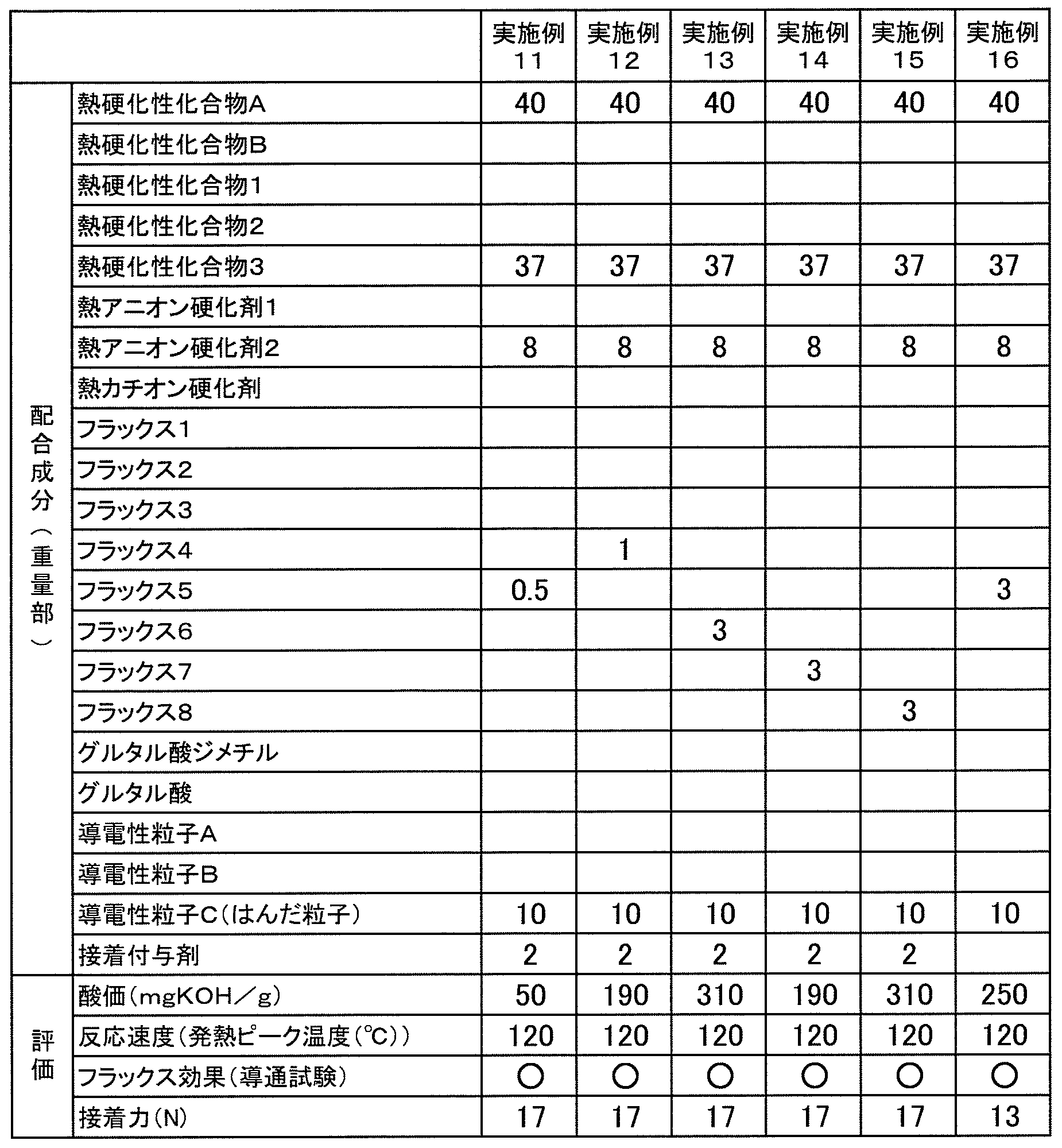
- Examples 1 to 16 and Comparative Examples 1 to 5 The components shown in Table 1 below were blended in the blending amounts shown in Tables 1 and 2 to obtain anisotropic conductive paste.
- connection structure A glass epoxy substrate (FR-4 substrate) having a copper electrode pattern (copper electrode thickness 10 ⁇ m) with an L / S of 100 ⁇ m / 100 ⁇ m on the upper surface was prepared. Moreover, the flexible printed circuit board which has a copper electrode pattern (copper electrode thickness 10 micrometers) with L / S of 100 micrometers / 100 micrometers on the lower surface was prepared.
- the obtained anisotropic conductive paste was applied on the upper surface of the glass epoxy substrate so as to have a thickness of 30 ⁇ m to form an anisotropic conductive paste layer.
- it heated at 70 degreeC.
- the said flexible printed circuit board was laminated
- a pressure heating head is placed on the upper surface of the flexible printed circuit board, and a pressure of 2.0 MPa is applied.
- the conductive paste layer was fully cured at 185 ° C. to obtain a connection structure.
- connection structure a 20 ⁇ m-thick polyimide resin processed to 1 cm ⁇ 4 cm was adhered to 3 cm ⁇ 3 cm of the glass epoxy resin, and the adhesive strength was measured.
Landscapes
- Chemical & Material Sciences (AREA)
- Engineering & Computer Science (AREA)
- Organic Chemistry (AREA)
- Health & Medical Sciences (AREA)
- Chemical Kinetics & Catalysis (AREA)
- Medicinal Chemistry (AREA)
- Polymers & Plastics (AREA)
- Microelectronics & Electronic Packaging (AREA)
- Manufacturing & Machinery (AREA)
- Spectroscopy & Molecular Physics (AREA)
- Physics & Mathematics (AREA)
- Dispersion Chemistry (AREA)
- Inorganic Chemistry (AREA)
- Conductive Materials (AREA)
- Compositions Of Macromolecular Compounds (AREA)
- Non-Insulated Conductors (AREA)
Abstract
Description
上記アニオン硬化性化合物は、アニオン硬化剤の作用により硬化可能であれば特に限定されない。上記アニオン硬化性化合物は1種のみが用いられてもよく、2種以上が併用されてもよい。
上記導電材料は硬化剤を含む。上記導電材料は、該硬化剤として、アニオン硬化剤を含む。上記アニオン硬化剤は、1種のみが用いられてもよく、2種以上が併用されてもよい。
上記有機酸Aは、カルボキシル基及びカルボキシル基がエステル化された官能基を有する有機酸である。上記有機酸Aは、カルボキシル基を少なくとも1つ有する。上記有機酸Aは、カルボキシル基がエステル化された官能基を少なくとも1つ有する。上記有機酸Aは、1種のみが用いられてもよく、2種以上が併用されてもよい。
上記導電性粒子は、少なくとも外表面がはんだであれば特に限定されない。上記導電性粒子は、基材粒子と該基材粒子の表面上に配置された導電層とを有し、該導電層の少なくとも外表面がはんだ層である導電性粒子であることが好ましい。上記基材粒子としては、樹脂粒子、金属粒子を除く無機粒子、有機無機ハイブリッド粒子及び金属粒子等が挙げられる。上記基材粒子は、コアシェル粒子であってもよい。上記基材粒子は、金属粒子ではない基材粒子であることが好ましく、樹脂粒子、金属粒子を除く無機粒子又は有機無機ハイブリッド粒子であることがより好ましい。上記基材粒子は、樹脂により形成された樹脂粒子であることが好ましい。電極間を接続する際には、導電性粒子を電極間に配置した後、一般的に導電性粒子を圧縮させる。基材粒子が樹脂粒子であると、圧縮により導電性粒子が変形しやすく、導電性粒子と電極との接触面積が大きくなる。このため、電極間の導通信頼性を高めることができる。接続構造体における耐熱衝撃特性をより一層高める観点からは、上記導電性粒子は、樹脂粒子と該樹脂粒子の表面上に配置された導電層とを有し、該導電層の少なくとも外表面がはんだ層である導電性粒子であることが好ましい。
本発明に係る導電材料は、フレキシブルプリント基板とガラスエポキシ基板との接続(FOB(Film on Board))、又はフレキシブルプリント基板とフレキシブルプリント基板との接続(FOF(Film on Film))に好適に用いられる。
本発明に係る導電材料は、フリップチップ用途に好適に用いられる。
本発明に係る導電材料は、半導体チップとフレキシブルプリント基板との接続(COF(Chip on Film))に好適に用いられる。
上記導電材料は、フィラーを含むことが好ましい。フィラーの使用により、導電材料の硬化物の熱線膨張率を抑制できる。上記フィラーの具体例としては、シリカ、窒化アルミニウム、アルミナ、ガラス、窒化ボロン、窒化ケイ素、シリコーン、カーボン、グラファイト、グラフェン及びタルク等が挙げられる。フィラーは1種のみが用いられてもよく、2種以上が併用されてもよい。熱伝導率が高いフィラーを用いると、本硬化時間が短くなる。
本発明に係る導電材料は、ペースト状又はフィルム状の導電材料であり、ペースト状の導電材料であることが好ましい。ペースト状の導電材料は、導電ペーストである。フィルム状の導電材料は、導電フィルムである。導電材料が導電フィルムである場合、導電性粒子を含む導電フィルムに、導電性粒子を含まないフィルムが積層されてもよい。本発明に係る導電材料は、異方性導電材料であることが好ましい。本発明に係る導電材料は、電極間の接続に用いられることが好ましく、回路接続材料であることが好ましく、電極間の電気的な接続に用いられる回路接続材料であることが更に好ましい。
熱硬化性化合物A(ダイセル・オルネクス社製「EBECRYL3708」)
熱硬化性化合物B(ダイセル・オルネクス社製「EBECRYL3603」)
熱硬化性化合物1(ビスフェノールA型エポキシ化合物、三菱化学社製「YL980」)
熱硬化性化合物2(レゾルシノール型エポキシ化合物、ナガセケムテックス社製「EX-201」)
熱硬化性化合物3(エポキシ樹脂、DIC社製「EXA-4850-150」)
熱アニオン硬化剤1(旭化成社製「HX-3722」)
熱アニオン硬化剤2(旭化成社製「HX-3922」)
熱カチオン硬化剤(三新化学社製「SI-60」)
フラックス1(グルタル酸85重量%とグルタル酸メチル5重量%とグルタル酸ジメチル10重量%とを含む(グルタル酸とメタノールとを錫触媒にて反応させた反応物)、エステル化率12.5%)
フラックス2(グルタル酸50重量%とグルタル酸メチル35重量%とグルタル酸ジメチル15重量%とを含む(グルタル酸とメタノールとを錫触媒にて反応させた反応物)、エステル化率32.5%)
フラックス3(グルタル酸10重量%とグルタル酸メチル20重量%とグルタル酸ジメチル70重量%とを含む(グルタル酸とメタノールとを錫触媒にて反応させた反応物)、エステル化率80%)
フラックス4(グルタル酸5重量%とグルタル酸メチル10重量%とグルタル酸ジメチル85重量%とを含む(グルタル酸とメタノールとを錫触媒にて反応させた反応物)、エステル化率90%)
フラックス5(テレフタル酸40重量%とテレフタル酸メチル30重量%とテレフタル酸ジメチル30重量%とを含む(テレフタル酸とメタノールとを錫触媒にて反応させた反応物)、エステル化率45%)
フラックス6(グルタル酸メチル100重量%(グルタル酸とメタノールとを錫触媒にて反応させた反応物の分離精製物)、エステル化率50%)
フラックス7(グルタル酸40重量%とグルタル酸メチル60重量%とを含む(グルタル酸とグルタル酸メチルとを混合した混合物)、エステル化率30%)
フラックス8(グルタル酸メチル90重量%とグルタル酸ジメチル10重量%とを含む(グルタル酸メチルとグルタル酸ジメチルとを混合した混合物)、エステル化率50%)
グルタル酸ジメチル
グルタル酸
導電性粒子A:ジビニルベンゼン樹脂粒子の表面にニッケルめっき層が形成されており、かつ該ニッケルめっき層の表面に金めっき層が形成されている金属層を有する導電性粒子A(平均粒子径15μm)
導電性粒子B:ジビニルベンゼン樹脂粒子の表面上に銅層が形成されており、該銅層の表面にはんだ層が形成されている導電性粒子B
[導電性粒子Bの作製方法]
平均粒子径10μmのジビニルベンゼン樹脂粒子(積水化学工業社製「ミクロパールSP-210」)を無電解ニッケルめっきし、樹脂粒子の表面上に厚さ0.1μmの下地ニッケルめっき層を形成した。次いで、下地ニッケルめっき層が形成された樹脂粒子を電解銅めっきし、厚さ1μmの銅層を形成した。更に、錫及びビスマスを含有する電解めっき液を用いて、電解めっきし、厚さ1μmのはんだ層を形成した。このようにして、樹脂粒子の表面上に厚み1μmの銅層が形成されており、該銅層の表面に厚み1μmのはんだ層(錫:ビスマス=43重量%:57重量%)が形成されている導電性粒子Bを作製した。
導電性粒子C:SnBiはんだ粒子(三井金属社製「DS-10」、平均粒子径(メディアン径)12μm)
接着付与剤(信越化学工業社製「KBE-403」)
下記の表1に示す成分を下記の表1,2に示す配合量で配合して、異方性導電ペーストを得た。
L/Sが100μm/100μmの銅電極パターン(銅電極厚み10μm)を上面に有するガラスエポキシ基板(FR-4基板)を用意した。また、L/Sが100μm/100μmの銅電極パターン(銅電極厚み10μm)を下面に有するフレキシブルプリント基板を用意した。
(1)酸価
得られた異方性導電ペーストにおいて、エタノール100mLに有機酸1gと、フェノールフタレン1滴とを入れ、1N-KOHで滴定をすることで、酸価を計算した。
得られた異方性導電ペーストにおいて、DSCで発熱ピーク温度を測定して、比較した。
得られた接続構造体の上下の電極間の接続抵抗をそれぞれ、4端子法により測定した。2つの接続抵抗の平均値を算出した。なお、電圧=電流×抵抗の関係から、一定の電流を流した時の電圧を測定することにより接続抵抗を求めることができる。上下の電極間の導通試験を下記の基準で判定した。
○○:接続抵抗の平均値が8.0Ω以下
○:接続抵抗の平均値が8.0Ωを超え、10.0Ω以下
△:接続抵抗の平均値が10.0Ωを超え、15.0Ω以下
×接続抵抗の平均値が15.0Ωを超える
得られた接続構造体において、ガラスエポキシ樹脂3cm×3cmに対して1cm×4cmに加工した厚み20μmのポリイミド樹脂を接着して接着力の測定を行った。

1a…表面
2…樹脂粒子
2a…表面
3…導電層
4…第1の導電層
4a…表面
5…はんだ層
5a…溶融したはんだ層部分
11…導電性粒子
12…はんだ層
16…はんだ粒子
21…接続構造体
22…第1の接続対象部材
22a…表面
22b…第1の電極
23…第2の接続対象部材
23a…表面
23b…第2の電極
24…接続部
Claims (11)
- 少なくとも外表面がはんだである導電性粒子と、
アニオン硬化性化合物と、
アニオン硬化剤と、
カルボキシル基及びカルボキシル基がエステル化された官能基を有する有機酸とを含む、導電材料。 - 前記カルボキシル基及びカルボキシル基がエステル化された官能基を有する有機酸は、カルボキシル基を複数有する有機酸におけるカルボキシル基の一部をエステル化することで得られる、請求項1に記載の導電材料。
- 前記カルボキシル基及びカルボキシル基がエステル化された官能基を有する有機酸は、前記カルボキシル基を複数有する有機酸とアルコールとを、カルボキシル基の一部をエステル化するように反応させて得られる、請求項1又は2に記載の導電材料。
- カルボキシル基を複数有する有機酸におけるカルボキシル基の全部をエステル化することで得られるエステル化物をさらに含む、請求項1~3のいずれか1項に記載の導電材料。
- カルボキシル基を複数有し、かつカルボキシル基がエステル化された官能基を有さない有機酸をさらに含む、請求項1~3のいずれか1項に記載の導電材料。
- カルボキシル基を複数有する有機酸におけるカルボキシル基の全部をエステル化することで得られるエステル化物と、カルボキシル基を複数有し、かつカルボキシル基がエステル化された官能基を有さない有機酸とをさらに含む、請求項1~3のいずれか1項に記載の導電材料。
- 前記カルボキシル基及びカルボキシル基がエステル化された官能基を有する有機酸と、カルボキシル基を複数有する有機酸におけるカルボキシル基の全部をエステル化することで得られるエステル化物と、カルボキシル基を複数有し、かつカルボキシル基がエステル化された官能基を有さない有機酸との全体において、カルボキシル基とカルボキシル基がエステル化された官能基との全個数100%中、カルボキシル基がエステル化された官能基の割合が10%以上、80%以下である、請求項6に記載の導電材料。
- 酸価が50mgKOH/g以上、370mgKOH/g以下である、請求項1~7のいずれか1項に記載の導電材料。
- 前記カルボキシル基及びカルボキシル基がエステル化された官能基を有する有機酸が、カルボキシル基を1個有する、請求項1~8のいずれか1項に記載の導電材料。
- 電極間の電気的な接続に用いられる回路接続材料である、請求項1~9のいずれか1項に記載の導電材料。
- 第1の電極を表面に有する第1の接続対象部材と、
第2の電極を表面に有する第2の接続対象部材と、
前記第1の接続対象部材と前記第2の接続対象部材とを接続している接続部とを備え、
前記接続部が、請求項1~10のいずれか1項に記載の導電材料により形成されており、
前記第1の電極と前記第2の電極とが前記導電性粒子により電気的に接続されている、接続構造体。
Priority Applications (4)
| Application Number | Priority Date | Filing Date | Title |
|---|---|---|---|
| CN201480003151.0A CN104822773B (zh) | 2013-05-23 | 2014-05-20 | 导电材料及连接结构体 |
| JP2014541463A JP5735716B2 (ja) | 2013-05-23 | 2014-05-20 | 導電材料及び接続構造体 |
| KR1020157011057A KR101579712B1 (ko) | 2013-05-23 | 2014-05-20 | 도전 재료 및 접속 구조체 |
| US14/891,615 US9490046B2 (en) | 2013-05-23 | 2014-05-20 | Conductive material and connected structure |
Applications Claiming Priority (2)
| Application Number | Priority Date | Filing Date | Title |
|---|---|---|---|
| JP2013-109137 | 2013-05-23 | ||
| JP2013109137 | 2013-05-23 |
Publications (1)
| Publication Number | Publication Date |
|---|---|
| WO2014189028A1 true WO2014189028A1 (ja) | 2014-11-27 |
Family
ID=51933581
Family Applications (1)
| Application Number | Title | Priority Date | Filing Date |
|---|---|---|---|
| PCT/JP2014/063290 Ceased WO2014189028A1 (ja) | 2013-05-23 | 2014-05-20 | 導電材料及び接続構造体 |
Country Status (6)
| Country | Link |
|---|---|
| US (1) | US9490046B2 (ja) |
| JP (1) | JP5735716B2 (ja) |
| KR (1) | KR101579712B1 (ja) |
| CN (1) | CN104822773B (ja) |
| TW (1) | TWI523047B (ja) |
| WO (1) | WO2014189028A1 (ja) |
Cited By (4)
| Publication number | Priority date | Publication date | Assignee | Title |
|---|---|---|---|---|
| CN106661347A (zh) * | 2014-12-17 | 2017-05-10 | 积水化学工业株式会社 | 光固化性组合物及电子部件的制造方法 |
| EP3185248A1 (en) * | 2015-12-23 | 2017-06-28 | Heraeus Deutschland GmbH & Co. KG | Process for electrically contacting a coated lead with a particle |
| WO2020189697A1 (ja) * | 2019-03-19 | 2020-09-24 | 積水化学工業株式会社 | 樹脂粒子、導電性粒子、導電材料及び接続構造体 |
| WO2022224934A1 (ja) * | 2021-04-19 | 2022-10-27 | 昭和電工マテリアルズ株式会社 | 接着剤組成物及び接続構造体の製造方法 |
Families Citing this family (8)
| Publication number | Priority date | Publication date | Assignee | Title |
|---|---|---|---|---|
| TWI682238B (zh) * | 2014-07-04 | 2020-01-11 | 日商積水化學工業股份有限公司 | 光硬化性組合物及電子零件之製造方法 |
| JP6524780B2 (ja) * | 2015-04-20 | 2019-06-05 | セイコーエプソン株式会社 | 電気配線部材の製造方法、電気配線部材形成用材料、電気配線部材、電気配線基板の製造方法、電気配線基板形成用材料、電気配線基板、振動子、電子機器および移動体 |
| US9966480B2 (en) | 2015-04-28 | 2018-05-08 | Samsung Sdi Co., Ltd. | Electrode composition, electrode manufactured using the same, and solar cell |
| WO2017029993A1 (ja) * | 2015-08-19 | 2017-02-23 | 積水化学工業株式会社 | 導電材料及び接続構造体 |
| JP6966322B2 (ja) * | 2016-01-25 | 2021-11-17 | 積水化学工業株式会社 | 導電材料及び接続構造体 |
| KR101877931B1 (ko) * | 2016-12-06 | 2018-07-12 | 주식회사 테토스 | 솔더 입자의 제조 방법 |
| JPWO2018147424A1 (ja) * | 2017-02-13 | 2019-12-12 | タツタ電線株式会社 | プリント配線板 |
| CN116871515B (zh) * | 2023-06-13 | 2024-10-11 | 上海银浆科技有限公司 | 银/石墨烯双壳包覆铜粉、制备方法及导电浆料 |
Citations (9)
| Publication number | Priority date | Publication date | Assignee | Title |
|---|---|---|---|---|
| JP2003225795A (ja) * | 2002-01-30 | 2003-08-12 | Showa Denko Kk | ハンダ付け用フラックスおよびハンダペースト |
| WO2006064849A1 (ja) * | 2004-12-15 | 2006-06-22 | Tamurakaken Corporation | 導電性接着剤、これを用いた導電部及び電子部品モジュール |
| JP2008012576A (ja) * | 2006-07-07 | 2008-01-24 | Fuji Electric Holdings Co Ltd | ソルダーペースト組成物及びそれを用いたプリント配線基板への電子部品実装方法 |
| JP2009242716A (ja) * | 2008-03-31 | 2009-10-22 | Panasonic Electric Works Co Ltd | 熱硬化性樹脂組成物及びその製造方法 |
| JP2009263500A (ja) * | 2008-04-24 | 2009-11-12 | Panasonic Electric Works Co Ltd | 熱硬化性樹脂組成物及びその製造方法 |
| JP2009263499A (ja) * | 2008-04-24 | 2009-11-12 | Panasonic Electric Works Co Ltd | 熱硬化性樹脂組成物及びその製造方法 |
| JP2011016967A (ja) * | 2009-07-10 | 2011-01-27 | Panasonic Electric Works Co Ltd | 熱硬化性樹脂組成物及び回路基板 |
| WO2012102079A1 (ja) * | 2011-01-27 | 2012-08-02 | 日立化成工業株式会社 | 導電性接着剤組成物、接続体及び太陽電池モジュール |
| JP2012216770A (ja) * | 2011-03-30 | 2012-11-08 | Tamura Seisakusho Co Ltd | 異方性導電性ペーストおよびそれを用いた電子部品の接続方法 |
Family Cites Families (9)
| Publication number | Priority date | Publication date | Assignee | Title |
|---|---|---|---|---|
| JPH084953B2 (ja) | 1991-04-17 | 1996-01-24 | ユーホーケミカル株式会社 | フラックス又ははんだペースト用腐食防止剤 |
| US5837119A (en) * | 1995-03-31 | 1998-11-17 | International Business Machines Corporation | Methods of fabricating dendritic powder materials for high conductivity paste applications |
| JP3378139B2 (ja) | 1996-03-19 | 2003-02-17 | 株式会社デンソー | はんだ付け用のフラックス |
| JP3785435B2 (ja) | 1998-08-27 | 2006-06-14 | 株式会社デンソー | はんだペーストおよび表面実装型電子装置 |
| JP2005203497A (ja) * | 2004-01-14 | 2005-07-28 | Toshiba Corp | 半導体装置およびその製造方法 |
| JP2006199937A (ja) | 2004-12-15 | 2006-08-03 | Tamura Kaken Co Ltd | 導電性接着剤、これを用いた導電部及び電子部品モジュール |
| EP2357876A4 (en) * | 2008-09-05 | 2012-04-25 | Sumitomo Bakelite Co | Electroconductive connecting material, method for connecting terminals to each other using the electroconductive connecting material, and method for manufacturing connecting terminal |
| US20120183781A1 (en) * | 2009-09-30 | 2012-07-19 | Sumitomo Bakelite Co., Ltd. | Conductive connecting material, method for connecting terminals and method for producing connection terminal |
| CN102737752B (zh) * | 2011-03-30 | 2016-06-29 | 株式会社田村制作所 | 各向异性导电糊以及使用该导电糊的电子部件的连接方法 |
-
2014
- 2014-05-20 KR KR1020157011057A patent/KR101579712B1/ko active Active
- 2014-05-20 JP JP2014541463A patent/JP5735716B2/ja active Active
- 2014-05-20 WO PCT/JP2014/063290 patent/WO2014189028A1/ja not_active Ceased
- 2014-05-20 US US14/891,615 patent/US9490046B2/en active Active
- 2014-05-20 CN CN201480003151.0A patent/CN104822773B/zh active Active
- 2014-05-23 TW TW103118153A patent/TWI523047B/zh active
Patent Citations (9)
| Publication number | Priority date | Publication date | Assignee | Title |
|---|---|---|---|---|
| JP2003225795A (ja) * | 2002-01-30 | 2003-08-12 | Showa Denko Kk | ハンダ付け用フラックスおよびハンダペースト |
| WO2006064849A1 (ja) * | 2004-12-15 | 2006-06-22 | Tamurakaken Corporation | 導電性接着剤、これを用いた導電部及び電子部品モジュール |
| JP2008012576A (ja) * | 2006-07-07 | 2008-01-24 | Fuji Electric Holdings Co Ltd | ソルダーペースト組成物及びそれを用いたプリント配線基板への電子部品実装方法 |
| JP2009242716A (ja) * | 2008-03-31 | 2009-10-22 | Panasonic Electric Works Co Ltd | 熱硬化性樹脂組成物及びその製造方法 |
| JP2009263500A (ja) * | 2008-04-24 | 2009-11-12 | Panasonic Electric Works Co Ltd | 熱硬化性樹脂組成物及びその製造方法 |
| JP2009263499A (ja) * | 2008-04-24 | 2009-11-12 | Panasonic Electric Works Co Ltd | 熱硬化性樹脂組成物及びその製造方法 |
| JP2011016967A (ja) * | 2009-07-10 | 2011-01-27 | Panasonic Electric Works Co Ltd | 熱硬化性樹脂組成物及び回路基板 |
| WO2012102079A1 (ja) * | 2011-01-27 | 2012-08-02 | 日立化成工業株式会社 | 導電性接着剤組成物、接続体及び太陽電池モジュール |
| JP2012216770A (ja) * | 2011-03-30 | 2012-11-08 | Tamura Seisakusho Co Ltd | 異方性導電性ペーストおよびそれを用いた電子部品の接続方法 |
Cited By (8)
| Publication number | Priority date | Publication date | Assignee | Title |
|---|---|---|---|---|
| CN106661347A (zh) * | 2014-12-17 | 2017-05-10 | 积水化学工业株式会社 | 光固化性组合物及电子部件的制造方法 |
| EP3185248A1 (en) * | 2015-12-23 | 2017-06-28 | Heraeus Deutschland GmbH & Co. KG | Process for electrically contacting a coated lead with a particle |
| WO2020189697A1 (ja) * | 2019-03-19 | 2020-09-24 | 積水化学工業株式会社 | 樹脂粒子、導電性粒子、導電材料及び接続構造体 |
| JPWO2020189697A1 (ja) * | 2019-03-19 | 2020-09-24 | ||
| JP7411553B2 (ja) | 2019-03-19 | 2024-01-11 | 積水化学工業株式会社 | 樹脂粒子、導電性粒子、導電材料及び接続構造体 |
| US11884782B2 (en) | 2019-03-19 | 2024-01-30 | Sekisui Chemical Co., Ltd. | Resin particles, conductive particles, conductive material and connection structure |
| JP2024038074A (ja) * | 2019-03-19 | 2024-03-19 | 積水化学工業株式会社 | 樹脂粒子、導電性粒子、導電材料及び接続構造体 |
| WO2022224934A1 (ja) * | 2021-04-19 | 2022-10-27 | 昭和電工マテリアルズ株式会社 | 接着剤組成物及び接続構造体の製造方法 |
Also Published As
| Publication number | Publication date |
|---|---|
| US9490046B2 (en) | 2016-11-08 |
| US20160086687A1 (en) | 2016-03-24 |
| KR20150117633A (ko) | 2015-10-20 |
| JPWO2014189028A1 (ja) | 2017-02-23 |
| KR101579712B1 (ko) | 2015-12-22 |
| TWI523047B (zh) | 2016-02-21 |
| CN104822773A (zh) | 2015-08-05 |
| JP5735716B2 (ja) | 2015-06-17 |
| TW201503170A (zh) | 2015-01-16 |
| CN104822773B (zh) | 2017-09-22 |
Similar Documents
| Publication | Publication Date | Title |
|---|---|---|
| JP5735716B2 (ja) | 導電材料及び接続構造体 | |
| CN103443869B (zh) | 导电性粒子、导电性粒子的制造方法、导电材料及连接结构体 | |
| KR101380454B1 (ko) | 도전 재료 및 접속 구조체 | |
| JP6152043B2 (ja) | 導電材料及び接続構造体 | |
| JP2014017248A (ja) | 導電材料、導電材料の製造方法及び接続構造体 | |
| CN104540869A (zh) | 电子部件用固化性组合物、连接结构体及连接结构体的制造方法 | |
| JP6496431B2 (ja) | 導電材料及び接続構造体 | |
| JP5613220B2 (ja) | 電子部品接続材料及び接続構造体 | |
| WO2017130892A1 (ja) | 導電材料及び接続構造体 | |
| JP6328996B2 (ja) | 導電ペースト、接続構造体及び接続構造体の製造方法 | |
| JP2016004971A (ja) | 接続構造体及び接続構造体の製造方法 | |
| JP6600234B2 (ja) | 導電材料及び接続構造体 | |
| JP2017045541A (ja) | 導電材料及び接続構造体 | |
| JP2017045607A (ja) | 導電材料、接続構造体及び接続構造体の製造方法 | |
| JP6329014B2 (ja) | 接続構造体及び接続構造体の製造方法 | |
| WO2017010445A1 (ja) | 導電材料及び接続構造体 | |
| JP2018060786A (ja) | 導電材料及び接続構造体 | |
| JP6533427B2 (ja) | 導電材料及び接続構造体 | |
| WO2017033931A1 (ja) | 導電材料及び接続構造体 | |
| JP2015008131A (ja) | 導電材料及び接続構造体 | |
| JP2017045606A (ja) | 導電材料、接続構造体及び接続構造体の製造方法 | |
| JP2020170592A (ja) | 導電材料及び接続構造体 | |
| JP2017022099A (ja) | 導電材料及び接続構造体 | |
| JP2017045543A (ja) | 導電材料及び接続構造体 |
Legal Events
| Date | Code | Title | Description |
|---|---|---|---|
| ENP | Entry into the national phase |
Ref document number: 2014541463 Country of ref document: JP Kind code of ref document: A |
|
| 121 | Ep: the epo has been informed by wipo that ep was designated in this application |
Ref document number: 14800729 Country of ref document: EP Kind code of ref document: A1 |
|
| ENP | Entry into the national phase |
Ref document number: 20157011057 Country of ref document: KR Kind code of ref document: A |
|
| WWE | Wipo information: entry into national phase |
Ref document number: 14891615 Country of ref document: US |
|
| NENP | Non-entry into the national phase |
Ref country code: DE |
|
| 122 | Ep: pct application non-entry in european phase |
Ref document number: 14800729 Country of ref document: EP Kind code of ref document: A1 |