WO2014185472A1 - 表示装置およびテレビジョン受像機 - Google Patents
表示装置およびテレビジョン受像機 Download PDFInfo
- Publication number
- WO2014185472A1 WO2014185472A1 PCT/JP2014/062887 JP2014062887W WO2014185472A1 WO 2014185472 A1 WO2014185472 A1 WO 2014185472A1 JP 2014062887 W JP2014062887 W JP 2014062887W WO 2014185472 A1 WO2014185472 A1 WO 2014185472A1
- Authority
- WO
- WIPO (PCT)
- Prior art keywords
- substrate
- display device
- back cabinet
- rib
- led
- Prior art date
- Legal status (The legal status is an assumption and is not a legal conclusion. Google has not performed a legal analysis and makes no representation as to the accuracy of the status listed.)
- Ceased
Links
Images














Classifications
-
- F—MECHANICAL ENGINEERING; LIGHTING; HEATING; WEAPONS; BLASTING
- F21—LIGHTING
- F21V—FUNCTIONAL FEATURES OR DETAILS OF LIGHTING DEVICES OR SYSTEMS THEREOF; STRUCTURAL COMBINATIONS OF LIGHTING DEVICES WITH OTHER ARTICLES, NOT OTHERWISE PROVIDED FOR
- F21V17/00—Fastening of component parts of lighting devices, e.g. shades, globes, refractors, reflectors, filters, screens, grids or protective cages
- F21V17/10—Fastening of component parts of lighting devices, e.g. shades, globes, refractors, reflectors, filters, screens, grids or protective cages characterised by specific fastening means or way of fastening
-
- F—MECHANICAL ENGINEERING; LIGHTING; HEATING; WEAPONS; BLASTING
- F21—LIGHTING
- F21V—FUNCTIONAL FEATURES OR DETAILS OF LIGHTING DEVICES OR SYSTEMS THEREOF; STRUCTURAL COMBINATIONS OF LIGHTING DEVICES WITH OTHER ARTICLES, NOT OTHERWISE PROVIDED FOR
- F21V29/00—Protecting lighting devices from thermal damage; Cooling or heating arrangements specially adapted for lighting devices or systems
- F21V29/50—Cooling arrangements
- F21V29/70—Cooling arrangements characterised by passive heat-dissipating elements, e.g. heat-sinks
-
- G—PHYSICS
- G02—OPTICS
- G02F—OPTICAL DEVICES OR ARRANGEMENTS FOR THE CONTROL OF LIGHT BY MODIFICATION OF THE OPTICAL PROPERTIES OF THE MEDIA OF THE ELEMENTS INVOLVED THEREIN; NON-LINEAR OPTICS; FREQUENCY-CHANGING OF LIGHT; OPTICAL LOGIC ELEMENTS; OPTICAL ANALOGUE/DIGITAL CONVERTERS
- G02F1/00—Devices or arrangements for the control of the intensity, colour, phase, polarisation or direction of light arriving from an independent light source, e.g. switching, gating or modulating; Non-linear optics
- G02F1/01—Devices or arrangements for the control of the intensity, colour, phase, polarisation or direction of light arriving from an independent light source, e.g. switching, gating or modulating; Non-linear optics for the control of the intensity, phase, polarisation or colour
- G02F1/13—Devices or arrangements for the control of the intensity, colour, phase, polarisation or direction of light arriving from an independent light source, e.g. switching, gating or modulating; Non-linear optics for the control of the intensity, phase, polarisation or colour based on liquid crystals, e.g. single liquid crystal display cells
- G02F1/133—Constructional arrangements; Operation of liquid crystal cells; Circuit arrangements
- G02F1/1333—Constructional arrangements; Manufacturing methods
- G02F1/1335—Structural association of cells with optical devices, e.g. polarisers or reflectors
- G02F1/1336—Illuminating devices
- G02F1/133602—Direct backlight
- G02F1/133608—Direct backlight including particular frames or supporting means
-
- H—ELECTRICITY
- H04—ELECTRIC COMMUNICATION TECHNIQUE
- H04N—PICTORIAL COMMUNICATION, e.g. TELEVISION
- H04N5/00—Details of television systems
- H04N5/64—Constructional details of receivers, e.g. cabinets or dust covers
-
- G—PHYSICS
- G02—OPTICS
- G02F—OPTICAL DEVICES OR ARRANGEMENTS FOR THE CONTROL OF LIGHT BY MODIFICATION OF THE OPTICAL PROPERTIES OF THE MEDIA OF THE ELEMENTS INVOLVED THEREIN; NON-LINEAR OPTICS; FREQUENCY-CHANGING OF LIGHT; OPTICAL LOGIC ELEMENTS; OPTICAL ANALOGUE/DIGITAL CONVERTERS
- G02F1/00—Devices or arrangements for the control of the intensity, colour, phase, polarisation or direction of light arriving from an independent light source, e.g. switching, gating or modulating; Non-linear optics
- G02F1/01—Devices or arrangements for the control of the intensity, colour, phase, polarisation or direction of light arriving from an independent light source, e.g. switching, gating or modulating; Non-linear optics for the control of the intensity, phase, polarisation or colour
- G02F1/13—Devices or arrangements for the control of the intensity, colour, phase, polarisation or direction of light arriving from an independent light source, e.g. switching, gating or modulating; Non-linear optics for the control of the intensity, phase, polarisation or colour based on liquid crystals, e.g. single liquid crystal display cells
- G02F1/133—Constructional arrangements; Operation of liquid crystal cells; Circuit arrangements
- G02F1/1333—Constructional arrangements; Manufacturing methods
- G02F1/133308—Support structures for LCD panels, e.g. frames or bezels
- G02F1/133314—Back frames
-
- G—PHYSICS
- G02—OPTICS
- G02F—OPTICAL DEVICES OR ARRANGEMENTS FOR THE CONTROL OF LIGHT BY MODIFICATION OF THE OPTICAL PROPERTIES OF THE MEDIA OF THE ELEMENTS INVOLVED THEREIN; NON-LINEAR OPTICS; FREQUENCY-CHANGING OF LIGHT; OPTICAL LOGIC ELEMENTS; OPTICAL ANALOGUE/DIGITAL CONVERTERS
- G02F1/00—Devices or arrangements for the control of the intensity, colour, phase, polarisation or direction of light arriving from an independent light source, e.g. switching, gating or modulating; Non-linear optics
- G02F1/01—Devices or arrangements for the control of the intensity, colour, phase, polarisation or direction of light arriving from an independent light source, e.g. switching, gating or modulating; Non-linear optics for the control of the intensity, phase, polarisation or colour
- G02F1/13—Devices or arrangements for the control of the intensity, colour, phase, polarisation or direction of light arriving from an independent light source, e.g. switching, gating or modulating; Non-linear optics for the control of the intensity, phase, polarisation or colour based on liquid crystals, e.g. single liquid crystal display cells
- G02F1/133—Constructional arrangements; Operation of liquid crystal cells; Circuit arrangements
- G02F1/1333—Constructional arrangements; Manufacturing methods
- G02F1/133382—Heating or cooling of liquid crystal cells other than for activation, e.g. circuits or arrangements for temperature control, stabilisation or uniform distribution over the cell
- G02F1/133385—Heating or cooling of liquid crystal cells other than for activation, e.g. circuits or arrangements for temperature control, stabilisation or uniform distribution over the cell with cooling means, e.g. fans
-
- G—PHYSICS
- G02—OPTICS
- G02F—OPTICAL DEVICES OR ARRANGEMENTS FOR THE CONTROL OF LIGHT BY MODIFICATION OF THE OPTICAL PROPERTIES OF THE MEDIA OF THE ELEMENTS INVOLVED THEREIN; NON-LINEAR OPTICS; FREQUENCY-CHANGING OF LIGHT; OPTICAL LOGIC ELEMENTS; OPTICAL ANALOGUE/DIGITAL CONVERTERS
- G02F1/00—Devices or arrangements for the control of the intensity, colour, phase, polarisation or direction of light arriving from an independent light source, e.g. switching, gating or modulating; Non-linear optics
- G02F1/01—Devices or arrangements for the control of the intensity, colour, phase, polarisation or direction of light arriving from an independent light source, e.g. switching, gating or modulating; Non-linear optics for the control of the intensity, phase, polarisation or colour
- G02F1/13—Devices or arrangements for the control of the intensity, colour, phase, polarisation or direction of light arriving from an independent light source, e.g. switching, gating or modulating; Non-linear optics for the control of the intensity, phase, polarisation or colour based on liquid crystals, e.g. single liquid crystal display cells
- G02F1/133—Constructional arrangements; Operation of liquid crystal cells; Circuit arrangements
- G02F1/1333—Constructional arrangements; Manufacturing methods
- G02F1/1335—Structural association of cells with optical devices, e.g. polarisers or reflectors
- G02F1/1336—Illuminating devices
- G02F1/133602—Direct backlight
- G02F1/133603—Direct backlight with LEDs
Definitions
- the present invention relates to a display device and a television receiver including the display device.
- Patent Document 1 includes, as a technique for fixing a plate member with ribs formed on a housing, an attachment portion for attaching the plate member, and a plurality of ribs provided on the attachment portion and locking the plate member.
- the plurality of ribs include a first rib that locks one side portion of the plate member and a second rib that locks the other side portion of the plate member.
- a stop structure is described.
- Japanese Patent Publication “JP 2009-181037 A (published on August 13, 2009)” Japanese Patent Publication “Japanese Patent Laid-Open No. 2008-136076” (published on June 12, 2008) Japanese Patent Publication “JP 2009-69532 A (published on April 2, 2009)” Japanese Patent Publication “JP 2009-267008 A (published on November 12, 2009)”
- the present inventors are examining a display device in which the substrate on which the light source is arranged is fixed to the back cabinet instead of the back chassis.
- a display device is preferably configured so that the substrate does not bend.
- Patent Document 1 it is necessary to bend the plate member when fixing the plate member to the rib. Therefore, it is difficult to apply the technique of Patent Document 1 to the display device.
- the present invention has been made in view of the above problems, and in a display device in which a substrate on which a light source is arranged is fixed to a back cabinet, the substrate is made into the back cabinet in a simple process without bending the substrate.
- the main purpose is to provide technology for fixing.
- a display device includes a back cabinet that covers a back surface of the device, a light source that is fixed to the back cabinet, and is disposed on a surface opposite to the back cabinet.
- a fixing rib for fixing the substrate is formed in the back cabinet, and the fixing rib loosely fits the substrate to the fixing rib, When the substrate is moved to a fixing position along the longitudinal direction of the substrate, the substrate is fixed, and the fixing rib protrudes toward an end portion in the short direction of the substrate.
- a protrusion is provided, and a first notch that fits into the first protrusion when the substrate is moved to the fixed position is provided at an end in a short direction of the substrate. It is said.
- the fixing rib provided in the back cabinet loosely fits the substrate to the fixing rib,
- the substrate is fixed when the substrate is moved to the fixing position along the longitudinal direction, and the first protrusion of the fixing rib is provided at the end in the short direction of the substrate when the substrate is moved to the fixing position.
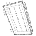
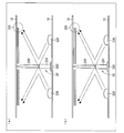
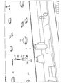
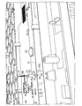
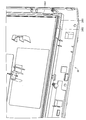
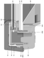
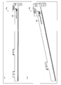
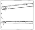
- FIG. 1 is an exploded perspective view schematically showing a schematic configuration of a display device according to an embodiment of the present invention. It is a perspective view showing a schematic structure of an LED substrate and a heat spreader coupled to the LED substrate in an embodiment of the present invention, (a) shows the LED substrate and the heat spreader observed from the opposite side of the back cabinet, (B) shows what observed the LED board and the heat spreader from the back cabinet side.
- FIG. 1 It is a perspective view which shows schematic structure of the LED board and heat spreader of the state in the separated state in one Embodiment of this invention, (a) shows an LED board, (b) shows a heat spreader. It is a perspective view which shows schematic structure of the inner side of the back cabinet in one Embodiment of this invention. It is a perspective view which shows the state by which the LED board was fixed to the back cabinet in one Embodiment of this invention. It is a figure which shows partially the mode of fixation to the back cabinet of LED board in one Embodiment of this invention, (a) shows the state by which the LED board is not being fixed, (b) Indicates a fixed state.
- (a) is a perspective view which shows only a fixing rib
- (b) is an LED board a fixing rib It is a perspective view which shows the state loosely fitted by
- (c) is a perspective view which shows the state by which the LED board was fixed to the rib for fixing.
- (a) is a rib (1st protrusion) in the state by which the LED board was loosely fitted by the fixing rib.
- FIG. 1 It is a figure which shows schematic structure of the clip in one Embodiment of this invention
- (a) is a side view which shows a clip single-piece
- (b) is a perspective view which shows the state by which the clip was fixed to the LED board. is there. It is a perspective view which shows schematic arrangement
- (B) is a figure which shows the shadow which the clip in one Embodiment of this invention forms in an optical member.
- FIG. 26 is an AA cross-sectional view of the back cabinet shown in FIG. 25.
- FIG. 4 is an enlarged perspective view showing a part of a back cabinet 24 and an optical sheet group 17 according to the present embodiment. It is an enlarged view which shows a part of external appearance of the upper side P chassis which concerns on one Embodiment of this invention, (a) is a front view of an upper side P chassis, (b) is a perspective view of an upper side P chassis.
- FIG. 32 is a cross-sectional view of the display device shown in FIG. 31 taken along the line BB.
- FIG. 32 is a CC cross-sectional view of the display device shown in FIG. 31.
- FIG. 32 is a DD cross-sectional view of the display device shown in FIG. 31. It is a back perspective view of the front cabinet concerning one embodiment of the present invention. It is a front view which shows the state which has arrange
- a display device according to an embodiment of the present invention will be described with reference to FIGS.
- the display device according to the present embodiment is not limited to this, but may be a television receiver, for example.
- the technical scope of this invention is not limited to description of the following embodiment and drawing.
- FIG. 1 is an exploded perspective view schematically showing a schematic configuration of a display device 1 according to an embodiment of the present invention.
- the display device 1 is a liquid crystal display device.
- the display device 1 includes a front cabinet 10, a deco sheet 11, a lamp 12, a remote control circuit 13, a bezel 14, a liquid crystal panel 15, a P chassis 16, an optical sheet group 17, a diffuser plate 18, a reflective sheet 19, Clip 20, LED board 22, heat spreader 23, back cabinet 24, holder 25, bottom bracket 26, support bracket 27, main circuit 28, power supply circuit 29, stand 30, auxiliary circuit 36, button 37, speaker 38, top cover 39 and bottom A cover 40 is provided.
- the side on which the display screen exists is referred to as a front surface, and the opposite side is referred to as a back surface.
- the front cabinet 10 is a housing that mainly covers the front surface of the display device 1.
- the back cabinet 24 is a housing that mainly covers the back surface of the display device 1.
- the front cabinet 10 and the back cabinet 24 are mainly composed of an injection molded product such as plastic.
- the bezel 14 Between the front cabinet 10 and the back cabinet 24, the bezel 14, the liquid crystal panel 15, the P chassis 16, the optical sheet group 17, the diffusion plate 18, the reflection sheet 19, the LED substrate 22, and the heat spreader 23 are sequentially arranged from the front cabinet 10 side. Are overlaid and stored.
- LED substrate and heat spreader The LED substrate (substrate) 22 and the heat spreader (heat radiating plate) 23 will be described in detail with reference to FIGS.
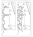
- FIG. 2 is a perspective view showing a schematic structure of the LED substrate 22 and the heat spreader 23 coupled to the LED substrate 22.
- 2A shows the LED substrate 22 and the heat spreader 23 observed from the side opposite to the back cabinet 24, and
- FIG. 2B shows the LED substrate 22 and the heat spreader 23 observed from the back cabinet 24 side. Shows what
- FIG. 3 is a plan view showing a schematic structure of the LED substrate 22 near the connector 221 and the heat spreader 23 coupled to the LED substrate 22.
- 3 (a) shows what was observed from the end side in the short direction
- FIG. 3 (b) shows what was observed from the end side in the longitudinal direction
- FIG. , What was observed from the back cabinet 24 side is shown.
- FIG. 4 is a perspective view showing a schematic structure of the LED substrate 22 near the end in the longitudinal direction opposite to the connector 221 and the heat spreader 23 coupled to the LED substrate 22.
- 4A shows what is observed from the side opposite to the back cabinet 24, and
- FIG. 4B shows what is observed from the back cabinet 24 side.
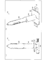
- FIG. 5 is a perspective view showing a schematic structure of the LED board 22 and the heat spreader 23 in a separated state, where (a) shows the LED board 22 and (b) shows the heat spreader 23.
- the LED substrate 22 is a substrate that is directly fixed to the back cabinet 24 without using a backlight chassis or the like, and the LED element (light source) 220 is disposed on the surface opposite to the back cabinet 24.
- the number of parts can be reduced and the assembly process can be simplified.
- the LED substrate 22 has a strip shape, and a plurality of LED elements 220 are arranged along the longitudinal direction thereof. By configuring the LED substrate 22 in this way, a plurality of LED elements 220 can be easily arranged in the display device 1.
- a connector 221 for electrically connecting to the main circuit 28 is provided at one end of the LED substrate 22 in the longitudinal direction.
- the LED board 22 is provided with a circuit for electrically connecting the connector 221 and each LED element 220 (not shown).
- the LED substrate 22 is provided with a plurality of notches and openings for functions to be described later. That is, a semicircular cutout 222 is provided at the end of the LED substrate 22 in the short direction. A semicircular cutout 223 larger than the cutout 222 is provided adjacent to the cutout 222. In addition, rectangular cutouts 226 are provided at positions corresponding to both ends of the LED substrate 22 in the short direction. In addition, an elongated opening 224 in the longitudinal direction and an elongated opening 225 in the longitudinal direction are provided in the center of the LED substrate 22 in the lateral direction.
- the heat spreader 23 is a heat radiating plate having a U-shaped short cross section, a pair of side surface portions 23a and a bottom surface portion 23b, and the bottom surface portion 23b coupled to the surface of the LED substrate 22 on the back cabinet 24 side. .
- the heat spreader 23 having a U-shaped short cross section the heat dissipation efficiency of the LED substrate 22 can be improved and the warpage of the LED substrate 22 can be suppressed with a simple configuration. That is, by making the short cross section U-shaped, it is possible to increase the surface area of the heat spreader 23 and improve the heat dissipation effect to the air. Therefore, the heat dissipation efficiency of the LED substrate 22 coupled to the heat spreader 23 Can be improved.
- the rigidity of the heat spreader 23 can be increased by making the short cross section U-shaped, warping of the LED substrate 22 coupled to the heat spreader 23 can be suppressed. Thereby, even if it is a case where the LED board 22 is directly fixed to the back cabinet 24, sufficient heat dissipation efficiency of the LED board 22 is ensured, and the curvature of the LED board 22 can be suppressed. Moreover, it also has an effect of reinforcing the strength of the back cabinet 24. Further, the heat spreader 23 can be configured to be lightweight.
- the heat spreader 23 is preferably formed of a material such as metal that has higher heat dissipation than the LED substrate 22. Thereby, the thermal radiation efficiency of LED board 22 can be improved more.
- the heat spreader 23 can be formed by SPTE.
- an opening is provided at a position corresponding to the opening provided in the LED substrate 22 in the bottom surface portion 23 b of the heat spreader 23. That is, an opening 231 having the same shape as the opening 224 is provided immediately below the opening 224 in the LED substrate 22. In addition, an opening 232 having the same shape as the opening 225 is provided immediately below the opening 225 in the LED substrate 22. An opening 233 is provided at a position adjacent to the opening 232 in the side surface portion 23 a of the heat spreader 23.
- the heat spreader 23 may be exposed on at least one end side in the longitudinal direction of the LED substrate 22. As shown in FIG. 4, in this embodiment, an exposed portion 230 of the heat spreader 23 exists at the end portion (A in the drawing) of the LED substrate 22 on the opposite side to the connector 221. By providing the exposed portion 230 in this manner, the area where the heat spreader 23 is in contact with air can be increased, and the heat dissipation efficiency can be further improved. In the exposed portion 230, a groove is formed at the center. This function will be described later.
- the heat spreader 23 and the LED substrate 22 only need to be coupled in a thermally conductive manner.
- the heat spreader 23 and the LED substrate 22 can be coupled by a heat conductive double-sided tape.
- the heat spreader 23 when configured by a conductor such as metal, the ground potential portion of the LED substrate 22 and the heat spreader 23 may be electrically connected. Accordingly, the heat spreader 23 made of a conductor can be used as a path for ground connection of the LED substrate 22, and an adverse effect that may occur when the heat spreader 23 made of a conductor is electrically floating can be avoided. it can.
- a plane light source suitable as a backlight of a liquid crystal display device can be obtained.
- the case where an LED element is used as the light source has been described as an example.
- the present invention is not limited to this, and for example, a light source other than the LED element such as a fluorescent tube is used as the light source. You may employ
- the longitudinal direction of the LED substrate 22 is parallel to the horizontal direction of the display device 1, but the present invention is not limited to this.
- the longitudinal direction of the LED substrate 22 is displayed. You may arrange
- each LED board 22 is not particularly limited.
- the short cross section of the heat spreader 23 having a U-shape indicates that the angle between the side surface portion 23a and the bottom surface portion 23b is not less than 30 degrees and not more than 150 degrees. Further, the side surface portion 23a and the bottom surface portion 23b do not have to be flat, and part or all of them may be curved surfaces.
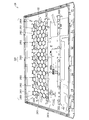
- FIG. 6 is a perspective view showing a schematic structure of the inside of the back cabinet 24 (the side on which the LED substrate 22 and the like are present).
- FIG. 7 is a perspective view showing a state in which the LED substrate 22 is fixed to the back cabinet 24. In FIG. 7, the heat spreader 23 is omitted for the sake of clarity.
- the back cabinet 24 is formed with fixing ribs 240 for fixing the LED substrate 22.
- fixing ribs 240 There are several types of fixing ribs 240 having different shapes (ribs 2400 to 2404). Details of the ribs 2400 to 2404 are shown in FIGS.
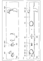
- FIG. 8 is a diagram showing a state in which the LED substrate 22 is fixed to the back cabinet 24 in the portion 2420 shown in FIG.
- FIG. 8A shows a state where the LED board 22 is not fixed
- FIG. 8B shows a state where the LED board 22 is fixed.
- FIG. 9 is a diagram illustrating a state in which the LED substrate 22 is fixed to the back cabinet 24 in the portion 2421 illustrated in FIG. 9A shows a state where the LED board 22 is not fixed, and FIG. 9B shows a state where the LED board 22 is fixed.
- FIG. 10 is a diagram showing a state in which the LED substrate 22 is fixed to the back cabinet 24 in the portion 2422 shown in FIG.
- FIG. 10A shows a state where the LED substrate 22 is not fixed
- FIG. 10B shows a state where the LED substrate 22 is fixed.
- FIG. 11 is a diagram illustrating a state in which the LED substrate 22 is fixed to the back cabinet 24 in the portion 2423 illustrated in FIG.
- FIG. 11A shows a state where the LED substrate 22 is not fixed
- FIG. 11B shows a state where the LED substrate 22 is fixed.
- FIG. 12 (a) is a perspective view showing only the fixing rib 240
- FIG. 12 (b) is a perspective view showing a state in which the LED board 22 is loosely fitted to the fixing rib 240
- 12C is a perspective view showing a state in which the LED substrate 22 is fixed to the fixing rib 240.
- the LED substrate 22 When the LED substrate 22 is fixed to the back cabinet 24, first, the LED substrate 22 is loosely fitted to the fixing rib 240 as shown in FIG. 12 (a) as shown in FIG. 12 (b). To do. In this state, the LED board 22 is movable along the longitudinal direction of the LED board 22. Then, as shown in FIG. 12C, the LED board 22 is fixed to the back cabinet 24 by moving the LED board 22 to the fixing position along the longitudinal direction of the LED board 22.
- FIG. 13 is a top view showing a detailed configuration of the rib (first protrusion) 2400.
- 13A shows a relationship between the rib 2400 and the LED board 22 in a state where the LED board 22 is loosely fitted to the fixing rib 240
- FIG. 13B shows a relation between the LED board 22 and the fixing rib 240. The relationship between the rib 2400 and the LED substrate 22 in a state fixed to 240 is shown.
- the rib 2400 protrudes toward the end of the LED substrate 22 in the short direction.
- the rib 2400 is loosely fitted to the notch (second notch) 223 of the LED board 22 and is in a freely movable state. Yes. From this state, the LED board 22 is moved along its longitudinal direction, so that the rib 2400 fits into the notch (first notch) 222 of the LED board 22 as shown in FIG.
- a force in a direction toward the outside of the LED substrate 22 (a direction indicated by a dotted arrow in the figure) is applied to the rib 2400, and a stress (a direction indicated by a solid arrow in the figure) is applied to the LED substrate 22.
- LED board 22 is fixed more firmly.
- the LED board 22 is loosely fitted to the fixing rib 240, and the LED board 22 is fixed so as to be fixed when the LED board 22 is moved to the fixing position along the longitudinal direction.
- the rib 240 is formed, the rib 2400 protruding toward the end of the LED board 22 in the short direction is formed, and moved to the fixing position at the end of the LED board 22 in the short direction A notch 222 that fits into the rib 2400 is provided.
- the LED board 22 is moved back to the fixing position along the longitudinal direction thereof, and the LED board 22 is backed by a simple process without bending the board.
- the LED board 22 can be fixed to the back cabinet.
- the LED substrate 22 is preferably provided with a notch 223 that is adjacent to the notch 222 and that is large in the notch 222 and that loosely fits into the rib 2400. Thereby, the LED board 22 can be easily loosely fitted to the fixing rib 240 without the rib 2400 interfering with the LED board 22.
- the rib 2401 includes a support portion 2401 b that supports the LED substrate 22, and a protrusion (second protrusion) 2401 a that is inserted into the opening 224 of the LED substrate 22.
- the opening 224 has an elongated shape in the longitudinal direction of the LED substrate 22 and is preferably elliptical.
- the protrusion 2401a can move freely in the longitudinal direction of the LED substrate 22, and displacement in the short direction is suppressed. Therefore, the LED substrate 22 can be prevented from moving in the other direction without preventing the LED substrate 22 from moving in the longitudinal direction. Thereby, while being able to move the LED board 22 to the longitudinal direction easily, the LED board 22 can be fixed in an exact position.
- the rib 2402 has a cylindrical shape with a notch, and supports the LED substrate 22.
- the notch of the rib 2402 is provided in a portion of the rib 2402 facing the side surface portion 23a of the heat spreader 23 coupled to the LED substrate 22. Thereby, the interference between the rib 2402 and the heat spreader 23 can be avoided.
- FIG. 14 is a side sectional view showing a detailed configuration of the rib 2403.
- the rib 2403 includes a support part (clamping part) 2403c that supports the LED board 22 and a cover part (clamping part) 2403b that holds the LED board 22 in pairs with the support part 2403c. That is, the LED substrate 22 is sandwiched between the support portion 2403c and the cover portion 2403b.
- the cover portion 2403b is inclined, and the distance between the cover portion 2403b and the LED substrate 22 is reduced as the LED substrate 22 approaches the fixed position. Thereby, in a fixed position, the support part 2403c and the cover part 2403b can clamp the LED board 22 firmly, and can fix the LED board 22 suitably.
- the rib 2403 is provided with a groove 2403a through which the side surface portion 23a of the heat spreader 23 coupled to the LED substrate 22 passes. Therefore, interference between the rib 2403 and the heat spreader 23 can be avoided, and the LED substrate 22 can be prevented from moving in the other direction without preventing the LED substrate 22 from moving in the longitudinal direction. Thereby, the LED board 22 can be fixed at an accurate position.
- the LED board 22 is provided with a notch 226 for allowing the cover portion 2403b to pass therethrough in order to loosely fit the LED board 22 to the fixing rib 240. .
- FIG. 15 is a diagram showing a detailed configuration of the rib 2404.
- FIG. 15A is a plan view of the rib 2404 observed from the side opposite to the side facing the LED substrate 22, and
- FIG. 15B shows how the LED substrate 22 is inserted into the rib 2404.
- FIG. 15A is a plan view of the rib 2404 observed from the side opposite to the side facing the LED substrate 22, and
- FIG. 15B shows how the LED substrate 22 is inserted into the rib 2404.
- the exposed portion 230 of the heat spreader 23 coupled to the LED substrate 22 is inserted into the rib 2404.
- the rib 2404 includes a pressing portion 2404a that presses the exposed portion 230 from the back cabinet 24 side, and a plate-like member that extends from the center of the pressing portion 2404a to the LED substrate 22 side. And an insertion portion 2404b to be inserted into the. Thereby, the center position of the LED substrate 22 can be correctly guided. Thereby, the LED board 22 can be fixed at an accurate position.
- the pressing portion 2404a presses and pushes up the exposed portion 230 and the end portion of the LED substrate 22, and the exposed portion 230 and the LED substrate.
- the end of 22 is pressed by the rib 2404 from the front and back. Thereby, LED board 22 is fixed more firmly.
- the rib 2404 is provided with a groove through which the side surface portion 23a of the heat spreader 23 coupled to the LED substrate 22 passes, as in the rib 2403.
- a main circuit 28 and the like are provided outside the back cabinet 24.
- a structure 2410 is provided. Therefore, on the inner side of the back cabinet 24, the depth differs depending on the position.
- the back cabinet 24 is deep. Further, in the region 2421, the back cabinet 24 is shallow. In the part 2422, the back cabinet 24 is a boundary between a deep part and a shallow part. Further, in the region 2423, the back cabinet 24 is shallow.
- the LED substrates 22 have the same height (note that the direction from the back cabinet 24 to the front cabinet 10 is upward. To do). Therefore, portions of the ribs 2401 to 2403 that function as substrate support ribs that support the LED substrate 22 that support the LED substrate 22 (support portion 2401b, top surface of the rib 2402, and support portion 2403c) are flush with each other. .
- each rib is tall in a portion 2420 where the back cabinet 24 is deep. Moreover, as shown in FIG. 9, in the part 2421 where the back cabinet 24 is shallow, each rib is short. Moreover, as shown in FIG. 10, in the site
- each LED substrate 22 Since the portions of the substrate support rib that support the LED substrate 22 are flush with each other, the height of each LED substrate 22 can be made the same. 15 can be emitted.
- the structure 2410 is provided on the bottom side of the display device of the back cabinet 24 (the lower side in the drawing in FIG. 6), it has sufficient rigidity.
- a honeycomb-like rib 2411 is formed instead of the structure 2410.
- the reflection sheet 19 is provided between the LED element 220 and the LED substrate 22 and reflects light emitted from the LED element 220.
- the reflection sheet 19 is not necessarily required, since the light absorbed by the LED substrate 22 or the back cabinet 24 can be effectively used by using the reflection sheet 19, it is emitted toward the diffusion plate 18. The amount of light can be increased. Thereby, the reflection sheet 19 can improve the luminance of the liquid crystal panel 15.
- the reflection sheet 19 is made of, for example, polyester represented by foamed PET (Polyethylene Terephthalate), and has light reflection characteristics.
- the reflective sheet 19 may be a sheet that regularly reflects incident light, but it is more preferable to use a sheet that irregularly reflects light.
- the reflection sheet 19 can reflect light including a reflection component having an angle different from the incident angle by using a sheet on which incident light is irregularly reflected.
- the clip (support column) 20 will be described in detail with reference to FIGS.
- the clip 20 is a support column that supports the diffusion plate (optical member) 18 disposed at a position facing the LED element 220.
- the clip 20 may have a tapered pin shape. Further, the clip 20 supports the diffusion plate 18 by abutting on the diffusion plate 18 from the LED element 220 side.
- FIG. 16 is a diagram showing a schematic structure of the clip 20.
- FIG. 16A is a side view showing the clip 20 alone
- FIG. 16B is a perspective view showing a state in which the clip 20 is fixed to the LED substrate 22.
- the clip 20 is the flat plate part 200 of flat plate shape, the cylindrical part 201 used as the foundation of the flat plate part 200, the collar part 202 connected to the root of the cylindrical part 201, and the collar part.
- a through-hole 203 is provided that is connected with a distance from 202.
- the clip 20 is fixed to the LED substrate 22 with the reflection sheet 19 interposed therebetween. Further, when the clip 20 is fixed to the LED substrate 22, the through portion 203 passes through the opening 225 to the opposite side of the LED substrate 22, and is paired with the flange portion 202 to form the LED substrate 22 and the reflection sheet 19. Pinch.
- the clip 20 is formed of a material having translucency.
- the clip 20 can be formed of a transparent resin.
- the flat plate part 200 is mirror-finished.
- FIG. 17 is a perspective view showing a schematic arrangement of the clip 20.
- the reflection sheet 19 is disposed on the back cabinet 24 so as to cover the LED substrate 22. Further, the LED element 220 is exposed on the reflection sheet 19. That is, the reflection sheet 19 is provided between the LED substrate 22 and the LED element 220.
- the clip 20 is fixed between two adjacent LED elements 220 (for example, the clip 20a is fixed between adjacent LED elements 220a and 220n).
- One of the plate surfaces (the mirror-finished surface) of the flat plate portion 200 is opposed to one of the two LED elements 220, and the other plate surface of the flat plate portion 200 is the other of the two LED elements 220. Opposite.
- FIG. 18 is a diagram comparing shadows formed on the diffusion plate (optical member) 18 by the clip 20 ′ according to the prior art and the clip 20 according to the present embodiment.
- FIG. 18A is a diagram showing a shadow formed on the diffusion plate 18 by the clip 20 ′ according to the prior art
- FIG. 18B is a diagram showing the clip 20 formed on the diffusion plate 18 according to the present embodiment. It is a figure which shows the shadow to do.
- the conventional clip 20 ' includes a flat plate portion 200', a cylindrical portion 201 ', and a flange portion 202'.
- the flat plate portion 200 ′ is highly glossy white for improving the light reflectivity, and has a rough surface for diffusing light.
- the clip 20 when the clip 20 according to the present embodiment is used, the light from the LED element 220 on the left side of the paper is applied to the portion 205 of the diffusion plate 18 by the clip 20 ′. And (ii) the light reflected from the LED 20 on the right side of the paper overlaps with the reflected light reflected by the clip 20.
- the clip 20 since the clip 20 has translucency, the shadow becomes weak and the flat plate portion 200 is mirror-finished, so that the reflected light becomes strong. For this reason, the shadow and the reflected light are canceled out, and no shadow remains in the portion 205.
- the clip 20 is formed on the optical member by the clip 20 by using the clip 20 having translucency and at least a part of at least a part of the two surfaces facing the LED elements 220 on both sides. Shadows can be reduced.
- the entire surface of the clip 20 is not necessarily mirror-finished in a flat plate shape. In the part where the light indicated by the dotted line in FIG. 18B does not reach, it does not have to be flat and does not have to be mirror-finished. Therefore, as shown in FIG. 18B, the clip 20 preferably includes a cylindrical portion 201 that serves as a base of the flat plate portion 200 at the lower portion of the flat plate portion 200 that is mirror-finished. Thereby, the flat plate part 200 with weak intensity
- FIG. 19 is a perspective view showing a state in which the clip 20 is fixed to the LED substrate 22.
- the LED board 22 is covered with the reflection sheet 19, only the opening 225 is visible. Further, the heat spreader 23 coupled to the LED substrate 22 is omitted.
- FIG. 20 is a perspective view showing a state in which the clip 20 is fixed to the LED substrate 22.
- the reflection sheet 19 and the heat spreader 23 are omitted.
- FIG. 21 is a plan view of the state in which the clip 20 is fixed to the LED substrate 22 as observed from the back cabinet 24 side.
- the heat spreader 23 coupled to the LED substrate 22 is omitted.
- FIG. 22 is a side view showing a state in which the clip 20 is fixed to the LED substrate 22.
- the reflection sheet 19 and the heat spreader 23 are omitted.
- the clip 20 is fixed to the LED substrate 22 to sandwich the reflective sheet 19 in pairs with the LED substrate 22. Since the clip 20 also fixes the reflective sheet 19, the assembling operation can be simplified.
- the clip 20 is only required to be fixed to the LED substrate 22, but is preferably detachably attached. As shown in FIGS. 19 to 22, the LED 20 is inserted into the LED substrate 22 and twisted to turn the LED. It is preferable to be fixed to the substrate 22.
- the penetrating portion 203 is a rod-like member that extends so as to be orthogonal to the flat plate portion 200 and the cylindrical portion 201.
- the LED board 22 is provided with an opening 225 corresponding to the penetrating portion 203 (the heat spreader 23 is also provided with an opening 232 corresponding to the opening 225 of the LED board 22). Therefore, the penetration part 203 can be penetrated to the opposite side of the LED board 22 by inserting the clip 20 into the LED board 22 in a state where the direction of the penetration part 203 and the direction of the opening 232 are matched. After that, by twisting the clip 20 by 90 degrees, for example, as shown in FIG. 21, the penetrating portion 203 functions as if it is a scissors, and the LED substrate 22 is sandwiched between the penetrating portion 203 and the collar portion 202, thereby 20 is fixed to the LED substrate 22.
- the clip 20 is simply attached to the LED substrate 22, reuse of the clip 20 and disassembly and disassembly of the display device 1 (or a direct backlight) are facilitated.
- FIG. 23 is a perspective view showing a state in which the LED substrate 22 is fixed to the back cabinet 24 and the clip 20 is fixed to the LED substrate 22.
- the portion of the LED substrate 22 to which the clip 20 is attached is supported by a rib 2402, which is a cylindrical rib having a notch.
- This part is a part where a load is applied when the clip 20 is attached.
- the cylindrical rib 2402 having a notch that supports the portion of the LED substrate 22 to which the clip 20 is attached, the LED substrate 22 is bent when the clip 20 is attached to the LED substrate 22. And the heat dissipation effect can be improved.
- weight reduction can be achieved by providing notches in the ribs 2402.
- the clips 20 are arranged at the four corners and the center of the reflection sheet 19.
- the rib 2402 that supports the portion to which the clip 20 is attached can be omitted. This is because the rib 2403 is provided adjacent to the portion where the clip 20 is attached in the central portion, so that the LED substrate 22 can be sufficiently supported.
- the ribs 2403 and the like are not provided at the four corners, it is preferable to provide the ribs 2402.
- the arrangement of the clip 20 is an example, and can be appropriately changed as long as the diffusion plate 18 can be successfully supported.
- the diffusing plate (optical member) 18 and the optical sheet group 17 suppress unevenness in the amount of light emitted from the LED element 220 (that is, unevenness in luminance) and collect light emitted from the LED element 220 to the liquid crystal panel 15. It has a function of emitting light.
- the diffusion plate 18 and the optical sheet group 17 are not necessarily required, the light emitted from the LED element 220 is directly incident on the liquid crystal panel 15 by using the diffusion plate 18 and the optical sheet group 17. As a result, luminance unevenness in the liquid crystal panel 15 can be suppressed.
- the optical sheet group 17 includes, for example, a diffusion sheet, a prism sheet, a microlens sheet, and the like. Note that the number and combination of the respective sheets constituting the optical sheet group 17 are not particularly limited as long as the number and combination can provide desired optical performance. Further, the diffusion plate 18 may not be provided. In this case, the optical member supported by the clip 20 is any one of the optical sheet group 17.
- the LED substrate 22, the LED element 220, the reflection sheet 19, the clip 20, the diffusion plate (optical member) 18 and the optical sheet group 17 constitute a direct type backlight.
- the bezel 14 is disposed so as to cover the periphery of the liquid crystal panel 15 from the image display surface side of the liquid crystal panel 15, and by holding the liquid crystal panel 15 together with the P chassis 16 (chassis), the method of the liquid crystal panel 15 with respect to the back cabinet 24. Specifies the position in the line direction.
- the P chassis 16 is a light shielding member that prevents light from leaking from the periphery of the optical sheet group 17.
- the P chassis 16 is a member that supports the liquid crystal panel 15 and holds the liquid crystal panel 15 together with the bezel 14 as described above.
- the P chassis 16 defines the position of the optical sheet group 17 in the normal direction relative to the back cabinet 24 by holding the optical sheet group 17 together with the back cabinet 24.
- the bezel 14 and the P chassis 16 are provided with a poron (buffer material) in a portion that holds the liquid crystal panel 15 and the optical sheet group 17. Thereby, the bezel 14 and the P chassis 16 can be gripped without damaging the liquid crystal panel 15 and the optical sheet group 17.
- the main circuit 28 is a circuit that comprehensively controls the operation of each unit included in the display device 1 and includes, for example, a CPU (Central Processing Unit).
- the power supply circuit 29 receives power supply from an external power supply and controls power supply to each unit of the display device 1.
- the main circuit 28 and the power supply circuit 29 are disposed on the back surface (the surface opposite to the surface on which the liquid crystal panel 15 is disposed) of the back cabinet 24 together with the stand 30, the auxiliary circuit 36, the button 37, and the speaker 38. Further, the main circuit 28, the power supply circuit 29 and the like arranged on the back surface of the back cabinet 24 are protected by a top cover 39 and a bottom cover 40.
- FIG. 24 is an enlarged perspective view showing a part of the back cabinet 24 according to the present embodiment.
- the back cabinet 24 is provided with double ribs for regulating the position of the optical sheet group 17 along the outer edge of the back cabinet 24 (also simply referred to as a double rib structure). ).
- an inner rib 2451 that regulates the position of the optical sheet group 17 in the normal direction of the back cabinet 24 and an outer rib 2452 that regulates the position in the direction perpendicular to the normal direction of the back cabinet 24 are provided. It has been.
- FIG. 25 is an enlarged perspective view showing a part of the outer edge of the back cabinet 24 according to the present embodiment.
- FIG. 26 is a cross-sectional view taken along line AA of the back cabinet 24 shown in FIG. In FIG. 25, for the sake of simplicity of explanation, an appearance of the back cabinet 24 viewed from the front cabinet 10 side is shown.
- the inner rib 2451 is provided such that the edge abuts on the surface of the optical sheet group 17 via the reflection sheet 19 and the diffusion plate 18, and the optical sheet group is disposed on the inner rib 2451. 17 is arranged so as to overlap the reflection sheet 19 and the diffusion plate 18. Thereby, the inner rib 2451 regulates the position of the optical sheet group 17 with respect to the normal direction of the back cabinet 24.
- the inner rib 2451 holds the optical sheet group 17 through the reflection sheet 19 and the diffusion plate 18 together with the P chassis 16 (more specifically, the poron 161 included in the P chassis 16).
- the poron 161 is preferably provided at a position facing the inner rib 2451 of the P chassis 16. Accordingly, the poron 161 can efficiently hold the optical sheet group 17 together with the inner rib 2451. Details of the P chassis will be described later.
- the outer rib 2452 is formed higher than the inner rib 2451. Specifically, the side surface of the outer rib 2452 is provided so as to contact the edge of the optical sheet group 17. Thus, even when the optical sheet group 17 disposed on the inner rib 2451 slides in the direction perpendicular to the normal direction of the back cabinet 24, the slide of the optical sheet group 17 is restricted by the side surface of the outer rib 2452. can do.
- the position of the optical sheet group 17 with respect to the back cabinet 24 can be efficiently defined. Furthermore, since the strength of the back cabinet 24 itself can be secured by the double rib structure, the strength of the display device 1 can be secured even if the display device 1 does not include a backlight chassis.
- the outer rib 2452 is provided with a notch 2454 as shown in FIG.
- the notch 2454 formed in the outer side rib 2452 may be one, and may be plural.
- the notch 2454 is formed in the outer rib 2452, a finger can be put into the notch 2454 when removing the optical sheet group 17 arranged in the back cabinet 24. Thereby, even if the outer rib 2452 higher than the optical sheet group 17 disposed on the inner rib 2451 is formed, the optical sheet group 17 can be easily detached from the back cabinet 24.
- FIG. 27 is an enlarged perspective view showing a part of the back cabinet 24 and the optical sheet group 17 according to the present embodiment.
- FIG. 27 shows only a part (upper right part) of the back cabinet 24 and the optical sheet group 17, but in the present embodiment, each of the opening 171 and the notch 172 extends along the outer edge of the optical sheet group 17. Are provided.
- the back cabinet 24 is provided with protruding ribs 2471 penetrating into the openings 171 of the optical sheet group 17 at positions corresponding to the openings 171 of the optical sheet group 17, respectively.
- the back cabinet 24 is provided with protruding ribs 2472 that fit into the notches 172 of the optical sheet group 17 at positions corresponding to the notches 172 of the optical sheet group 17, respectively.
- the position of the optical sheet group 17 in the direction perpendicular to the normal direction of the back cabinet 24 is easily fixed. be able to. Further, by arranging the optical sheet group 17 so that the protruding rib 2472 of the back cabinet 24 and the notch 172 are fitted, the position of the optical sheet group 17 in the direction perpendicular to the normal direction of the back cabinet 24 is further increased. Can be easily fixed.
- each opening 171 of the optical sheet group 17 is bilaterally asymmetrical, vertical asymmetrical, and 180-degree rotational symmetry with the normal direction of the optical sheet group 17 as the rotation axis. It is provided in the position which does not have. Thereby, it is possible to prevent the optical sheet group 17 from being erroneously installed upside down and upside down, and to prevent the optical sheet group 17 from being erroneously installed in a state of being rotated 180 degrees.
- the optical sheet group 17 is held by the back cabinet 24 and the P chassis 16. Details of the P chassis 16 will be described with reference to FIGS.
- FIG. 28 is an enlarged view showing a part of the outer appearance of the upper P chassis 16a arranged at the upper part of the back cabinet 24 when viewed from the front cabinet 10 side in the P chassis 16 according to the present embodiment.
- FIG. 28A is a front view of the upper P chassis 16a
- FIG. 28B is a perspective view of the upper P chassis 16a.
- FIG. 29 is an enlarged view showing a part of the appearance of the right P chassis 16b arranged in the right part of the back cabinet 24 when viewed from the front cabinet 10 side in the P chassis 16 according to the present embodiment.
- FIG. 29A is a front view of the right P chassis 16b
- FIG. 29B is a perspective view of the right P chassis 16b.
- FIG. 30 is an enlarged perspective view showing a part of the back cabinet 24, the optical sheet group 17, and the P chassis 16 according to the present embodiment.
- an opening 162 through which the protruding rib 2471 of the back cabinet 24 penetrates is formed at a position corresponding to the protruding rib 2471.
- the right P chassis 16b has an opening 163 through which the protruding rib 2472 of the back cabinet 24 penetrates at a position corresponding to the protruding rib 2472.
- the upper P chassis 16a is arranged so that the protruding rib 2471 penetrates into the opening 162, and the right P chassis 16b is arranged so that the protruding rib 2472 penetrates into the opening 163.
- the position of the P chassis 16 is fixed with respect to the direction perpendicular to the normal direction of the back cabinet 24.
- the P chassis 16 holds the optical sheet group 17 together with the back cabinet 24 to fix the position of the optical sheet group 17 with respect to the normal direction of the back cabinet 24.
- the display device 1 penetrates the projecting rib 2471 into the optical sheet group 17 and the openings 171 and 162 formed in the P chassis 16, so that the optical sheet group 17 and The P chassis 16 can be fixed to the back cabinet 24 with high accuracy.
- the protruding ribs 2471 and 2472 of the back cabinet 24 are provided outside the inner rib 2451 provided in the back cabinet 24 and provided inside the outer rib 2452. ing. That is, the openings 162 and 163 corresponding to the projecting ribs 2471 and 2472 are provided on the outer side as viewed from the center of the display device 1 than the poron 161 provided in the P chassis 16. Therefore, with this configuration, interference between the protruding ribs 2471 and 2472 of the back cabinet 24 and the poron 161 of the P chassis 16 can be prevented.
- the opening 171 of the optical sheet group 17 is an elongated shape extending in a direction along the side closest to the opening among the sides of the optical sheet group 17. Further, a cross section of a portion penetrating into the opening 171 of the protruding rib 2471 and an opening 162 of the P chassis 16 have the same shape as the opening 171 of the optical sheet group 17.
- the effect of this can be minimized.
- the opening 171 may be formed only along the upper outer edge of the optical sheet group 17, and the notch 172 may be formed along the right, left, and lower outer edges of the optical sheet group 17. According to this, the workability of attaching the optical sheet group 17 to the back cabinet 24 can be improved.
- FIG. 31 is a perspective view of the display device 1 according to this embodiment as viewed from below.
- 32 is a cross-sectional view taken along line BB of the display device 1 shown in FIG. 31
- FIG. 33 is a cross-sectional view taken along line CC of the display device 1 shown in FIG. 31, and FIG. It is -D sectional drawing.
- the outer rib 2452 is formed with a claw portion 2457 on the outer side when viewed from the center of the display device 1.
- the P chassis 16 is formed with a fitting portion 165 for fitting with the claw portion 2457.
- a fixing boss 2453 for fixing the P chassis 16 is formed on a part of the back cabinet 24 on the outside of the outer rib 2452.
- a fixing claw portion 2456 for fixing the P chassis 16 is formed on a part of the fixing boss 2453.
- FIG. 35 is a rear perspective view of the front cabinet 10 according to the present embodiment.
- the front cabinet 10 is formed with a plurality of bosses 102 to 104 for coupling to the back cabinet 24 on the rear surface (the surface on which the liquid crystal panel 15 or the like is disposed).
- the boss 102 (fixing boss) and the boss 103 are provided on the lower back side of the front cabinet 10, and the boss 104 is provided on the right rear side of the front cabinet 10.
- the boss is provided also in the back upper side and the left side of the front cabinet 10, description is abbreviate
- the boss 102 is provided closer to the center of the display device 1 than the boss 103. Thereby, it is possible to prevent the lower part of the front cabinet 10 from being bent forward by the weight of the display device 1 and separating the front cabinet 10 and the liquid crystal panel 15 from each other.
- FIG. 36 is a front view showing a state in which the optical sheet group 17 is arranged in the back cabinet 24 according to the present embodiment.
- the back cabinet 24 is formed with fitting portions 2462 to 2464 for fitting with the bosses 102 to 104 of the front cabinet 10. Further, the fitting portion 2462 is provided closer to the center of the display device 1 than the fitting portion 24633 in order to fit the boss 102.
- the fitting part is provided also in the upper side and the left side of the back cabinet 24, description is abbreviate
- FIG. 37 is a front view showing a state in which the optical sheet group 17 and the P chassis 16 are arranged in the back cabinet 24 according to the present embodiment.
- FIG. 38 is a front view showing a state in which the optical sheet group 17, the P chassis 16, the liquid crystal panel 15, and the bezel 14 are arranged on the back cabinet 24 according to the present embodiment.
- the P chassis 16 is arranged on the back cabinet 24 on which the P chassis 16 is arranged. More specifically, the upper P chassis 16a is on the upper side of the back cabinet 24, and the right P chassis 16b is on the right side. The left P chassis 16c is disposed on the left side, and the lower P chassis 16d is disposed on the lower side.
- the P chassis 16 is formed so that the fitting portions 2462 to 2464 are exposed when the back cabinet 24 is viewed from the front cabinet 10 side when arranged on the back cabinet 24.
- a through-hole 164 through which the fitting portion 2462 of the back cabinet 24 is exposed is formed near the center of the lower P chassis 16d.
- a through hole 164 through which the boss 102 of the front cabinet 10 passes is formed near the center of the lower P chassis 16d.
- the bezel 14 is disposed on the back cabinet 24 on which the liquid crystal panel 15 is disposed on the P chassis 16. More specifically, the upper bezel 14a is on the upper side of the back cabinet 24, and the right bezel 14b is on the right side. The left bezel 14c is disposed on the left side, and the lower bezel 14d is disposed on the lower side.
- the bezel 14 is formed so that the fitting portions 2462 to 2464 are exposed when the back cabinet 24 is viewed from the front cabinet 10 side when arranged on the back cabinet 24.
- FIG. 39 is a front view showing an appearance of the lower bezel 14d according to the present embodiment.
- a through-hole 141 through which the fitting portion 2462 of the back cabinet 24 is exposed is formed near the center of the lower bezel 14d.
- a through hole 141 through which the boss 102 of the front cabinet 10 passes is formed near the center of the lower bezel 14d.
- the through holes 164 and 141 are formed in the lower P chassis 16d and the lower bezel 14d, respectively, so that the boss 102 of the front cabinet 10 and the fitting portion 2462 of the back cabinet 24 are connected to the lower side.
- the P chassis 16d and the lower bezel 14d can be directly fitted without being interposed.
- the cross section of the boss 102 of the front cabinet 10 is substantially a cylinder as shown in FIG.
- the through holes 164 and 141 of the lower P chassis 16d and the lower bezel 14d have a substantially rectangular shape in which the length of the short side is larger than the diameter of the boss 102 as shown in FIGS.
- a claw portion 2455 for simply fixing the front cabinet 10 is formed on the outer edge of the back cabinet 24. Further, the front cabinet 10 is formed with an engaging portion 101 for fitting with the claw portion 2455.
- the display device (1) according to aspect 1 of the invention A described in this specification includes a back cabinet (24) that covers a back surface of the device, and a surface that is fixed to the back cabinet and that is opposite to the back cabinet. And a substrate (LED substrate 22) on which a light source (LED element 220) is disposed, and a fixing rib (240) for fixing the substrate is formed in the back cabinet, and the fixing The rib is adapted to fix the substrate when the substrate is loosely fitted to the fixing rib and moved to a fixing position along the longitudinal direction of the substrate.
- a first protrusion (rib 2400) that protrudes toward the end in the short direction of the substrate, and the end in the short direction of the substrate has the first protrusion when moved to the fixed position. Fits into the protrusion of The first notch (notch 222) is provided for.
- the fixing rib is configured to fix the substrate when the substrate is loosely fitted to the fixing rib and the substrate is moved to the fixing position along the longitudinal direction thereof.
- a first protrusion projecting toward the end in the short-side direction is formed, and the first protrusion that fits into the first protrusion when moved to the fixed position at the end in the short-side direction of the substrate.
- a notch is provided.
- the display device according to aspect 2 of the invention A described in this specification is the above-described aspect 1, in which the short cross-section has a U-shape, and includes a pair of side surface portions and a bottom surface portion, and the bottom surface portion is in the substrate. You may further provide the heat sink (heat spreader 23) couple
- the heat dissipation efficiency of the substrate can be improved and the warpage of the substrate can be suppressed by the heat dissipation plate. At this time, it is difficult to bend the substrate, but even in this case, according to the present invention, the substrate can be successfully fixed to the back cabinet.
- the fixing rib may be provided with a groove (2403a) through which the pair of side surface portions pass. .
- the heat dissipation plate includes an exposed portion (230) extending from one end portion in the longitudinal direction of the substrate.
- the fixing rib may include a pressing portion (2404a) that presses the exposed portion and one end in the longitudinal direction of the substrate at the fixing position.
- the exposed portion is provided with a groove in a central portion in a short-side direction, and the compression portion is formed in the exposed portion. You may provide the insertion part (2404b) inserted by the provided said groove
- the center position of the substrate can be correctly guided.
- substrate can be fixed in an exact position.
- the display device according to Aspect 6 of Invention A described in this specification is the display device according to any one of Aspects 1 to 5, in which the substrate has the first protrusion adjacent to the first notch.
- a second notch (notch 223) that loosely fits may be provided.
- the substrate can be easily loosely fitted to the fixing rib without the first protrusion interfering with the substrate.
- the substrate is provided with an elongated opening (231) in the longitudinal direction, and the fixing rib May be provided with a second protrusion (protrusion 1401a) inserted in the opening so as to be freely movable in the longitudinal direction of the substrate.
- the substrate can be prevented from moving in the other direction without preventing the substrate from moving in the longitudinal direction.
- substrate can be fixed in an exact position.
- the fixing rib includes a sandwiching portion (a support portion 2403c and a cover portion 2403b) that sandwich the substrate from the front and back sides. And the holding part which becomes narrow as the said board
- the clamping unit in the fixing position, can clamp and firmly fix the substrate, and can suitably fix the substrate.
- the television receiver according to aspect 9 of the invention A described in this specification includes the display device according to any one of aspects 1 to 8.
- the television receiver has the same effect as any one of aspects 1 to 8.
- Patent Document 2 and Patent Document 3 describe the following rib structures.
- a television having a rib structure formed at a predetermined position in a housing and around a display panel accommodated in the housing, the rib structure is substantially at the center of the screen of the display panel.
- a first rib portion and a second rib portion that stand up toward the back side of the television are integrally formed on the back side of the front side of the housing in which an opening for exposing the outside to the outside is formed.
- the part is substantially linear, and one end thereof is substantially perpendicular to the left and right side surfaces of the display panel accommodated in the housing corresponding to the position of the opening, and the corner portion of the one end is the back side.
- the second rib portion is substantially U-shaped, connected to the other end of the first rib portion at a substantially bottom position of the U-shape, and U-shaped.
- Television characterized in that connected to the wall surface of the other rib erected towards the sides and substantially parallel to and back side of the right and left panel are described.
- Patent Document 3 discloses a display device in which a front portion of a thin display panel is exposed from a substantially rectangular window provided in a front cabinet, and an outer periphery of a region where the display panel is disposed on the back surface of the front cabinet. Extending from the fixed portion composed of a plurality of boss portions having female thread portions substantially horizontal to the extending direction, and extended from the back side of the front cabinet, and arranged in the front cabinet A positioning rib that positions the outer periphery of the display panel; and a screw member that includes a shaft portion that is screwed with the female screw portion of the boss portion, and includes a umbrella portion that is radially expanded with respect to the shaft center of the shaft portion.
- the fixed portion has a structure in which the boss portions having different extension lengths corresponding to a plurality of thicknesses of the display panel positioned in the front cabinet are arranged adjacent to each other. Then, the display panel is positioned and arranged by the positioning ribs, and the screw member is screwed into a boss portion having an extended length substantially the same as the thickness of the arranged display panel, A display device is described in which the display panel is sandwiched and fixed between the back surface of the umbrella part and the back surface of the front cabinet.
- the present inventors have studied a display device in which a substrate on which a light source is arranged is fixed to a back cabinet, and a supporting column that supports an optical member arranged at a position facing the light source is attached to the substrate. Overlapping. In such a display device, there may be a problem that the substrate is bent when the support pillar is attached to the substrate. In addition, when the substrate on which the light source is arranged is fixed to the back cabinet, heat dissipation from the substrate is important.
- Patent Document 2 and Patent Document 3 do not disclose anything about solving the problem of the substrate being bent when the support pillar is attached to the substrate. Further, the ribs described in Patent Document 2 and Patent Document 3 have a closed shape, cannot allow air to flow in, and do not have a sufficient heat dissipation effect.
- the present invention has been made in view of the above problems, and a substrate on which a light source is arranged is fixed to a back cabinet, and a support column that supports an optical member arranged at a position facing the light source is provided on the substrate.
- the main object is to provide a technique for suitably attaching the support pillar to the substrate while obtaining a heat dissipation effect.
- invention B1 A back cabinet (back cabinet 24) covering the back of the device itself;
- a substrate (LED substrate 22) fixed to the back cabinet and having a light source (LED element 220) disposed on a surface opposite to the back cabinet;
- An optical member (diffusion plate 18) disposed at a position facing the light source;
- a support column (clip 20) that is mounted on the substrate and supports the optical member;
- a display device (display device 1), wherein a cylindrical rib (rib 2402) having a notch is formed in the back cabinet to support a portion of the substrate to which the support pillar is attached.
- the portion of the substrate to which the support pillar is attached is supported by the cylindrical rib having the notch.
- part is a site
- invention B2 The display device according to invention B1, wherein the support column is attached to the substrate by being inserted into the substrate and twisted.
- the support column is simply attached to the substrate, so that the support column can be reused and the display device can be easily disassembled and disassembled.
- the load applied to the substrate may increase when the support pillar is attached to the substrate.
- the support pillar can be successfully attached to the substrate.
- the substrate can be prevented from being bent.
- the short cross section has a U-shape, and includes a pair of side surface portions (side surface portion 23a) and a bottom surface portion (bottom surface portion 23b), and the bottom surface portion is coupled to the back cabinet side surface of the substrate. It further comprises a plate (heat spreader 23), The display device according to invention B1 or B2, wherein the notch is provided in a portion of the cylindrical rib facing the pair of side surface portions.
- the heat dissipation efficiency of the substrate can be improved and the warpage of the substrate can be suppressed by the heat dissipation plate.
- the interference between the rib and the heat radiating plate can be avoided by providing the notch at a portion facing the side surface portion.
- the back cabinet includes a plurality of ribs for supporting the substrate, including the cylindrical ribs, for supporting the substrate,
- the surface on the substrate side in the back cabinet is different in depth depending on the position,
- invention B5 A television receiver comprising the display device according to any one of inventions B1 to B4.
- the television receiver has the same effect as any of the inventions B1 to B4.
- LED lamp having a structure that facilitates heat dissipation, a substrate, a plurality of light emitting diodes mounted on the surface of the substrate, and the plurality of light emitting diodes formed on the surface of the substrate
- An LED lamp comprising a metal wiring layer connected to the substrate and a heat dissipating member attached to the back surface of the substrate, wherein a back metal layer is formed on the back surface of the substrate, and the substrate has a thickness direction.
- a plurality of through holes penetrating through the inner surface, and an inner surface metal layer connected to both the metal wiring layer and the back metal layer is formed on the inner surface of the through hole, LED lamps are described, characterized in that they are hollow.
- the present inventors are examining a display device in which the substrate on which the light source is arranged is fixed to the back cabinet instead of the back chassis. In such a display device, it is important to suppress the heat radiation of the substrate on which the light source is disposed and the warp of the substrate with a simple configuration in order to suppress the manufacturing cost.
- Patent Document 4 the technique described in Patent Document 4 is not preferable because the heat dissipating member has a complicated configuration.
- the present invention has been made in view of the above problems, and in a display device in which a substrate on which a light source is arranged is fixed to a back cabinet, the heat dissipation efficiency of the substrate is improved with a simple configuration, and the substrate is warped.
- the main purpose is to provide a technology for suppressing the above.
- a back cabinet (back cabinet 24) covering the back of the device itself;
- a substrate (LED element 220) fixed to the back cabinet and having a light source (LED element 220) disposed on a surface opposite to the back cabinet;
- the short cross section has a U-shape, and includes a pair of side surface portions (side surface portion 23a) and a bottom surface portion (bottom surface portion 23b), and the bottom surface portion is coupled to the back cabinet side surface of the substrate.
- a plate heat spreader 23
- a display device display device 1).
- the surface area of the heat sink can be increased and the heat dissipation effect to the air can be improved. Therefore, the substrate coupled to the heat sink The heat radiation efficiency can be improved.
- the rigidity of a heat sink can be improved by making a short cross section into a U-shape, the curvature of the board
- the heat dissipation efficiency of the substrate can be improved and the warpage of the substrate can be suppressed with a simple configuration.
- invention C2 A plurality of the light sources are arranged along the longitudinal direction of the substrate on the substrate, The light source is an LED element.
- a display device according to invention C1 characterized in that:
- a plurality of LED elements can be easily arranged in the display device 1.
- invention C3 The heat sink is made of metal;
- a display device according to invention C1 or C2 characterized in that:
- the heat dissipation efficiency of the substrate can be further improved.
- invention C4 The ground potential portion of the substrate and the heat sink are electrically connected.
- the heat sink made from a metal as a path
- invention C5 The heat sink is exposed on at least one end side in the longitudinal direction of the substrate,
- the display device according to any one of inventions C1 to C4, wherein:
- the area where the heat radiating plate is in contact with air can be increased, and the heat radiation efficiency can be further improved.
- invention C6 Including the display device according to any one of inventions C1 to C5; A television receiver characterized by that.
- the television receiver has the same effects as any of the inventions C1 to C5.
- the display device is a combination of the invention A1 included in the invention A and the invention B1 included in the invention B, the back cabinet covering the back of the device itself, fixed to the back cabinet, and opposite to the back cabinet
- a substrate on which a light source is disposed on a side surface, and a fixing rib for fixing the substrate is formed in the back cabinet, and the fixing rib is used for fixing the substrate to the fixing plate.
- the board is fixed to the rib when it is loosely fitted and moved to the fixing position along the longitudinal direction of the board, and the fixing rib faces the end of the board in the short direction.
- a first notch that fits into the first protrusion when moved to the fixed position at the end of the substrate in the short direction.
- an optical member disposed at a position facing the light source, and a support post attached to the substrate and supporting the optical member, and the back cabinet includes the substrate in the substrate.
- a display device is also described herein, characterized in that a cylindrical rib having a notch is formed to support a portion to which the support pillar is attached.
- the display device is a combination of the inventions A1 and A2 included in the invention A and the invention C1 included in the invention C, the back cabinet covering the back of the device itself, and fixed to the back cabinet, and the back cabinet And a substrate on which the light source is disposed on a surface opposite to the substrate, and a fixing rib for fixing the substrate is formed in the back cabinet, and the fixing rib includes the substrate.
- the fixing rib is loosely fitted to fix the substrate when moved to a fixing position along the longitudinal direction of the substrate, and the fixing rib is an end in the short direction of the substrate.
- a first projecting portion projecting toward the first portion, and a first projecting portion that fits into the first projecting portion when moved to the fixed position at an end in a short direction of the substrate.
- Notch An optical member disposed at a position facing the light source, and mounted on the substrate, having a U-shaped short cross section, and having a pair of side surface portions and a bottom surface portion, and the bottom surface
- a heat sink that is coupled to a surface of the substrate on the back cabinet side, and a plurality of the light sources are arranged along the longitudinal direction of the substrate on the substrate,
- a display device that is an element is also described in this specification.
- the display device is a combination of the invention B1 included in the invention A and the invention C1 included in the invention C, the back cabinet covering the back of the device itself, fixed to the back cabinet, and opposite to the back cabinet A substrate on which the light source is disposed on the side surface, an optical member disposed at a position facing the light source, a support column attached on the substrate and supporting the optical member, and a short cross section. And includes a pair of side surface portions and a bottom surface portion, and the bottom surface portion includes a heat radiating plate coupled to a surface of the substrate on the back cabinet side.
- a display device characterized in that a cylindrical rib having a notch that supports a portion of the substrate to which the support pillar is attached is formed. To have.
- the present invention can be used for general display devices including television receivers and backlights thereof.
Landscapes
- Physics & Mathematics (AREA)
- Nonlinear Science (AREA)
- Optics & Photonics (AREA)
- Crystallography & Structural Chemistry (AREA)
- Chemical & Material Sciences (AREA)
- General Physics & Mathematics (AREA)
- Mathematical Physics (AREA)
- Engineering & Computer Science (AREA)
- General Engineering & Computer Science (AREA)
- Multimedia (AREA)
- Signal Processing (AREA)
- Liquid Crystal (AREA)
- Planar Illumination Modules (AREA)
- Illuminated Signs And Luminous Advertising (AREA)
- Devices For Indicating Variable Information By Combining Individual Elements (AREA)
Abstract
固定用リブ(240)は、LED基板(22)の短手方向の端部に向かって突出しているリブ(2400)を備えており、LED基板(22)の短手方向の端部には、固定位置まで移動したときにリブ(2400)に嵌合する切り欠き(222)が設けられている。
Description
本発明は、表示装置および当該表示装置を備えるテレビジョン受像機に関する。
特許文献1には、筐体に形成したリブによって板部材を固定する技術として、板部材を取り付ける取付部と、該取付部に設けてあり、前記板部材を係止する複数のリブとを備える係止構造において、複数の前記リブは、前記板部材の一側部を係止する第1リブと、前記板部材の他側部を係止する第2リブとを備えることを特徴とする係止構造が記載されている。
本発明者らは、表示装置の製造コストを低減するため、光源が配置された基板を、バックシャーシではなく、バックキャビネットに固定する表示装置を検討している。このような表示装置では、基板が撓まないように構成することが好ましい。また、表示装置の製造コストを低減するため、簡易な工程で、基板をバックキャビネットに固定することが好ましい。
しかし、特許文献1の技術では、板部材をリブに固定する際に板部材を撓ませる必要がある。そのため、前記表示装置に対して特許文献1の技術を適用することは困難である。
本発明は、上記課題に鑑みてなされたものであり、光源が配置された基板がバックキャビネットに固定されている表示装置において、基板を撓ませることなく、簡易な工程で、基板をバックキャビネットに固定するための技術を提供することを主たる目的とする。
上記の課題を解決するために、本発明の一態様に係る表示装置は、自装置の背面を覆うバックキャビネットと、前記バックキャビネットに固定され、前記バックキャビネットとは反対側の面に光源が配置されている基板と、を備えており、前記バックキャビネットには、前記基板を固定する固定用リブが形成されており、前記固定用リブは、前記基板を前記固定用リブに緩嵌し、前記基板の長手方向に沿って固定位置まで移動させたときに当該基板を固定するようになっており、前記固定用リブは、前記基板の短手方向の端部に向かって突出している第一の突起部を備えており、前記基板の短手方向の端部には、前記固定位置まで移動したときに前記第一の突起部に嵌合する第一の切り欠きが設けられていることを特徴としている。
本発明の一態様によれば、光源が配置された基板がバックキャビネットに固定されている表示装置において、バックキャビネットに設けられた固定用リブは、基板を固定用リブに緩嵌し、基板の長手方向に沿って固定位置まで移動させたときに当該基板を固定するようになっており、基板の短手方向の端部には、固定位置まで移動したときに固定用リブの第一の突起部に嵌合する第一の切り欠きが設けられていることにより、基板を撓ませることなく、簡易な工程で、基板をバックキャビネットに固定することができる。
本発明の一実施形態に係る表示装置について、図1から図39を用いて説明する。本実施形態に係る表示装置は、これに限定されないが、例えば、テレビジョン受像機であり得る。なお、以下の説明では本発明を実施するために好ましい種々の限定が付加されているが、本発明の技術的範囲は以下の実施形態及び図面の記載に限定されるものではない。
(表示装置の構成)
図1は、本発明の一実施形態に係る表示装置1の概略構成を模式的に示す分解斜視図である。本実施形態において表示装置1は、液晶表示装置である。
図1は、本発明の一実施形態に係る表示装置1の概略構成を模式的に示す分解斜視図である。本実施形態において表示装置1は、液晶表示装置である。
図1に示すように、表示装置1は、フロントキャビネット10、デコシート11、ランプ12、リモコン回路13、ベゼル14、液晶パネル15、Pシャーシ16、光学シート群17、拡散板18、反射シート19、クリップ20、LED基板22、ヒートスプレッダ23、バックキャビネット24、ホルダ25、ボトムブラケット26、サポートブラケット27、メイン回路28、電源回路29、スタンド30、補助回路36、ボタン37、スピーカ38、トップカバー39およびボトムカバー40を備えている。
以下、各部材の詳細について説明する。なお、表示装置1において表示画面が存在する側を正面と称し、その反対側を背面と称する。
(フロントキャビネットおよびバックキャビネット)
フロントキャビネット10は、主に、表示装置1の正面を覆う筐体である。バックキャビネット24は、主に、表示装置1の背面を覆う筐体である。フロントキャビネット10およびバックキャビネット24は、主に、例えばプラスチック等の射出成型物によって構成されている。
フロントキャビネット10は、主に、表示装置1の正面を覆う筐体である。バックキャビネット24は、主に、表示装置1の背面を覆う筐体である。フロントキャビネット10およびバックキャビネット24は、主に、例えばプラスチック等の射出成型物によって構成されている。
フロントキャビネット10とバックキャビネット24との間には、フロントキャビネット10側から順に、ベゼル14、液晶パネル15、Pシャーシ16、光学シート群17、拡散板18、反射シート19、LED基板22およびヒートスプレッダ23が重ねられて格納されている。
フロントキャビネット10およびバックキャビネット24の詳細な構造については適宜後述する。
(LED基板およびヒートスプレッダ)
図2~図5を参照して、LED基板(基板)22およびヒートスプレッダ(放熱板)23について詳細に説明する。
図2~図5を参照して、LED基板(基板)22およびヒートスプレッダ(放熱板)23について詳細に説明する。
図2は、LED基板22およびLED基板22に結合されたヒートスプレッダ23の概略構造を示す斜視図である。図2の(a)は、LED基板22およびヒートスプレッダ23をバックキャビネット24とは反対側から観察したものを示し、図2の(b)は、LED基板22およびヒートスプレッダ23をバックキャビネット24側から観察したものを示す。
図3は、コネクタ221付近のLED基板22およびLED基板22に結合されたヒートスプレッダ23の概略構造を示す平面図である。図3の(a)は、短手方向の端部側から観察したものを示し、図3の(b)は、長手方向の端部側から観察したものを示し、図3の(c)は、バックキャビネット24側から観察したものを示す。
図4は、コネクタ221とは反対側の長手方向の端部付近のLED基板22およびLED基板22に結合されたヒートスプレッダ23の概略構造を示す斜視図である。図4の(a)は、バックキャビネット24とは反対側から観察したものを示し、図4の(b)は、バックキャビネット24側から観察したものを示す。
図5は、分離した状態のLED基板22およびヒートスプレッダ23の概略構造を示す斜視図であり、(a)はLED基板22を示し、(b)はヒートスプレッダ23を示す。
LED基板22は、バックライトシャーシ等を用いないでバックキャビネット24に直接固定され、バックキャビネット24とは反対側の面にLED素子(光源)220が配置されている基板である。このようにLED基板22をバックキャビネット24に直接固定することにより、部品点数を抑え、組み立て工程を簡略化することができる。
LED基板22は短冊形の形状を有しており、その長手方向に沿って複数のLED素子220が並んで配置されている。このようにLED基板22を構成することにより、複数のLED素子220を簡易に表示装置1内に配置することができる。
LED基板22の長手方向の一方の端部には、メイン回路28に電気的に接続するためのコネクタ221が設けられている。また、LED基板22には、コネクタ221と各LED素子220とを電気的に接続するための回路が設けられている(図示せず)。
LED基板22には、後述する機能のため、複数の切り欠きおよび開口が設けられている。すなわち、LED基板22の短手方向の端部に、半円状の切り欠き222が設けられている。また、切り欠き222に隣接して、切り欠き222よりも大きい半円状の切り欠き223が設けられている。また、LED基板22の短手方向の両端部の対応する位置に、矩形の切り欠き226が設けられている。また、LED基板22における短手方向の中央に、長手方向に細長い開口224および同じく長手方向に細長い開口225が設けられている。
ヒートスプレッダ23は、短手断面がコの字状であり、一対の側面部23aおよび底面部23bを備え、底面部23bがLED基板22におけるバックキャビネット24側の面に結合している放熱板である。このように、短手断面がコの字状であるヒートスプレッダ23を用いることにより、簡易な構成で、LED基板22の放熱効率を向上し、LED基板22の反りを抑制することができる。すなわち、短手断面をコの字状とすることにより、ヒートスプレッダ23の表面積を広くして、気中への放熱効果を向上させることができるため、ヒートスプレッダ23に結合されたLED基板22の放熱効率を向上することができる。また、短手断面をコの字状とすることにより、ヒートスプレッダ23の剛性を高めることができるため、ヒートスプレッダ23に結合されたLED基板22の反りを抑制することができる。これにより、LED基板22をバックキャビネット24に直接固定した場合であっても、LED基板22の放熱効率を十分に確保し、LED基板22の反りを抑制することができる。また、バックキャビネット24の強度を補強する効果も有する。また、ヒートスプレッダ23を軽量に構成することができる。
ヒートスプレッダ23は、金属などの、放熱性がLED基板22に比べて高い物質によって形成することが好ましい。これにより、LED基板22の放熱効率をより向上させることができる。例えば、これに限定するものではないが、ヒートスプレッダ23はSPTEによって形成することができる。
また、ヒートスプレッダ23の底面部23bにおける、LED基板22に設けられた開口に対応する位置に、開口が設けられている。すなわち、LED基板22における開口224の直下に、開口224と同じ形状の開口231が設けられている。また、LED基板22における開口225の直下に、開口225と同じ形状の開口232が設けられている。また、ヒートスプレッダ23の側面部23aにおける、開口232に隣接する位置には、開口233が設けられている。これらの機能については後述する。
また、LED基板22の長手方向における少なくとも一方の端部側において、ヒートスプレッダ23が露出していてもよい。図4に示すように、本実施形態では、LED基板22におけるコネクタ221とは反対側の長手方向の端部(図中A)において、ヒートスプレッダ23の露出部分230が存在している。このように露出部分230を設けることにより、ヒートスプレッダ23が空気に接する面積を増大させ、放熱効率をより向上させることができる。なお、露出部分230では、中央部に溝が形成されている。この機能については後述する。
ヒートスプレッダ23とLED基板22とは、熱伝導する態様で結合していればよい。例えば、これに限定するものではないが、ヒートスプレッダ23とLED基板22とは、熱伝導両面テープによって結合することができる。
なお、ヒートスプレッダ23が金属のような導電体によって構成されている場合、LED基板22のアース電位部と、ヒートスプレッダ23とを電気的に接続してもよい。これにより、導電体からなるヒートスプレッダ23をLED基板22のグランド接続のための経路として用いることができるとともに、導電体からなるヒートスプレッダ23が電気的に浮いている場合に生じ得る悪影響を回避することができる。
そして、図7に示すように、LED基板22を複数列並べることにより、液晶表示装置のバックライトとして好適な平面光源を得ることができる。
なお、本実施形態では、光源としてLED素子を用いた場合を例に挙げて説明したが、本発明はこれに限定されるものではなく、例えば、光源として、蛍光管などLED素子以外の光源を用いる構成を採用してもよい。
また、本実施形態では、LED基板22の長手方向は、表示装置1の水平方向に平行であるが、本発明はこれに限定されるものではなく、例えば、LED基板22の長手方向が、表示装置1の垂直方向に平行になるように配置してもよい。
また、LED基板22の数および各LED基板22に配置される光源の数は特に限定されない。
また、本発明において、ヒートスプレッダ23の短手断面がコの字状とは、側面部23aと底面部23bとの角度が30度以上150度以下であることを指す。また、側面部23aおよび底面部23bは、平面である必要は無く、一部または全部が曲面であってもよい。
(LED基板のバックキャビネットへの固定)
図6~図15を参照して、LED基板22のバックキャビネット24への固定について詳細に説明する。
図6~図15を参照して、LED基板22のバックキャビネット24への固定について詳細に説明する。
図6は、バックキャビネット24の内部側(LED基板22等が存在する側)の概略構造を示す斜視図である。図7は、バックキャビネット24にLED基板22が固定された状態を示す斜視図である。なお、図7では、見易さのために、ヒートスプレッダ23は省略して示している。
図6および図7に示すように、バックキャビネット24には、LED基板22を固定するための固定用リブ240が形成されている。固定用リブ240には、形状の異なる幾つかの種類が存在する(リブ2400~2404)。リブ2400~2404の詳細を、図8~図11に示す。
図8は、図6に示す部位2420におけるLED基板22のバックキャビネット24への固定の様子を示す図である。図8の(a)は、LED基板22が固定されていない状態を示し、図8の(b)は、LED基板22が固定された状態を示す。
図9は、図6に示す部位2421におけるLED基板22のバックキャビネット24への固定の様子を示す図である。図9の(a)は、LED基板22が固定されていない状態を示し、図9の(b)は、LED基板22が固定された状態を示す。
図10は、図6に示す部位2422におけるLED基板22のバックキャビネット24への固定の様子を示す図である。図10の(a)は、LED基板22が固定されていない状態を示し、図10の(b)は、LED基板22が固定された状態を示す。
図11は、図6に示す部位2423におけるLED基板22のバックキャビネット24への固定の様子を示す図である。図11の(a)は、LED基板22が固定されていない状態を示し、図11の(b)は、LED基板22が固定された状態を示す。
続いて、LED基板22のバックキャビネット24への固定方法を、図12を用いて説明する。図12の(a)は、固定用リブ240のみを示す斜視図であり、図12の(b)は、LED基板22が固定用リブ240に緩嵌された状態を示す斜視図であり、図12の(c)は、LED基板22が固定用リブ240に固定された状態を示す斜視図である。
LED基板22をバックキャビネット24へ固定する際には、まず、図12の(a)に示すような固定用リブ240に対して、図12の(b)に示すようにLED基板22を緩嵌する。この状態において、LED基板22は、LED基板22の長手方向に沿って移動可能になっている。そして、図12の(c)に示すようにLED基板22をLED基板22の長手方向に沿って固定位置まで移動させることによって、LED基板22をバックキャビネット24へ固定する。
図13は、リブ(第一の突起部)2400の詳細な構成を示す上面図である。図13の(a)は、LED基板22が固定用リブ240に緩嵌された状態におけるリブ2400とLED基板22との関係を示し、図13の(b)は、LED基板22が固定用リブ240に固定された状態におけるリブ2400とLED基板22との関係を示す。
図13の(a)に示すように、リブ2400は、LED基板22の短手方向の端部に向かって突出している。そして、LED基板22が固定用リブ240に緩嵌された状態では、リブ2400は、LED基板22の切り欠き(第二の切り欠き)223に緩嵌しており、遊動可能な状態になっている。この状態から、LED基板22をその長手方向に沿って移動させることにより、図13の(b)に示すように、リブ2400が、LED基板22の切り欠き(第一の切り欠き)222に嵌合し、リブ2400に対しては、LED基板22の外側に向かう方向(図中点線矢印で示す方向)の力が掛り、その応力(図中実線矢印で示す方向)がLED基板22に掛る。これにより、LED基板22がより強固に固定される。
このように、本実施形態では、LED基板22を固定用リブ240に緩嵌し、LED基板22をその長手方向に沿って固定位置まで移動させたときにLED基板22を固定するように固定用リブ240が構成されており、LED基板22の短手方向の端部に向かって突出しているリブ2400が形成されており、LED基板22の短手方向の端部に、固定位置まで移動したときにリブ2400に嵌合する切り欠き222が設けられている。これにより、LED基板22を固定用リブ240に緩嵌した後にLED基板22をその長手方向に沿って固定位置まで移動させるという、基板を撓ませることがない簡易な工程で、LED基板22をバックキャビネットに固定することができる。特に、本実施形態では、LED基板22に短手断面がコの字状のヒートスプレッダ23が結合されているため、LED基板22を撓ませることが困難であるが、上記の方法によれば、首尾よく、LED基板22をバックキャビネットに固定することができる。
なお、LED基板22には、切り欠き222に隣接して、切り欠き222も大きい、リブ2400に緩嵌する切り欠き223が設けられていることが好ましい。これにより、リブ2400がLED基板22と干渉することなく、LED基板22を固定用リブ240に容易に緩嵌することができる。
リブ2401は、図9に示すように、LED基板22を支持する支持部2401bと、LED基板22の開口224に挿入される突起部(第二の突起部)2401aと、を備えている。開口224は、LED基板22の長手方向に細長い形状を有しており、好ましくは楕円形である。突起部2401aは、LED基板22の長手方向に遊動可能になっており、短手方向へのずれが抑制される。そのため、LED基板22がその長手方向に移動することを妨げず、他の方向に移動することを防ぐことができる。これにより、容易に、LED基板22をその長手方向へ移動させることができるとともに、LED基板22を正確な位置で固定することができる。
リブ2402は、切り欠きを有する円筒形の形状を有しており、LED基板22を支持するようになっている。なお、リブ2402の切り欠きは、リブ2402における、LED基板22に結合されたヒートスプレッダ23の側面部23aに対向する部位に設けられている。これにより、リブ2402と、ヒートスプレッダ23との間の干渉を回避することができる。
図14は、リブ2403の詳細な構成を示す側方断面図である。リブ2403は、LED基板22を支持する支持部(挟持部)2403cと、LED基板22を、支持部2403cと対になって挟む覆い部(挟持部)2403bと、を備えている。すなわち、支持部2403cと覆い部2403bとによって、LED基板22を挟んでいる。図14に示すように、覆い部2403bには傾斜が設けられており、LED基板22が固定位置に近づくにつれ覆い部2403bとLED基板22との間隔が狭くなるようになっている。これにより、固定位置において、支持部2403cと覆い部2403bとは、LED基板22を強固に締め付けて挟持し、LED基板22を好適に固定することができる。
また、リブ2403には、LED基板22に結合されたヒートスプレッダ23の側面部23aが通過するための溝2403aが設けられている。そのため、リブ2403と、ヒートスプレッダ23との間の干渉を回避するとともに、LED基板22がその長手方向に移動することを妨げず、他の方向に移動することを防ぐことができる。これにより、LED基板22を正確な位置で固定することができる。
なお、図12の(b)に示すように、LED基板22を固定用リブ240に緩嵌させるために、LED基板22には、覆い部2403bを通過させるための切り欠き226が設けられている。
図15は、リブ2404の詳細な構成を示す図である。図15の(a)は、LED基板22に対向する側とは反対側からリブ2404を観察した平面図であり、図15の(b)は、リブ2404にLED基板22が挿入される様子を示す側面図である。
図15の(b)に示すように、リブ2404には、LED基板22に結合されたヒートスプレッダ23の露出部分230が挿入される。リブ2404には、露出部分230をバックキャビネット24側から圧迫する圧迫部2404aと、圧迫部2404aの中央からLED基板22側に延出した板状の部材であって、露出部分230の中央の溝に嵌挿される嵌挿部2404bと、を備えている。これにより、LED基板22の中央位置を正しく誘導することができる。これにより、LED基板22を正確な位置で固定することができる。
そして、LED基板22が固定位置まで移動すると、図12の(c)に示すように、圧迫部2404aが、露出部分230およびLED基板22の端部を圧迫して押し上げ、露出部分230およびLED基板22の端部が表裏からリブ2404によって圧迫されるようになる。これにより、LED基板22がより強固に固定される。
また、リブ2404にも、リブ2403と同様に、LED基板22に結合されたヒートスプレッダ23の側面部23aが通過するための溝が設けられている。
なお、図6に示すように、バックキャビネット24の表示装置底部側(図6における紙面下側)には、後述するように、バックキャビネット24の外部側にメイン回路28等を配設するための構造物2410が設けられている。そのため、バックキャビネット24の内部側では、位置によって深浅が異なっている。
例えば、図6に示す部位2420では、バックキャビネット24は深くなっている。また、部位2421では、バックキャビネット24は浅くなっている。また、部位2422では、バックキャビネット24は深い部分と浅い部分との境界になっている。また、部位2423では、バックキャビネット24は浅くなっている。
しかし、輝度ムラのない光を液晶パネル15に対して出射するためには、各LED基板22の高さは同一であることが好ましい(なお、バックキャビネット24からフロントキャビネット10に向かう方向を上方とする)。そのため、LED基板22を支持する基板支持用リブとして機能するリブ2401~2403におけるLED基板22を支持する部位(支持部2401b、リブ2402の天面、支持部2403c)が、面一になっている。
そのため、図8に示すように、バックキャビネット24が深くなっている部位2420では、各リブは背が高くなっている。また、図9に示すように、バックキャビネット24が浅くなっている部位2421では、各リブは背が低くなっている。また、図10に示すように、部位2422のうちバックキャビネット24が深くなっている部位では、各リブは背が高くなっている。また、図11に示すように、バックキャビネット24が浅くなっている部位2423では、各リブは背が低くなっている。
このように基板支持用リブのLED基板22を支持する部位が、面一になっていることにより、各LED基板22の高さを同一にすることができるため、輝度ムラのない光を液晶パネル15に対して出射することができる。
なお、バックキャビネット24の表示装置底部側(図6における紙面下側)では、構造物2410が設けられているため、十分な剛性を有している。一方、バックキャビネット24の表示装置上部側(図6における紙面上側)には、構造物2410が存在しない代わりに、ハニカム状のリブ2411が形成されている。このようにハニカム状のリブ2411を形成することにより、バックキャビネット24の上部側においても、剛性を補うことができる。
なお、上述した各リブの構成および配置は一例であり、LED基板22をバックキャビネット24に固定することができる態様である限り、適宜変更することができる。
(反射シート)
反射シート19は、LED素子220とLED基板22との間に設けられ、LED素子220から出射される光を反射する。反射シート19は必ずしも必要となるわけではないが、反射シート19を用いることによってLED基板22またはバックキャビネット24側に吸収されていた光を有効に利用できるため、拡散板18に向けて出射される光量を増やすことができる。これによって、反射シート19は、液晶パネル15の輝度を向上させる事が出来る。
反射シート19は、LED素子220とLED基板22との間に設けられ、LED素子220から出射される光を反射する。反射シート19は必ずしも必要となるわけではないが、反射シート19を用いることによってLED基板22またはバックキャビネット24側に吸収されていた光を有効に利用できるため、拡散板18に向けて出射される光量を増やすことができる。これによって、反射シート19は、液晶パネル15の輝度を向上させる事が出来る。
反射シート19は、例えば、発泡PET(Polyethylene Terephthalate)などに代表されるポリエステルから形成されており、光の反射特性を有している。
なお、反射シート19は、入射した光が正反射するシートであってもよいが、乱反射するシートを用いることがより好ましい。反射シート19は、入射した光が乱反射するシートを用いることによって、入射角と異なる角度の反射成分を含んで光を反射させることができる。
(クリップ)
図16~図22を参照して、クリップ(支持柱)20について詳細に説明する。クリップ20は、LED素子220と対向する位置に配置されている拡散板(光学部材)18を支持する支持柱である。なお、クリップ20は、先細のピン形状であってもよい。また、クリップ20は、拡散板18に対してLED素子220側から当接することによって、拡散板18を支持するようになっている。
図16~図22を参照して、クリップ(支持柱)20について詳細に説明する。クリップ20は、LED素子220と対向する位置に配置されている拡散板(光学部材)18を支持する支持柱である。なお、クリップ20は、先細のピン形状であってもよい。また、クリップ20は、拡散板18に対してLED素子220側から当接することによって、拡散板18を支持するようになっている。
図16は、クリップ20の概略構造を示す図である。図16の(a)は、クリップ20単体を示す側面図であり、図16の(b)は、クリップ20がLED基板22に固定された状態を示す斜視図である。
図16の(a)に示すように、クリップ20は、平板状の平板部200、平板部200の土台となる円柱部201、円柱部201の根元に接続された鍔部202、および、鍔部202に対して距離を置いて接続された貫通部203を備えている。
図16の(b)に示すように、クリップ20は、反射シート19を挟んで、LED基板22に固定される。また、クリップ20は、LED基板22に固定されたとき、貫通部203は、開口225を通ってLED基板22の反対側まで貫通し、鍔部202と対になってLED基板22および反射シート19を挟持する。
クリップ20は、透光性を有する材料によって形成されている。例えば、これに限定されないが、透明樹脂によってクリップ20を形成することができる。また、平板部200は、鏡面仕上げされている。
図17は、クリップ20の概略配置を示す斜視図である。図17に示すように、バックキャビネット24上に、LED基板22を覆うように反射シート19が配置されている。また、反射シート19上にLED素子220が露出している。すなわち、LED基板22と、LED素子220との間に、反射シート19が設けられている。クリップ20は、隣接する二つのLED素子220間に固定されている(例えば、クリップ20aは、隣接するLED素子220aおよびLED素子220nの間に固定されている。)。そして、平板部200の板面(鏡面仕上げされた面)の一方が、上記二つのLED素子220の一方に対向し、平板部200の板面の他方が、上記二つのLED素子220の他方に対向している。
図18は、従来技術に係るクリップ20’と本実施形態に係るクリップ20とが拡散板(光学部材)18にそれぞれ形成する影を対比する図である。図18の(a)は、従来技術に係るクリップ20’が拡散板18に形成する影を示す図であり、図18の(b)は、本実施形態に係るクリップ20が拡散板18に形成する影を示す図である。
従来技術に係るクリップ20’は、平板部200’、円柱部201’および鍔部202’を備えている。平板部200’は、光反射率を向上させるため、高光沢の白色であり、光を拡散させるために表面が粗くなっている。
図18の(a)に示すように、従来技術に係るクリップ20’を用いた場合、拡散板18の部位205には、(i)紙面左側のLED素子220からの光がクリップ20’によって遮られることによって生じる影と、(ii)紙面右側のLED素子220からの光がクリップ20’によって反射された反射光とが重なる。このとき、影の方が反射光よりも強いため、部位205には影が残る。
一方、図18の(b)に示すように、本実施形態に係るクリップ20を用いた場合、拡散板18の部位205には、(i)紙面左側のLED素子220からの光がクリップ20’によって遮られることによって生じる影と、(ii)紙面右側のLED素子220からの光がクリップ20によって反射された反射光とが重なる。このとき、クリップ20が透光性を有しているため、影は弱くなり、平板部200が鏡面仕上げされているため、反射光が強くなる。そのため、影と反射光とが相殺され、部位205には影が残らない。
このように、透光性を有し、両脇のLED素子220に夫々対向する二つの面の少なくとも一部が鏡面仕上げされているクリップ20を用いることにより、クリップ20によって光学部材に形成される影を軽減することができる。
なお、必ずしもクリップ20の全面が平板状に鏡面仕上げされている必要は無い。図18の(b)において点線で示す光が到達しない部分については、平板状でなくともよく、鏡面仕上げされていなくともよい。そのため、図18の(b)に示すように、クリップ20は、鏡面仕上げされている平板部200の下部には、平板部200の土台になる円柱部201を備えていることが好ましい。これにより、強度が弱い平板部200を支持し、クリップ20全体の強度を向上させることができる。但し、円柱部201は省略することもできる。
続いて、図19~図22を参照して、クリップ20のLED基板22への固定について詳細に説明する。
図19は、クリップ20がLED基板22に固定された状態を示す斜視図である。なお、LED基板22は、反射シート19に覆われているため、開口225が見えるのみである。また、LED基板22に結合されているヒートスプレッダ23は省略して示している。
図20は、クリップ20がLED基板22に固定された状態を示す斜視図である。なお、図20では、反射シート19およびヒートスプレッダ23は省略して示している。
図21は、クリップ20がLED基板22に固定された状態を、バックキャビネット24側から観察した平面図である。LED基板22に結合されているヒートスプレッダ23は省略して示している。
図22は、クリップ20がLED基板22に固定された状態を示す側面図である。なお、図22では、反射シート19およびヒートスプレッダ23は省略して示している。
図19~図22に示すように、クリップ20は、LED基板22に固定されることにより、LED基板22と対になって反射シート19を挟持している。クリップ20が反射シート19についても固定することにより、組み立て作業を簡略化することができる。
また、クリップ20は、LED基板22に固定されていればよいが、着脱可能に取り付けられていることが好ましく、図19~図22に示すように、LED基板22に挿通して捻ることによってLED基板22に固定されるようになっていることが好ましい。
すなわち、貫通部203は、平板部200および円柱部201に対して直交するように伸びる棒状の部材である。LED基板22には、貫通部203に対応する開口225が設けられている(なお、ヒートスプレッダ23にも、LED基板22の開口225に対応する開口232が設けられている。)。そのため、貫通部203の方向と開口232の方向とを合致させた状態で、クリップ20をLED基板22に挿通させることにより、貫通部203をLED基板22の反対側まで貫通させることができる。その後、クリップ20を例えば90度捻ることにより、図21に示すように、貫通部203があたかも錨のように機能し、貫通部203と鍔部202とでLED基板22を挟持することによって、クリップ20がLED基板22に固定される。
このようにクリップ20が簡易にLED基板22に取り付けられていることによって、クリップ20のリユースならびに表示装置1(または直下型バックライト)の解体および分解が容易になる。
図23は、バックキャビネット24にLED基板22が固定され、クリップ20がLED基板22に固定された状態を示す斜視図である。
図23に示すように、LED基板22におけるクリップ20が取り付けられる部位は、切り欠きを有する円筒形のリブであるリブ2402によって支持されている。当該部位は、クリップ20を取り付ける際に負荷が掛る部位である。当該部位をリブ2402によって支持することにより、クリップ20を取り付ける際にLED基板22が撓むことを防止することができる。特に、リブ2402を円筒形にすることにより、強度を確保することができる。また、リブ2402に切り欠きを設けることにより、空気の流れを確保して、放熱効果を高めることができる。
このように、LED基板22におけるクリップ20が取り付けられる部位を支持する、切り欠きを有する円筒形のリブ2402を用いることによって、LED基板22へのクリップ20の取り付けの際に、LED基板22が撓むことを抑制するとともに、放熱効果を向上させることができる。
また、リブ2402に切り欠きを設けることにより、軽量化も達成することができる。
また、ヒートスプレッダ23において、クリップ20の貫通部203との干渉を避けるために、図5の(b)に示すように、側面部23aにおける開口232と対応する位置に開口233を設けることが好ましい。
なお、本実施形態では、図17に示すように、クリップ20は、反射シート19における4隅および中央部に配置されている。このうち、前記中央部に配置されるクリップ20に関しては、当該クリップ20が取り付けられる部位を支持するリブ2402を省略することができる。なぜなら、前記中央部では、クリップ20が取り付けられる部位に隣接してリブ2403が設けられているため、LED基板22を十分に支持することができるからである。一方、前記4隅には、リブ2403等が設けられていないため、リブ2402を設けることが好ましい。但し、このクリップ20の配置は、一例であり、拡散板18を首尾よく支持することができれば、適宜変更することができる。
(拡散板および光学シート群)
拡散板(光学部材)18および光学シート群17は、LED素子220から出射する光量のムラ(すなわち輝度ムラ)を抑制するとともに、LED素子220から出射される光を集光して液晶パネル15に向けて出射する機能を有している。
拡散板(光学部材)18および光学シート群17は、LED素子220から出射する光量のムラ(すなわち輝度ムラ)を抑制するとともに、LED素子220から出射される光を集光して液晶パネル15に向けて出射する機能を有している。
なお、拡散板18および光学シート群17は必ずしも必要となるわけではないが、拡散板18および光学シート群17を用いることによって、LED素子220から出射される光をそのまま液晶パネル15に入射する場合よりも、液晶パネル15における輝度ムラを抑制することができる。
光学シート群17は、例えば、拡散シート、プリズムシート、及び、マイクロレンズシートなどを含んで構成されている。なお、光学シート群17を構成する各シートの枚数及び組み合わせは、所望の光学性能が得られるような枚数及び組み合わせであれば、特に限定されるものではない。また、拡散板18を設けなくともよく、その場合、クリップ20が支持する光学部材は、光学シート群17の何れかとなる。
なお、本実施形態では、LED基板22、LED素子220、反射シート19、クリップ20、拡散板(光学部材)18および光学シート群17によって、直下型バックライトが構成される。
(ベゼル、液晶パネル、Pシャーシ)
ベゼル14は、液晶パネル15の映像表示面側から液晶パネル15の周囲を覆うように配置され、Pシャーシ16(シャーシ)と共に液晶パネル15を把持することにより、バックキャビネット24に対する液晶パネル15の法線方向の位置を規定する。
ベゼル14は、液晶パネル15の映像表示面側から液晶パネル15の周囲を覆うように配置され、Pシャーシ16(シャーシ)と共に液晶パネル15を把持することにより、バックキャビネット24に対する液晶パネル15の法線方向の位置を規定する。
Pシャーシ16は、光学シート群17の周囲から光が漏れることを防ぐ遮光部材である。Pシャーシ16は、液晶パネル15を支持する部材であって、上述のようにベゼル14と共に液晶パネル15を把持する。
また、Pシャーシ16は、バックキャビネット24と共に光学シート群17を把持することにより、バックキャビネット24に対する光学シート群17の法線方向の位置を規定する。
ベゼル14及びPシャーシ16は、液晶パネル15及び光学シート群17を把持する部分に、ポロン(緩衝材)を備えている。これにより、ベゼル14及びPシャーシ16は、液晶パネル15及び光学シート群17を傷つけることなく把持することができる。
なお、ベゼル14及びPシャーシ16による液晶パネル15の位置の規定、並びに、Pシャーシ16及びバックキャビネット24による光学シート群17の位置の規定の詳細については、図面を変えて後述する。
(メイン回路、電源回路)
メイン回路28は、表示装置1の備える各部における動作を、統括的に制御する回路であり、例えばCPU(Central Processing Unit)などを含んで構成される。電源回路29は、外部電源から電力の供給を受け付けると共に、表示装置1の各部に対する電力の供給を制御する。
メイン回路28は、表示装置1の備える各部における動作を、統括的に制御する回路であり、例えばCPU(Central Processing Unit)などを含んで構成される。電源回路29は、外部電源から電力の供給を受け付けると共に、表示装置1の各部に対する電力の供給を制御する。
メイン回路28および電源回路29は、スタンド30、補助回路36、ボタン37およびスピーカ38と共に、バックキャビネット24の背面(液晶パネル15が配置される面と反対側の面)に配置される。また、バックキャビネット24の背面に配置されたメイン回路28および電源回路29などは、トップカバー39およびボトムカバー40によって保護されている。
〔二重リブ構造〕
次に、バックキャビネット24の備える、光学シート群17(光学シート)の位置を規制するための構成について、図24から図26を参照して説明する。図24は、本実施形態に係るバックキャビネット24の一部分を示す拡大斜視図である。
次に、バックキャビネット24の備える、光学シート群17(光学シート)の位置を規制するための構成について、図24から図26を参照して説明する。図24は、本実施形態に係るバックキャビネット24の一部分を示す拡大斜視図である。
図24に示すように、バックキャビネット24には、光学シート群17の位置を規制するリブが、当該バックキャビネット24の外縁に沿って二重に設けられている(単に二重リブ構造とも記載する)。
具体的には、光学シート群17の、バックキャビネット24の法線方向に対する位置を規制する内側リブ2451と、バックキャビネット24の法線方向に垂直な方向に対する位置を規制する外側リブ2452とが設けられている。
(二重リブ構造の詳細)
二重リブ構造の詳細について、図25及び図26を参照して説明する。図25は、本実施形態に係るバックキャビネット24の外縁の一部分を示す拡大斜視図である。また、図26は、図25に示すバックキャビネット24のA-A断面図である。なお、図25では、説明の簡略化のため、バックキャビネット24をフロントキャビネット10側から見た外観を示している。
二重リブ構造の詳細について、図25及び図26を参照して説明する。図25は、本実施形態に係るバックキャビネット24の外縁の一部分を示す拡大斜視図である。また、図26は、図25に示すバックキャビネット24のA-A断面図である。なお、図25では、説明の簡略化のため、バックキャビネット24をフロントキャビネット10側から見た外観を示している。
(内側リブ)
図26に示すように、内側リブ2451は、エッジが光学シート群17の表面に、反射シート19および拡散板18を介して当接するよう設けられており、内側リブ2451上には、光学シート群17が反射シート19および拡散板18に重なるように配置される。これにより、内側リブ2451は、光学シート群17の、バックキャビネット24の法線方向に対する位置を規制する。
図26に示すように、内側リブ2451は、エッジが光学シート群17の表面に、反射シート19および拡散板18を介して当接するよう設けられており、内側リブ2451上には、光学シート群17が反射シート19および拡散板18に重なるように配置される。これにより、内側リブ2451は、光学シート群17の、バックキャビネット24の法線方向に対する位置を規制する。
また、内側リブ2451は、Pシャーシ16(より具体的には、Pシャーシ16の備えるポロン161)と共に、光学シート群17を、反射シート19および拡散板18を介して把持する。なお、ポロン161は、Pシャーシ16の内側リブ2451と対向する位置に設けられていることが好ましい。これによって、ポロン161は、内側リブ2451と共に光学シート群17を効率よく把持することができる。なお、Pシャーシの詳細については、後述する。
(外側リブ)
図26に示すように、外側リブ2452は、内側リブ2451よりも高く形成されている。具体的には、外側リブ2452の側面が、光学シート群17のエッジに当接するよう設けられている。これにより、内側リブ2451上に配置された光学シート群17がバックキャビネット24の法線方向に垂直な方向に対してスライドした場合にも、外側リブ2452の側面で光学シート群17のスライドを規制することができる。
図26に示すように、外側リブ2452は、内側リブ2451よりも高く形成されている。具体的には、外側リブ2452の側面が、光学シート群17のエッジに当接するよう設けられている。これにより、内側リブ2451上に配置された光学シート群17がバックキャビネット24の法線方向に垂直な方向に対してスライドした場合にも、外側リブ2452の側面で光学シート群17のスライドを規制することができる。
このように、バックキャビネット24に二重リブ構造を採用することにより、光学シート群17のバックキャビネット24に対する位置を効率よく規定することができる。さらに、二重リブ構造により、バックキャビネット24自体の強度を確保することができるため、表示装置1がバックライトシャーシを備えていなくても、当該表示装置1の強度を確保することができる。
また、外側リブ2452には、図24に示すように、切欠2454が設けられている。なお、外側リブ2452に形成された切欠2454は、1つであってもよいし、複数であってもよい。
外側リブ2452に切欠2454が形成されていることにより、バックキャビネット24に配置した光学シート群17を取り外す際に当該切欠2454に指を入れることができる。これによって、内側リブ2451上に配置された光学シート群17よりも高い外側リブ2452が形成されていても、バックキャビネット24から光学シート群17を容易に取り外すことができる。
〔光学シート群の固定〕
次に、光学シート群17の、バックキャビネット24に対する固定の詳細について、図27から図30を参照して説明する。図27は、本実施形態に係るバックキャビネット24及び光学シート群17の一部分を示す拡大斜視図である。
次に、光学シート群17の、バックキャビネット24に対する固定の詳細について、図27から図30を参照して説明する。図27は、本実施形態に係るバックキャビネット24及び光学シート群17の一部分を示す拡大斜視図である。
(光学シート群、バックキャビネット)
図27に示すように、光学シート群17には、外縁に沿って開口171が形成されている。また、光学シート群17には、外縁に沿って、切欠172が形成されている。なお、図27には、バックキャビネット24及び光学シート群17の一部分(右上部分)のみを示しているが、本実施形態では、開口171及び切欠172の各々は、光学シート群17の外縁に沿って複数設けられている。
図27に示すように、光学シート群17には、外縁に沿って開口171が形成されている。また、光学シート群17には、外縁に沿って、切欠172が形成されている。なお、図27には、バックキャビネット24及び光学シート群17の一部分(右上部分)のみを示しているが、本実施形態では、開口171及び切欠172の各々は、光学シート群17の外縁に沿って複数設けられている。
バックキャビネット24には、光学シート群17の各開口171に貫入する突出リブ2471が、光学シート群17の各開口171に対応する位置にそれぞれ設けられている。また、バックキャビネット24には、光学シート群17の各切欠172に嵌合する突出リブ2472が、光学シート群17の各切欠172に対応する位置にそれぞれ設けられている。
バックキャビネット24の突出リブ2471が開口171に貫入されるように光学シート群17を配置することにより、光学シート群17の、バックキャビネット24の法線方向に垂直な方向に対する位置を容易に固定することができる。また、バックキャビネット24の突出リブ2472と切欠172とが嵌合するように光学シート群17を配置することにより、光学シート群17の、バックキャビネット24の法線方向に垂直な方向に対する位置をさらに容易に固定することができる。
なお、本実施形態では、光学シート群17の各開口171は、当該光学シート群17において、左右非対称、上下非対称、かつ、光学シート群17の法線方向を回転軸とする180度回転対称性を有しない位置に設けられている。これにより、光学シート群17を誤って左右逆さま、上下逆さまに設置してしまうことを防ぐことができ、また、誤って180度回転した状態で設置してしまうことを防ぐことができる。
(Pシャーシ)
上述したように、光学シート群17は、バックキャビネット24とPシャーシ16とによって把持される。ここで、Pシャーシ16の詳細について、図28から図30を参照して説明する。
上述したように、光学シート群17は、バックキャビネット24とPシャーシ16とによって把持される。ここで、Pシャーシ16の詳細について、図28から図30を参照して説明する。
図28は、本実施形態に係るPシャーシ16のうち、フロントキャビネット10側から見てバックキャビネット24の上部に配置される上側Pシャーシ16aの外観の一部分を示す拡大図である。図28(a)は、上側Pシャーシ16aの正面図であり、(b)は上側Pシャーシ16aの斜視図である。
図29は、本実施形態に係るPシャーシ16のうち、フロントキャビネット10側から見てバックキャビネット24の右部に配置される右側Pシャーシ16bの外観の一部分を示す拡大図である。図29(a)は、右側Pシャーシ16bの正面図であり、(b)は、右側Pシャーシ16bの斜視図である。
また、図30は、本実施形態に係るバックキャビネット24、光学シート群17及びPシャーシ16の一部分を示す拡大斜視図である。
上側Pシャーシ16aには、図28に示すように、バックキャビネット24の突出リブ2471が貫入する開口162が、突出リブ2471に対応する位置に形成されている。また、図29に示すように、右側Pシャーシ16bには、バックキャビネット24の突出リブ2472が貫入する開口163が、突出リブ2472に対応する位置に形成されている。
図30に示すように、上側Pシャーシ16aは突出リブ2471が開口162に貫入するように配置され、右側Pシャーシ16bは突出リブ2472が開口163に貫入するように配置される。このようにして、Pシャーシ16は、バックキャビネット24の法線方向に垂直な方向に対して位置が固定される。また、Pシャーシ16は、バックキャビネット24と共に、光学シート群17を把持することにより、バックキャビネット24の法線方向に対する光学シート群17の位置を固定する。
上記の構成によれば、本実施形態に係る表示装置1は、突出リブ2471を光学シート群17及び上記Pシャーシ16に形成されている開口171、162に貫入することにより、光学シート群17及びPシャーシ16をバックキャビネット24に対して精度よく固定することができる。
なお、本実施形態では、バックキャビネット24の各突出リブ2471、2472は、当該バックキャビネット24に設けられた内側リブ2451よりも外側に設けられており、かつ、外側リブ2452よりも内側に設けられている。つまり、各突出リブ2471、2472に対応する開口162、163は、Pシャーシ16に設けられているポロン161よりも表示装置1の中心から見て外側に設けられることになる。したがって、この構成により、バックキャビネット24の突出リブ2471、2472と、Pシャーシ16のポロン161との干渉を防止することができる。
実施形態では、図27及び図30に示すように、光学シート群17の開口171は、光学シート群17の各辺のうち該開口に最も近い辺に沿った方向に延伸する細長形である。また、突出リブ2471の開口171に貫入する部分の断面、及び、Pシャーシ16の開口162は、光学シート群17の開口171と同様の形状を有している。
これによって、光学シート群17の開口171、Pシャーシ16の開口162及び突出リブ2471が、LED素子220から出射された光(つまり、当該表示装置1における映像の表示に用いられる光)に対して及ぼす影響を、最小限に抑えることができる。
また、開口171が光学シート群17の上側の外縁に沿ってのみ形成され、切欠172が光学シート群17の右側、左側および下側の外縁に沿って形成されていてもよい。これによれば、光学シート群17のバックキャビネット24への取り付けの作業性を向上させることができる。
〔バックキャビネットとPシャーシとの結合〕
次に、バックキャビネット24とPシャーシ16とを結合させるための構造について、図31から図34を参照して説明する。
次に、バックキャビネット24とPシャーシ16とを結合させるための構造について、図31から図34を参照して説明する。
図31は、本実施形態に係る表示装置1を下側から見た斜視図である。図32は図31に示す表示装置1のB-B断面図であり、図33は図31に示す表示装置1のC-C断面図であり、図34は図31に示す表示装置1のD-D断面図である。
(バックキャビネットとPシャーシとの結合構造)
図32に示すように、外側リブ2452には、表示装置1の中心から見て外側に、爪部2457が形成されている。また、Pシャーシ16には、爪部2457と嵌合するための嵌合部165が形成されている。これにより、バックキャビネット24とPシャーシ16とを容易に結合することができるため、バックキャビネット24とPシャーシ16とを結合するために従来用いられていた、例えばネジ及びビスなどの部品を削減することができる。したがって、バックキャビネット24及びPシャーシ16の取り付け(組み立て)及び取り外しの作業性を向上(つまり、組み立て及び取り外し工程を簡略化)させると共に、ネジ及びビスなどにかかるコストを低減することができる。
図32に示すように、外側リブ2452には、表示装置1の中心から見て外側に、爪部2457が形成されている。また、Pシャーシ16には、爪部2457と嵌合するための嵌合部165が形成されている。これにより、バックキャビネット24とPシャーシ16とを容易に結合することができるため、バックキャビネット24とPシャーシ16とを結合するために従来用いられていた、例えばネジ及びビスなどの部品を削減することができる。したがって、バックキャビネット24及びPシャーシ16の取り付け(組み立て)及び取り外しの作業性を向上(つまり、組み立て及び取り外し工程を簡略化)させると共に、ネジ及びビスなどにかかるコストを低減することができる。
また、図33に示すように、バックキャビネット24の一部には、外側リブ2452の外側に、Pシャーシ16を固定するための固定用ボス2453が形成されている。また、図34に示すように、固定用ボス2453の一部にはPシャーシ16を固定するための固定用爪部2456が形成されている。この構成により、Pシャーシ16を、バックキャビネット24に対してより強固に固定することができる。これによって、バックキャビネット24及びPシャーシ16の結合に必要な部品をさらに削減することができる。
〔フロントキャビネットとバックキャビネットとの嵌合構造〕
次に、フロントキャビネット10とバックキャビネット24とを結合させるための、フロントキャビネット10、バックキャビネット24、Pシャーシ16およびベゼル14の構造の詳細について、図35から図39を参照して説明する。
次に、フロントキャビネット10とバックキャビネット24とを結合させるための、フロントキャビネット10、バックキャビネット24、Pシャーシ16およびベゼル14の構造の詳細について、図35から図39を参照して説明する。
(フロントキャビネット)
まず、フロントキャビネット10の構造について、図35を参照して説明する。図35は、本実施形態に係るフロントキャビネット10の背面斜視図である。
まず、フロントキャビネット10の構造について、図35を参照して説明する。図35は、本実施形態に係るフロントキャビネット10の背面斜視図である。
図35に示すように、フロントキャビネット10には、その背面(液晶パネル15などが配置される側の面)に、バックキャビネット24と結合するための複数のボス102~104が形成されている。ボス102(固定用ボス)及びボス103はフロントキャビネット10の背面下側に設けられており、ボス104はフロントキャビネット10の背面右側に設けられている。なお、フロントキャビネット10の背面上側および左側にもボスが設けられているが、ここでは説明を省略する。
また、ボス102は、ボス103に比べて、表示装置1の中央寄りに設けられている。これにより、フロントキャビネット10の下部が自重によって表示装置1の前方に撓み、フロントキャビネット10と液晶パネル15とが離間してしまうことを防ぐごとができる。
(バックキャビネット)
次に、バックキャビネット24の構成について、図36を参照して説明する。図36は、本実施形態に係るバックキャビネット24に光学シート群17を配置した状態を示す正面図である。
次に、バックキャビネット24の構成について、図36を参照して説明する。図36は、本実施形態に係るバックキャビネット24に光学シート群17を配置した状態を示す正面図である。
図36に示すように、バックキャビネット24には、フロントキャビネット10のボス102~104と嵌合するための、嵌合部2462~2464が形成されている。また、嵌合部2462は、ボス102と嵌合するため、嵌合部24633に比べて、表示装置1の中央寄りに設けられている。なお、バックキャビネット24の上側および左側にも嵌合部が設けられているが、フロントキャビネット10と同様ここでは説明を省略する。
(Pシャーシ、ベゼル)
次に、Pシャーシ16およびベゼル14の構成について、図37及び図38を参照して説明する。図37は、本実施形態に係るバックキャビネット24に、光学シート群17及びPシャーシ16を配置した状態を示す正面図である。図38は、本実施形態に係るバックキャビネット24に、光学シート群17、Pシャーシ16、液晶パネル15及びベゼル14を配置した状態を示す正面図である。
次に、Pシャーシ16およびベゼル14の構成について、図37及び図38を参照して説明する。図37は、本実施形態に係るバックキャビネット24に、光学シート群17及びPシャーシ16を配置した状態を示す正面図である。図38は、本実施形態に係るバックキャビネット24に、光学シート群17、Pシャーシ16、液晶パネル15及びベゼル14を配置した状態を示す正面図である。
図37に示すように、本実施形態に係る表示装置1は、Pシャーシ16の配置されたバックキャビネット24上に、Pシャーシ16が配置されている。より詳細には、バックキャビネット24の上側には上側Pシャーシ16aが、右側には右側Pシャーシ16bが。左側には左側Pシャーシ16cが、下側には下側Pシャーシ16dがそれぞれ配置される。
Pシャーシ16は、図37に示すように、バックキャビネット24上に配置した場合に、嵌合部2462~2464がバックキャビネット24をフロントキャビネット10側から見て露出するように形成されている。
例えば、下側Pシャーシ16dの中央付近には、図37に示すように、バックキャビネット24の嵌合部2462が露出する貫通孔164が形成されている。換言すれば、下側Pシャーシ16dの中央付近に、フロントキャビネット10のボス102が貫通する貫通孔164が形成されている。
また、図38に示すように、本実施形態に係る表示装置1は、Pシャーシ16上に液晶パネル15の配置されたバックキャビネット24上に、ベゼル14が配置されている。より詳細には、バックキャビネット24の上側には上側ベゼル14aが、右側には右側ベゼル14bが。左側には左側ベゼル14cが、下側には下側ベゼル14dがそれぞれ配置される。
ベゼル14は、図38に示すように、バックキャビネット24上に配置した場合に、嵌合部2462~2464がバックキャビネット24をフロントキャビネット10側から見て露出するように形成されている。
ここで、下側ベゼル14dの詳細について、図39を参照して説明する。図39は、本実施形態に係る下側ベゼル14dの外観を示す正面図である。
図39に示すように、下側ベゼル14dの中央付近には、バックキャビネット24の嵌合部2462が露出する貫通孔141が形成されている。換言すれば、下側ベゼル14dの中央付近には、フロントキャビネット10のボス102が貫通する貫通孔141が形成されている。
このように、下側Pシャーシ16dおよび下側ベゼル14dの各々に貫通孔164、141が形成されていることにより、フロントキャビネット10のボス102とバックキャビネット24の嵌合部2462とを、下側Pシャーシ16dおよび下側ベゼル14dを介することなく、直接嵌合させることができる。
これによって、フロントキャビネット10とバックキャビネット24とを結合する際の応力が、下側Pシャーシ16d及び下側ベゼル14dを介して液晶パネル15に伝搬することを防ぐことができる。したがって、フロントキャビネット10とバックキャビネット24とを結合する際の応力が液晶パネル15に局所的に応力が加わることがないため、液晶パネル15の表示性能の局所的な変化(例えば、輝度ムラなど)を防ぐことができる。
なお、本実施形態では、フロントキャビネット10のボス102の断面は、図35に示すように、略円柱である。また、下側Pシャーシ16d及び下側ベゼル14dの貫通孔164、141は、図37及び図38に示すように、短辺の長さがボス102の直径よりも大きい略矩形状である。これにより、ボス102と貫通孔164、141とが干渉することによるフロントキャビネット10、下側Pシャーシ16dおよび下側ベゼル14dの劣化を低減することができると共に、組み立て及び取り外しの作業性を向上させることができる。
(フロントキャビネットとバックキャビネットとの爪による結合)
さらに、本実施形態では、図26に示すように、バックキャビネット24の外縁には、フロントキャビネット10を簡易的に固定するための爪部2455が形成されている。また、フロントキャビネット10には、爪部2455と嵌合するための係合部101が形成されている。
さらに、本実施形態では、図26に示すように、バックキャビネット24の外縁には、フロントキャビネット10を簡易的に固定するための爪部2455が形成されている。また、フロントキャビネット10には、爪部2455と嵌合するための係合部101が形成されている。
これによって、バックキャビネット24及びフロントキャビネット10の取り付け及び取り外しの作業性を向上させる。また、バックキャビネット24及びフロントキャビネット10の係合に係る部品(例えば、ネジ及びビスなど)の数を削減することができ、これによって係合に係る部品に関するコストを低減することができる。
<本明細書に記載された発明>
上述のように、本明細書には、以下に記載のように、発明A~発明Cの構成が記載されている。
上述のように、本明細書には、以下に記載のように、発明A~発明Cの構成が記載されている。
〔発明A〕
本明細書に記載の発明Aの態様1に係る表示装置(1)は、自装置の背面を覆うバックキャビネット(24)と、前記バックキャビネットに固定され、前記バックキャビネットとは反対側の面に光源(LED素子220)が配置されている基板(LED基板22)と、を備えており、前記バックキャビネットには、前記基板を固定する固定用リブ(240)が形成されており、前記固定用リブは、前記基板を前記固定用リブに緩嵌し、前記基板の長手方向に沿って固定位置まで移動させたときに当該基板を固定するようになっており、前記固定用リブは、前記基板の短手方向の端部に向かって突出している第一の突起部(リブ2400)を備えており、前記基板の短手方向の端部には、前記固定位置まで移動したときに前記第一の突起部に嵌合する第一の切り欠き(切り欠き222)が設けられている。
本明細書に記載の発明Aの態様1に係る表示装置(1)は、自装置の背面を覆うバックキャビネット(24)と、前記バックキャビネットに固定され、前記バックキャビネットとは反対側の面に光源(LED素子220)が配置されている基板(LED基板22)と、を備えており、前記バックキャビネットには、前記基板を固定する固定用リブ(240)が形成されており、前記固定用リブは、前記基板を前記固定用リブに緩嵌し、前記基板の長手方向に沿って固定位置まで移動させたときに当該基板を固定するようになっており、前記固定用リブは、前記基板の短手方向の端部に向かって突出している第一の突起部(リブ2400)を備えており、前記基板の短手方向の端部には、前記固定位置まで移動したときに前記第一の突起部に嵌合する第一の切り欠き(切り欠き222)が設けられている。
上記の構成によれば、基板を固定用リブに緩嵌し、基板をその長手方向に沿って固定位置まで移動させたときに基板を固定するように固定用リブが構成されており、基板の短手方向の端部に向かって突出している第一の突起部が形成されており、基板の短手方向の端部に、固定位置まで移動したときに第一の突起部に嵌合する第一の切り欠きが設けられている。これにより、基板を固定用リブに緩嵌した後に基板をその長手方向に沿って固定位置まで移動させるという、基板を撓ませることがない簡易な工程で、基板をバックキャビネットに固定することができる。
本明細書に記載の発明Aの態様2に係る表示装置は、上記態様1において、短手断面がコの字状であり、一対の側面部および底面部を備え、前記底面部が前記基板における前記バックキャビネット側の面に結合している放熱板(ヒートスプレッダ23)をさらに備えていてもよい。
上記の構成によれば、放熱板によって、基板の放熱効率を向上し、基板の反りを抑制することができる。このとき、基板を撓ませることが困難であるが、この場合であっても、本発明によれば、首尾よく、基板をバックキャビネットに固定することができる。
本明細書に記載の発明Aの態様3に係る表示装置は、上記態様2において、前記固定用リブには、前記一対の側面部が通過するための溝(2403a)が設けられていてもよい。
上記の構成によれば、固定用リブと、放熱板との間の干渉を回避するとともに、基板がその長手方向に移動することを妨げず、他の方向に移動することを防ぐことができる。これにより、基板を正確な位置で固定することができる。
本明細書に記載の発明Aの態様4に係る表示装置は、上記態様2または3において、前記放熱板は、前記基板の長手方向における一方の端部から延出している露出部分(230)を備えており、前記固定用リブは、前記固定位置において、前記露出部分および前記基板の長手方向における一方の端部を圧迫する圧迫部(2404a)を備えていてもよい。
上記の構成によれば、基板が固定位置まで移動すると、露出部分および基板の端部が表裏から圧迫部によって圧迫されるようになる。これにより、基板がより強固に固定される。
本明細書に記載の発明Aの態様5に係る表示装置は、上記態様4において、前記露出部分は、短手方向の中央部に溝が設けられており、前記圧迫部は、前記露出部分に設けられた前記溝に嵌挿される嵌挿部(2404b)を備えていてもよい。
上記の構成によれば、基板の中央位置を正しく誘導することができる。これにより、基板を正確な位置で固定することができる。
本明細書に記載の発明Aの態様6に係る表示装置は、上記態様1~5の何れかにおいて、前記基板には、前記第一の切り欠きに隣接して、前記第一の突起部に緩嵌する第二の切り欠き(切り欠き223)が設けられていてもよい。
上記の構成によれば、第一の突起部が基板と干渉することなく、基板を固定用リブに容易に緩嵌することができる。
本明細書に記載の発明Aの態様7に係る表示装置は、上記態様1~6の何れかにおいて、前記基板には、長手方向に細長い開口(231)が設けられており、前記固定用リブは、前記開口に、前記基板の長手方向に遊動可能に挿入される第二の突起部(突起部1401a)を備えていてもよい。
上記の構成によれば、基板がその長手方向に移動することを妨げず、他の方向に移動することを防ぐことができる。これにより、容易に、基板をその長手方向へ移動させることができるとともに、基板を正確な位置で固定することができる。
本明細書に記載の発明Aの態様8に係る表示装置は、上記態様1~7の何れかにおいて、前記固定用リブは、前記基板を表裏から挟む挟持部(支持部2403cおよび覆い部2403b)であって、前記基板が前記固定位置に近づくにつれ前記基板を挟む間隔が狭くなる挟持部を備えていてもよい。
上記の構成によれば、固定位置において、挟持部は、基板を強固に締め付けて挟持し、基板を好適に固定することができる。
本明細書に記載の発明Aの態様9に係るテレビジョン受像機は、態様1~8の何れかの表示装置を備えている。
上記の構成によれば、テレビジョン受像機において、態様1~8の何れかと同等の効果を奏する。
本発明は上述した各実施形態に限定されるものではなく、請求項に示した範囲で種々の変更が可能であり、異なる実施形態にそれぞれ開示された技術的手段を適宜組み合わせて得られる実施形態についても本発明の技術的範囲に含まれる。
〔発明B〕
表示装置またはテレビジョン受像機の筐体に形成されたリブ構造として、特許文献2および特許文献3には以下のようなリブ構造が記載されている。
表示装置またはテレビジョン受像機の筐体に形成されたリブ構造として、特許文献2および特許文献3には以下のようなリブ構造が記載されている。
特許文献2には、筺体内の所定位置であって当該筺体内に収容される表示パネルの周囲位置に形成したリブ構造を備えるテレビジョンにおいて、上記リブ構造は、略中央に上記表示パネルの画面を外部に露見させるための開口を形成した筺体前面の裏側においてテレビジョンの背面側に向かって立設する第1リブ部と第2リブ部とを一体的に形成してなり、上記第1リブ部は略直線状であり、その一端は上記開口の位置に対応して筺体内に収容される表示パネルの左右の側面に対して略垂直に略当接し、かつ、上記一端の角部分を背面側から前面側に向かって斜めに削った形状であり、上記第2リブ部は略U字状であり、U字の略底位置において上記第1リブ部の他端と接続し、かつU字の2つの端部を、上記筺体前面の裏側において表示パネルの左右の側面と略平行にかつ背面側に向かって立設する他のリブの壁面に接続していることを特徴とするテレビジョンが記載されている。
特許文献3には、フロントキャビネットに設けられた略矩形状の窓部から厚みの薄い表示パネルの前方を露出させて配置する表示装置において、前記フロントキャビネット裏面における前記表示パネルが配置される領域外周から延設し、延設方向に対して略水平な雌ネジ部を備える複数のボス部から構成される固定部位と、前記フロントキャビネットの裏面側から延設して、前記フロントキャビネットに配置された前記表示パネルの外周を位置決めする位置決めリブと、前記ボス部の雌ネジ部と螺合する軸部を備え、前記軸部の軸心に対して放射状に展開した傘部を備えるねじ部材とを有し、前記固定部位は、前記フロントキャビネットに位置決めされる表示パネルの複数の厚みに対応した延設長の異なる前記ボス部を隣接して配置した構成であって、前記位置決めリブにより前記表示パネルを位置決めして配置し、配置された前記表示パネルの厚みと略同寸の延設長であるボス部に前記ねじ部材を螺合することで、前記傘部の裏面と前記フロントキャビネットの裏面とで該表示パネルを挟持して固定したことを特徴とする表示装置が記載されている。
本発明者らは、光源が配置された基板がバックキャビネットに固定されており、光源に対向する位置に配置された光学部材を支持する支持柱が前記基板に取り付けられている表示装置について検討を重ねている。このような表示装置では、前記基板への支持柱の取り付けの際に、基板が撓む等の問題が生じる場合がある。また、光源が配置された基板がバックキャビネットに固定されている場合には、基板からの放熱が重要となる。
しかし、特許文献2および特許文献3には、前記基板への支持柱の取り付けの際に基板が撓む等の問題を解決することについて何ら開示していない。また、特許文献2および特許文献3に記載のリブは、閉じた形状を有しており、空気を流入させることができず、放熱効果が十分でない。
本発明は、上記課題に鑑みてなされたものであり、光源が配置された基板がバックキャビネットに固定されており、光源に対向する位置に配置された光学部材を支持する支持柱が前記基板に取り付けられている表示装置において、放熱効果を得つつ、前記基板への支持柱の取り付けを好適に行うための技術を提供することを主たる目的とする。
(発明B1)
自装置の背面を覆うバックキャビネット(バックキャビネット24)と、
前記バックキャビネットに固定され、前記バックキャビネットとは反対側の面に光源(LED素子220)が配置されている基板(LED基板22)と、
前記光源と対向する位置に配置されている光学部材(拡散板18)と、
前記基板上に取り付けられ、前記光学部材を支持する支持柱(クリップ20)と、を備えており、
前記バックキャビネットには、前記基板における前記支持柱が取り付けられる部位を支持する、切り欠きを有する円筒形のリブ(リブ2402)が形成されていることを特徴とする表示装置(表示装置1)。
自装置の背面を覆うバックキャビネット(バックキャビネット24)と、
前記バックキャビネットに固定され、前記バックキャビネットとは反対側の面に光源(LED素子220)が配置されている基板(LED基板22)と、
前記光源と対向する位置に配置されている光学部材(拡散板18)と、
前記基板上に取り付けられ、前記光学部材を支持する支持柱(クリップ20)と、を備えており、
前記バックキャビネットには、前記基板における前記支持柱が取り付けられる部位を支持する、切り欠きを有する円筒形のリブ(リブ2402)が形成されていることを特徴とする表示装置(表示装置1)。
上記の構成によれば、基板において支持柱が取り付けられる部位が、切り欠きを有する円筒形のリブによって支持されている。当該部位は、支持柱を取り付ける際に負荷が掛る部位である。当該部位を前記リブによって支持することにより、支持柱を取り付ける際に基板が撓むことを防止することができる。特に、前記リブを円筒形にすることにより、強度を確保することができる。また、前記リブに切り欠きを設けることにより、空気の流れを確保して、放熱効果を高めることができる。
このように、基板における支持柱が取り付けられる部位を支持する、切り欠きを有する円筒形のリブを用いることによって、基板への支持柱の取り付けの際に、基板が撓むことを抑制するとともに、放熱効果を向上させることができる。
(発明B2)
前記支持柱は、前記基板に挿通して捻ることによって前記基板に取り付けられるようになっていることを特徴とする発明B1に記載の表示装置。
前記支持柱は、前記基板に挿通して捻ることによって前記基板に取り付けられるようになっていることを特徴とする発明B1に記載の表示装置。
上記の構成によれば、支持柱が簡易に基板に取り付けられていることによって、支持柱のリユースならびに表示装置の解体および分解が容易になる。このとき、基板への支持柱の取り付けの際に基板に掛る負荷が大きくなる場合があるが、この場合であっても、本発明によれば、首尾よく、基板への支持柱の取り付けの際に、基板が撓むことを抑制することができる。
(発明B3)
短手断面がコの字状であり、一対の側面部(側面部23a)および底面部(底面部23b)を備え、前記底面部が前記基板における前記バックキャビネット側の面に結合している放熱板(ヒートスプレッダ23)をさらに備えており、
前記切り欠きは、前記円筒形のリブにおける、前記一対の側面部に対向する部位に設けられていることを特徴とする発明B1またはB2に記載の表示装置。
短手断面がコの字状であり、一対の側面部(側面部23a)および底面部(底面部23b)を備え、前記底面部が前記基板における前記バックキャビネット側の面に結合している放熱板(ヒートスプレッダ23)をさらに備えており、
前記切り欠きは、前記円筒形のリブにおける、前記一対の側面部に対向する部位に設けられていることを特徴とする発明B1またはB2に記載の表示装置。
上記の構成によれば、放熱板によって、基板の放熱効率を向上し、基板の反りを抑制することができる。また、切り欠きを側面部に対向する部位に設けることにより、リブと、放熱板との間の干渉を回避することができる。
(発明B4)
前記バックキャビネットには、前記円筒形のリブを含む、前記基板を支持する複数の基板支持用リブが形成されており、
前記バックキャビネットにおける前記基板側の面は、位置によって深浅が異なっており、
前記複数の基板支持用リブにおける前記基板を支持する部位が、面一になっていることを特徴とする発明B1~B3の何れか一項に記載の表示装置。
前記バックキャビネットには、前記円筒形のリブを含む、前記基板を支持する複数の基板支持用リブが形成されており、
前記バックキャビネットにおける前記基板側の面は、位置によって深浅が異なっており、
前記複数の基板支持用リブにおける前記基板を支持する部位が、面一になっていることを特徴とする発明B1~B3の何れか一項に記載の表示装置。
(発明B5)
発明B1~B4の何れか一項に記載の表示装置を備えていることを特徴とするテレビジョン受像機。
発明B1~B4の何れか一項に記載の表示装置を備えていることを特徴とするテレビジョン受像機。
上記の構成によれば、テレビジョン受像機において、発明B1~B4の何れかと同等の効果を奏する。
〔発明C〕
上述の特許文献4には、より放熱しやすい構造を備えたLEDランプとして、基板と、上記基板の表面に搭載された複数の発光ダイオードと、上記基板の表面に形成され、上記複数の発光ダイオードに接続された金属配線層と、上記基板の裏面に取り付けられた放熱部材と、を備えるLEDランプであって、上記基板の裏面には裏面金属層が形成されており、上記基板には厚み方向に貫通する複数の貫通孔が形成されており、上記貫通孔の内面には、上記金属配線層および上記裏面金属層の双方に接続された内面金属層が形成されており、上記貫通孔の内部は空洞となっていることを特徴とする、LEDランプが記載されている。
上述の特許文献4には、より放熱しやすい構造を備えたLEDランプとして、基板と、上記基板の表面に搭載された複数の発光ダイオードと、上記基板の表面に形成され、上記複数の発光ダイオードに接続された金属配線層と、上記基板の裏面に取り付けられた放熱部材と、を備えるLEDランプであって、上記基板の裏面には裏面金属層が形成されており、上記基板には厚み方向に貫通する複数の貫通孔が形成されており、上記貫通孔の内面には、上記金属配線層および上記裏面金属層の双方に接続された内面金属層が形成されており、上記貫通孔の内部は空洞となっていることを特徴とする、LEDランプが記載されている。
本発明者らは、表示装置の製造コストを低減するため、光源が配置された基板を、バックシャーシではなく、バックキャビネットに固定する表示装置を検討している。このような表示装置では、製造コストを押えるため、簡易な構成で、光源が配置された基板の放熱および基板の反りを抑制することが重要となる。
しかし、特許文献4に記載の技術では、放熱部材が複雑な構成を有しており好ましくない。
本発明は、上記課題に鑑みてなされたものであり、光源が配置された基板がバックキャビネットに固定されている表示装置において、簡易な構成で、基板の放熱効率を向上し、基板の反りを抑制するための技術を提供することを主たる目的とする。
(発明C1)
自装置の背面を覆うバックキャビネット(バックキャビネット24)と、
前記バックキャビネットに固定され、前記バックキャビネットとは反対側の面に光源(LED素子220)が配置されている基板(LED素子220)と、
短手断面がコの字状であり、一対の側面部(側面部23a)および底面部(底面部23b)を備え、前記底面部が前記基板における前記バックキャビネット側の面に結合している放熱板(ヒートスプレッダ23)と、を備えている、
ことを特徴とする表示装置(表示装置1)。
自装置の背面を覆うバックキャビネット(バックキャビネット24)と、
前記バックキャビネットに固定され、前記バックキャビネットとは反対側の面に光源(LED素子220)が配置されている基板(LED素子220)と、
短手断面がコの字状であり、一対の側面部(側面部23a)および底面部(底面部23b)を備え、前記底面部が前記基板における前記バックキャビネット側の面に結合している放熱板(ヒートスプレッダ23)と、を備えている、
ことを特徴とする表示装置(表示装置1)。
上記の構成によれば、短手断面をコの字状とすることにより、放熱板の表面積を広くして、気中への放熱効果を向上させることができるため、放熱板に結合された基板の放熱効率を向上することができる。また、短手断面をコの字状とすることにより、放熱板の剛性を高めることができるため、放熱板に結合された基板の反りを抑制することができる。よって、簡易な構成で、基板の放熱効率を向上し、基板の反りを抑制することができる。
(発明C2)
前記基板上には、前記基板の長手方向に沿って複数の前記光源が並んでおり、
前記光源は、LED素子である、
ことを特徴とする発明C1に記載の表示装置。
前記基板上には、前記基板の長手方向に沿って複数の前記光源が並んでおり、
前記光源は、LED素子である、
ことを特徴とする発明C1に記載の表示装置。
上記の構成によれば、複数のLED素子を簡易に表示装置1内に配置することができる。
(発明C3)
前記放熱板が、金属からなる、
ことを特徴とする発明C1またはC2に記載の表示装置。
前記放熱板が、金属からなる、
ことを特徴とする発明C1またはC2に記載の表示装置。
上記の構成によれば、基板の放熱効率をより向上させることができる。
(発明C4)
前記基板のアース電位部と、前記放熱板とが電気的に接続されている、
ことを特徴とする発明C3に記載の表示装置。
前記基板のアース電位部と、前記放熱板とが電気的に接続されている、
ことを特徴とする発明C3に記載の表示装置。
上記の構成によれば、金属からなる放熱板を基板のグランド接続のための経路として用いることができるとともに、金属からなる放熱板が電気的に浮いている場合に生じ得る悪影響を回避することができる。
(発明C5)
前記基板の長手方向における少なくとも一方の端部側において前記放熱板が露出している、
ことを特徴とする発明C1~C4の何れか一項に記載の表示装置。
前記基板の長手方向における少なくとも一方の端部側において前記放熱板が露出している、
ことを特徴とする発明C1~C4の何れか一項に記載の表示装置。
上記の構成によれば、放熱板が空気に接する面積を増大させ、放熱効率をより向上させることができる。
(発明C6)
発明C1~C5の何れか一項に記載の表示装置を備えている、
ことを特徴とするテレビジョン受像機。
発明C1~C5の何れか一項に記載の表示装置を備えている、
ことを特徴とするテレビジョン受像機。
上記の構成によれば、テレビジョン受像機において、発明C1~C5の何れかと同等の効果を奏する。
〔付記事項〕
なお、本明細書には、上述した発明A~発明Cのうち、2つ以上の発明を組み合わせた発明についても記載されている。
なお、本明細書には、上述した発明A~発明Cのうち、2つ以上の発明を組み合わせた発明についても記載されている。
例えば、発明Aに含まれる発明A1と発明Bに含まれる発明B1とを組み合わせた表示装置であって、自装置の背面を覆うバックキャビネットと、前記バックキャビネットに固定され、前記バックキャビネットとは反対側の面に光源が配置されている基板と、を備えており、前記バックキャビネットには、前記基板を固定する固定用リブが形成されており、前記固定用リブは、前記基板を前記固定用リブに緩嵌し、前記基板の長手方向に沿って固定位置まで移動させたときに当該基板を固定するようになっており、前記固定用リブは、前記基板の短手方向の端部に向かって突出している第一の突起部を備えており、前記基板の短手方向の端部には、前記固定位置まで移動したときに前記第一の突起部に嵌合する第一の切り欠きが設けられており、前記光源と対向する位置に配置されている光学部材と、前記基板上に取り付けられ、前記光学部材を支持する支持柱と、を更に備えており、前記バックキャビネットには、前記基板における前記支持柱が取り付けられる部位を支持する、切り欠きを有する円筒形のリブが形成されている、ことを特徴とする表示装置も、本明細書に記載されている。
また、発明Aに含まれる発明A1及び発明A2と発明Cに含まれる発明C1とを組み合わせた表示装置であって、自装置の背面を覆うバックキャビネットと、前記バックキャビネットに固定され、前記バックキャビネットとは反対側の面に光源が配置されている基板と、を備えており、前記バックキャビネットには、前記基板を固定する固定用リブが形成されており、前記固定用リブは、前記基板を前記固定用リブに緩嵌し、前記基板の長手方向に沿って固定位置まで移動させたときに当該基板を固定するようになっており、前記固定用リブは、前記基板の短手方向の端部に向かって突出している第一の突起部を備えており、前記基板の短手方向の端部には、前記固定位置まで移動したときに前記第一の突起部に嵌合する第一の切り欠きが設けられており、前記光源と対向する位置に配置されている光学部材と、前記基板上に取り付けられ、短手断面がコの字状であり、一対の側面部および底面部を備え、前記底面部が前記基板における前記バックキャビネット側の面に結合している放熱板をさらに備え、前記基板上には、前記基板の長手方向に沿って複数の前記光源が並んでおり、前記光源は、LED素子である、ことを特徴とする表示装置も、本明細書に記載されている。
また、発明Aに含まれる発明B1と発明Cに含まれる発明C1とを組み合わせた表示装置であって、自装置の背面を覆うバックキャビネットと、前記バックキャビネットに固定され、前記バックキャビネットとは反対側の面に光源が配置されている基板と、前記光源と対向する位置に配置されている光学部材と、前記基板上に取り付けられ、前記光学部材を支持する支持柱と、短手断面がコの字状であり、一対の側面部および底面部を備え、前記底面部が前記基板における前記バックキャビネット側の面に結合している放熱板と、を備えており、前記バックキャビネットには、前記基板における前記支持柱が取り付けられる部位を支持する、切り欠きを有する円筒形のリブが形成されていることを特徴とする表示装置も、本明細書に記載されている。
本発明は、テレビジョン受像機を含む表示装置一般およびそのバックライトに利用することができる。
1 表示装置
10 フロントキャビネット
101 係合部
102 ボス
103、104 ボス
14 ベゼル
141 貫通孔
15 液晶パネル(表示パネル)
16 Pシャーシ(シャーシ)
161 ポロン(緩衝材)
162 開口
163 開口
164 貫通孔
165 嵌合部
17 光学シート群(光学シート)
171 開口
172 切欠
18 拡散板(光学部材)
19 反射シート
20 クリップ(支持柱)
22 LED基板(基板)
220 LED素子
221 コネクタ
222 切り欠き(第一の切り欠き)
223 切り欠き(第二の切り欠き)
224 開口
225 開口
226 切り欠き
23 ヒートスプレッダ(放熱板)
23a 側面部
23b 底面部
231 開口
232 開口
233 開口
24 バックキャビネット
240 固定用リブ
2400 リブ(固定用リブ、第一の突起部)
2401 リブ(固定用リブ、基板支持用リブ)
2401a 突起部(第二の突起部)
2401b 支持部
2402 リブ(固定用リブ、基板支持用リブ)
2403 リブ(固定用リブ、基板支持用リブ)
2403a 溝
2403b 覆い部(挟持部)
2403c 支持部(挟持部)
2404 リブ(固定用リブ)
2404a 圧迫部
2404b 嵌挿部
2410 構造物
2411 リブ
2451 内側リブ(リブ、内側のリブ)
2452 外側リブ(リブ、外側のリブ)
2453 固定用ボス
2454 切欠
2455 爪部(爪)
2456 固定用爪部
2457 爪部(係合部)
2462~2464 嵌合部
2471 突出リブ
2472 突出リブ
28 メイン回路
29 電源回路
10 フロントキャビネット
101 係合部
102 ボス
103、104 ボス
14 ベゼル
141 貫通孔
15 液晶パネル(表示パネル)
16 Pシャーシ(シャーシ)
161 ポロン(緩衝材)
162 開口
163 開口
164 貫通孔
165 嵌合部
17 光学シート群(光学シート)
171 開口
172 切欠
18 拡散板(光学部材)
19 反射シート
20 クリップ(支持柱)
22 LED基板(基板)
220 LED素子
221 コネクタ
222 切り欠き(第一の切り欠き)
223 切り欠き(第二の切り欠き)
224 開口
225 開口
226 切り欠き
23 ヒートスプレッダ(放熱板)
23a 側面部
23b 底面部
231 開口
232 開口
233 開口
24 バックキャビネット
240 固定用リブ
2400 リブ(固定用リブ、第一の突起部)
2401 リブ(固定用リブ、基板支持用リブ)
2401a 突起部(第二の突起部)
2401b 支持部
2402 リブ(固定用リブ、基板支持用リブ)
2403 リブ(固定用リブ、基板支持用リブ)
2403a 溝
2403b 覆い部(挟持部)
2403c 支持部(挟持部)
2404 リブ(固定用リブ)
2404a 圧迫部
2404b 嵌挿部
2410 構造物
2411 リブ
2451 内側リブ(リブ、内側のリブ)
2452 外側リブ(リブ、外側のリブ)
2453 固定用ボス
2454 切欠
2455 爪部(爪)
2456 固定用爪部
2457 爪部(係合部)
2462~2464 嵌合部
2471 突出リブ
2472 突出リブ
28 メイン回路
29 電源回路
Claims (17)
- 自装置の背面を覆うバックキャビネットと、
前記バックキャビネットに固定され、前記バックキャビネットとは反対側の面に光源が配置されている基板と、を備えており、
前記バックキャビネットには、前記基板を固定する固定用リブが形成されており、
前記固定用リブは、前記基板を前記固定用リブに緩嵌し、前記基板の長手方向に沿って固定位置まで移動させたときに当該基板を固定するようになっており、
前記固定用リブは、前記基板の短手方向の端部に向かって突出している第一の突起部を備えており、
前記基板の短手方向の端部には、前記固定位置まで移動したときに前記第一の突起部に嵌合する第一の切り欠きが設けられていることを特徴とする表示装置。 - 短手断面がコの字状であり、一対の側面部および底面部を備え、前記底面部が前記基板における前記バックキャビネット側の面に結合している放熱板をさらに備えていることを特徴とする請求項1に記載の表示装置。
- 前記固定用リブには、前記一対の側面部が通過するための溝が設けられていることを特徴とする請求項2に記載の表示装置。
- 前記放熱板は、前記基板の長手方向における一方の端部から延出している露出部分を備えており、
前記固定用リブは、前記固定位置において、前記露出部分および前記基板の長手方向における一方の端部を圧迫する圧迫部を備えていることを特徴とする請求項2または3に記載の表示装置。 - 前記露出部分は、短手方向の中央部に溝が設けられており、
前記圧迫部は、前記露出部分に設けられた前記溝に嵌挿される嵌挿部を備えていることを特徴とする請求項4に記載の表示装置。 - 前記基板には、前記第一の切り欠きに隣接して、前記第一の突起部に緩嵌する第二の切り欠きが設けられていることを特徴とする請求項1~5の何れか一項に記載の表示装置。
- 前記基板には、長手方向に細長い開口が設けられており、
前記固定用リブは、前記開口に、前記基板の長手方向に遊動可能に挿入される第二の突起部を備えていることを特徴とする請求項1~6の何れか一項に記載の表示装置。 - 前記固定用リブは、前記基板を表裏から挟む挟持部であって、前記基板が前記固定位置に近づくにつれ前記基板を挟む間隔が狭くなる挟持部を備えていることを特徴とする請求項1~7の何れか一項に記載の表示装置。
- 前記光源と対向する位置に配置されている光学部材と、
前記基板上に取り付けられ、前記光学部材を支持する支持柱と、を備えており、
前記バックキャビネットには、前記基板における前記支持柱が取り付けられる部位を支持する、切り欠きを有する円筒形のリブが形成されていることを特徴とする請求項1に記載の表示装置。 - 前記支持柱は、前記基板に挿通して捻ることによって前記基板に取り付けられるようになっていることを特徴とする請求項9に記載の表示装置。
- 短手断面がコの字状であり、一対の側面部および底面部を備え、前記底面部が前記基板における前記バックキャビネット側の面に結合している放熱板をさらに備えており、
前記切り欠きは、前記円筒形のリブにおける、前記一対の側面部に対向する部位に設けられていることを特徴とする請求項9または10に記載の表示装置。 - 前記バックキャビネットには、前記円筒形のリブを含む、前記基板を支持する複数の基板支持用リブが形成されており、
前記バックキャビネットにおける前記基板側の面は、位置によって深浅が異なっており、
前記複数の基板支持用リブにおける前記基板を支持する部位が、面一になっていることを特徴とする請求項9~11の何れか一項に記載の表示装置。 - 前記基板上には、前記基板の長手方向に沿って複数の前記光源が並んでおり、
前記光源は、LED素子であることを特徴とする請求項2に記載の表示装置。 - 前記放熱板が、金属からなることを特徴とする請求項2または13に記載の表示装置。
- 前記基板のアース電位部と、前記放熱板とが電気的に接続されていることを特徴とする請求項14に記載の表示装置。
- 前記基板の長手方向における少なくとも一方の端部側において前記放熱板が露出していることを特徴とする請求項2及び13~15の何れか一項に記載の表示装置。
- 請求項1~16の何れか一項に記載の表示装置を備えていることを特徴とするテレビジョン受像機。
Priority Applications (2)
| Application Number | Priority Date | Filing Date | Title |
|---|---|---|---|
| CN201490000681.5U CN205508281U (zh) | 2013-05-15 | 2014-05-14 | 显示装置及电视接收机 |
| US14/889,669 US20160124268A1 (en) | 2013-05-15 | 2014-05-14 | Display device and television receiver |
Applications Claiming Priority (6)
| Application Number | Priority Date | Filing Date | Title |
|---|---|---|---|
| JP2013-103441 | 2013-05-15 | ||
| JP2013103444A JP5651736B2 (ja) | 2013-05-15 | 2013-05-15 | 表示装置およびテレビジョン受像機 |
| JP2013103443A JP5651735B2 (ja) | 2013-05-15 | 2013-05-15 | 表示装置およびテレビジョン受像機 |
| JP2013103441A JP5651734B2 (ja) | 2013-05-15 | 2013-05-15 | 表示装置およびテレビジョン受像機 |
| JP2013-103443 | 2013-05-15 | ||
| JP2013-103444 | 2013-05-15 |
Publications (1)
| Publication Number | Publication Date |
|---|---|
| WO2014185472A1 true WO2014185472A1 (ja) | 2014-11-20 |
Family
ID=51898448
Family Applications (1)
| Application Number | Title | Priority Date | Filing Date |
|---|---|---|---|
| PCT/JP2014/062887 Ceased WO2014185472A1 (ja) | 2013-05-15 | 2014-05-14 | 表示装置およびテレビジョン受像機 |
Country Status (3)
| Country | Link |
|---|---|
| US (1) | US20160124268A1 (ja) |
| CN (1) | CN205508281U (ja) |
| WO (1) | WO2014185472A1 (ja) |
Families Citing this family (4)
| Publication number | Priority date | Publication date | Assignee | Title |
|---|---|---|---|---|
| US10344953B2 (en) | 2016-11-16 | 2019-07-09 | Samsung Electronics Co., Ltd. | Apparatus and method to self-align LED modules in a luminaire and secure with a single fixation point |
| US10371358B2 (en) | 2017-03-06 | 2019-08-06 | Industrial Lighting Products, Llc | LED board mounting system for a light fixture |
| KR102303803B1 (ko) * | 2020-04-23 | 2021-09-16 | 엘지전자 주식회사 | 디스플레이 디바이스 |
| JP7419321B2 (ja) * | 2021-10-11 | 2024-01-22 | 矢崎総業株式会社 | 表示装置 |
Citations (4)
| Publication number | Priority date | Publication date | Assignee | Title |
|---|---|---|---|---|
| WO2009054177A1 (ja) * | 2007-10-24 | 2009-04-30 | Sharp Kabushiki Kaisha | 表示装置用照明装置、表示装置、テレビ受信装置 |
| WO2010146933A1 (ja) * | 2009-06-17 | 2010-12-23 | シャープ株式会社 | 表示装置、テレビ受信装置 |
| JP2010287790A (ja) * | 2009-06-12 | 2010-12-24 | Yazaki Corp | プリント基板の取り付け構造 |
| JP2012529145A (ja) * | 2009-06-24 | 2012-11-15 | エルポイント カンパニー,リミテッド | モジュール回路基板とフレームの結合装置及びこれを用いたバックライト |
Family Cites Families (16)
| Publication number | Priority date | Publication date | Assignee | Title |
|---|---|---|---|---|
| US8111345B2 (en) * | 2006-02-17 | 2012-02-07 | Nlt Technologies, Ltd. | Display device comprising a first positioning wall having a height larger than the height of the bonding surface of the substrates and a second positioning wall having a height smaller than the height of the bonding surface |
| JP4973213B2 (ja) * | 2007-01-31 | 2012-07-11 | 三菱電機株式会社 | 光源装置、面状光源装置および表示装置 |
| CN101295098A (zh) * | 2007-04-25 | 2008-10-29 | 群康科技(深圳)有限公司 | 背光模组和液晶显示装置 |
| CN101377580B (zh) * | 2007-08-31 | 2010-08-25 | 群康科技(深圳)有限公司 | 背光模组与液晶显示装置 |
| JP4762217B2 (ja) * | 2007-09-28 | 2011-08-31 | 富士フイルム株式会社 | 導光板、導光板ユニットおよび面状照明装置 |
| US8083372B2 (en) * | 2008-04-25 | 2011-12-27 | Epson Imaging Devices Corporation | Illumination system, electro-optic device, and electronic apparatus |
| JP5351723B2 (ja) * | 2009-05-22 | 2013-11-27 | シャープ株式会社 | 光源装置及び表示装置 |
| JP5535786B2 (ja) * | 2010-06-18 | 2014-07-02 | パナソニック液晶ディスプレイ株式会社 | バックライトユニット及び液晶表示装置 |
| TWI416211B (zh) * | 2010-07-01 | 2013-11-21 | 友達光電股份有限公司 | 具有膜片支撐架之燈管支撐座及背光模組 |
| KR101218797B1 (ko) * | 2012-01-02 | 2013-01-04 | 주식회사 파인디앤씨 | 디스플레이 장치용 백라이트 유닛의 광원장치 |
| KR20130110491A (ko) * | 2012-03-29 | 2013-10-10 | 삼성디스플레이 주식회사 | 액정표시장치 |
| JP5610238B2 (ja) * | 2012-06-29 | 2014-10-22 | ミネベア株式会社 | 面状照明装置 |
| WO2014132753A1 (ja) * | 2013-02-26 | 2014-09-04 | 京セラ株式会社 | 液晶表示装置 |
| US20140347599A1 (en) * | 2013-05-24 | 2014-11-27 | Hon Hai Precision Industry Co., Ltd. | Backlight module and liquid crystal display device |
| JP6265055B2 (ja) * | 2014-01-14 | 2018-01-24 | ソニー株式会社 | 発光装置、表示装置および照明装置 |
| CN204084213U (zh) * | 2014-09-11 | 2015-01-07 | 深圳Tcl新技术有限公司 | 扩散板支撑件及背光模组 |
-
2014
- 2014-05-14 WO PCT/JP2014/062887 patent/WO2014185472A1/ja not_active Ceased
- 2014-05-14 US US14/889,669 patent/US20160124268A1/en not_active Abandoned
- 2014-05-14 CN CN201490000681.5U patent/CN205508281U/zh not_active Expired - Fee Related
Patent Citations (4)
| Publication number | Priority date | Publication date | Assignee | Title |
|---|---|---|---|---|
| WO2009054177A1 (ja) * | 2007-10-24 | 2009-04-30 | Sharp Kabushiki Kaisha | 表示装置用照明装置、表示装置、テレビ受信装置 |
| JP2010287790A (ja) * | 2009-06-12 | 2010-12-24 | Yazaki Corp | プリント基板の取り付け構造 |
| WO2010146933A1 (ja) * | 2009-06-17 | 2010-12-23 | シャープ株式会社 | 表示装置、テレビ受信装置 |
| JP2012529145A (ja) * | 2009-06-24 | 2012-11-15 | エルポイント カンパニー,リミテッド | モジュール回路基板とフレームの結合装置及びこれを用いたバックライト |
Also Published As
| Publication number | Publication date |
|---|---|
| CN205508281U (zh) | 2016-08-24 |
| US20160124268A1 (en) | 2016-05-05 |
Similar Documents
| Publication | Publication Date | Title |
|---|---|---|
| CN102042539B (zh) | 背光组件和具有该背光组件的显示装置 | |
| JP5270696B2 (ja) | 照明装置、表示装置、及びテレビ受信装置 | |
| WO2014042061A1 (ja) | 表示装置、及びテレビ受信装置 | |
| WO2015002017A1 (ja) | 照明装置、表示装置、及びテレビ受信装置 | |
| JP4212062B1 (ja) | 液晶表示パネル | |
| WO2014034633A1 (ja) | 照明装置、表示装置、及びテレビ受信装置 | |
| KR101432899B1 (ko) | 백라이트 어셈블리 | |
| WO2014073425A1 (ja) | 照明装置、表示装置、及びテレビ受信装置 | |
| WO2014185472A1 (ja) | 表示装置およびテレビジョン受像機 | |
| CN101952644A (zh) | 照明装置、显示装置和电视接收装置 | |
| WO2013191051A1 (ja) | 表示装置、及びテレビ受信装置 | |
| CN104040413B (zh) | 显示装置和电视接收装置 | |
| CN102459995A (zh) | 照明装置、显示装置、电视接收装置 | |
| JP5722946B2 (ja) | バックキャビネット、表示装置、および、テレビジョン受像器 | |
| JP5726947B2 (ja) | 表示装置、及び、テレビジョン受像器 | |
| JP5646001B2 (ja) | 直下型バックライトおよびテレビジョン受像機 | |
| JP5918338B2 (ja) | 直下型バックライトおよびテレビジョン受像機 | |
| JP5651735B2 (ja) | 表示装置およびテレビジョン受像機 | |
| JP5651736B2 (ja) | 表示装置およびテレビジョン受像機 | |
| JP5651734B2 (ja) | 表示装置およびテレビジョン受像機 | |
| JP5732102B2 (ja) | 表示装置、及び、テレビジョン受像器 | |
| JP5722945B2 (ja) | バックキャビネット、表示装置、および、テレビジョン受像器 | |
| WO2013191047A1 (ja) | 表示装置、及びテレビ受信装置 | |
| JP2013182164A (ja) | 表示装置、及びテレビ受信装置 | |
| WO2014185474A1 (ja) | バックキャビネット、表示装置、および、テレビジョン受像器 |
Legal Events
| Date | Code | Title | Description |
|---|---|---|---|
| 121 | Ep: the epo has been informed by wipo that ep was designated in this application |
Ref document number: 14797501 Country of ref document: EP Kind code of ref document: A1 |
|
| WWE | Wipo information: entry into national phase |
Ref document number: 14889669 Country of ref document: US |
|
| NENP | Non-entry into the national phase |
Ref country code: DE |
|
| 122 | Ep: pct application non-entry in european phase |
Ref document number: 14797501 Country of ref document: EP Kind code of ref document: A1 |