WO2014185330A1 - 透明導電体 - Google Patents
透明導電体 Download PDFInfo
- Publication number
- WO2014185330A1 WO2014185330A1 PCT/JP2014/062326 JP2014062326W WO2014185330A1 WO 2014185330 A1 WO2014185330 A1 WO 2014185330A1 JP 2014062326 W JP2014062326 W JP 2014062326W WO 2014185330 A1 WO2014185330 A1 WO 2014185330A1
- Authority
- WO
- WIPO (PCT)
- Prior art keywords
- transparent
- layer
- substrate
- transparent conductor
- conductor
- Prior art date
- Legal status (The legal status is an assumption and is not a legal conclusion. Google has not performed a legal analysis and makes no representation as to the accuracy of the status listed.)
- Ceased
Links
Images




Classifications
-
- G—PHYSICS
- G06—COMPUTING OR CALCULATING; COUNTING
- G06F—ELECTRIC DIGITAL DATA PROCESSING
- G06F3/00—Input arrangements for transferring data to be processed into a form capable of being handled by the computer; Output arrangements for transferring data from processing unit to output unit, e.g. interface arrangements
- G06F3/01—Input arrangements or combined input and output arrangements for interaction between user and computer
- G06F3/03—Arrangements for converting the position or the displacement of a member into a coded form
- G06F3/041—Digitisers, e.g. for touch screens or touch pads, characterised by the transducing means
-
- B—PERFORMING OPERATIONS; TRANSPORTING
- B32—LAYERED PRODUCTS
- B32B—LAYERED PRODUCTS, i.e. PRODUCTS BUILT-UP OF STRATA OF FLAT OR NON-FLAT, e.g. CELLULAR OR HONEYCOMB, FORM
- B32B27/00—Layered products comprising a layer of synthetic resin
- B32B27/06—Layered products comprising a layer of synthetic resin as the main or only constituent of a layer, which is next to another layer of the same or of a different material
- B32B27/08—Layered products comprising a layer of synthetic resin as the main or only constituent of a layer, which is next to another layer of the same or of a different material of synthetic resin
-
- B—PERFORMING OPERATIONS; TRANSPORTING
- B32—LAYERED PRODUCTS
- B32B—LAYERED PRODUCTS, i.e. PRODUCTS BUILT-UP OF STRATA OF FLAT OR NON-FLAT, e.g. CELLULAR OR HONEYCOMB, FORM
- B32B7/00—Layered products characterised by the relation between layers; Layered products characterised by the relative orientation of features between layers, or by the relative values of a measurable parameter between layers, i.e. products comprising layers having different physical, chemical or physicochemical properties; Layered products characterised by the interconnection of layers
- B32B7/02—Physical, chemical or physicochemical properties
- B32B7/023—Optical properties
-
- B—PERFORMING OPERATIONS; TRANSPORTING
- B32—LAYERED PRODUCTS
- B32B—LAYERED PRODUCTS, i.e. PRODUCTS BUILT-UP OF STRATA OF FLAT OR NON-FLAT, e.g. CELLULAR OR HONEYCOMB, FORM
- B32B2307/00—Properties of the layers or laminate
- B32B2307/40—Properties of the layers or laminate having particular optical properties
- B32B2307/412—Transparent
-
- G—PHYSICS
- G06—COMPUTING OR CALCULATING; COUNTING
- G06F—ELECTRIC DIGITAL DATA PROCESSING
- G06F2203/00—Indexing scheme relating to G06F3/00 - G06F3/048
- G06F2203/041—Indexing scheme relating to G06F3/041 - G06F3/045
- G06F2203/04103—Manufacturing, i.e. details related to manufacturing processes specially suited for touch sensitive devices
Definitions
- the present invention is a transparent conductor characterized in that a transparent conductive pattern layer is patterned by a photolithography method and an etching method.
- the transparent conductor applicable to various uses, such as a living body sensor, an electric light control sheet, an electronic advertising board, a transparent antenna, and a touch sensor, is targeted.
- Patent Document 1 is an invention of a fingerprint sensor, in which a polyimide film Kapton made by DuPont is used as a substrate, and a transparent conductive line such as ITO is formed.
- the polyimide film is easy to break when applied with a little tension, and on the other hand, it tends to wrinkle when the tension is low. There was a difficult problem. Further, the polyimide film is an expensive film, and there is a problem that leads to high cost of a fingerprint authentication sensor as a final product. Furthermore, since the polyimide film is a brown-brown colored film, it cannot be applied to a base film or a cover film of a display that displays an authentication result, and display-related parts for display must be separately prepared.
- the present invention provides the following transparent conductor in order to solve the above-described problems of the prior art.
- a transparent conductive pattern layer is formed by a photolithography method and an etching method on a substrate mainly composed of any resin of acrylic, urethane, olefin, polycarbonate, polyester, and polyvinyl chloride.
- a transparent conductor characterized in that an increase in the resistance value of the conductive pattern layer is within 20% when the pattern is formed and along a cylinder having a curvature radius of 20 mm with the transparent conductive pattern layer as an outer surface It is.
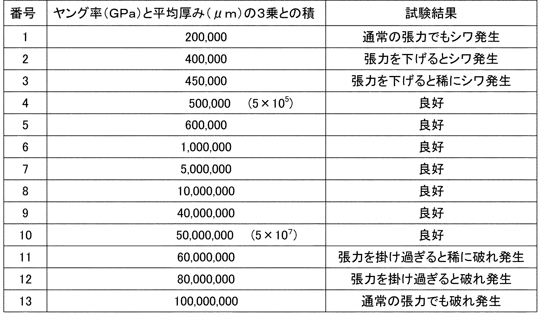
- the transparent conductive pattern layer is formed as a single layer, and the Young's modulus (GPa) and average thickness of the transparent conductor when a tensile test is performed with a load applied in a standard state.
- the transparent conductor is characterized in that the product of ( ⁇ m) and the third power is 5 ⁇ 10 ⁇ 5 to 5 ⁇ 10 ⁇ 7 (GPa ⁇ ⁇ m ⁇ 3).
- the transparent conductor wherein the substrate is a base film that has been stretched in an oblique direction.
- a hydrogenated ring-opening metathesis polymer having a ring structure in which the substrate is connected to the substituents R ⁇ 1 and R ⁇ 2 of the formula (1) is mainly used. It is a transparent conductor characterized by using as a component.
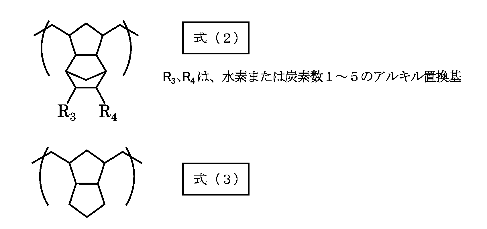
- the hydrogenated ring-opening metathesis polymer is a hydrogenated ring-opening metathesis polymer of the formula (2) in order to obtain transparency and heat resistance of a glass transition temperature of 100 ° C. to 160 ° C. And a copolymer of the hydrogenated ring-opening metathesis polymer of the formula (3) and a transparent conductor.
- the alkyl substituents R ⁇ 3, R of the hydrogenated ring-opening metathesis polymer of the formula (2) are used.
- ⁇ 4 is a transparent conductor characterized in that both are made of hydrogen and the copolymerization ratio with the hydrogenated ring-opening metathesis polymer of the formula (3) is a weight ratio of 40:60 to 99: 1.
- the transparent conductive pattern layer is formed of an amorphous or low-crystal metal oxide, and crystallization of the metal oxide is promoted by far infrared rays. It is a conductor.
- the transparent conductive pattern layer is formed by forming a transparent conductive film containing ultrafine conductor fibers, or by patterning or self-organizing a conductor metal into a fine line, thereby making the appearance transparent. It is a transparent conductor characterized by comprising either a transparent conductive film made visible or a transparent conductive film made of organic matter.
- a routing circuit layer electrically connected to the transparent conductive pattern layer is formed on the substrate, the routing circuit layer is formed of a conductive metal, and the routing circuit layer A part of the routing circuit is exposed to the outside air, and the portion of the routing circuit that is exposed to the outside air serves as a connection terminal for mounting the integrated circuit chip or connecting to an external circuit.
- a routing circuit layer electrically connected to the transparent conductive pattern layer is formed on the substrate, the routing circuit layer is formed of a conductive metal, and the routing circuit layer A part of the routing circuit is exposed to the outside air, and the portion exposed to the outside air of the routing circuit is a connection terminal for mounting the integrated circuit chip or connecting to an external circuit, and the connection terminal remains exposed.
- An eleventh embodiment of the present invention is a substrate used for the transparent conductor described above, comprising a transparent layer and a decorative layer formed in parallel with the transparent layer, the transparent layer and the decorative material The substrate is characterized in that the level difference from the layer is 0 to 2 ⁇ m, and at least one surface of the substrate is flush.
- a twelfth embodiment of the present invention is a substrate used for the transparent conductor described above, wherein the substrate comprises a transparent layer and a decorative layer formed in parallel with the transparent layer, and at least one of the substrates is used. One surface of the substrate is formed by covering the decorative layer with the transparent layer, and at least one surface of the substrate is flush with the substrate.
- a thirteenth embodiment of the present invention is a substrate characterized in that there are no decorative layers in the three outer peripheral directions of the transparent layer, and the entire surface excluding the remaining one-direction decorative layer is a transparent layer.
- the fourteenth embodiment of the present invention is a composite transparent conductor in which a plurality of the transparent conductors are laminated, and has a film thickness of 160 to 400 ⁇ m.
- the fifteenth embodiment of the present invention is a composite transparent conductor in which a plurality of transparent conductors are laminated via an optical adhesive layer or an optical adhesive layer.
- a transparent conductive pattern layer is patterned by a photolithography method and an etching method on a substrate mainly composed of any resin of acrylic, urethane, olefin, polycarbonate, polyester, and polyvinyl chloride.
- the increase in the resistance value of the conductive pattern layer is 20% or less when the transparent conductive pattern layer is formed and extends along a cylinder having a radius of curvature of 20 mm with the transparent conductive pattern layer as an outer surface. Therefore, there is an effect that a transparent conductor on which a very high-definition transparent conductive pattern layer is formed can be obtained. There is also an effect that it can be attached to a curved surface.
- the transparent conductive pattern layer is formed as a single layer, and a Young's modulus (GPa) of the transparent conductor when a tensile test is performed by applying a load at a temperature of 25 ° C. ) And the cube of thickness ( ⁇ m) is 5 ⁇ 10 ⁇ 4 to 5 ⁇ 10 ⁇ 6 (GPa ⁇ ⁇ m ⁇ 3). Therefore, even if a little excessive tension is applied to the transparent conductor, it is difficult to break, and even if the tension is somewhat weak, wrinkles are not easily generated, so that it is very easy to handle and process. Therefore, there is an effect that the transparent conductor can be produced with higher productivity than when the polyimide film is used.
- GPa Young's modulus
- the transparent conductor of the present invention is characterized in that the substrate is a base film stretched in an oblique direction. Therefore, the variation in the orientation angle of the base film is reduced, and there is an effect that a long retardation film having optical anisotropy can be obtained.
- the transparent conductor of the present invention is a hydrogenated ring-opening metathesis polymer having a ring structure in which the substrate is connected to the substituents R ⁇ 1 and R ⁇ 2 of formula (1) in order to obtain transparency and heat resistance. It is characterized by having a main component.
- the hydrogenated ring-opening metathesis polymer of the transparent conductor of the present invention has a hydrogenated ring-opening metathesis weight of formula (2). It consists of a copolymer and a copolymer of the hydrogenated ring-opening metathesis polymer of formula (3).
- the transparent conductor of the present invention has an alkyl substituent R ⁇ 3 of the hydrogenated ring-opening metathesis polymer of the formula (2) in order to obtain transparency and heat resistance of a glass transition temperature of 120 ° C. to 155 ° C.
- Both R ⁇ 4 are composed of hydrogen
- the copolymerization ratio with the hydrogenated ring-opening metathesis polymer of the formula (3) is a weight ratio of 40:60 to 99: 1. Accordingly, not only the conductive pattern layer but also the substrate is a colorless and transparent layer having excellent optical characteristics, and can be applied to a base film or a cover film of a display for displaying an authentication result. The display-related parts can be reduced.
- the transparent conductor of the present invention is characterized in that the transparent conductive pattern layer is formed of an amorphous or low-crystal metal oxide, and crystallization of the metal oxide is promoted by far infrared rays. . Further, the transparent conductor of the present invention is transparent in appearance by forming the transparent conductive pattern layer into a transparent conductive film containing ultrafine conductor fibers, or by patterning or self-organizing a conductor metal into a thin line. It is comprised from either the transparent conductive film made visible, or the transparent conductive film which consists of organic substance. Therefore, the transparent conductive pattern layer is less susceptible to cracking than a transparent conductor composed of a metal oxide that is completely crystallized, and the transparent conductor can be produced with good productivity.
- a routing circuit layer electrically connected to the transparent conductive pattern layer is formed on the substrate, the routing circuit layer is formed of a conductive metal, and the routing circuit is formed.
- a portion of the routing circuit that is exposed to the outside air is a connection terminal for mounting an integrated circuit chip or connecting to an external circuit, and the exposed circuit remains exposed
- the connection terminal is covered with a protective sheet that can be easily detached. Therefore, even if the connection terminal for outputting the authentication result to the outside has a configuration in which the conductor metal is exposed, there is an effect that a problem that connection failure occurs due to rust or corrosion does not occur.
- a routing circuit layer electrically connected to the transparent conductive pattern layer is formed on the substrate, the routing circuit layer is formed of a conductive metal, and the routing circuit is formed.
- the part exposed to the outside air is a connection terminal for mounting an integrated circuit chip or connecting to an external circuit, and the connection terminal is exposed. It is characterized by comprising a structure placed in an atmosphere with a relative humidity of 2 to 70%. Therefore, even if the connection terminal for outputting the authentication result to the outside has a configuration in which the conductor metal is exposed, there is an effect that a problem that connection failure occurs due to rust or corrosion does not occur.
- the substrate of the present invention is a substrate used for the transparent conductor described above, and includes a transparent layer and a decorative layer formed in parallel with the transparent layer.
- the transparent layer and the decorative layer The step is 0 to 2 ⁇ m, and at least one surface of the substrate is flush.
- the substrate of the present invention is a substrate used for the transparent conductor described above, and the substrate comprises a transparent layer and a decorative layer formed in parallel with the transparent layer, and at least one of them.
- the surface is formed by covering the decorative layer with the transparent layer, and at least one of the surfaces of the substrate is flush.
- the substrate of the present invention is characterized in that there are no decorative layers in the three directions of the outer periphery of the transparent layer, and the entire surface excluding the decorative layer in the remaining one direction is a transparent layer. Therefore, there is an effect that the display screen displaying the authentication result due to the provision of the decoration layer is less reduced, and a transparent conductor having a relatively large display screen can be obtained.
- the composite transparent conductor of the present invention is a composite transparent conductor in which a plurality of transparent conductors are laminated and has a film thickness of 160 to 400 ⁇ m. Therefore, since a plurality of transparent conductors are laminated, a plurality of transparent conductive pattern layers for detecting signals are also laminated, which has an effect of improving the accuracy of signal detection. Further, since the thickness is set within an appropriate range, lamination is easy. Therefore, there is an effect that a high performance composite transparent conductor can be manufactured with high productivity.
- the composite transparent conductor of the present invention is a composite transparent conductor in which a plurality of transparent conductors are laminated via an optical adhesive layer or an optical adhesive layer. Therefore, the composite transparent conductor excellent in transparency and adhesiveness can be produced with good productivity.
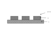
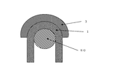
- FIG. 1 is a transparent conductor according to the second embodiment of the present invention
- FIG. 2 is a transparent conductor according to the third embodiment of the present invention
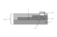
- FIG. 3 is a transparent conductor according to the ninth embodiment of the present invention
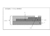
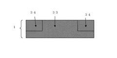
- FIG. 5 shows the substrate of the eleventh embodiment of the present invention
- FIG. 6 shows the substrate of the twelfth embodiment of the present invention
- FIG. 7 shows the substrate of the thirteenth embodiment of the present invention
- FIG. 8 are cross-sectional views each showing an example of the composite transparent conductor according to the fourteenth embodiment of the present invention.
- FIG. 9 is a tensile tester used in the tensile test
- FIG. 10 is a cross-sectional view showing a portion for fixing the test piece of the tensile tester in the tensile test.
- the transparent conductor 100 of the present invention has a structure in which a single transparent conductive pattern layer 3 is formed on a substrate 1 by a photolithography method and an etching method.
- the rise of the resistance value of the conductive pattern layer 3 when the pattern layer 3 is an outer surface and along a cylinder with a curvature radius of 20 mm is within 20%, and a tensile test is performed by applying a load at a temperature of 25 ° C.
- the product of the Young's modulus (GPa) and the cube of the average thickness ( ⁇ m) is 5 ⁇ 10 ⁇ 5 to 5 ⁇ 10 ⁇ 7 (GPa ⁇ ⁇ m ⁇ 3). Young's modulus (GPa) is the initial tensile elastic modulus when the tensile test is carried out.
- the shape of the transparent conductor 100 is not particularly limited, but a sheet-like shape that facilitates the tensile test is preferable.
- the tensile test is a test method based on the measurement method of JIS K7127-1989.
- the chuck 11 is fixed with a screw 16 so that the distance between chucks is 5 mm, the movable member 15 is moved downward at a temperature of 25 ° C., and one end of the test piece 10 is pulled at a constant speed of 200 mm / min. It is a test.
- the transparent conductor 100 has the characteristic value of the said range when a tension test is implemented, even if a tension
- disconnects the transparent conductor 100 in the sheet
- the speed at which the test piece 10 was pulled was set to 200 mm / min, because the actual transport speed when the transparent conductor 100 was produced by roll-to-roll was close to that speed, and was set to that speed. In actual production, the product may be transported at a speed slightly higher or lower than this, but even if the setting of the tensile speed is slightly changed, the actual measurement data hardly changes.
- the substrate 1 may be appropriately stretched.
- the stretching method include a roll stretching method, a tenter clip stretching method, and a rolling method. Stretching may be performed in an oblique direction in addition to longitudinal stretching and lateral stretching.
- a method of stretching in an oblique direction both ends of the substrate 1 are gripped, the substrate 1 is transported while the gripping tool (grip jig) is moved, and the transport direction of the substrate 1 is changed in the middle.
- a method of pulling in an oblique direction By stretching in the oblique direction, variations in the orientation angle of the substrate 1 are reduced.
- the material of the substrate 1 is made of a material mainly composed of any resin of acrylic, urethane, olefin, polycarbonate, polyester, and polyvinyl chloride. This is because these resins have high transparency and appropriate elasticity and strength. And it is cheap compared with a polyimide film, and it leads to the cost reduction of the fingerprint authentication sensor etc. which are final products. Of these, olefin resins made of hydrogenated ring-opening metathesis polymers and polyester resins such as polyethylene terephthalate and polybutylene terephthalate are preferable.
- the method for manufacturing the substrate 1 is not particularly limited, and any method such as injection molding, compression molding, extrusion molding, inflation molding, calendar molding, cast molding, etc. may be used.
- a cyclic polyolefin polymer having a ring structure in which the substituents R ⁇ 1 and R ⁇ 2 in the formula (1) are connected is preferable as the material of the substrate 1.
- Examples of such hydrogenated ring-opening metathesis polymers having a ring structure in which substituents R ⁇ 1 and R ⁇ 2 are connected include hydrogenated ring-opening metathesis polymers of formula (2) and hydrogenation of formula (3). Examples thereof include ring-opening metathesis polymers.
- the weight average molecular weight of these polymers is preferably about 13,000 to 95,000.
- the hydrogenated ring-opening metathesis polymer having a ring structure in which these substituents R ⁇ 1 and R ⁇ 2 are connected is a polymer having a low crystallinity, and is generally a hydrogen in which the substituents R ⁇ 1 and R ⁇ 2 are not connected. It has the feature of high transparency compared to the ring-opening metathesis polymer.
- the glass transition temperature is about 150 to 160 ° C. for the hydrogenated ring-opening metathesis polymer of formula (2), and about 100 ° C. for the hydrogenated ring-opening metathesis polymer of formula (3).
- the transparency is further improved as the number of carbon atoms of the alkyl substituents R ⁇ 3 and R ⁇ 4 is increased, but the glass transition temperature tends to be lowered. Therefore, it is preferable to select an alkyl substituent as appropriate and select a polymer according to the required transparency and heat resistance.
- These polymers for example, use cyclopentadiene as a starting material, and thermally decompose to produce cyclopentadiene, and then produce monomer non-bornenes as intermediates by Diels-Alder method of the cyclopentadiene and olefin.
- the ring-opening metathesis polymer is produced by ring-opening metathesis polymerization of the monomer nonbornenes under a metathesis reaction catalyst, and the double bond of the ring-opening metathesis polymer is hydrogenated using a hydrogenation catalyst. Good.
- the hydrogenated ring-opening metathesis polymer of the formula (2) and the hydrogenated ring-opening metathesis polymer of the formula (3) can also be made into a copolymer. That is, by operating the copolymerization ratio of the copolymer within a weight ratio of 40:60 to 99: 1, a desired transparent and heat-resistant polymer can be obtained over a wider range than the selection of the alkyl substituent. can do.
- a polymer in which the alkyl substituents R ⁇ 3 and R ⁇ 4 of the hydrogenated ring-opening metathesis polymer of formula (2) are both hydrogen is used, and the hydrogenated ring-opening metathesis polymer of formula (2):
- the copolymerization ratio of the hydrogenated ring-opening metathesis polymer of 3) is copolymerized at a weight ratio of 40:60, the glass transition temperature is about 120 ° C., and the copolymerization is performed at a weight ratio of 99: 1.
- the glass transition temperature is about 155 ° C.
- the glass transition temperature is a value measured with a differential scanning calorimeter (DSC-60 manufactured by Shimadzu Corporation) in accordance with JIS K7121.
- Such a substrate 1 is suitable for forming the transparent conductive pattern layer 3 with a very high-definition pattern such as photolithography. It also has excellent resistance to chemicals such as strong acids and strong alkalis. Therefore, the etching solution used for patterning the conductive pattern layer 3 is not deteriorated or discolored, and is suitable as a base material for etching. In addition, since there are no polar groups in the polymer, it has excellent waterproof and moistureproof properties, and also has the property of blocking the penetration of moisture into the back.
- the substrate 1 comprises a transparent layer 33 and a decorative layer 34 formed in parallel with the transparent layer 33, and the step between the transparent layer 33 and the decorative layer 34 is 0 to 2 ⁇ m, and at least the Any one surface of the substrate 1 may be flush (FIG. 5).
- the substrate 1 includes a transparent layer 33 and a decorative layer 34 formed in parallel with the transparent layer 33, and at least one surface of the substrate 1 is covered with the transparent layer 33. It may be formed so that at least one surface of the substrate 1 is flush (FIG. 6).
- the transparent conductive pattern 3 with a very thin film is used. It can be formed without any problems. Therefore, it is possible to manufacture a transparent conductor 100 such as an authentication sensor excellent in design and electrical characteristics.
- the decorative layer 34 is a pattern layer having a thickness of 5 to 200 ⁇ m and is thick. Therefore, the decorative layer 34 has a high concealing property without providing a metal film layer as in Patent Document 1, and is inferior in the concealing property other than black and white. Even if it is a decoration layer which consists of materials etc., there exists the feature which can be applied. Therefore, various colors and patterns can be applied to the decorative layer, and the transparent conductor 100 can have a beautiful appearance with excellent design.
- Examples of the decorative layer 34 include a vinyl resin, a polyamide resin, a polyester resin, an acrylic resin, a polyurethane resin, a polyvinyl acetal resin, an alkyd resin, and the like, and a suitable color pigment or dye. Is formed on a base sheet having releasability by a normal printing method such as screen printing, offset printing, gravure printing, flexographic printing, or mask coating. Alternatively, a sheet containing a colorant may be cut into a predetermined pattern by a method such as punching or laser and laminated on a base sheet having releasability.
- the transparent layer 33 is a layer that is equal to or thicker than the decorative layer 34 and is formed in parallel with the decorative layer 34.
- the step with the decorative layer 34 is 0 to 2 ⁇ m and is transparent. It is a layer whose surface is flush so that the conductive pattern layer 3 and the like can be easily formed. If the level difference with the decorative layer 34 exceeds 2 ⁇ m, variations in thickness and pinholes are likely to occur in the thin transparent conductive pattern layer 3 and the like, and the conductivity becomes unstable and non-uniform.
- the material of the transparent layer 33 is preferably a photocurable resin such as a cyanoacrylate resin, a urethane acrylate resin, a silicone resin, or an unsaturated polyester resin having a high solid content in order to ensure thickness.
- a pattern for position detection is formed simultaneously with the decorative layer 34 on the outside of the base sheet having a surface having a peelable surface, and the position detection is performed.
- a method of reading the pattern for use with an optical sensor or the like and setting it so as to be in parallel with the decorative layer 34 and forming the transparent layer 33 by the normal printing method or the like in the same manner as the decorative layer 34 may be mentioned.
- the decorative layer 34 and the transparent layer 33 of the release sheet are used. And a method of pressing the release sheet by moving the elastic pad up and down from the surface opposite to the surface, and a method of pressing the release sheet by moving the elastic roll and the like left and right.
- the pressing pressure varies depending on the material and thickness of the decorative layer 34 and the transparent layer 33, but is preferably set to about 0.4 to 5 MPa.
- the pressing force is weaker than 0.4 MPa, the flush surface of the release sheet is hardly reflected on the surfaces of the decorative layer 34 and the transparent layer 33, and the surface irregularities of the decorative layer 34 and the transparent layer 33 are large. As a result, it may be difficult to form the transparent conductive pattern layer 3 or the like.
- the pressing force is stronger than 5 MPa, the elastic pad and the elastic roll are easily damaged.
- the transparent layer 33 When the transparent layer 33 is formed to be thicker than the decorative layer 34, a release sheet having a flush surface is placed, and the transparent layer 33 is formed on the decorative layer 34 by pressing when the transparent layer 33 is pressed. (FIG. 6). Even if it protrudes, the transparent layer 33 is transparent and cannot be seen, and it is blocked by the decorative layer 34, so that no problem occurs. And since a part of transparent layer 33 fills the unevenness
- Such materials include heat or room temperature curing and photocuring combined acrylic resin, urethane resin, and the like. When heated or left at room temperature, part of it is cured to form a tack-free gel, which is almost completely cured by light irradiation after being deformed by pressing to form a tough and hard curable film.
- position detection is not necessary, but it is formed by various coaters such as a direct coater method, a lip coater method, a reverse coater method, etc. that can increase the thickness, or by a method such as painting. Is preferred.
- the base sheet having releasability and the release sheet having the same surface are preferably composed of various plastic sheets such as polyester, polyolefin, and polyvinyl chloride.
- the thickness is preferably about 0.01 to 1 mm.
- the surface of the base sheet 1 or the release sheet 11 having releasability may be coated with a resin such as silicon, melamine, or fluorine. In that case, the coated outermost surface must be flush.
- the three-dimensional average surface roughness SRa means the average roughness in the center plane (reference plane) when the surface roughness curve is approximated by a sine curve, and each point obtained with a stylus type three-dimensional surface roughness meter It is a value obtained by measuring the height, taking these measured values into a three-dimensional surface roughness analyzer, and analyzing them, and is a numerical value based on JISB0601-1982.
- the measurement length is 3 mm in the horizontal direction (TD direction) and 5 times at a pitch of 10 ⁇ m in the vertical direction (MD direction). It is the average of the values measured and three-dimensionally analyzed.
- the radius of the tip of the stylus is 2.0 ⁇ m, and a diamond needle with an apex angle of 60 ° is used, and measurement is performed under the conditions of a measuring force of 80 ⁇ N and a cutoff of 0.6 mm.
- the decorative layer 34 and the transparent layer 33 After forming the decorative layer 34 and the transparent layer 33, the decorative layer 34 and the transparent layer 33 reflecting the flush surface of the release sheet by peeling the base sheet and the release sheet having releasability.
- the transparent conductor 10 consisting of is obtained.
- the substrate 1 of the present invention may be configured such that the decorative layer does not exist in the three outer peripheral directions of the transparent layer, and the entire surface excluding the remaining one-direction decorative layer is a transparent layer (FIG. 7). Therefore, there is an effect that the display screen displaying the authentication result due to the provision of the decoration layer is less reduced, and a transparent conductor having a relatively large display screen can be obtained.
- the transparent conductive pattern layer 3 is an electrode layer that performs a sensing function for detecting an electrical signal.
- the transparent conductive pattern layer 3 routes the electrical signal detected by sensing to an integrated circuit chip for control or an external control circuit through a circuit 40. It may be transmitted.
- the material of the transparent conductive pattern layer 3 is made of a transparent conductive film made of a metal oxide, a transparent conductive film containing ultrafine conductor fibers, a transparent conductive film made of fine lines that cannot be visually confirmed, or an organic substance. Examples include a transparent conductive film and a transparent conductive film.
- the transparent conductive pattern layer 3 requires a minimum flexibility.
- the degree of flexibility is a range in which an increase in resistance value does not cause a problem in a test when the transparent conductive pattern layer 3 is placed on the outer surface and along a cylinder having a curvature radius of 20 mm as shown in FIG. It is within 20%.
- the number of times along the test as shown in FIG. 11 is one.
- the transparent conductive film made of metal oxide examples include a transparent conductive film made of tin oxide, indium oxide, antimony oxide, zinc oxide, cadmium oxide, indium tin oxide (ITO), or the like.
- the film forming method include various sputtering methods such as a DC magnetron sputtering method, an RF sputtering method, and a pulse sputtering method, as well as a vacuum deposition method, an ion plating method, and a plating method.
- it may be formed by dissolving or dispersing in a solvent to form a liquid state, spraying or dip coating, and then dispersing the solvent.
- the thickness is preferably about 10 to 800 nm.
- the transparent conductive film containing ultrafine conductor fibers include metal nanowires made of copper, platinum, gold, silver, nickel, etc., silicon nanowires, and transparent conductive films containing carbon nanotubes.
- the diameter of the conductor wire of the ultrafine wire is preferably 0.3 to 100 nm, and the length is preferably about 1 to 100 ⁇ m.
- the two-dimensional network is formed by being dispersed and connected in a binder. Conductivity is exhibited by being formed on the formed film.
- Examples of transparent conductive films consisting of fine lines that cannot be visually confirmed include conductive metals such as silver, copper, palladium, etc., with a line width of about 0.5 to 7 ⁇ m and an aperture ratio (ratio at which no conductive metal pattern is formed per unit area) And 90 to 99% of a transparent conductive film patterned in a lattice shape or a honeycomb shape.
- Examples of the film forming method include an electrolytic or electroless plating method, a vacuum deposition method, a diffusion transfer method, and the like. The thickness is preferably about 0.5 to 30 ⁇ m. *
- the transparent conductive film made of an organic material examples include a thiophene-based conductive polymer such as PEDOT (polyethylenedioxythiophene), a transparent conductive film made of graphene, and the like.
- Examples of the method for forming a transparent conductive film composed of a thiophene-based conductive polymer include the above-mentioned general-purpose printing, painting, and various coating methods, and the thickness is preferably about 1 to 30 ⁇ m.
- a method for forming a transparent conductive film made of graphene it is preferable to form a thin film having a thickness of 0.5 to 100 nm by a CVD method or a plasma CVD method.
- a transparent conductive film made of a metal oxide it is usual to form a pattern on a crystallized metal oxide layer, but such a crystallized metal oxide layer is formed by an etching method. Since it is difficult to remove and difficult to obtain a high-definition pattern, it is not suitable for applications that require a high-definition pattern. On the other hand, if the amorphous or low-crystalline metal oxide layer is left as it is, the resistance value is high, and the sensing accuracy and sensitivity of sensing may be weakened.
- a transparent conductive film is first formed of an amorphous or low crystal metal oxide, and after the patterning of the transparent conductive pattern layer 3, crystallization of the metal oxide is promoted by irradiation with far infrared rays or plasma. Is preferable.
- the transparent conductive pattern layer 3 is made of a non-crystalline or low-crystalline metal oxide that is easy to etch during pattern formation, and thus the transparent conductive pattern layer 3 produces a transparent conductor 100 having a high-definition pattern. Can be manufactured with good performance.
- the electroconductivity of a transparent electrode improves by crystallization and it becomes the transparent conductor 100 with a good touch sensitivity.
- amorphous or low crystal is not limited to a completely amorphous material but also includes a material having a small amount of crystal components. Therefore, in the present invention, the X-ray analysis profile is taken, and a clear X-ray analysis intensity peak indicating crystallization is not observed, but even if a slight peak is observed, the transparent conductive
- the transparent conductor 100 on which the pattern layer 3 is formed is immersed in hydrochloric acid having a concentration of 5% by weight for 15 minutes, then washed and dried, and the resistance between terminals is 10 times or more when the resistance between terminals between 15 mm and 2 is measured. Is defined as “amorphous or low crystalline”. This is because if the metal oxide film is sufficiently crystallized, the film is hardly attacked even by immersion in hydrochloric acid under the above conditions, and the resistance between terminals does not increase so much.
- a photolithography method is used because high-definition patterning is required. That is, a method in which a photoresist layer 70 is applied on the entire surface of the transparent conductive film 21, and a portion to be patterned is exposed and cured, and an uncured portion is removed and patterned (FIGS. 2A to 2D). Or, conversely, the portion to be removed is exposed and softened, and the softened portion of the photoresist layer 70 is removed.
- the transparent conductive film 21 where the photoresist layer 70 is not placed is removed by etching, and the photoresist layer 70 is peeled and removed to form a transparent conductive pattern layer 3 Is formed (FIGS. 2E to 2F).
- Examples of the material of the photoresist layer 70 include vinyl, acrylic, urethane, alkyd, epoxy, polyester, and cellulose resins, and the thickness is preferably about 1 to 50 ⁇ m.
- the method for forming the photoresist layer 70 may be a normal printing method such as screen printing, offset printing, gravure printing, flexographic printing, or a coating method with various coaters.
- Examples of the etching solution for etching the transparent conductive film include ferric chloride aqueous solutions, strong acidic aqueous solutions such as high concentration hydrochloric acid, nitric acid, and sulfuric acid, and strong alkaline aqueous solutions such as caustic soda and caustic potash.
- the routing circuit 40 is generally electrically connected to the transparent conductive pattern layer 3, and a part of the routing circuit 40 is a connection terminal 45 exposed to the outside air.
- An electrical signal detected by the transparent conductive pattern layer 3 is transmitted to an integrated circuit chip or an external circuit smoothly at high speed.
- the routing circuit 40 is preferably made of a conductive metal such as gold, silver, copper, aluminum, nickel, palladium, and the like.
- the routing circuit 40 It is preferable that the integrated circuit chip is directly mounted on the connection terminal 45 in a state where the conductor metal is exposed to the outside as it is or connected to an external circuit.
- connection terminal 45 it is preferable to cover the connection terminal 45 with a protective sheet 46 that can be easily detached (FIG. 3).
- the protective sheet 46 that is easy to desorb it has a water vapor barrier property with a water vapor permeability of 5 g / m 2 or less in an atmosphere of a temperature of 40 ° C. and a relative humidity of 90%, and is specified in JIS-K-6854. In the 180 degree peel test method, a temporary adhesive property of 10 to 500 g weight per 25 mm width at a peel speed of 20 mm / second is preferable.
- the conductor metal of the connection terminal 45 may be passivated (passivation process).
- a method may be employed in which the connection terminals are left exposed in an atmosphere with a relative humidity of 2 to 70% (FIG. 4).
- the method include a method in which the transparent conductor 100 is placed in a container or room capable of maintaining an atmosphere having a predetermined temperature and relative humidity, and a method in which the transparent conductor 100 is sealed and vacuum packaged.
- the relative humidity is a partial pressure of the water vapor pressure with respect to the saturated water vapor pressure
- the saturated water vapor pressure is a value of a saturated water vapor pressure table described in JIS28806.
- the vacuum packaging method since moisture is removed at the time of packaging, there is little fear of rusting in a short period of time.
- a packaging material having a water vapor barrier property in which the water vapor permeability for 24 hours in a% atmosphere is within 20 g / m 2 .
- an inert gas such as nitrogen gas in advance because it prevents intrusion of moisture from the outside air.
- the material of the routing circuit layer 40 includes a case where it is made of a single metal such as copper, aluminum, palladium, nickel, gold, silver, or a case where the metal particles are made of a mixture mixed with a resin binder.
- patterning in the case of the former material there is a method in which a resist is formed on the surface as described above, the resist is patterned by a photolithography method, and a single metal film at a portion where the resist is peeled is removed by etching. Can be mentioned.
- a patterning method for the latter material in addition to this method, a resin binder is used as a photosensitive resin material, and a circuit layer is once formed on the entire surface. Then, an unnecessary portion of the circuit layer is drawn by a photolithography method. The method of removing and patterning is mentioned. This method is more efficient and economical because the above-described resist forming step and etching step are unnecessary.
- the composite transparent conductor 200 of the present invention is a composite transparent conductor in which a plurality of transparent conductors 100 are laminated, and has a film thickness of 160 to 400 ⁇ m. Therefore, since a plurality of transparent conductors 100 are stacked, a plurality of transparent conductive pattern layers 3 for detecting signals are also stacked, so that the accuracy of signal detection is improved. Further, since the thickness is set within an appropriate range, lamination is easy. Therefore, there is an effect that the high-performance composite transparent conductor 200 can be manufactured with high productivity.
- the composite transparent conductor 200 of the present invention is a composite transparent conductor in which a plurality of transparent conductors 100 are laminated via an adhesive base 30. Therefore, the composite transparent conductor 200 excellent in transparency and adhesiveness can be produced with good productivity.
- the adhesive substrate 30 include an optical transparent adhesive tape and an optical curable adhesive layer.
- An optical transparent adhesive tape is a tape in which an adhesive layer made of an acrylic, urethane, or silicone resin is formed on both sides of a separator, and the adhesive layer is scattered from the adhesive solvent or irradiated with ultraviolet rays. As a result, the transparent conductors 100 are firmly bonded to each other.
- the thickness of the adhesive substrate 30 is preferably about 50 to 200 ⁇ m.
Landscapes
- Engineering & Computer Science (AREA)
- General Engineering & Computer Science (AREA)
- Theoretical Computer Science (AREA)
- Human Computer Interaction (AREA)
- Physics & Mathematics (AREA)
- General Physics & Mathematics (AREA)
- Laminated Bodies (AREA)
- Non-Insulated Conductors (AREA)
Abstract
本発明は、透明な導電性パターン層がフォトリソグラフィー法およびエッチング法によりパターン形成されたことを特徴とする透明導電体であって、指紋認証センサに使用する場合のほか、心電・筋電などの生体センサ、電気調光シート、電子広告板、透明アンテナ、タッチセンサなどの様々な用途に適用可能な透明導電体を対象とし、アクリル、ウレタン、オレフィン、ポリカーボネート、ポリエステル、ポリ塩化ビニルのいずれかの樹脂を主成分とする基板上に、透明な導電性パターン層がフォトリソグラフィー法およびエッチング法によりパターン形成され、該透明な導電性パターン層を外側面にして曲率半径20mmの円筒に沿わした場合の該導電性パターン層の抵抗値の上昇が20%以内であることを特徴とする透明導電体である。
Description
本発明は、透明な導電性パターン層がフォトリソグラフィー法およびエッチング法によりパターン形成されたことを特徴とする透明導電体であって、指紋認証センサに使用する場合のほか、心電・筋電などの生体センサ、電気調光シート、電子広告板、透明アンテナ、タッチセンサなどの様々な用途に適用可能な透明導電体を対象とする。
近年、透明導電体はタッチセンサの分野で多く使用されるようになってきたが、指紋認証センサなどの他分野においては、まだガラス素材が大半を占めており、フレキシブルなフィルム素材の使用は少ない。その中で特許文献1は指紋センサの発明であり、デュポン社製のポリイミドフィルムKaptonを基板として使用し、ITOなどの透明な導電線が形成された発明である。
しかし、上記ポリイミドフィルムは、フォトリソグラフィー法およびエッチング法により透明な導電性パターン層を形成する場合には、少し張力を掛けると破れやすく、反対に張力が少ないとシワが生じやすいなど、非常に取扱いが困難な問題があった。また、上記ポリイミドフィルムは高価なフィルムであり、最終製品である指紋認証センサなどのコスト高に繋がる問題もあった。さらに、上記ポリイミドフィルムは茶褐色の有色フィルムのため、認証結果などを表示するディスプレイの基材フィルムまたは被覆フィルムに適用できず、表示のためのディスプレイ関連部品を別途準備する必要もあった。本発明は、以上のような従来技術の課題を解決すべく、以下のような透明導電体を提供するものである。
本発明の第1実施態様は、アクリル、ウレタン、オレフィン、ポリカーボネート、ポリエステル、ポリ塩化ビニルのいずれかの樹脂を主成分とする基板上に、透明な導電性パターン層がフォトリソグラフィー法およびエッチング法によりパターン形成され、該透明な導電性パターン層を外側面にして曲率半径20mmの円筒に沿わした場合の該導電性パターン層の抵抗値の上昇が20%以内であることを特徴とする透明導電体である。
本発明の第2実施態様は、前記透明な導電性パターン層が単層で形成され、標準状態で荷重をかけて引張試験を実施したときの該透明導電体のヤング率(GPa)と平均厚み(μm)の3乗との積が、5×10↑5~5×10↑7(GPa・μm↑3)であることを特徴とする透明導電体である。本発明の第3実施態様は、前記基板が、斜め方向に延伸加工がされた基材フィルムであることを特徴とする透明導電体である。
本発明の第4実施態様は、透明性と耐熱性を得るために、基板が式(1)の置換基R↓1とR↓2がつながった環構造の水素化開環メタセシス重合体を主成分とすることを特徴とする透明導電体である。本発明の第5実施態様は、透明性とガラス転移温度100℃~160℃の耐熱性を得るために、前記水素化開環メタセシス重合体が、式(2)の水素化開環メタセシス重合体と式(3)の水素化開環メタセシス重合体との共重合体とからなることを特徴とする透明導電体である。本発明の第6実施態様は、透明性とガラス転移温度120℃~155℃の耐熱性を得るために、前記式(2)の水素化開環メタセシス重合体のアルキル置換基R↓3、R↓4がともに水素からなり、前記(3)式の水素化開環メタセシス重合体との共重合比率が重量比40:60~99:1からなることを特徴とする透明導電体である。
本発明の第7実施態様は、前記透明な導電性パターン層が非結晶または低結晶の金属酸化物により形成され、遠赤外線により該金属酸化物の結晶化が促進されたことを特徴とする透明導電体である。本発明の第8実施態様は、前記透明な導電性パターン層が、極細線の導体繊維を含有させた透明導電膜、導体金属を細線にパターン化または自己組織化して形成させて外観上透明に見えるようにした透明導電膜、有機物からなる透明導電膜のいずれかから構成されることを特徴とする透明導電体である。
本発明の第9実施態様は、前記基板上に前記透明な導電性パターン層と電気的に接続がされた引き回し回路層が形成され、該引き回し回路層が導体金属から形成され、該引き回し回路の一部が外気に露出した状態で構成され、該引き回し回路の外気に露出した箇所が集積回路チップを実装するか又は外部回路へ接続するための接続端子となっており、該露出したままの接続端子上に脱着が容易な保護シートが被覆されていることを特徴とする透明導電体である。
本発明の第10実施態様は、前記基板上に前記透明な導電性パターン層と電気的に接続がされた引き回し回路層が形成され、該引き回し回路層が導体金属から形成され、該引き回し回路の一部が外気に露出した状態で構成され、該引き回し回路の外気に露出した箇所が集積回路チップを実装するか又は外部回路へ接続するための接続端子となっており、接続端子が露出したままで相対湿度2~70%の雰囲気中に置かれた構成から成ることを特徴とする請求項1ないし請求項8のいずれかに記載の透明導電体である。
本発明の第11実施態様は、前記記載の透明導電体に用いる基板であって、透明層と、該透明層と並列して形成された加飾層とからなり、該透明層と該加飾層との段差が0~2μmであり、少なくとも該基板のいずれか片方の面が面一であることを特徴とする基板である。本発明の第12実施態様は、前記記載の透明導電体に用いる基板であって、前記基板が、透明層と、該透明層と並列して形成された加飾層とからなり、少なくともいずれか片方の面が該加飾層上に該透明層が被覆して形成されており、少なくとも基板のいずれか片方の面が面一であることを特徴とする基板である。本発明の第13実施態様は、前記透明層の外周3方向に加飾層が存在せず、残り1方向の加飾層を除く全面が透明層であることを特徴とする基板である。
本発明の第14実施態様は、前記透明導電体が複数積層された複合透明導電体であって、膜厚が160~400μmである複合透明導電体である。本発明の第15実施態様は、光学接着剤層または光学粘着剤層を介して透明導電体が複数積層された複合透明導電体である。
本発明の透明導電体は、アクリル、ウレタン、オレフィン、ポリカーボネート、ポリエステル、ポリ塩化ビニルのいずれかの樹脂を主成分とする基板上に、透明な導電性パターン層がフォトリソグラフィー法およびエッチング法によりパターン形成され、該透明な導電性パターン層を外側面にして曲率半径20mmの円筒に沿わした場合の該導電性パターン層の抵抗値の上昇が20%以内であることを特徴とする。したがって、非常に高精細な透明な導電性パターン層を形成した透明導電体を得ることができる効果がある。また、曲面の箇所に装着できる効果もある。
また、本発明の透明導電体は、前記透明な導電性パターン層が単層で形成され、25℃の温度下で荷重をかけて引張試験を実施したときの該透明導電体のヤング率(GPa)と厚み(μm)の3乗との積が、5×10↑4~5×10↑6(GPa・μm↑3)であることを特徴とする。したがって、該透明導電体に少々過度の張力を掛けても破れにくく、また張力が多少弱くともシワが生じにくいため、非常に取扱いやすく、加工がし易い。従って、ポリイミドフィルムを用いる場合よりも透明導電体を生産性良く製造できる効果がある。また、本発明の透明導電体は、前記基板が、斜め方向に延伸加工がされた基材フィルムであることを特徴とする。したがって、基材フィルムの配向角のバラつきが低減され、光学異方性を有する長尺の位相差フィルムにすることができる効果がある。
また、本発明の透明導電体は、透明性と耐熱性を得るために、基板が式(1)の置換基R↓1とR↓2がつながった環構造の水素化開環メタセシス重合体を主成分とすることを特徴とする。また、本発明の透明導電体は、透明性とガラス転移温度100℃~160℃の耐熱性を得るために、前記水素化開環メタセシス重合体が、式(2)の水素化開環メタセシス重合体と式(3)の水素化開環メタセシス重合体との共重合体とからなることを特徴とする。また、本発明の透明導電体は、透明性とガラス転移温度120℃~155℃の耐熱性を得るために、前記式(2)の水素化開環メタセシス重合体のアルキル置換基R↓3、R↓4がともに水素からなり、前記(3)式の水素化開環メタセシス重合体との共重合比率が重量比40:60~99:1からなることを特徴とする。したがって、導電性パターン層のみならず、基板も無色透明な光学特性に優れた層となり、認証結果などを表示するディスプレイの基材フィルムまたは被覆フィルムに適用することが可能なため、該表示のためのディスプレイ関連部品を削減することができる効果がある。
また、本発明の透明導電体は、前記透明な導電性パターン層が非結晶または低結晶の金属酸化物により形成され、遠赤外線により該金属酸化物の結晶化が促進されたことを特徴とする。また、本発明の透明導電体は、前記透明な導電性パターン層が、極細線の導体繊維を含有させた透明導電膜、導体金属を細線にパターン化または自己組織化して形成させて外観上透明に見えるようにした透明導電膜、有機物からなる透明導電膜のいずれかから構成されることを特徴とする。したがって、透明な導電性パターン層が完全に結晶化した金属酸化物から構成される透明導電体よりもクラックが入りにくく、透明導電体を生産性良く製造できる効果がある。
また、本発明の透明導電体は、前記基板上に前記透明な導電性パターン層と電気的に接続がされた引き回し回路層が形成され、該引き回し回路層が導体金属から形成され、該引き回し回路の一部が外気に露出した状態で構成され、該引き回し回路の外気に露出した箇所が集積回路チップを実装するか又は外部回路へ接続するための接続端子となっており、該露出したままの接続端子上に脱着が容易な保護シートが被覆されていることを特徴とする。したがって、認証結果を外部に出力するなどのための接続端子が、導体金属が露出したままの構成であったとしても錆たり腐食して接続不良となる不具合は発生しないという効果がある。
また、本発明の透明導電体は、前記基板上に前記透明な導電性パターン層と電気的に接続がされた引き回し回路層が形成され、該引き回し回路層が導体金属から形成され、該引き回し回路の一部が外気に露出した状態で構成され、該引き回し回路の外気に露出した箇所が集積回路チップを実装するか又は外部回路へ接続するための接続端子となっており、接続端子が露出したままで相対湿度2~70%の雰囲気中に置かれた構成から成ることを特徴とする。したがって、認証結果を外部に出力するなどのための接続端子が、導体金属が露出したままの構成であったとしても錆たり腐食して接続不良となる不具合は発生しないという効果がある。
また、本発明の基板は、前記記載の透明導電体に用いる基板であって、透明層と、該透明層と並列して形成された加飾層とからなり、該透明層と該加飾層との段差が0~2μmであり、少なくとも該基板のいずれか片方の面が面一であることを特徴とする。また、本発明の基板は、前記記載の透明導電体に用いる基板であって、前記基板が、透明層と、該透明層と並列して形成された加飾層とからなり、少なくともいずれか片方の面が該加飾層上に該透明層が被覆して形成されており、少なくとも基板のいずれか片方の面が面一であることを特徴とする。
したがって、透明導電体に加飾層を設けたい場合にも、基板に加飾層を設けたことによる段差や凹凸の発生がほとんど無いため、非常に薄膜の透明な導電パターンであっても問題なく形成できる。意匠性および電気特性に優れた認証センサなどの透明導電体を製造できる効果がある。
また、本発明の基板は、前記透明層の外周3方向に加飾層が存在せず、残り1方向の加飾層を除く全面が透明層であることを特徴とする。したがって、加飾層を設けたことによる認証結果を表示する表示画面の縮小が少なく、相対的に表示画面の大きい透明導電体にすることができる効果がある。
また、本発明の複合透明導電体は、記透明導電体が複数積層された複合透明導電体であって、膜厚が160~400μmである。したがって、透明導電体が複数積層されたため、信号を検出する透明な導電性パターン層も複数積層されるため、信号検出の精度が向上する効果がある。また、厚みも適度な範囲内に設定されるため積層もし易い。したがって、高性能の複合透明導電体を生産性良く製造できる効果がある。
また、本発明の複合透明導電体は、光学接着剤層または光学粘着剤層を介して透明導電体が複数積層された複合透明導電体である。したがって、透明性および接着性に優れた複合透明導電体を生産性良く製造できる効果がある。
本発明の好ましい実施形態を、図面を参照して詳述する。図1は本発明の第2実施態様の透明導電体、図2は本発明の第3実施態様の透明導電体、図3は本発明の第9実施態様の透明導電体、図4は本発明の第10実施態様の透明導電体、図5は本発明の第11実施態様の基板、図6は本発明の第12実施態様の基板、図7は本発明の第13実施態様の基板、図8は本発明の第14実施態様の複合透明導電体の、各々一例を示す断面図である。しかし、本発明はこれらの一例に限定されるものではない。また、図9は引張試験において使用する引張試験機、図10は引張試験において引張試験機の試験片を固定する部分を示す断面図である
本発明の透明導電体100は、図1に示すように基板1上に単層の透明な導電性パターン層3がフォトリソグラフィー法およびエッチング法により形成された構成であって、該透明な導電性パターン層3を外側面にして曲率半径20mmの円筒に沿わした場合の該導電性パターン層3の抵抗値の上昇が20%以内であり、25℃の温度下で荷重をかけて引張試験を実施したときのヤング率(GPa)と平均厚み(μm)の3乗との積が、5×10↑5~5×10↑7(GPa・μm↑3)である特徴を有する。ヤング率(GPa)は上記引張試験を実施したときの初期引張弾性率である。透明導電体100の形状は、とくに限定されるわけではないが、引張試験を実施しやすいシート状の形状が好ましい。
引張試験は、JIS K7127-1989の測定方法に基づいた試験法であって、図9に示すような引張試験機に、図10に示すように幅10mmの透明導電体100の試験片10を一対のチャック11を用いてチャック間距離が5mmになるようねじ16で固定し、25℃の温度下において可動部材15を下部に移動させて、試験片10の一端を200mm/分の一定速度で引っ張る試験である。そして、引張試験を実施したときに透明導電体100が上記範囲の特性値を有していると、破れにくく、また張力が多少弱くともシワが生じにくい(下記の表1参照)。そして、適度の弾力性を有するため、取扱いもし易い。
なお、試験片10は、透明導電体100を幅10mm、チャック間距離5mmで引張試験に供することができるサイズのシート形状に切断したものである。試験片10のサイズを大きくし過ぎると、試験片10の形状のバラツキが生じる。また、試験片10のサイズをあまりに小さくし過ぎると測定誤差が大きくなる。したがって、測定誤差が問題にならない程度にできるだけ小さくした結果、上記のサイズが最も適したサイズとなる。なお、試験片10を引張する速度を200mm/分としたのは、透明導電体100をロールツーロールで生産する際の実際の搬送速度が、その速度に近いため、その速度に設定した。実際の生産時にはこれより多少前後した速度で搬送される場合があるが、引張速度の設定を多少変えても実際の測定データは殆ど変わらないので、これで十分シミュレートできている。
基板1は適宜延伸加工をしてもよい。延伸加工の方法としては、ロール延伸法、テンタークリップ延伸法、圧延法等が挙げられる。延伸は縦延伸・横延伸のほか斜め方向に延伸加工してもよい。斜め方向に延伸加工する方法としては、基板1の両端部を把持(grip)し、把持具(grip jig)を移動させながら基板1を搬送するとともに、基板1の搬送方向を途中で変えることにより、斜め方向に引っ張る方法が挙げられる。該斜め方向に延伸加工することによって、基板1の配向角のバラつきが低減される。
基板1の材質は、アクリル、ウレタン、オレフィン、ポリカーボネート、ポリエステル、ポリ塩化ビニルのいずれかの樹脂を主成分とする材質で構成する。これらの樹脂は、透明性が高く適度な弾力性と強度を有するためである。そして、ポリイミドフィルムに比べて安価であり、最終製品である指紋認証センサなどのコスト低減に繋がるためである。その中でも水素化開環メタセシス重合体からなるオレフィン系樹脂やポリエチレンテレフタレート、ポリブチレンテレフタレートなどのポリエステル系樹脂が好ましい。基板1の製造方法はとくに限定は無く、射出成形、圧縮成形、押出成形、インフレーション成形、カレンダー成形、キャスト成形など、いずれの方式でも構わない。
水素化開環メタセシス重合体からなるオレフィン系樹脂の中でも式(1)の置換基R↓1とR↓2がつながった環構造の環状ポリオレフィン系ポリマーが、基板1の材質として好ましい。そのような置換基R↓1とR↓2がつながった環構造の水素化開環メタセシス重合体の例としては、式(2)の水素化開環メタセシス重合体や式(3)の水素化開環メタセシス重合体などが挙げられる。これらの重合体の重量平均分子量は、13,000~95,000程度が好ましい。
これらの置換基R↓1とR↓2がつながった環構造の水素化開環メタセシス重合体は結晶化度が低いポリマーで、一般的に置換基R↓1とR↓2がつながっていない水素化開環メタセシス重合体に比べて透明性が高いという特長を有する。ガラス転移温度は、式(2)の水素化開環メタセシス重合体で150~160℃くらい、式(3)の水素化開環メタセシス重合体で100℃くらいである。式(2)の水素化開環メタセシス重合体は、アルキル置換基R↓3やR↓4の炭素数が多いほど透明性はさらに向上するが、ガラス転移温度は低下する傾向にある。したがって、アルキル置換基を適宜選択して必要とする透明性および耐熱性等に応じたポリマーを選択するとよい。
これらの重合体は、例えばジシクロペンタジエン類を出発原料に、熱分解してシクロペンタジエン類を生成し、該シクロペンタジエン類とオレフィンとのディールスアルダー法によって中間体であるモノマーノンボルネン類を生成し、該モノマーノンボルネン類をメタセシス反応触媒下で開環メタセシス重合して開環メタセシス重合体を生成し、水素化触媒を用いて該開環メタセシス重合体の二重結合を水素化して生成するとよい。
また、該式(2)の水素化開環メタセシス重合体と式(3)の水素化開環メタセシス重合体とは、共重合体にすることもできる。すなわち、該共重合体の共重合比率を重量比40:60~99:1の範囲内で操作することによって、前記アルキル置換基の選択以上の広範囲に渡る所望の透明性および耐熱性のポリマーにすることができる。
たとえば、式(2)の水素化開環メタセシス重合体のアルキル置換基R↓3、R↓4がともに水素からなる重合体を用い、式(2)の水素化開環メタセシス重合体:式(3)の水素化開環メタセシス重合体の共重合比率が、重量比40:60で共重合した場合には、ガラス転移温度は120℃くらいであり、重量比99:1で共重合した場合には、ガラス転移温度は155℃くらいとなる。なお、前記ガラス転移温度は、JIS K7121に準拠して示差走査熱量測定器(株式会社島津製作所製DSC-60)により測定した値である。
このような基板1は、フォトリソグラフィーのような非常に高精細なパターンで透明な導電性パターン層3を形成するのに適している。また、強酸や強アルカリなどの薬品に対しても優れた耐性を有する。よって、導電性パターン層3をパターン化する際に用いるエッチング液に対して劣化・変色するようなことはなく、エッチングする際の基材としても適している。また、重合体中に極性基がないため、優れた防水性および防湿性を有し、背後への水分の侵入をブロックする性質も有する。
また、基板1は透明層33と該透明層33と並列して形成された加飾層34とからなり、該透明層33と該加飾層34との段差が0~2μmであり、少なくとも該基板1のいずれか片方の面が面一であるようにしてもよい(図5)。また、基板1は透明層33と該透明層33と並列して形成された加飾層34とからなり、少なくともいずれか片方の面が該加飾層34上に該透明層33が被覆して形成されており、少なくとも基板1のいずれか片方の面が面一であるようにしてもよい(図6)。
したがって、透明導電体100に加飾層34を設けたい場合にも、基板1に加飾層34を設けたことによる段差や凹凸の発生がほとんど無いため、非常に薄膜の透明な導電パターン3であっても問題なく形成できる。したがって、意匠性および電気特性に優れた認証センサなどの透明導電体100を製造できる。
また加飾層34は、厚さ5~200μmのパターン層であり、分厚いため、特許文献1のような金属膜層を設けなくても隠蔽性が高く、黒や白以外の隠蔽性に劣る色材等からなる加飾層であっても適用できる特長がある。したがって、加飾層は様々な色・模様を適用でき、透明導電体100を意匠性に優れた美麗な外観とすることができる。
加飾層34の例としては、ビニル系樹脂、ポリアミド系樹脂、ポリエステル系樹脂、アクリル系樹脂、ポリウレタン系樹脂、ポリビニルアセタール系樹脂、アルキド系樹脂などをバインダーとし、適切な色の顔料または染料などを着色剤として含有する着色インキ層が挙げられ、スクリーン印刷、オフセット印刷、グラビア印刷、フレキソ印刷などの通常印刷法やマスク塗装などの方法で離型性を有する基体シート上に形成する。あるいは、着色剤を含有するシートを打ち抜きやレーザーなどの方法により所定のパターンにカットして離型性を有する基体シート上に積層形成してもよい。
透明層33は、加飾層34と同等または加飾層34よりも厚膜で加飾層34と並列して形成する層であり、加飾層34との段差を0~2μmとし、透明な導電性パターン層3等を形成しやすいよう表面を面一とした層である。加飾層34との段差が2μmを越えれば、薄膜の透明な導電性パターン層3等に厚みのバラツキやピンホールが発生しやすくなり、導電性が不安定・不均一となる。なお透明層33の材質は、厚みを確保するために固形分の含有率が高いシアノアクリレート系樹脂、ウレタンアクリレート系樹脂、シリコーン系樹脂、不飽和ポリエステル系樹脂などの光硬化性樹脂等が好ましい。
透明層33を加飾層34と並列して形成する方法としては、表面が面一の剥離性を有する基体シートの場外に位置検知用のパターンを加飾層34と同時に形成し、該位置検知用のパターンを光学センサなどで読み取って、加飾層34と並列する位置になるよう設定し、透明層33を上記加飾層34と同様に通常印刷法などによって形成する方法が挙げられる。
加飾層34および透明層33上に表面が面一の離型シートを載せて加飾層34および透明層33を面一にする方法としては、離型シートの加飾層34および透明層33と反対側の面から、弾性体パッドなど上下させて離型シートを押圧する方法や弾性体ロールなどを左右に移動させて離型シートを押圧する方法などが挙げられる。押圧する圧力は加飾層34および透明層33の材質・厚みによって異なるが、0.4~5MPa程度に設定するとよい。押圧力が0.4MPaより弱いと、離型シートの面一の表面が加飾層34および透明層33の表面に反映されにくくなり、加飾層34および透明層33の表面凹凸が大きい状態のままとなって、透明な導電性パターン層3等の形成が困難となる場合がある。一方、押圧力を5MPaより強くすると、弾性体パッドや弾性体ロールが傷みやすくなる。
透明層33を加飾層34よりも厚膜で形成した場合は、表面が面一の離型シートを載せ、その載せたときの押圧により加飾層34上に透明層33をはみ出して形成してもよい(図6)。はみ出ても透明層33が透明で見えないうえに、加飾層34によって遮られるので、全く問題は生じない。そして、透明層33の一部が加飾層34の凹凸を埋めて均すので、透明層33の形成面は離型シートの面一の表面がそのまま反映されて面一となる。この場合、透明層33の材質は押圧により変形が容易な流動性のある材質であることが必要となる。
そのような材質としては、熱又は常温硬化と光硬化の併用型のアクリル系樹脂、ウレタン樹脂等が挙げられる。加熱または常温放置で一部が硬化しタックフリーのゲル状になり、押圧により変形をさせた後の光照射によりほぼ完全に硬化して強靭で硬い硬化性皮膜が形成される。透明層33を加飾層34上にも形成する場合は、位置検知は必要ないが、厚みを稼げるダイレクトコーター法、リップコーター法、リバースコーター法などの各種コーターや塗装などによる方法によって形成するのが好ましい。
離型性を有する基体シートや表面が面一の離型シートは、ポリエステル、ポリオレフィン、ポリ塩化ビニルなどの各種プラスチックシートなどで構成するとよい。厚みは、0.01~1mm程度が好ましい。離型性を有する基体シート1や離型シート11の表面には離型性をより向上させるために、シリコン、メラミン、フッ素などの樹脂をコートしておいてもよい。その場合には、そのコートされた最表面が面一であることが必要である。
なお、面一とは、これらの表面がほぼフラットな状態のことを指し、三次元平均表面粗さSRaの数値が500nm以下の範囲であることを指す。三次元平均表面粗さSRaは、表面粗さ曲線をサインカーブで近似した際の中心面(基準面)における平均粗さを意味し,触針式三次元表面粗さ計で得た各点の高さを測定し、これらの測定値を三次元表面粗さ解析装置に取り込んで解析することにより得られた値であり、JISB0601-1982に準拠した数値である。具体的には、(株)小坂研究所製の全自動微細形状測定機SURFCORDER ET4000Aを用いて、横方向(TD方向)に測定長さ3mmで、縦方向(MD方向)に10μmピッチで5回測定して3次元解析した値の平均値である。尚、触針先端半径は2.0μmで、頂角60°のダイヤモンド針を使用し、測定力80μN、カットオフ0.6mmの条件で測定する。
加飾層34および透明層33を形成後、離型性を有する基体シート及び離型シートを剥離することにより、離型シートの面一な面が反映された加飾層34と透明層33とからなる透明導電体10が得られる。
また、本発明の基板1は、前記透明層の外周3方向に加飾層が存在せず、残り1方向の加飾層を除く全面が透明層であるようにしてもよい(図7)。したがって、加飾層を設けたことによる認証結果を表示する表示画面の縮小が少なく、相対的に表示画面の大きい透明導電体にすることができる効果がある。
透明な導電性パターン層3は、電気信号を検知するためのセンシング機能を果たす電極層であり、センシングによって検知された電気信号を引き回し回路40を通じて制御用の集積回路チップや外部の制御回路へと伝達されるようにしてもよい。透明な導電性パターン層3の材質としては、金属酸化物からなる透明導電膜、極細線の導体繊維を含有させた透明導電膜、目視で確認できない程度の細線からなる透明導電膜、有機物からなる透明導電膜透明導電膜などが挙げられる。そして、透明な導電性パターン層3は最小限の柔軟性を必要とする。該柔軟性の程度は、透明な導電性パターン層3を外側面にして図11に示したように曲率半径20mmの円筒に沿わした場合の試験で抵抗値の上昇が問題とならない範囲であり、それは20%以内である。なお、該試験で図11のように沿わした回数は1回である。
金属酸化物からなる透明導電膜の例としては、酸化錫、酸化インジウム、酸化アンチモン、酸化亜鉛、酸化カドミウム、インジウムスズ酸化物(ITO)などからなる透明導電膜が挙げられる。製膜方法としては、DCマグネトロンスパッタ法、RFスパッタ法、パルススパッタ法などの種々のスパッタリング法のほか、真空蒸着法、イオンプレーティング法、鍍金法などが挙げられる。また、溶媒に溶解または分散させて液体状態にし、スプレーやディップコーティングした後に溶媒を飛散させて形成する方法でも構わない。厚みは10~800nm程度とするのが好ましい。
極細線の導体繊維を含有させた透明導電膜の例としては、銅、白金、金、銀、ニッケル等からなる金属ナノワイヤやシリコンナノワイヤ、カーボンナノチューブを含有させた透明導電膜が挙げられる。光学特性および電気特性の観点から該極細線の導体繊維の直径は0.3~100nm、長さは1~100μm程度の寸法の導体繊維が好ましく、バインダー中に分散・連結されて二次元ネットワークが形成される膜に形成されることによって導電性が発揮される。
目視で確認できない程度の細線からなる透明導電膜の例としては、銀、銅、パラジウムなどの導体金属を線幅0.5~7μm程度、開口率(単位面積あたりの導体金属パターンが形成されない比率)90~99%の格子状またはハニカム状にパターン化した透明導電膜等が挙げられる。製膜方法としては、電解または無電解のメッキ法のほか、真空蒸着法や拡散転写法などにより形成する方法が挙げられる。厚みは0.5~30μm程度とするのが好ましい。
有機物からなる透明導電膜の例としては、PEDOT(ポリエチレンジオキシチオフェン)などのチオフェン系導電ポリマーやグラフェン等からなる透明導電膜が挙げられる。チオフェン系導電ポリマーからなる透明導電膜の製膜方法としては、前出の汎用印刷や塗装、各種コーターにより形成する方法が挙げられ、厚みは1~30μm程度とするのが好ましい。グラフェンからなる透明導電膜の製膜方法としては、CVD法やプラズマCVD法などによって0.5~100nmの薄膜で形成するのが好ましい。
とくに、金属酸化物からなる透明導電膜では、一般的には結晶化した金属酸化物層に対してパターン形成するのが通常であるが、そのような結晶化した金属酸化物層はエッチング法による除去がしにくく高精細なパターンにしにくいため、高精細なパターンを必要とする用途にはあまり向いていない。一方、非結晶または低結晶の金属酸化物層はそのままの状態では抵抗値が高くてセンシングの検出精度や検出感度が弱くなる場合もある。
したがって、まず非結晶または低結晶の金属酸化物による透明導電膜を形成し、透明な導電性パターン層3のパターン形成後に、遠赤外線またはプラズマの照射により該金属酸化物の結晶化を促進させるようにするのが好ましい。このようにすることにより、パターン形成時はエッチングがしやすい非結晶または低結晶の金属酸化物で構成されるため、透明な導電性パターン層3が高精細なパターンからなる透明導電体100を生産性良く製造できる。そして、パターン形成後は、結晶化により透明電極の導電性が向上しタッチ感度の良い透明導電体100となる。
なお、「非結晶または低結晶」とは、完全に非晶質であるものに限られず少量の結晶成分を有している場合のものも含むことを意味する。したがって本発明では、X線解析のプロファイルを採り、結晶化を示す明確なX線解析強度のピークが見られない場合は勿論のこと、仮に該ピークが少し見られた場合でも、透明な導電性パターン層3が形成された透明導電体100を濃度5重量%の塩酸に15分間浸漬した後、水洗・乾燥し、15mm↑2間の端子間抵抗を測定した場合に端子間抵抗が10倍以上に上昇するような場合は「非結晶または低結晶」と定義する。充分に結晶化された金属酸化物膜であれば上記の条件での塩酸浸漬でも皮膜が侵されることは少なく、端子間抵抗がそのように大幅増大することはないからである。
透明な導電性パターン層3をパターン化する手段は、高精細のパターン化が必要なためフォトリソグラフィーによる方法を用いる。すなわち、フォトレジスト層70を透明導電膜21上の全面に塗布し、パターン化させたい箇所を露光して硬化させ未硬化部分を除去しパターン化する方法(図2(a)~(d))や、その逆の除去したい箇所を露光して軟化させ軟化した部分のフォトレジスト層70を除去する方法である。そして該フォトレジスト層70をパターン化した後は、該フォトレジスト層70の載っていない箇所の透明導電膜21をエッチングにより除去し、フォトレジスト層70を剥離除去して透明な導電性パターン層3が形成される(図2(e)~(f))。
フォトレジスト層70の材質としてはビニル系、アクリル系、ウレタン系、アルキッド系、エポキシ系、ポリエステル系、セルロース系などの樹脂が挙げられ、厚みは1~50μm程度が好ましい。フォトレジスト層70の形成方法は、スクリーン印刷、オフセット印刷、グラビア印刷、フレキソ印刷、などの通常印刷法の他、塗装や各種コーターでのコート法でも構わない。また、上記透明導電膜をエッチングするためのエッチング液としては塩化第二鉄水溶液のほか、高濃度の塩酸、硝酸、硫酸などの強酸性水溶液や苛性ソーダ、苛性カリなどの強アルカリ性水溶液などが挙げられる。
そして、透明な導電性パターン層3には、一般的に引き回し回路40が電気的に接続形成され、引き回し回路40の一部は外気に露出した接続端子45となっており、該接続端子45を通じて透明な導電性パターン層3で検出した電気信号は高速かつ円滑に集積回路チップや外部回路へ伝達される。高速に伝達する目的から、引き回し回路40は高導電性の金、銀、銅、アルミニウム、ニッケル、パラジウムなどの導体金属から構成するのが好ましく、接触抵抗値の上昇を避けるために引き回し回路40の導体金属がそのまま外気に露出した状態の接続端子45に直接集積回路チップを実装したり、外部回路と接続するのが好ましい。
しかし、引き回し回路40の導体金属がそのまま外気に露出した状態であると腐食や錆が発生するので、接続端子45上には脱着が容易な保護シート46を被覆するのが好ましい(図3)。脱着が容易な保護シート46としては、温度40℃、相対湿度90%の雰囲気内での24時間の水蒸気透過度が5g/m2以内の水蒸気バリア性を有し、JIS-K-6854に規定される180度剥離試験法において剥離速度20mm/秒で25mm幅あたり10~500g重の仮接着性を有するものが好ましい。なお、接続端子45の導体金属には不動態化処理(パッシベーション処理)をしてもよい。
あるいは、前記保護シート46を被覆する替わりに、接続端子を露出させたままで相対湿度2~70%の雰囲気中に置いておく方法でも構わない(図4)。該方法としては、透明導電体100を所定の温度および相対湿度の雰囲気を維持できる容器や部屋内に置く方法や、透明導電体100を密閉して真空包装する方法などが挙げられる。なお、ここでいう相対湿度とは飽和水蒸気圧に対する水蒸気圧の分圧のことであり、飽和水蒸気圧は、JIS28806に記載されている飽和水蒸気圧表の値である。真空包装する方法では包装した時点で湿気が除去されるため短期間で錆びる懸念は少ないが、時間経過とともに外気の湿気が包装材を通過して内部に浸透するので、温度40℃、相対湿度90%の雰囲気内での24時間の水蒸気透過度が20g/m2以内の水蒸気バリア性の特性をもつ包装材を使用して包装するのが好ましい。そして、包装した内部には予め窒素ガスなどの不活性なガスを充填させておけば外気の湿気の侵入防止になるのでより好ましい。
引き回し回路層40の材質は、銅、アルミニウム、パラジウム、ニッケル、金、銀などの単体金属から成る場合や、それらの金属粒子が樹脂バインダーに混ざった混合物から成る場合などが挙げられる。前者の材質の場合のパターン化としては、前述のとおりレジストを表面に形成して、レジストをフォトリソグラフィーによる方法でパターン化し、レジストが剥離された箇所の単体金属の膜をエッチングで除去する方法が挙げられる。後者の材質の場合のパターン化としては、該方法の他に、樹脂バインダーを感光性樹脂材料にして引き回し回路層を一旦全面に形成した後、フォトリソグラフィーによる方法で引き回し回路層の不要な箇所を除去してパターン化する方法が挙げられる。この方法では、前述のレジストを形成する工程やエッチング工程が不要になるので、より効率的・経済的である。
また、本発明の複合透明導電体200は、透明導電体100が複数積層された複合透明導電体であって、膜厚が160~400μmである。したがって、透明導電体100が複数積層されたため、信号を検出する透明な導電性パターン層3も複数積層されるため、信号検出の精度が向上する。また、厚みも適度な範囲内に設定されるため積層もし易い。したがって、高性能の複合透明導電体200を生産性良く製造できる効果がある。
また、本発明の複合透明導電体200は、接着基材30を介して透明導電体100が複数積層された複合透明導電体である。したがって、透明性および接着性に優れた複合透明導電体200を生産性良く製造できる効果がある。接着基材30としては、光学用透明粘着テープや光学用硬化型接着剤層が挙げられる。光学用透明粘着テープとは、セパレーターの両面にアクリル系、ウレタン系、シリコーン系等の樹脂からなる粘着剤層が形成されたテープであり、該粘着剤層は粘着剤の溶媒の飛散または紫外線照射により固化して透明導電体100どうしが強固に接着する。接着基材30としての厚みは50~200μm程度が好ましい。
1 基板
3 透明な導電性パターン層
10 試験片
11 チャック
15 可動部材
16 ねじ
21 透明導電膜
30 接着基材
33 透明層
34 加飾層
40 引き回し回路
45 接続端子
46 保護シート
70 フォトレジスト層
80 円筒
100 透明導電体
3 透明な導電性パターン層
10 試験片
11 チャック
15 可動部材
16 ねじ
21 透明導電膜
30 接着基材
33 透明層
34 加飾層
40 引き回し回路
45 接続端子
46 保護シート
70 フォトレジスト層
80 円筒
100 透明導電体
Claims (15)
- アクリル、ウレタン、オレフィン、ポリカーボネート、ポリエステル、ポリ塩化ビニルのいずれかの樹脂を主成分とする基板上に、透明な導電性パターン層がフォトリソグラフィー法およびエッチング法によりパターン形成され、前記透明な導電性パターン層を外側面にして曲率半径20mmの円筒に沿わした場合の前記導電性パターン層の抵抗値の上昇が20%以内である、透明導電体。
- 前記透明な導電性パターン層が単層で形成され、標準状態で荷重をかけて引張試験を実施したときのヤング率(GPa)と平均厚み(μm)の3乗との積が、5×10↑5~5×10↑7(GPa・μm↑3)である、請求項1に記載の透明導電体。
- 前記基板が、斜め方向に延伸加工がされた基材フィルムである、請求項1または請求項2のいずれかに記載の透明導電体。
- 透明性と耐熱性を得るために、基板が式(1)の置換基R↓1とR↓2がつながった環構造の水素化開環メタセシス重合体を主成分とする、請求項1から請求項3のいずれかに記載の透明導電体。

- 透明性とガラス転移温度100℃~160℃の耐熱性を得るために、前記水素化開環メタセシス重合体が、式(2)の水素化開環メタセシス重合体と式(3)の水素化開環メタセシス重合体との共重合体とからなる、請求項4に記載の透明導電体。
- 透明性とガラス転移温度120℃~155℃の耐熱性を得るために、前記式(2)の水素化開環メタセシス重合体のアルキル置換基R↓3、R↓4がともに水素からなり、前記(3)式の水素化開環メタセシス重合体との共重合比率が重量比40:60~99:1からなる、請求項5に記載の透明導電体。
- 前記透明な導電性パターン層が非結晶または低結晶の金属酸化物により形成され、遠赤外線により前記金属酸化物の結晶化が促進された、請求項1から請求項6のいずれかに記載の透明導電体。
- 前記透明な導電性パターン層が、極細線の導体繊維を含有させた透明導電膜、導体金属を細線にパターン化または自己組織化して形成させて外観上透明に見えるようにした透明導電膜、有機物からなる透明導電膜のいずれかから構成される、請求項1から請求項6のいずれかに記載の透明導電体。
- 前記基板上に前記透明な導電性パターン層と電気的に接続がされた引き回し回路層が形成され、前記引き回し回路層が導体金属から形成され、前記引き回し回路の一部が外気に露出した状態で構成され、前記引き回し回路の外気に露出した箇所が集積回路チップを実装するか又は外部回路へ接続するための接続端子となっており、前記露出したままの接続端子上に脱着が容易な保護シートが被覆されている、請求項1から請求項8のいずれかに記載の透明導電体。
- 前記基板上に前記透明な導電性パターン層と電気的に接続がされた引き回し回路層が形成され、前記引き回し回路層が導体金属から形成され、前記引き回し回路の一部が外気に露出した状態で構成され、前記引き回し回路の外気に露出した箇所が集積回路チップを実装するか又は外部回路へ接続するための接続端子となっており、接続端子が露出したままで相対湿度2~70%の雰囲気中に置かれた構成から成る、請求項1から請求項8のいずれかに記載の透明導電体。
- 前記請求項1から請求項10のいずれかに記載の透明導電体に用いる基板であって、透明層と、前記透明層と並列して形成された加飾層とからなり、前記透明層と前記加飾層との段差が0~2μmであり、少なくとも前記基板のいずれか片方の面が面一である、基板。
- 前記請求項1から請求項10のいずれかに記載の透明導電体に用いる基板であって、前記基板が、透明層と、前記透明層と並列して形成された加飾層とからなり、少なくともいずれか片方の面が前記加飾層上に前記透明層が被覆して形成されており、少なくとも基板のいずれか片方の面が面一である、基板。
- 前記透明層の外周3方向に加飾層が存在せず、残り1方向の加飾層を除く全面が透明層である、請求項11または請求項12に記載の基板。
- 前記請求項1から請求項10のいずれかに記載の透明導電体が複数積層された複合透明導電体であって、膜厚が160~400μmである複合透明導電体。
- 光学接着剤層または光学粘着剤層を介して透明導電体が複数積層された請求項14に記載の複合透明導電体。
Applications Claiming Priority (6)
| Application Number | Priority Date | Filing Date | Title |
|---|---|---|---|
| JP2013103412 | 2013-05-15 | ||
| JP2013-103412 | 2013-05-15 | ||
| JP2014-004377 | 2014-01-14 | ||
| JP2014004377A JP5805799B2 (ja) | 2013-05-15 | 2014-01-14 | タッチセンサおよびタッチセンサモジュール |
| JP2014023905A JP6012644B2 (ja) | 2014-02-11 | 2014-02-11 | タッチセンサ |
| JP2014-023905 | 2014-02-11 |
Publications (1)
| Publication Number | Publication Date |
|---|---|
| WO2014185330A1 true WO2014185330A1 (ja) | 2014-11-20 |
Family
ID=51898308
Family Applications (1)
| Application Number | Title | Priority Date | Filing Date |
|---|---|---|---|
| PCT/JP2014/062326 Ceased WO2014185330A1 (ja) | 2013-05-15 | 2014-05-08 | 透明導電体 |
Country Status (1)
| Country | Link |
|---|---|
| WO (1) | WO2014185330A1 (ja) |
Cited By (3)
| Publication number | Priority date | Publication date | Assignee | Title |
|---|---|---|---|---|
| CN109233142A (zh) * | 2018-07-27 | 2019-01-18 | 旌德县源远新材料有限公司 | 一种导电玻璃纤维布及其加工方法 |
| CN110741333A (zh) * | 2017-08-14 | 2020-01-31 | 富士胶片株式会社 | 导电性薄膜、触摸面板及导电性薄膜的制造方法 |
| US20230024618A1 (en) * | 2019-10-09 | 2023-01-26 | Leonhard Kurz Stiftung & Co. Kg | Method and device for producing a plastics component, and a plastics component |
Citations (12)
| Publication number | Priority date | Publication date | Assignee | Title |
|---|---|---|---|---|
| JPH0419194A (ja) * | 1990-05-15 | 1992-01-23 | Seiko Epson Corp | カードエッジ型メモリーカードの製造方法 |
| JPH08249929A (ja) * | 1995-03-10 | 1996-09-27 | Idemitsu Kosan Co Ltd | 座標データ入力装置の入力パネル用透明電極膜 |
| JP2005173970A (ja) * | 2003-12-11 | 2005-06-30 | Alps Electric Co Ltd | 座標入力装置及びそれを備えた画像表示装置と電子機器 |
| WO2007010830A1 (ja) * | 2005-07-22 | 2007-01-25 | Jsr Corporation | 環状オレフィン系開環共重合体およびその用途ならびに該共重合体を含む位相差板の製造方法 |
| JP2011133634A (ja) * | 2009-12-24 | 2011-07-07 | Asahi Glass Co Ltd | 液滴移動制御装置 |
| WO2011099474A1 (ja) * | 2010-02-09 | 2011-08-18 | 王子製紙株式会社 | 導電性積層体およびそれを用いたタッチパネル |
| WO2012090790A1 (ja) * | 2010-12-27 | 2012-07-05 | シャープ株式会社 | タッチパネル |
| JP2012150779A (ja) * | 2010-12-27 | 2012-08-09 | Nitto Denko Corp | 透明導電性フィルムおよびその製造方法 |
| JP2012155663A (ja) * | 2011-01-28 | 2012-08-16 | Jsr Corp | 導電性積層フィルム、タッチパネルおよび表示装置 |
| JP2013020942A (ja) * | 2011-04-28 | 2013-01-31 | Sumitomo Metal Mining Co Ltd | 有機el用透明導電性基材の製造方法、およびそれを用いた有機el用透明導電性基材、並びに有機el素子 |
| JP2013054420A (ja) * | 2011-09-01 | 2013-03-21 | Alps Electric Co Ltd | 入力装置及びその製造方法 |
| JP2013089007A (ja) * | 2011-10-18 | 2013-05-13 | Nitto Denko Corp | 透明導電性フィルム |
-
2014
- 2014-05-08 WO PCT/JP2014/062326 patent/WO2014185330A1/ja not_active Ceased
Patent Citations (12)
| Publication number | Priority date | Publication date | Assignee | Title |
|---|---|---|---|---|
| JPH0419194A (ja) * | 1990-05-15 | 1992-01-23 | Seiko Epson Corp | カードエッジ型メモリーカードの製造方法 |
| JPH08249929A (ja) * | 1995-03-10 | 1996-09-27 | Idemitsu Kosan Co Ltd | 座標データ入力装置の入力パネル用透明電極膜 |
| JP2005173970A (ja) * | 2003-12-11 | 2005-06-30 | Alps Electric Co Ltd | 座標入力装置及びそれを備えた画像表示装置と電子機器 |
| WO2007010830A1 (ja) * | 2005-07-22 | 2007-01-25 | Jsr Corporation | 環状オレフィン系開環共重合体およびその用途ならびに該共重合体を含む位相差板の製造方法 |
| JP2011133634A (ja) * | 2009-12-24 | 2011-07-07 | Asahi Glass Co Ltd | 液滴移動制御装置 |
| WO2011099474A1 (ja) * | 2010-02-09 | 2011-08-18 | 王子製紙株式会社 | 導電性積層体およびそれを用いたタッチパネル |
| WO2012090790A1 (ja) * | 2010-12-27 | 2012-07-05 | シャープ株式会社 | タッチパネル |
| JP2012150779A (ja) * | 2010-12-27 | 2012-08-09 | Nitto Denko Corp | 透明導電性フィルムおよびその製造方法 |
| JP2012155663A (ja) * | 2011-01-28 | 2012-08-16 | Jsr Corp | 導電性積層フィルム、タッチパネルおよび表示装置 |
| JP2013020942A (ja) * | 2011-04-28 | 2013-01-31 | Sumitomo Metal Mining Co Ltd | 有機el用透明導電性基材の製造方法、およびそれを用いた有機el用透明導電性基材、並びに有機el素子 |
| JP2013054420A (ja) * | 2011-09-01 | 2013-03-21 | Alps Electric Co Ltd | 入力装置及びその製造方法 |
| JP2013089007A (ja) * | 2011-10-18 | 2013-05-13 | Nitto Denko Corp | 透明導電性フィルム |
Cited By (5)
| Publication number | Priority date | Publication date | Assignee | Title |
|---|---|---|---|---|
| CN110741333A (zh) * | 2017-08-14 | 2020-01-31 | 富士胶片株式会社 | 导电性薄膜、触摸面板及导电性薄膜的制造方法 |
| CN110741333B (zh) * | 2017-08-14 | 2023-05-23 | 富士胶片株式会社 | 导电性薄膜、触摸面板及导电性薄膜的制造方法 |
| CN109233142A (zh) * | 2018-07-27 | 2019-01-18 | 旌德县源远新材料有限公司 | 一种导电玻璃纤维布及其加工方法 |
| US20230024618A1 (en) * | 2019-10-09 | 2023-01-26 | Leonhard Kurz Stiftung & Co. Kg | Method and device for producing a plastics component, and a plastics component |
| US12558869B2 (en) * | 2019-10-09 | 2026-02-24 | Leonhard Kurz Stiftung & Co. Kg | Method and device for producing a plastics component, and a plastics component |
Similar Documents
| Publication | Publication Date | Title |
|---|---|---|
| Kim et al. | Silver nanowire networks embedded in urethane acrylate for flexible capacitive touch sensor | |
| JP5298209B2 (ja) | 静電容量式センサーシートおよびその製造方法 | |
| KR101878011B1 (ko) | 그라펜을 주성분으로 하는 투명 도전막을 구비한 전사 시트와 그 제조방법, 및 투명 도전물 | |
| Han et al. | Photo-induced fabrication of Ag nanowire circuitry for invisible, ultrathin, conformable pressure sensors | |
| CN104024994B (zh) | 带装饰触摸传感器及其制造方法、以及其使用的触摸传感器 | |
| TWI739234B (zh) | 彎曲功能膜結構及其製造方法 | |
| JP5805799B2 (ja) | タッチセンサおよびタッチセンサモジュール | |
| KR20130022381A (ko) | 투명 도전성 필름의 제조 방법 | |
| EP2273354A1 (en) | Conductive plate and touch panel including the same | |
| JP7586393B2 (ja) | コーティング層を含む導電性多層膜 | |
| KR20190103872A (ko) | 터치센서 일체형 디지타이저 및 이를 포함하는 표시 장치 | |
| WO2014185330A1 (ja) | 透明導電体 | |
| KR20190068424A (ko) | 발열필름 및 이의 제조방법 | |
| TW201509673A (zh) | 透明導電體 | |
| KR20160094621A (ko) | 수전사용 전도성 전사필름, 이를 이용한 코팅 방법 | |
| KR102053704B1 (ko) | 고해상도 터치 센서 | |
| Eshkeiti et al. | A stretchable and wearable printed sensor for human body motion monitoring | |
| KR102402735B1 (ko) | 발열필름 및 이의 제조방법 | |
| JP2017157837A (ja) | Led素子用基板 | |
| US10521053B2 (en) | Overcoated patterned conductive layer and methods | |
| CN222547955U (zh) | 金属薄膜基板、及包括其的透明显示器 | |
| TW201310296A (zh) | 薄板玻璃觸控面板及其製造方法 | |
| KR20200007201A (ko) | 매립형 투명 전극 기판 및 이의 제조방법 | |
| JP6267056B2 (ja) | タッチセンサ | |
| JP6012644B2 (ja) | タッチセンサ |
Legal Events
| Date | Code | Title | Description |
|---|---|---|---|
| 121 | Ep: the epo has been informed by wipo that ep was designated in this application |
Ref document number: 14798344 Country of ref document: EP Kind code of ref document: A1 |
|
| NENP | Non-entry into the national phase |
Ref country code: DE |
|
| 122 | Ep: pct application non-entry in european phase |
Ref document number: 14798344 Country of ref document: EP Kind code of ref document: A1 |