WO2014175170A1 - 成膜装置、電極ロールおよびガスバリア性フィルムの製造方法 - Google Patents
成膜装置、電極ロールおよびガスバリア性フィルムの製造方法 Download PDFInfo
- Publication number
- WO2014175170A1 WO2014175170A1 PCT/JP2014/060981 JP2014060981W WO2014175170A1 WO 2014175170 A1 WO2014175170 A1 WO 2014175170A1 JP 2014060981 W JP2014060981 W JP 2014060981W WO 2014175170 A1 WO2014175170 A1 WO 2014175170A1
- Authority
- WO
- WIPO (PCT)
- Prior art keywords
- film
- electrode roll
- gas
- gas barrier
- barrier layer
- Prior art date
- Legal status (The legal status is an assumption and is not a legal conclusion. Google has not performed a legal analysis and makes no representation as to the accuracy of the status listed.)
- Ceased
Links
Images

Classifications
-
- C—CHEMISTRY; METALLURGY
- C23—COATING METALLIC MATERIAL; COATING MATERIAL WITH METALLIC MATERIAL; CHEMICAL SURFACE TREATMENT; DIFFUSION TREATMENT OF METALLIC MATERIAL; COATING BY VACUUM EVAPORATION, BY SPUTTERING, BY ION IMPLANTATION OR BY CHEMICAL VAPOUR DEPOSITION, IN GENERAL; INHIBITING CORROSION OF METALLIC MATERIAL OR INCRUSTATION IN GENERAL
- C23C—COATING METALLIC MATERIAL; COATING MATERIAL WITH METALLIC MATERIAL; SURFACE TREATMENT OF METALLIC MATERIAL BY DIFFUSION INTO THE SURFACE, BY CHEMICAL CONVERSION OR SUBSTITUTION; COATING BY VACUUM EVAPORATION, BY SPUTTERING, BY ION IMPLANTATION OR BY CHEMICAL VAPOUR DEPOSITION, IN GENERAL
- C23C16/00—Chemical coating by decomposition of gaseous compounds, without leaving reaction products of surface material in the coating, i.e. chemical vapour deposition [CVD] processes
- C23C16/22—Chemical coating by decomposition of gaseous compounds, without leaving reaction products of surface material in the coating, i.e. chemical vapour deposition [CVD] processes characterised by the deposition of inorganic material, other than metallic material
- C23C16/30—Deposition of compounds, mixtures or solid solutions, e.g. borides, carbides, nitrides
- C23C16/40—Oxides
- C23C16/401—Oxides containing silicon
-
- C—CHEMISTRY; METALLURGY
- C23—COATING METALLIC MATERIAL; COATING MATERIAL WITH METALLIC MATERIAL; CHEMICAL SURFACE TREATMENT; DIFFUSION TREATMENT OF METALLIC MATERIAL; COATING BY VACUUM EVAPORATION, BY SPUTTERING, BY ION IMPLANTATION OR BY CHEMICAL VAPOUR DEPOSITION, IN GENERAL; INHIBITING CORROSION OF METALLIC MATERIAL OR INCRUSTATION IN GENERAL
- C23C—COATING METALLIC MATERIAL; COATING MATERIAL WITH METALLIC MATERIAL; SURFACE TREATMENT OF METALLIC MATERIAL BY DIFFUSION INTO THE SURFACE, BY CHEMICAL CONVERSION OR SUBSTITUTION; COATING BY VACUUM EVAPORATION, BY SPUTTERING, BY ION IMPLANTATION OR BY CHEMICAL VAPOUR DEPOSITION, IN GENERAL
- C23C16/00—Chemical coating by decomposition of gaseous compounds, without leaving reaction products of surface material in the coating, i.e. chemical vapour deposition [CVD] processes
- C23C16/44—Chemical coating by decomposition of gaseous compounds, without leaving reaction products of surface material in the coating, i.e. chemical vapour deposition [CVD] processes characterised by the method of coating
- C23C16/50—Chemical coating by decomposition of gaseous compounds, without leaving reaction products of surface material in the coating, i.e. chemical vapour deposition [CVD] processes characterised by the method of coating using electric discharges
- C23C16/503—Chemical coating by decomposition of gaseous compounds, without leaving reaction products of surface material in the coating, i.e. chemical vapour deposition [CVD] processes characterised by the method of coating using electric discharges using DC or AC discharges
-
- C—CHEMISTRY; METALLURGY
- C23—COATING METALLIC MATERIAL; COATING MATERIAL WITH METALLIC MATERIAL; CHEMICAL SURFACE TREATMENT; DIFFUSION TREATMENT OF METALLIC MATERIAL; COATING BY VACUUM EVAPORATION, BY SPUTTERING, BY ION IMPLANTATION OR BY CHEMICAL VAPOUR DEPOSITION, IN GENERAL; INHIBITING CORROSION OF METALLIC MATERIAL OR INCRUSTATION IN GENERAL
- C23C—COATING METALLIC MATERIAL; COATING MATERIAL WITH METALLIC MATERIAL; SURFACE TREATMENT OF METALLIC MATERIAL BY DIFFUSION INTO THE SURFACE, BY CHEMICAL CONVERSION OR SUBSTITUTION; COATING BY VACUUM EVAPORATION, BY SPUTTERING, BY ION IMPLANTATION OR BY CHEMICAL VAPOUR DEPOSITION, IN GENERAL
- C23C16/00—Chemical coating by decomposition of gaseous compounds, without leaving reaction products of surface material in the coating, i.e. chemical vapour deposition [CVD] processes
- C23C16/44—Chemical coating by decomposition of gaseous compounds, without leaving reaction products of surface material in the coating, i.e. chemical vapour deposition [CVD] processes characterised by the method of coating
- C23C16/50—Chemical coating by decomposition of gaseous compounds, without leaving reaction products of surface material in the coating, i.e. chemical vapour deposition [CVD] processes characterised by the method of coating using electric discharges
- C23C16/505—Chemical coating by decomposition of gaseous compounds, without leaving reaction products of surface material in the coating, i.e. chemical vapour deposition [CVD] processes characterised by the method of coating using electric discharges using radio frequency discharges
- C23C16/509—Chemical coating by decomposition of gaseous compounds, without leaving reaction products of surface material in the coating, i.e. chemical vapour deposition [CVD] processes characterised by the method of coating using electric discharges using radio frequency discharges using internal electrodes
-
- H—ELECTRICITY
- H01—ELECTRIC ELEMENTS
- H01J—ELECTRIC DISCHARGE TUBES OR DISCHARGE LAMPS
- H01J37/00—Discharge tubes with provision for introducing objects or material to be exposed to the discharge, e.g. for the purpose of examination or processing thereof
- H01J37/32—Gas-filled discharge tubes
- H01J37/32431—Constructional details of the reactor
- H01J37/32532—Electrodes
- H01J37/3255—Material
-
- H—ELECTRICITY
- H01—ELECTRIC ELEMENTS
- H01J—ELECTRIC DISCHARGE TUBES OR DISCHARGE LAMPS
- H01J37/00—Discharge tubes with provision for introducing objects or material to be exposed to the discharge, e.g. for the purpose of examination or processing thereof
- H01J37/32—Gas-filled discharge tubes
- H01J37/32431—Constructional details of the reactor
- H01J37/32532—Electrodes
- H01J37/32559—Protection means, e.g. coatings
-
- H—ELECTRICITY
- H01—ELECTRIC ELEMENTS
- H01J—ELECTRIC DISCHARGE TUBES OR DISCHARGE LAMPS
- H01J37/00—Discharge tubes with provision for introducing objects or material to be exposed to the discharge, e.g. for the purpose of examination or processing thereof
- H01J37/32—Gas-filled discharge tubes
- H01J37/32431—Constructional details of the reactor
- H01J37/32532—Electrodes
- H01J37/32568—Relative arrangement or disposition of electrodes; moving means
-
- H—ELECTRICITY
- H01—ELECTRIC ELEMENTS
- H01J—ELECTRIC DISCHARGE TUBES OR DISCHARGE LAMPS
- H01J37/00—Discharge tubes with provision for introducing objects or material to be exposed to the discharge, e.g. for the purpose of examination or processing thereof
- H01J37/32—Gas-filled discharge tubes
- H01J37/32431—Constructional details of the reactor
- H01J37/32733—Means for moving the material to be treated
- H01J37/32752—Means for moving the material to be treated for moving the material across the discharge
- H01J37/32761—Continuous moving
- H01J37/3277—Continuous moving of continuous material
Definitions
- the present invention relates to a film forming apparatus, an electrode roll, and a method for producing a gas barrier film. More specifically, the present invention relates to a plasma CVD film forming apparatus suitable for manufacturing a gas barrier film, an electrode roll used therefor, and a gas barrier film manufacturing method using the plasma CVD film forming apparatus.
- a gas barrier film in which a metal oxide thin film such as aluminum oxide, magnesium oxide, or silicon oxide is formed on the surface of a plastic substrate or film is used for packaging goods and foods that require blocking of various gases such as water vapor and oxygen. It is widely used for packaging and the like to prevent alteration of industrial products and pharmaceuticals. In addition to packaging applications, they are used in liquid crystal display elements, solar cells, organic electroluminescence (hereinafter abbreviated as organic EL) elements, and the like. In particular, liquid crystal display elements, organic EL elements, and the like are required to have high gas barrier properties (gas barrier properties) because internal penetration of water vapor or air causes deterioration in quality.
- Patent Document 1 a technique for producing a transparent gas barrier film on a film substrate by a vacuum process.
- the organic EL light emitting element is required to block water vapor and oxygen permeation as much as possible for durability, and high gas barrier performance is required.
- an inorganic layer is formed by a method such as sputtering or a plasma CVD method (Patent Document 2 below).
- a plasma CVD film forming apparatus used in the manufacture of a gas barrier film is provided with an electrode roll that transports a base material, generates plasma, and contacts the base material to form a film showing gas barrier properties. ing.
- a plasma CVD film forming apparatus equipped with a titanium electrode roll is usually used.
- the conventional titanium electrode roll has a problem that the film forming material adheres to and accumulates on the surface of the electrode roll while being used. If the film forming material adheres to the electrode roll, it may cause a film defect or may cause abnormal discharge due to poor adhesion between the electrode roll and the substrate. When manufacturing a gas barrier film, there is a possibility that the gas barrier performance of the obtained film may be insufficient.
- the present invention has been made in view of the above-mentioned problems of the prior art, and in order to reduce the film defects of the obtained film, a plasma CVD film forming apparatus in which film forming material is difficult to adhere to an electrode roll, and An object is to provide such an electrode roll.
- a plasma CVD film forming apparatus for forming a film on at least one surface of a substrate, A first electrode roll provided with magnetic field forming means; A second electrode roll provided with magnetic field forming means, disposed opposite to the first electrode roll; With A plasma CVD film forming apparatus in which the surface energy of at least one of the first electrode roll and the second electrode roll is 10 to 30 mN / m and the friction coefficient is 0.1 to 0.4.
- a plasma CVD film forming apparatus 31 shown in FIG. 1 includes a feed roller 32, transport rollers 33, 34, 35, and 36, electrode rolls 39 and 40 (first electrode roll and second electrode roll), and a gas supply pipe 41.
- a plasma generating power source 42, magnetic field generators 43 and 44 installed inside the electrode rolls 39 and 40, and a winding roller 45.
- at least the electrode rolls 39, 40, the gas supply pipe 41, the plasma generating power source 42, and the magnetic field generating apparatuses 43, 44 are arranged in a vacuum chamber (not shown).
- the vacuum chamber is connected to a vacuum pump (not shown), and the pressure in the vacuum chamber can be appropriately adjusted by the vacuum pump.
- each electrode roll is connected to a plasma generating power source 42 so that the pair of electrode rolls (the electrode roll 39 and the electrode roll 40) can function as a pair of counter electrodes. Has been. Therefore, in the plasma CVD film forming apparatus 31, it is possible to discharge to the space between the electrode roll 39 and the electrode roll 40 by supplying power from the plasma generating power source 42. Plasma can be generated in the space between the electrode roll 40 and the electrode roll 40. Further, at least one of the electrode roll 39 and the electrode roll 40 has specific surface properties as described later.
- the pair of electrode rolls are arranged so that their central axes are substantially parallel on the same plane, that is, they extend in parallel and face each other. Has been placed.
- the film formation rate can be doubled and a film having the same structure can be formed.
- Both rolls are formed of a conductive material and convey the substrate 2 while rotating.
- the electrode roll 39 and the electrode roll 40 are insulated from each other and connected to a common plasma generation power source 51.
- the electrode roll 39 and the electrode roll 40 have magnetic field forming devices 43 and 44 stored therein.
- the magnetic field forming devices 43 and 44 are members that form a magnetic field in the space, and are stored so as not to rotate together with the electrode roll 39 and the electrode roll 40.
- the magnetic field forming devices 43 and 44 include a central magnet extending in the same direction as the extending direction of the electrode roll 39 and the electrode roll 40, and the extending direction of the electrode roll 39 and the electrode roll 40 while surrounding the central magnet. And an annular external magnet arranged extending in the direction.
- the magnetic lines of force (magnetic field) connecting the central magnet and the external magnet form an endless tunnel.
- the magnetic lines connecting the central magnet and the external magnet form an endless tunnel.
- the discharge plasma of the film forming gas is generated by the magnetron discharge in which the lines of magnetic force and the electric field formed between the electrode roll 39 and the electrode roll 40 intersect. That is, this space is used as a film formation space for performing plasma CVD film formation, and a film forming gas is used as a forming material on the surface (film forming surface) of the substrate 2 that does not contact the electrode roll 39 and the electrode roll 40. A film is formed.
- the film 3 can be formed on the surface of the base material 2 by the CVD method, and the film forming component is formed on the surface of the base material 2 on the electrode roll 39. While depositing, it is also possible to deposit film forming components on the surface of the substrate 2 also on the electrode roll 40.
- film formation is performed on the base material 2 as follows. First, the inside of the vacuum chamber is set to a reduced pressure environment, and a voltage is applied to the electrode roll 39 and the electrode roll 40 to generate an electric field in the space. Electrons are emitted from the electrode roll 39 and the electrode roll 40 into the vacuum chamber. At this time, since the above-described endless tunnel-like magnetic field is formed in the magnetic field forming devices 43 and 44, by introducing the film-forming gas, the magnetic field and electrons emitted into the space are introduced into the tunnel. A donut-shaped film-forming gas discharge plasma is formed. Since this discharge plasma can be generated at a low pressure in the vicinity of several Pa, the temperature in the vacuum chamber can be in the vicinity of room temperature.
- an electrode roll capable of forming a film with reduced deposition of film forming material and thereby reducing film defects
- a plasma CVD film forming apparatus equipped with such an electrode roll. If a gas barrier film is produced by the plasma CVD film forming apparatus of the present invention, a film having excellent gas barrier performance can be provided by reducing film defects.
- Electrode roll In the plasma CVD film forming apparatus of the present invention, at least one of the electrode roll 39 and the electrode roll 40 (first electrode roll and second electrode roll) has a surface energy of 10 to 30 mN / m and a friction coefficient of 0. Use an electrode roll that is 1 to 0.4. Therefore, an embodiment of the present invention also provides an electrode roll for a plasma CVD film forming apparatus having a surface energy of 10 to 30 mN / m and a friction coefficient of 0.1 to 0.4. By using such an electrode roll exhibiting surface physical properties, it can be used as a plasma CVD apparatus in which a film forming material is difficult to adhere to the electrode roll.
- the gas barrier layer satisfying (i), (ii), and (iii) is easily affected by the film forming material attached to the electrode roll because of the film composition. Layer defects can be greatly reduced.
- at least one of the electrode roll 39 and the electrode roll 40 must satisfy the above-mentioned range of surface energy and coefficient of friction. Is enough.
- both the electrode roll 39 and the electrode roll 40 satisfy the above-described surface energy and coefficient of friction ranges because the desired effect is high.
- HMDSO hexamethyldisiloxane
- the surface energy is more preferably 15 to 27 mN / m. It is more preferable that the surface energy is within the range because the gas barrier performance is further improved.
- the film forming material when the surface energy is in the above range, the film forming material can be prevented from adhering to the electrode roll surface when the film is formed by the plasma CVD film forming apparatus.
- the surface energy of the film forming material as the adherend when the surface energy of the film forming material as the adherend is in the range of 35 to 70 mN / m, it is more effective for preventing adhesion to the surface of the electrode roll.
- an organosilicon compound such as hexamethyldisiloxane (HMDSO) that is a material of the gas barrier layer adheres. Can be effectively prevented.
- HMDSO hexamethyldisiloxane
- membrane defect of the gas barrier layer obtained is reduced, the gas barrier film excellent in gas barrier performance can be manufactured.
- the friction coefficient is in the range of 0.1 to 0.4, the slipperiness of the substrate 2 on the electrode roll can be improved. Thereby, the base material 2 can be prevented from being deformed by heat at the time of plasma generation, and a phenomenon such as wrinkling is prevented.
- the friction coefficient is more preferably 0.1 to 0.19. It is more preferable that the friction coefficient is in such a range because the gas barrier performance is further improved.
- the surface energy (surface free energy) of the electrode roll can be measured using a commercially available contact angle meter (for example, portable contact angle meter PCA-1 manufactured by Kyowa Interface Science Co., Ltd.).
- the friction coefficient (static friction coefficient) can be measured using a commercially available friction meter (for example, HEIDON portable friction meter Muse TYPE: 94i-II).
- the electrode roll having the above-mentioned specific range of surface energy and friction coefficient preferably further has a surface hardness of 1000 to 4000 Hv. If the hardness is within the above range, the coating on the surface of the electrode roll is not peeled off, and contamination of the film can be further prevented. That is, one embodiment of the present invention provides the plasma CVD film forming apparatus described above, wherein the surface hardness of the at least one electrode roll is 1000 to 4000 Hv. A more preferable range of the surface hardness of the electrode roll is 2000 to 3500 Hv. It is more preferable that the hardness of the electrode roll surface is within the range because the gas barrier performance is further improved.
- Hv represents Vickers hardness, which is a value measured using a Vickers hardness tester (for example, HM-112 manufactured by Akashi Co., Ltd.) under a load of 100 g and a load time of 15 sec.
- the average surface roughness of the electrode roll surface is preferably 0.5 to 5 nm. When the surface roughness is within the above range, the base material has good sliding properties, and deformation during transportation of the base material due to heat can be prevented.
- At least one surface of the electrode rolls 39 and 40 may be made of any material. Further, the surface energy and the friction coefficient can be controlled not only by selecting a material but also by UV treatment or polishing treatment. However, an electrode roll in which at least a part of a conventional titanium electrode roll that is not surface-coated is coated with diamond-like carbon (hereinafter also referred to as DLC) is particularly suitable.
- DLC diamond-like carbon
- One embodiment of the present invention provides the plasma CVD film forming apparatus described above, wherein a surface of the at least one electrode roll is coated with diamond-like carbon.
- Diamond-like carbon is a general term for an amorphous cured film mainly composed of hydrocarbons.
- a cured film containing a hydrocarbon having an amorphous characteristic that can be distinguished from a crystal structure such as diamond or graphite is diamond.
- a third component element may be included in addition to the hydrocarbon.
- the DLC film since the DLC film has a high surface water repellency (low surface energy), it is considered that the film forming material is difficult to adhere to the surface of the electrode roll, and film defects during film formation can be reduced. Further, since the DLC film is amorphous, it has no crystal grain boundary and has a smooth surface, so that the base material 2 is excellent in slipperiness.
- the thickness of the DLC coating is preferably in the range of 50 to 1000 nm. That is, one embodiment of the present invention provides the plasma CVD film forming apparatus described above, wherein the at least one diamond-like carbon has a thickness of 50 to 1000 nm. This is because, within this range, the stability of the plasma discharge is higher, and a uniform film can be formed.
- a non-contact film thickness measuring apparatus using spectral interferometry can be used.
- the thin film sample is irradiated with white light, and the reflection spectrum from the interface between the surface and the substrate is analyzed by a curve fitting method or FFT (Fast Fourier Transform) to measure the film thickness.
- FFT Fast Fourier Transform
- the DLC coating that can be preferably used in the present invention can be formed by, for example, an ionized vapor deposition method. That is, a hydrocarbon gas such as benzene is introduced into a vacuum chamber, this gas is converted into plasma by direct current arc discharge to generate hydrocarbon ions, and these ions collide with the surface of a conventional electrode roll to form an amorphous film by DLC. Can be formed.
- the film forming temperature of the DLC coating is preferably about 200 ° C. or less.
- NANOCOAT-1000 and NANOCOAT-4000 manufactured by Nanotech Co., Ltd.
- uniform coating can be performed by an apparatus equipped with a substrate rotation mechanism.
- a high-frequency plasma CVD method, or a physical vapor deposition method (PVD method) such as an arc ion plating method or a sputtering method can be used.
- PVD method graphite is used as a target.
- the electrode rolls 39 and 40 having the same diameter from the viewpoint of forming a thin film more efficiently.
- the diameters of the electrode rolls 39 and 40 are preferably in the range of 300 to 1000 mm ⁇ , particularly in the range of 300 to 700 mm ⁇ from the viewpoint of discharge conditions, chamber space, and the like. If the diameter of the electrode roll is 300 mm ⁇ or more, the plasma discharge space will not be reduced, so that the productivity is not deteriorated and it is possible to avoid that the total amount of heat of the plasma discharge is applied to the substrate 2 in a short time. 2 is preferable because it can reduce damage to 2. On the other hand, if the diameter of the electrode roll is 1000 mm ⁇ or less, it is preferable because practicality can be maintained in terms of device design including uniformity of the plasma discharge space.
- Magnetic field forming means Inside the electrode roll 39 and the electrode roll 40, magnetic field generators (magnetic field forming means) 43 and 44 fixed so as not to rotate even if the electrode roll rotates are provided, respectively.
- the magnetic field generators 43 and 44 provided on the electrode roll 39 and the electrode roll 40, respectively, are between the magnetic field generator 43 provided on one electrode roll 39 and the magnetic field generator 44 provided on the other electrode roll 40. It is preferable to arrange the magnetic poles so that the magnetic field lines do not straddle and the magnetic field generators 43 and 44 form a substantially closed magnetic circuit.
- magnetic field generators 43 and 44 provided on the electrode roll 39 and the electrode roll 40, respectively, known magnetic field generators can be used as appropriate.
- the magnetic field generators 43 and 44 each have a racetrack-shaped magnetic pole that is long in the roller axis direction, and the magnetic poles are arranged so that the magnetic poles facing one magnetic field generator 43 and the other magnetic field generator 44 have the same polarity. It is preferable. By providing such magnetic field generators 43 and 44, the opposing space along the length direction of the roller shaft without straddling the magnetic field generator on the roller side where the magnetic lines of force of each of the magnetic field generators 43 and 44 are opposed.
- a racetrack-like magnetic field can be easily formed in the vicinity of the roller surface facing the (discharge region), and plasma can be converged on the magnetic field, so that a wide base wound around the roller width direction can be obtained. It is excellent in that the film 3 can be efficiently formed using the material 2.
- feed roller and conveying roller As the feed roller 32 and the transport rollers 33, 34, 35, and 36 used in the plasma CVD film forming apparatus, known rollers can be appropriately used. Further, the take-up roller 45 is not particularly limited as long as it can take up the film 1 in which the film 3 is formed on the substrate 2, and a known roller can be used as appropriate.
- gas supply pipe 41 and the vacuum pump those capable of supplying or discharging the source gas or the like at a predetermined speed can be appropriately used.
- the gas supply pipe 41 serving as the gas supply means is preferably provided in one of the facing spaces (discharge region; film formation zone) between the electrode roll 39 and the electrode roll 40, and a vacuum pump ( (Not shown) is preferably provided on the other side of the facing space.
- a vacuum pump (Not shown) is preferably provided on the other side of the facing space.
- the plasma generating power source 42 a known power source of a plasma generating apparatus can be used as appropriate.
- a plasma generating power source 42 supplies power to the electrode roll 39 and the electrode roll 40 connected thereto, and makes it possible to use them as a counter electrode for discharge.
- a power source AC power source or the like
- the applied power can be set to 100 W to 10 kW, and the AC frequency can be set to 50 Hz to 500 kHz. More preferably, it is possible to do this.
- the plasma CVD film forming apparatus of the present invention shown in a preferred embodiment in FIG. 1 can be used for manufacturing any film that can be formed by a plasma CVD method.
- the plasma CVD film forming apparatus of the present invention is particularly suitable for the production of a gas barrier film.
- the manufacturing method of a gas barrier film is demonstrated as one preferable application example. That is, according to this invention, the manufacturing method of the gas barrier film which has the process of forming a gas barrier film on a base material using the plasma CVD film-forming apparatus of this invention is also provided.
- the gas barrier film (film 1) preferably has a structure in which a barrier layer (film 3) is formed on a base material 2 by a plasma CVD film forming apparatus.
- the gas barrier property means that the gas barrier film as a whole exhibits a water vapor transmission rate of 0.01 g / m 2 / day or less and an oxygen transmission rate of 0.01 ml / m 2 / day / atm or less. That means.
- the water vapor transmission rate can be measured by a method described in JIS K 7129B or Japanese Patent Application Laid-Open No. 2004-333127 (g / m 2 / day).
- the oxygen permeability can be measured by the method described in JIS K 7126B (ml / m 2 / day / atm).
- the gas barrier film is preferably formed to have a water vapor transmission coefficient of 1 ⁇ 10 ⁇ 14 g ⁇ cm / (cm 2 ⁇ sec ⁇ Pa) or less.
- the water vapor transmission coefficient can be measured by the following method. A sample film is formed on a known support (for example, cellulose triacetate film; thickness: 100 ⁇ m), and two containers on the primary side and the secondary side separated by sandwiching the sample film are evacuated.
- Water vapor having a relative humidity of 92% is introduced into the primary side, and the amount of water vapor that has permeated the sample film and has come out to the secondary side is measured at 250 ° C. using a vacuum gauge. This is measured over time, and a transmission curve is created by taking the secondary water vapor pressure (Pa) on the vertical axis and time (seconds) on the horizontal axis.
- the water vapor transmission coefficient (g ⁇ cm ⁇ cm ⁇ 2 ⁇ sec ⁇ 1 ⁇ Pa ⁇ 1 ) is determined using the slope of the straight line portion of this permeation curve. Since the water vapor transmission coefficient of the support is known, the water vapor transmission coefficient can be calculated from this thickness and the thickness of the sample film formed on the support.
- a film or sheet made of a resin or a composite material containing a resin is preferably used as the substrate 2.
- a resin film or sheet may have translucency or may be opaque.
- polyester resins such as polyethylene terephthalate (PET) and polyethylene naphthalate (PEN); polyolefin resins such as polyethylene (PE), polypropylene (PP) and cyclic polyolefin; polyamide resins; polycarbonate Resin; Polystyrene resin; Polyvinyl alcohol resin; Saponified ethylene-vinyl acetate copolymer; Polyacrylonitrile resin; Acetal resin; Polyimide resin; Polyether sulfide (PES). It can also be used in combination.
- polyester resins such as polyethylene terephthalate (PET) and polyethylene naphthalate (PEN)
- polyolefin resins such as polyethylene (PE), polypropylene (PP) and cyclic polyolefin
- polyamide resins such as polycarbonate Resin
- Polystyrene resin Polyvinyl alcohol resin
- Saponified ethylene-vinyl acetate copolymer Polyacrylonitrile resin
- Acetal resin
- the polyester resin and the polyolefin resin are preferably selected in accordance with necessary properties such as transparency, heat resistance, and linear expansion property, and PET, PEN, and cyclic polyolefin are more preferable.
- the composite material including a resin include silicone resins such as polydimethylsiloxane and polysilsesquioxane, a glass composite substrate, and a glass epoxy substrate.
- silicone resins such as polydimethylsiloxane and polysilsesquioxane
- glass composite substrate such as polysimethylsiloxane and polysilsesquioxane
- glass epoxy substrate a glass epoxy substrate.
- these resins polyester resins, polyolefin resins, glass composite substrates, and glass epoxy substrates are preferable from the viewpoint of high heat resistance and high linear expansion coefficient.
- these resin can be used individually by 1 type or in combination of 2 or more types.
- the thickness of the base material 2 is appropriately set in consideration of the stability at the time of manufacturing the base material 2, but is 5 ⁇ m to 250 ⁇ m because the base material 2 can be easily transported even in a vacuum. Is preferred. Further, in the formation of the gas barrier film employed in the present embodiment, since the discharge is performed through the substrate 2, the thickness of the substrate 2 is more preferably 50 ⁇ m to 200 ⁇ m, and particularly preferably 50 ⁇ m to 150 ⁇ m.
- the base material 2 may be subjected to a surface activation treatment for cleaning the surface from the viewpoint of adhesion with the gas barrier film to be formed.
- a surface activation treatment for cleaning the surface from the viewpoint of adhesion with the gas barrier film to be formed.
- Examples of such surface activation treatment include corona treatment, plasma treatment, and flame treatment.
- the barrier layer is a layer that exhibits the gas barrier performance of the gas barrier film, and preferably satisfies the following relationship.
- a silicon distribution curve showing the relationship between the L and the ratio of the amount of oxygen atoms to the total amount of silicon atoms, oxygen atoms, and carbon atoms (oxygen atomic ratio), and the L and silicon atoms,
- In the carbon distribution curve showing the relationship between the oxygen atom and the ratio of the amount of carbon atoms to the total amount of carbon atoms (carbon atom ratio) a region of 90% or more (upper limit: 100%) of the thickness of the barrier layer
- atomic ratio of oxygen is atomic ratio of silicon
- (atomic ratio of carbon) atomic ratio is O>Si>C);
- the barrier layer comprises (i) a distance (L) from the surface of the barrier layer in the film thickness direction of the barrier layer, and a ratio of the amount of silicon atoms to the total amount of silicon atoms, oxygen atoms, and carbon atoms (silicon An oxygen distribution curve indicating the relationship between the L and the ratio of the amount of oxygen atoms to the total amount of silicon atoms, oxygen atoms, and carbon atoms (atomic ratio of oxygen), And 90% or more of the thickness of the barrier layer in a carbon distribution curve showing a relationship between the L and the ratio of the amount of carbon atoms to the total amount of silicon atoms, oxygen atoms, and carbon atoms (carbon atomic ratio) ( In the range of (upper limit: 100%), (atomic ratio of oxygen), (atomic ratio of silicon), and (atomic ratio of carbon) increase in this order (atomic ratio is O> Si> C).
- the resulting gas barrier film is more excellent in gas barrier properties and flexibility.
- the relationship of the above (atomic ratio of oxygen), (atomic ratio of silicon) and (atomic ratio of carbon) is at least 90% or more (upper limit: 100%) of the thickness of the barrier layer. ) And more preferably at least 93% or more (upper limit: 100%).
- “at least 90% or more of the thickness of the barrier layer” does not need to be continuous in the barrier layer, and only needs to satisfy the above-described relationship at a portion of 90% or more.
- the carbon distribution curve has at least two extreme values.
- the barrier layer preferably has at least three extreme values in the carbon distribution curve, more preferably at least four extreme values, but may have five or more extreme values.
- the extreme value of the carbon distribution curve is at least two, the gas barrier property when the obtained gas barrier film is bent is more excellent.
- the upper limit of the extreme value of the carbon distribution curve is not particularly limited, but is preferably 30 or less, more preferably 25 or less, for example. Since the number of extreme values is also caused by the film thickness of the barrier layer, it cannot be specified unconditionally.
- the distance from the surface of the barrier layer in the film thickness direction of the barrier layer at one extreme value of the carbon distribution curve and the extreme value adjacent to the extreme value is preferably 200 nm or less, more preferably 100 nm or less, and particularly preferably 75 nm or less. preferable.
- distance between extreme values there are portions having a large carbon atom ratio (maximum value) in the barrier layer at an appropriate period, so that appropriate flexibility is imparted to the barrier layer, and the gas barrier film Generation of cracks during bending can be more effectively suppressed / prevented.
- the “extreme value” refers to the maximum value or the minimum value of the atomic ratio of the element to the distance (L) from the surface of the barrier layer in the film thickness direction of the barrier layer.
- the “maximum value” is a point where the value of the atomic ratio of an element (oxygen, silicon, or carbon) changes from an increase to a decrease when the distance from the surface of the barrier layer is changed.
- the “minimum value” in this specification is a point in which the value of the atomic ratio of an element (oxygen, silicon, or carbon) changes from decrease to increase when the distance from the surface of the barrier layer is changed.
- the atomic ratio value of the element at a position where the distance from the point in the film thickness direction of the barrier layer from the point in the film thickness direction of the barrier layer to the surface of the barrier layer is further changed by 4 to 20 nm is 3 at%. This is the point that increases.
- the atomic ratio value of the element when changing in the range of 4 to 20 nm, the atomic ratio value of the element only needs to increase by 3 at% or more in any range.
- the lower limit of the distance between the extreme values in the case of having at least three extreme values is particularly high because the smaller the distance between the extreme values, the higher the effect of suppressing / preventing crack generation when the gas barrier film is bent.
- the thickness is preferably 10 nm or more, and more preferably 30 nm or more.
- the barrier layer has (iii) the absolute value of the difference between the maximum value and the minimum value of the atomic ratio of carbon in the carbon distribution curve (hereinafter, also simply referred to as “C max ⁇ C min difference”) of 3 at% or more. It is preferable. If the absolute value is 3 at% or more, the resulting gas barrier film is more excellent in gas barrier properties when bent.
- the C max -C min difference is preferably 5 at% or more, more preferably 7 at% or more, and particularly preferably 10 at% or more. By setting the C max ⁇ C min difference, the gas barrier property can be further improved.
- the “maximum value” is the atomic ratio of each element that is maximum in the distribution curve of each element, and is the highest value among the maximum values.
- the “minimum value” is the atomic ratio of each element that is the minimum in the distribution curve of each element, and is the lowest value among the minimum values.
- the upper limit of the C max -C min difference is not particularly limited, but it is preferably 50 at% or less in consideration of the effect of suppressing / preventing crack generation during bending of the gas barrier film, and is preferably 40 at% or less. It is more preferable that
- the oxygen distribution curve of the barrier layer preferably has at least one extreme value, more preferably has at least two extreme values, and more preferably has at least three extreme values.
- the gas barrier property when the obtained gas barrier film is bent is further improved.
- the upper limit of the extreme value of the oxygen distribution curve is not particularly limited, but is preferably 20 or less, more preferably 10 or less, for example. Even in the number of extreme values of the oxygen distribution curve, there is a portion caused by the thickness of the barrier layer, and it cannot be defined unconditionally. In the case of having at least three extreme values, a difference in distance from the surface of the barrier layer in the film thickness direction of the barrier layer at one extreme value of the oxygen distribution curve and an extreme value adjacent to the extreme value.
- the lower limit of the distance between the extreme values in the case of having at least three extreme values is not particularly limited, but considering the improvement effect of crack generation suppression / prevention when the gas barrier film is bent, the thermal expansion property, etc.
- the thickness is preferably 10 nm or more, and more preferably 30 nm or more.
- the absolute value of the difference between the maximum value and the minimum value of the atomic ratio of oxygen in the oxygen distribution curve of the barrier layer (hereinafter also simply referred to as “O max ⁇ O min difference”) is 3 at% or more. Is preferably 6 at% or more, more preferably 7 at% or more.
- the absolute value is 3 at% or more, the gas barrier property when the obtained gas barrier film is bent is further improved.
- the upper limit of the O max -O min difference is not particularly limited, but is preferably 50 at% or less, and is preferably 40 at% or less in consideration of the effect of suppressing / preventing crack generation when the gas barrier film is bent. It is more preferable that
- the absolute value of the difference between the maximum value and the minimum value of the atomic ratio of silicon in the silicon distribution curve of the barrier layer (hereinafter also simply referred to as “Si max -Si min difference”) is 10 at% or less. Is preferable, 7 at% or less is more preferable, and 3 at% or less is further preferable. When the absolute value is 10 at% or less, the gas barrier property of the obtained gas barrier film is further improved.
- the lower limit of Si max -Si min difference because the effect of improving the crack generation suppression / prevention during bending of Si max -Si min as gas barrier property difference is small film is high, is not particularly limited, and gas barrier property In consideration, it is preferably 1 at% or more, and more preferably 2 at% or more.
- the total amount of carbon and oxygen atoms with respect to the thickness direction of the barrier layer is preferably substantially constant.
- the ratio of the total amount of oxygen atoms and carbon atoms to the distance (L) from the surface of the barrier layer in the film thickness direction of the barrier layer and the total amount of silicon atoms, oxygen atoms, and carbon atoms (inafter simply referred to as “OC max ”).
- -OC min difference ) is preferably less than 5 at%, more preferably less than 4 at%, and even more preferably less than 3 at%.
- the lower limit of the OC max -OC min difference since preferably as OC max -OC min difference is small, but is 0 atomic%, it is sufficient if more than 0.1 at%.
- the silicon distribution curve, the oxygen distribution curve, the carbon distribution curve, and the oxygen carbon distribution curve are obtained by using X-ray photoelectron spectroscopy (XPS) measurement and rare gas ion sputtering such as argon in combination.
- XPS X-ray photoelectron spectroscopy
- rare gas ion sputtering such as argon in combination.
- XPS depth profile measurement in which surface composition analysis is sequentially performed while exposing the inside of the sample.
- a distribution curve obtained by such XPS depth profile measurement can be created, for example, with the vertical axis as the atomic ratio (unit: at%) of each element and the horizontal axis as the etching time (sputtering time).
- the etching time generally correlates with the distance (L) from the surface of the barrier layer in the film thickness direction of the barrier layer in the film thickness direction. Therefore, “Distance from the surface of the barrier layer in the film thickness direction of the barrier layer” is the distance from the surface of the barrier layer calculated from the relationship between the etching rate and the etching time adopted in the XPS depth profile measurement. can do.
- the silicon distribution curve, oxygen distribution curve, carbon distribution curve, and oxygen carbon distribution curve can be prepared under the following measurement conditions.
- Etching ion species Argon (Ar + ); Etching rate (converted to SiO 2 thermal oxide film): 0.05 nm / sec; Etching interval (SiO 2 equivalent value): 10 nm;
- X-ray photoelectron spectrometer manufactured by Thermo Fisher Scientific, model name “VG Theta Probe”; Irradiation X-ray: Single crystal spectroscopy AlK ⁇ X-ray spot and its size: 800 ⁇ 400 ⁇ m oval.
- the thickness (dry film thickness) of the barrier layer is not particularly limited as long as the above (i) to (iii) are satisfied.
- the thickness of the barrier layer is preferably 20 to 3000 nm, more preferably 50 to 2500 nm, and particularly preferably 100 to 1000 nm. With such a thickness, the gas barrier film can exhibit excellent gas barrier properties and the effect of suppressing / preventing cracking during bending.
- each barrier layer has thickness as mentioned above.
- the thickness of the entire barrier layer when the barrier layer is composed of two or more layers is not particularly limited, but the thickness of the entire barrier layer (dry film thickness) is preferably about 1000 to 2000 nm. With such a thickness, the gas barrier film can exhibit excellent gas barrier properties and the effect of suppressing / preventing cracking during bending.
- the barrier layer is substantially uniform in the film surface direction (direction parallel to the surface of the barrier layer) from the viewpoint of forming a barrier layer having a uniform and excellent gas barrier property over the entire film surface.
- the barrier layer is substantially uniform in the film surface direction means that the oxygen distribution curve, the carbon distribution curve, and the oxygen carbon are measured at any two measurement points on the film surface of the barrier layer by XPS depth profile measurement.
- the carbon distribution curve is substantially continuous.
- the carbon distribution curve is substantially continuous means that the carbon distribution curve does not include a portion where the atomic ratio of carbon changes discontinuously.
- the carbon distribution curve is calculated from the etching rate and the etching time. In the relationship between the distance (x, unit: nm) from the surface of the barrier layer in the film thickness direction of at least one of the barrier layers, and the atomic ratio of carbon (C, unit: at%), Satisfying the condition expressed by the following formula 3.
- the barrier layer satisfying all of the above conditions (i) to (iii) may include only one layer or two or more layers. Furthermore, when two or more such barrier layers are provided, the materials of the plurality of barrier layers may be the same or different.
- the silicon atomic ratio, the oxygen atomic ratio, and the carbon atomic ratio are in the region of 90% or more of the thickness of the barrier layer (i ).
- the atomic ratio of the content of silicon atoms to the total amount of silicon atoms, oxygen atoms, and carbon atoms in the barrier layer is preferably 20 to 45 at%, More preferably, it is 25 to 40 at%.
- the atomic ratio of the oxygen atom content to the total amount of silicon atoms, oxygen atoms, and carbon atoms in the barrier layer is preferably 45 to 75 at%, and more preferably 50 to 70 at%.
- the atomic ratio of the carbon atom content to the total amount of silicon atoms, oxygen atoms, and carbon atoms in the barrier layer is preferably 0 to 25 at%, and more preferably 1 to 20 at%. .
- the above-described barrier layer is formed using the plasma CVD film forming apparatus 31 shown in FIG. 1, for example, the type of source gas, the power of the electrode drum of the plasma generator, the pressure in the vacuum chamber, the diameter of the electrode roll, and the film (
- the barrier layer according to the present invention can be produced by appropriately adjusting the conveyance speed of the substrate. That is, the plasma CVD film forming apparatus 31 shown in FIG. 1 is used to generate a discharge between a pair of electrode rolls (electrode rolls 39 and 40) while supplying a film forming gas (raw material gas or the like) into the vacuum chamber.
- the film-forming gas (raw material gas or the like) is decomposed by plasma, and a barrier layer (film 3) is formed on the surface of the substrate 2 on the electrode roll 39 and on the surface of the substrate 2 on the electrode roll 40. It is formed by the plasma CVD method.
- a racetrack-like magnetic field is formed in the vicinity of the roller surface facing the opposing space (discharge region) along the length direction of the roller shafts of the electrode rolls 39 and 40, and the plasma is converged on the magnetic field. For this reason, when the base material 2 passes A point of the electrode roll 39 in FIG. 1, and B point of the electrode roll 40, the maximum value of a carbon distribution curve is formed in a barrier layer.
- the minimum value of the carbon distribution curve is formed in the barrier layer.
- the distance between the extreme values of the barrier layer (the difference between the distance (L) from the surface of the barrier layer in the thickness direction of the barrier layer at one extreme value of the carbon distribution curve and the extreme value adjacent to the extreme value) (Absolute value) can be adjusted by the rotation speed of the electrode rolls 39 and 40 (base material conveyance speed).
- the substrate 2 is conveyed by the feed roller 32, the electrode roll 39, etc., respectively, so that it is formed on the surface of the substrate 2 by a roll-to-roll continuous film formation process.
- a barrier layer is formed.
- a plasma is generated by discharging between a pair of electrode rolls.
- a pair of electrode rolls disposing a base material on the pair of electrode rolls and discharging between the pair of electrode rolls, a group present on one electrode roll at the time of film formation. While forming the surface part of the material, the surface part of the base material existing on the other electrode roll can be formed at the same time, so that a thin film can be produced efficiently and a normal roller is not used.
- the film formation rate can be doubled, and a film having substantially the same structure can be formed. Therefore, the extreme value in the carbon distribution curve can be at least doubled, and the above condition (i) can be efficiently achieved. It is possible to form a layer that satisfies all of (iii).
- the film forming gas used in such a plasma CVD method preferably includes an organic silicon compound and oxygen, and the content of oxygen in the film forming gas is determined by the organosilicon compound in the film forming gas. It is preferable that the amount of oxygen be less than the theoretical oxygen amount necessary for complete oxidation.
- the barrier layer is preferably a layer formed by a continuous film forming process.
- the gas barrier film according to the present invention preferably forms the barrier layer on the surface of the substrate by a roll-to-roll method from the viewpoint of productivity.
- an apparatus that can be used when manufacturing the barrier layer by such a plasma CVD method is not particularly limited, and includes at least a pair of electrode rolls and a plasma power source, and between the pair of electrode rolls. In the case of using the plasma CVD film forming apparatus shown in FIG. 1, for example, it is manufactured by a roll-to-roll method using the plasma CVD method. It is also possible to do.
- Source gas As the film forming gas (such as source gas) supplied from the gas supply pipe 41 to the facing space, source gas, reaction gas, carrier gas, and discharge gas may be used alone or in combination of two or more.
- the source gas in the film forming gas used for forming the barrier layer can be appropriately selected and used according to the material of the barrier layer to be formed.
- a source gas for example, an organic silicon compound containing silicon or an organic compound gas containing carbon can be used.
- organosilicon compounds examples include hexamethyldisiloxane (HMDSO), hexamethyldisilane (HMDS), 1,1,3,3-tetramethyldisiloxane, vinyltrimethylsilane, methyltrimethylsilane, hexamethyldisilane.
- HMDSO hexamethyldisiloxane
- HMDS hexamethyldisilane
- 1,1,3,3-tetramethyldisiloxane vinyltrimethylsilane
- methyltrimethylsilane hexamethyldisilane.
- Methylsilane dimethylsilane, trimethylsilane, diethylsilane, propylsilane, phenylsilane, vinyltriethoxysilane, vinyltrimethoxysilane, tetramethoxysilane (TMOS), tetraethoxysilane (TEOS), phenyltrimethoxysilane, methyltriethoxy
- TMOS tetramethoxysilane
- TEOS tetraethoxysilane
- Examples include silane and octamethylcyclotetrasiloxane.
- organosilicon compounds hexamethyldisiloxane and 1,1,3,3-tetramethyldisiloxane are preferable from the viewpoint of handling properties of the compound and gas barrier properties of the resulting barrier layer.
- organosilicon compounds can be used alone or in combination of two or more.
- the organic compound gas containing carbon include methane, ethane, ethylene, and acetylene.
- an appropriate source gas is selected according to the type of the barrier layer. Furthermore, it is good also as using as a silicon source of the barrier film
- a reactive gas may be used in addition to the raw material gas.
- a gas that reacts with the raw material gas to become an inorganic compound such as an oxide or a nitride can be appropriately selected and used.
- a reaction gas for forming an oxide for example, oxygen or ozone can be used.
- a reactive gas for forming nitride nitrogen and ammonia can be used, for example. These reaction gases can be used singly or in combination of two or more. For example, when forming an oxynitride, a reaction gas for forming an oxide and a nitride are formed. It can be used in combination with a reaction gas.
- a carrier gas may be used as necessary in order to supply the source gas into the vacuum chamber.
- a discharge gas may be used as necessary in order to generate plasma discharge.
- carrier gas and discharge gas known ones can be used as appropriate, for example, rare gases such as helium, argon, neon, xenon; hydrogen can be used.
- the ratio of the source gas and the reactive gas is the reaction gas that is theoretically necessary for completely reacting the source gas and the reactive gas. It is preferable not to make the ratio of the reaction gas excessive rather than the ratio of the amount. By not making the ratio of the reaction gas excessive, it is excellent in that excellent barrier properties and bending resistance can be obtained by the formed barrier layer. Further, when the film forming gas contains the organosilicon compound and oxygen, the amount is less than the theoretical oxygen amount necessary for complete oxidation of the entire amount of the organosilicon compound in the film forming gas. It is preferable.
- hexamethyldisiloxane organosilicon compound, HMDSO, (CH 3 ) 6 Si 2 O
- oxygen (O 2 ) oxygen
- the preferred ratio of the raw material gas to the reactive gas in the film forming gas will be described in more detail.
- a film-forming gas containing hexamethyldisiloxane (HMDSO, (CH 3 ) 6 Si 2 O) as a source gas and oxygen (O 2 ) as a reactive gas is reacted by plasma CVD to form a silicon-oxygen-based system
- HMDSO, (CH 3 ) 6 Si 2 O hexamethyldisiloxane
- O 2 oxygen
- the amount of oxygen required to completely oxidize 1 mol of hexamethyldisiloxane is 12 mol. Therefore, a uniform silicon dioxide film is formed when oxygen is contained in the film forming gas in an amount of 12 moles or more per mole of hexamethyldisiloxane and a uniform silicon dioxide film is formed (a carbon distribution curve exists). Therefore, it becomes impossible to form a barrier layer that satisfies all of the above conditions (i) to (iii).
- the amount of oxygen is set to a stoichiometric ratio of 12 with respect to 1 mole of hexamethyldisiloxane so that the reaction of the above reaction formula 1 does not proceed completely. It is preferable to make it less than a mole.
- the raw material hexamethyldisiloxane and the reaction gas oxygen are supplied from the gas supply unit to the film formation region to form a film, so the molar amount of oxygen in the reaction gas Even if the (flow rate) is 12 times the molar amount (flow rate) of the raw material hexamethyldisiloxane (flow rate), the reaction cannot actually proceed completely, and the oxygen content is reduced. It is considered that the reaction is completed only when a large excess is supplied compared to the stoichiometric ratio (for example, in order to obtain silicon oxide by complete oxidation by CVD, the molar amount (flow rate) of oxygen is changed to the hexamethyldioxide raw material.
- the molar amount (flow rate) of oxygen with respect to the molar amount (flow rate) of the raw material hexamethyldisiloxane is preferably an amount of 12 times or less (more preferably 10 times or less) which is the stoichiometric ratio. .
- the molar amount of oxygen relative to the molar amount (flow rate) of hexamethyldisiloxane in the deposition gas is preferably greater than 0.1 times the molar amount (flow rate) of hexamethyldisiloxane, more preferably greater than 0.5 times.
- the pressure in the vacuum chamber (degree of vacuum) can be appropriately adjusted according to the type of raw material gas and the like, but the pressure in the space is preferably 0.1 Pa to 50 Pa. In order to suppress the gas phase reaction, when the plasma CVD is a low pressure plasma CVD method, it is usually 0.1 Pa to 10 Pa.
- the power of the electrode drum of the plasma generator can be adjusted as appropriate according to the type of source gas, the pressure in the vacuum chamber, etc., but is preferably 0.1 kW to 10 kW.
- the conveyance speed (line speed) of the base material 2 can be appropriately adjusted according to the type of source gas, the pressure in the vacuum chamber, etc., but is preferably 0.1 m / min to 100 m / min. More preferably, it is from 5 m / min to 20 m / min.
- the line speed is less than the lower limit, wrinkles due to heat tend to occur in the base material 100.
- the line speed exceeds the upper limit, the formed barrier film tends to be thin.
- the base material 2 sent out from the transport roller and formed on the electrode roll 39 is transported to the electrode roll 40 while the film-forming surface is wound around the turn bar.
- Example 1 [Preparation of gas barrier film 1] (Preparation of resin base material) A biaxially stretched polyethylene naphthalate film (PEN film, thickness: 100 ⁇ m, width: 350 mm, manufactured by Teijin DuPont Films, Inc., trade name “Teonex Q65FA”) was used as a resin substrate.
- PEN film thickness: 100 ⁇ m, width: 350 mm, manufactured by Teijin DuPont Films, Inc., trade name “Teonex Q65FA”
- a gas barrier film was formed using a plasma CVD apparatus in which diamond-like carbon was coated to 200 nm on the first and second film forming rolls. At this time, the friction coefficient of the first and second electrode rolls was 0.15, and the surface energy was 20 mN / m. Mount the resin base material on the device so that the surface opposite to the surface on which the anchor layer of the resin base material is formed is in contact with the electrode roll, and on the anchor layer according to the following film formation conditions (plasma CVD conditions) A gas barrier film was formed under the condition that the thickness was 300 nm.
- ⁇ Plasma CVD conditions Feed rate of source gas (hexamethyldisiloxane, HMDSO): 50 sccm (Standard Cubic Centimeter per Minute) Supply amount of oxygen gas (O 2 ): 500 sccm Degree of vacuum in the vacuum chamber: 3Pa Applied power from the power source for plasma generation: 0.8 kW Frequency of power source for plasma generation: 70 kHz Resin substrate transport speed: 2 m / min The coefficient of friction, surface energy, and surface hardness of the obtained sample were measured and evaluated by the following methods.
- HMDSO hexamethyldisiloxane
- O 2 oxygen gas
- ⁇ Surface hardness measurement> The surface hardness was measured using a Vickers hardness tester (HM-112 manufactured by Akashi) under conditions of a load of 100 g and a load time of 15 sec.
- ⁇ Film surface defect evaluation> Using an optical microscope, the number of barrier film surface defects was counted. Less than 10/100 cm 2 : Evaluation rank ⁇ 10 or more and less than 100/100 cm 2 : Evaluation rank ⁇ 100 or more and less than 1000/100 cm 2 : Evaluation rank ⁇ 1000 or more / 100 cm 2 : Evaluation rank ⁇ .
- discharge stability evaluation Current voltage waveforms during plasma discharge were observed with an oscilloscope (Tektronix TDS1001), and discharge stability was evaluated. The discharge is stable when a periodic waveform is observed. When an abnormal waveform lacking periodicity was observed, the discharge was unstable.
- the water vapor transmission rate (WVTR) was measured using a water vapor transmission rate measuring apparatus AQUATRAN manufactured by MOCON.
- Example 2 [Preparation of gas barrier film 2] A gas barrier film was prepared in the same manner as in Example 1 except that only one of the first and second electrode rolls was used as the diamond-like carbon coating. At this time, the coefficient of friction of the coated electrode roll was 0.15, the surface energy was 20 mN / m, the coefficient of friction of the uncoated power roll was 0.6, and the surface energy was 50 mN / m. In Table 1 below, the value of the electrode roll not coated with diamond-like carbon is shown in parentheses.
- Example 3 [Preparation of gas barrier film 3]
- a gas barrier film was prepared in the same manner except that diamond-like carbon was coated to 100 nm and irradiated with ultraviolet rays for 10 minutes using a low-pressure mercury lamp. At this time, the friction coefficient of the electrode roll was 0.2, and the surface energy was 13 mN / m.
- Example 4 Preparation of gas barrier film 4
- a gas barrier film was prepared in the same manner except that the first and second electrode rolls were coated with 1 ⁇ m of diamond-like carbon and irradiated with ultraviolet rays for 1 hour using a low-pressure mercury lamp. At this time, the friction coefficient of the electrode roll was 0.12, and the surface energy was 27 mN / m.
- Example 1 a gas barrier film was prepared in the same manner except that the first and second electrode rolls were coated with diamond-like carbon at 400 nm and irradiated with ultraviolet rays for 12 hours using a low-pressure mercury lamp. At this time, the friction coefficient of the electrode roll was 0.38, and the surface energy was 28 mN / m.
- Example 1 a gas barrier film was prepared in the same manner except that the first and second electrode rolls were not coated with diamond-like carbon. At this time, the friction coefficient of the electrode roll was 0.6, and the surface energy was 50 mN / m.
- Example 2 A gas barrier film was prepared in the same manner as in Example 1 except that the first and second electrode rolls were coated with 2 ⁇ m of diamond-like carbon. At this time, the friction coefficient of the electrode roll was 0.08, and the surface energy was 15 mN / m.
- Example 3 a gas barrier film was produced in the same manner except that the first and second electrode rolls were coated with 0.5 ⁇ m of a fluorine coating agent (PTFE). At this time, the friction coefficient of the electrode roll was 0.1, and the surface energy was 5 mN / m.
- PTFE fluorine coating agent
- Example 4 a gas barrier film was prepared in the same manner except that the glass coating agent was coated on the first and second electrode rolls by 0.5 ⁇ m. At this time, the friction coefficient of the electrode roll was 0.5, and the surface energy was 10 mN / m.
- Comparative Example 1 in which the friction coefficient and surface energy of the electrode roll exceeded the specified range of the present invention resulted in film surface defects, resulting in poor gas barrier properties.
- Comparative Example 3 in which the surface energy of the electrode roll is outside the specified range of the present invention, and Comparative Example 2 and Comparative Example 4 in which the friction coefficient is out of the specified range of the present invention may be inferior in gas barrier properties. I understood. In Comparative Example 2, it is considered that the discharge became unstable due to the thickness of diamond-like carbon.
Landscapes
- Chemical & Material Sciences (AREA)
- Engineering & Computer Science (AREA)
- Physics & Mathematics (AREA)
- Plasma & Fusion (AREA)
- Analytical Chemistry (AREA)
- Chemical Kinetics & Catalysis (AREA)
- General Chemical & Material Sciences (AREA)
- Materials Engineering (AREA)
- Mechanical Engineering (AREA)
- Metallurgy (AREA)
- Organic Chemistry (AREA)
- Inorganic Chemistry (AREA)
- Chemical Vapour Deposition (AREA)
- Laminated Bodies (AREA)
Abstract
【課題】電極ロールへの成膜材料の付着を防止し、膜欠陥の低減された成膜が可能となるプラズマCVD成膜装置を提供する。 【解決手段】本発明によれば、基材の少なくとも一方の面に膜を形成するプラズマCVD成膜装置であって、磁場形成手段を備えた第一電極ロールと、第一電極ロールに対向して配置された、磁場形成手段を備えた第二電極ロールと、を備え、前記第一電極ロールおよび第二電極ロールの少なくとも一方の表面エネルギーが10~30mN/mであり、かつ、摩擦係数が0.1~0.4であるプラズマCVD成膜装置が提供される。
Description
本発明は、成膜装置、電極ロールおよびガスバリア性フィルムの製造方法に関する。より詳細には、ガスバリア性フィルムの製造に好適なプラズマCVD成膜装置、これに用いる電極ロール、前記プラズマCVD成膜装置を用いたガスバリア性フィルムの製造方法に関する。
従来、プラスチック基板やフィルム表面に、酸化アルミニウム、酸化マグネシウム、酸化ケイ素等の金属酸化物の薄膜を形成したガスバリア性フィルムは、水蒸気や酸素等の各種ガスの遮断を必要とする物品の包装、食品や工業用品及び医薬品等の変質を防止するための包装用途等に広く用いられている。また、包装用途以外にも、液晶表示素子、太陽電池、有機エレクトロルミネッセンス(以下、有機ELと略記する)素子等で使用されている。特に、液晶表示素子や有機EL素子などでは、水蒸気や空気の内部浸透が品質の劣化を招く要因となるため、高度なガスバリア性(ガス遮断性)が要求されている。
このような水蒸気や空気等の高いガスバリア性への要望は、近年より厳しいものとなってきており、そのために様々な試みがなされている。このような従来技術として、真空プロセスにより、透明なガスバリア膜をフィルム基板上に作製する技術が知られている(下記特許文献1)。特に、有機EL発光素子には、耐久性のため水蒸気や酸素の透過をなるべく遮断することが求められ、高いガスバリア性能が要求されている。ガスバリア性フィルムのガスバリア性を高めるために、スパッタリングやプラズマCVD法等の方法によって無機層を製膜することが行われている(下記特許文献2)。
ガスバリア性フィルムの製造において用いられているプラズマCVD成膜装置は、ガスバリア性を示す膜を成膜するため、基材を搬送し、プラズマを発生させかつこれに基材を接触させる電極ロールを備えている。上記従来技術によるガスバリア性フィルムの製造においては、通常チタン製の電極ロールが装着されたプラズマCVD成膜装置が用いられている。
しかしながら、従来のチタン製の電極ロールは、使用しているうちに成膜材料が電極ロール表面に付着し堆積するという問題があった。電極ロールに成膜材料が付着すると、膜欠陥の原因となったり、電極ロールと基材との密着性不良のため異常放電の原因となったりする恐れがある。ガスバリア性フィルムを製造する場合には、得られたフィルムのガスバリア性能が不十分となる恐れがある。
本発明は上記従来技術の有する課題に鑑みてなされたものであり、得られる膜の膜欠陥を低減されたものとするため、電極ロールに成膜材料の付着しにくいプラズマCVD成膜装置、およびそのような電極ロールを提供することを目的とする。
本発明に係る上記課題は、以下の手段により解決される。
基材の少なくとも一方の面に膜を形成するプラズマCVD成膜装置であって、
磁場形成手段を備えた第一電極ロールと、
第一電極ロールに対向して配置された、磁場形成手段を備えた第二電極ロールと、
を備え、
前記第一電極ロールおよび第二電極ロールの少なくとも一方の表面エネルギーが10~30mN/mであり、かつ、摩擦係数が0.1~0.4であるプラズマCVD成膜装置。
磁場形成手段を備えた第一電極ロールと、
第一電極ロールに対向して配置された、磁場形成手段を備えた第二電極ロールと、
を備え、
前記第一電極ロールおよび第二電極ロールの少なくとも一方の表面エネルギーが10~30mN/mであり、かつ、摩擦係数が0.1~0.4であるプラズマCVD成膜装置。
以下、本発明を実施するための形態について説明する。初めに、本発明のプラズマCVD成膜装置の好ましい実施形態の一例について、図面を参照しながら、装置全体の構成を説明する。以下の説明および図面中、同一または相当する要素には同一の符号を付し、重複する説明は省略する。
[プラズマCVD成膜装置の構成]
図1に示すプラズマCVD成膜装置31は、送り出しローラ32と、搬送ローラ33、34、35、36と、電極ロール39、40(第一電極ロールおよび第二電極ロール)と、ガス供給管41と、プラズマ発生用電源42と、電極ロール39および40の内部に設置された磁場発生装置43、44と、巻取りローラ45とを備えている。また、このような装置においては、少なくとも電極ロール39、40と、ガス供給管41と、プラズマ発生用電源42と、磁場発生装置43、44とが図示を省略した真空チャンバ内に配置されている。さらに、このようなプラズマCVD成膜装置31において前記真空チャンバは図示を省略した真空ポンプに接続されており、かかる真空ポンプにより真空チャンバ内の圧力を適宜調整することが可能となっている。
図1に示すプラズマCVD成膜装置31は、送り出しローラ32と、搬送ローラ33、34、35、36と、電極ロール39、40(第一電極ロールおよび第二電極ロール)と、ガス供給管41と、プラズマ発生用電源42と、電極ロール39および40の内部に設置された磁場発生装置43、44と、巻取りローラ45とを備えている。また、このような装置においては、少なくとも電極ロール39、40と、ガス供給管41と、プラズマ発生用電源42と、磁場発生装置43、44とが図示を省略した真空チャンバ内に配置されている。さらに、このようなプラズマCVD成膜装置31において前記真空チャンバは図示を省略した真空ポンプに接続されており、かかる真空ポンプにより真空チャンバ内の圧力を適宜調整することが可能となっている。
プラズマCVD成膜装置31においては、一対の電極ロール(電極ロール39と電極ロール40)を一対の対向電極として機能させることが可能となるように、各電極ロールがそれぞれプラズマ発生用電源42に接続されている。そのため、プラズマCVD成膜装置31においては、プラズマ発生用電源42により電力を供給することにより、電極ロール39と電極ロール40との間の空間に放電することが可能であり、これにより電極ロール39と電極ロール40との間の空間にプラズマを発生させることができる。また、電極ロール39および電極ロール40の少なくとも一方は、後述するように特定の表面物性を有している。また、プラズマCVD成膜装置31においては、一対の電極ロール(電極ロール39および40)は、その中心軸が同一平面上において略平行となるようにして配置する、すなわち平行に延在して対向配置されている。このようにして、一対の電極ロール(電極ロール39および40)を配置することにより、成膜レートを倍にでき、なおかつ、同じ構造の膜を成膜できる。両ロールは導電性材料で形成され、それぞれ回転しながら基材2を搬送する。また、電極ロール39と電極ロール40とは、相互に絶縁されていると共に、共通するプラズマ発生用電源51に接続されている。
さらに、電極ロール39と電極ロール40は、内部に磁場形成装置43、44が格納されている。磁場形成装置43、44は、空間に磁場を形成する部材であり、電極ロール39および電極ロール40と共には回転しないようにして格納されている。
磁場形成装置43、44は、電極ロール39、電極ロール40の延在方向と同方向に延在する中心磁石と、中心磁石の周囲を囲みながら電極ロール39、電極ロール40の延在方向と同方向に延在して配置される円環状の外部磁石と、を有している。磁場形成装置43では、中心磁石と外部磁石とを結ぶ磁力線(磁界)が、無終端のトンネルを形成している。磁場形成装置44においても同様に、中心磁石と外部磁石とを結ぶ磁力線が、無終端のトンネルを形成している。
この磁力線と、電極ロール39と電極ロール40との間に形成される電界と、が交叉するマグネトロン放電によって、成膜ガスの放電プラズマを生じさせる。すなわち、この空間は、プラズマCVD成膜を行う成膜空間として用いられ、基材2において電極ロール39および電極ロール40に接しない面(成膜面)には、成膜ガスを形成材料とする膜が形成される。
このようなプラズマCVD成膜装置31によれば、CVD法により基材2の表面上に膜3を形成することが可能であり、電極ロール39上において基材2の表面上に成膜成分を堆積させつつ、さらに電極ロール40上においても基材2の表面上に成膜成分を堆積させることもできる。
以上のようなプラズマCVD成膜装置31においては、以下のようにして基材2に対し成膜が行われる。まず、真空チャンバー内を減圧環境とし、電極ロール39、電極ロール40に電圧を印加して空間に電界を生じさせる。電極ロール39、電極ロール40からは真空チャンバー内に電子が放出される。この際、磁場形成装置43、44では上述した無終端のトンネル状の磁場を形成しているため、成膜ガスを導入することにより、該磁場と空間に放出される電子とによって、該トンネルに沿ったドーナツ状の成膜ガスの放電プラズマが形成される。この放電プラズマは、数Pa近傍の低圧力で発生可能であるため、真空チャンバー内の温度を室温近傍とすることが可能になる。
一方、磁場形成装置43、44が形成する磁場に高密度で捉えられている電子の温度は高いので、当該電子と成膜ガスとの衝突により生じる放電プラズマが生じる。すなわち、空間に形成される磁場と電場により電子が空間に閉じ込められることにより、空間に高密度の放電プラズマが形成される。より詳しくは、無終端のトンネル状の磁場と重なる空間においては、高密度の(高強度の)放電プラズマが形成され、無終端のトンネル状の磁場とは重ならない空間においては低密度の(低強度の)放電プラズマが形成される。これら放電プラズマの強度は、連続的に変化するものである。
本発明によれば、成膜材料の付着が低減され、これにより膜欠陥の低減された成膜が可能な電極ロールおよびそのような電極ロールを備えたプラズマCVD成膜装置が提供される。本発明のプラズマCVD成膜装置でガスバリア性フィルムを製造すれば、膜欠陥の低減によりガスバリア性能に優れたフィルムが提供できる。
以下、装置を構成する各部について説明する。
[電極ロール]
本発明のプラズマCVD成膜装置では、電極ロール39および電極ロール40(第一電極ロールおよび第二電極ロール)の少なくとも一方が、表面エネルギーが10~30mN/mであり、かつ、摩擦係数が0.1~0.4である電極ロールを使用する。したがって、本発明の一実施形態は、表面エネルギーが10~30mN/mであり、かつ、摩擦係数が0.1~0.4であるプラズマCVD成膜装置用電極ロールも提供する。このような、表面物性を示す電極ロールを使用することによって、電極ロールに成膜材料の付着しにくいプラズマCVD装置として使用することができる。さらには、後述するように、(i)、(ii)、(iii)を満たすガスバリア層は、膜の組成上、電極ロールに付着した成膜材料等の影響を受けやすいために、得られるガスバリア層の欠陥を大幅に低減できる。成膜材料の付着を低減し、膜欠陥の低減されたフィルムを製造するという効果のためには、電極ロール39および電極ロール40の少なくとも一方が上記の表面エネルギーおよび摩擦係数の範囲を満たしていれば十分である。さらに、電極ロール39および電極ロール40の両方が上記の表面エネルギーおよび摩擦係数の範囲を満たしていると、所期の効果が高いため、より好ましい。
本発明のプラズマCVD成膜装置では、電極ロール39および電極ロール40(第一電極ロールおよび第二電極ロール)の少なくとも一方が、表面エネルギーが10~30mN/mであり、かつ、摩擦係数が0.1~0.4である電極ロールを使用する。したがって、本発明の一実施形態は、表面エネルギーが10~30mN/mであり、かつ、摩擦係数が0.1~0.4であるプラズマCVD成膜装置用電極ロールも提供する。このような、表面物性を示す電極ロールを使用することによって、電極ロールに成膜材料の付着しにくいプラズマCVD装置として使用することができる。さらには、後述するように、(i)、(ii)、(iii)を満たすガスバリア層は、膜の組成上、電極ロールに付着した成膜材料等の影響を受けやすいために、得られるガスバリア層の欠陥を大幅に低減できる。成膜材料の付着を低減し、膜欠陥の低減されたフィルムを製造するという効果のためには、電極ロール39および電極ロール40の少なくとも一方が上記の表面エネルギーおよび摩擦係数の範囲を満たしていれば十分である。さらに、電極ロール39および電極ロール40の両方が上記の表面エネルギーおよび摩擦係数の範囲を満たしていると、所期の効果が高いため、より好ましい。
本発明者らの検討により、第一及び第二電極ロールの少なくとも一方の表面エネルギーを10~30mN/mにすることで、真空ポンプで排気しきれずにチャンバー内を拡散する原料プレカーサーについて、電極ロールへの付着を低減することが出来ることが分かった。特に、原料ガスにヘキサメチルジシロキサン(HMDSO)を用いたときに、そのプレカーサー自身の自由エネルギーとの関係から、上記範囲内に規定することで特にその効果が大きいことがわかった。表面エネルギーは、より好ましくは、15~27mN/mである。表面エネルギーがかかる範囲であると、ガスバリア性能がより向上することからより好ましい。
すなわち、表面エネルギーが上記の範囲であると、プラズマCVD成膜装置で成膜する際に、成膜材料が電極ロール表面に付着することを防止できる。特に、被着体である成膜材料の表面エネルギーが35~70mN/mの範囲であると、電極ロール表面への付着防止にさらに効果的である。また、ガスバリアフィルムを製造する場合には、第一及び第二電極ロールの表面エネルギーが上記の範囲であると、ガスバリア層の材料であるヘキサメチルジシロキサン(HMDSO)等の有機ケイ素化合物が付着することを効果的に防止できる。これにより、得られるガスバリア層の膜欠陥が低減されるため、ガスバリア性能に優れたガスバリアフィルムが製造できる。また、摩擦係数が0.1~0.4の範囲であると、電極ロール上の基材2のすべり性を向上させることができる。これにより、基材2がプラズマ発生時の熱で変形し、しわが寄るなどの現象を併せて防止することができる。摩擦係数は、より好ましくは、0.1~0.19である。摩擦係数がかかる範囲であると、ガスバリア性能がより向上することからより好ましい。
なお、電極ロールの表面エネルギー(表面自由エネルギー)は、市販の接触角計(例えば、協和界面科学社製ポータブル接触角計PCA-1)を用いて測定できる。また、摩擦係数(静摩擦係数)は、市販の摩擦計(例えば、HEIDON社ポータブル摩擦計ミューズTYPE:94i-II)を用いて測定できる。
また、電極ロール39および40のうち、上記の特定範囲の表面エネルギーおよび摩擦係数を備える電極ロールは、さらに表面の硬度が1000~4000Hvであることが好ましい。硬度が上記範囲であれば、電極ロール表面のコーティングがはがれることなく、膜の汚染をより防止しうる。すなわち、本発明の一実施形態は、前記少なくとも一方の電極ロールの表面の硬度が1000~4000Hvである上記のプラズマCVD成膜装置を提供する。電極ロールの表面硬度のより好ましい範囲は、2000~3500Hvである。電極ロール表面の硬度がかかる範囲であると、ガスバリア性能がより向上することからより好ましい。なお、Hvはビッカース硬度を表し、ビッカース硬度試験機(例えば、アカシ社製HM-112)を用いて、荷重100g、負荷時間15secの条件下にて、測定した値をいう。また、電極ロール表面の平均表面粗さは0.5~5nmであることが好ましい。表面粗さが上記範囲内であれば、基材のすべり性がよく、熱による基材の搬送中の変形を防止しうる。
上記のような表面エネルギーおよび摩擦係数の表面物性が得られれば、電極ロール39および40の少なくとも一方の表面はどのような素材で構成されていてもよい。また、表面エネルギーおよび摩擦係数は、素材を選択する以外にも、UV処理や研磨処理によっても制御することができる。しかし、従来の表面被覆のされていないチタン製の電極ロール上の少なくとも一部を、ダイヤモンドライクカーボン(以下、DLCとも表記する)でコーティングした電極ロールが特に好適である。本発明の一実施形態は、前記少なくとも一方の電極ロールの表面がダイヤモンドライクカーボンでコーティングされている上記のプラズマCVD成膜装置を提供する。ダイヤモンドライクカーボンとは、主に炭化水素からなるアモルファスの硬化膜の総称である。本発明においては、ラマン分光法により電極ロール表面の結晶性を評価した場合に、ダイヤモンドやグラファイトのような結晶構造とは区別しうる、アモルファス特性を示す炭化水素を含む硬化膜であれば、ダイヤモンドライクカーボンとする。炭化水素外に、第三の成分元素が含まれていてもよい。
本発明では、DLC膜は表面の撥水性が高い(表面エネルギーが小さい)ため、電極ロール表面に成膜材料が固着しにくく、成膜する際の膜欠陥を低減できると考えられる。またDLC膜はアモルファスであるため結晶粒界を持たず、平滑な表面を有しているため、基材2のすべり性にも優れている。DLCコーティングの厚みは、50~1000nmの範囲が好ましい。すなわち、本発明の一実施形態は、前記少なくとも一方のダイヤモンドライクカーボンの厚みが50~1000nmである上記のプラズマCVD成膜装置を提供する。この範囲であると、プラズマ放電の安定性がより高いため、均質な成膜ができるためである。
膜厚の測定は、分光干渉法を用いた非接触の膜厚測定装置を用いることができる。薄膜サンプルに白色光を照射して表面と基板との界面からの反射スペクトルをカーブフィッティング法、またはFFT(高速フーリエ変換)により解析して膜厚を測定する。
本発明で好ましく用いることの出来るDLCコーティングは、例えばイオン化蒸着法により成膜することが出来る。即ち、真空チャンバ内にベンゼンなどの炭化水素ガスを導入し、直流アーク放電でこのガスをプラズマ化して炭化水素イオンを発生させ、このイオンを従来の電極ロール表面に衝突させることでDLCによるアモルファス膜を成膜することが可能である。DLCコーティングの成膜温度は、約200℃以下であることが好ましい。
例えばDLC成膜装置としてNANOCOAT-1000、NANOCOAT-4000(ナノテック株式会社製)等があり、基板回転機構を備えた装置により、均一なコーティングをすることが出来る。なお、イオン化蒸着法の代わりに、高周波プラズマCVD法、また、アークイオンプレーティング法、スパッタリング法などの物理的気相蒸着法(PVD法)を用いることもできる。PVD法を用いるときはグラファイトをターゲットとして用いる。
また、電極ロール39および40は、より効率よく薄膜を形成せしめるという観点から、直径が同一のものを使うことが好ましい。また、このような電極ロール39および40の直径としては、放電条件、チャンバのスペース等の観点から、直径が300~1000mmφの範囲、特に300~700mmφの範囲が好ましい。電極ロールの直径が300mmφ以上であれば、プラズマ放電空間が小さくなることがないため生産性の劣化もなく、短時間でプラズマ放電の全熱量が基材2にかかることを回避できることから、基材2へのダメージを軽減でき好ましい。一方、電極ロールの直径が1000mmφ以下であれば、プラズマ放電空間の均一性等も含めて装置設計上、実用性を保持することができるため好ましい。
[磁場形成手段]
電極ロール39および電極ロール40の内部には、電極ロールが回転しても回転しないようにして固定された磁場発生装置(磁場形成手段)43および44がそれぞれ設けられている。電極ロール39および電極ロール40にそれぞれ設けられた磁場発生装置43および44は、一方の電極ロール39に設けられた磁場発生装置43と他方の電極ロール40に設けられた磁場発生装置44との間で磁力線がまたがらず、それぞれの磁場発生装置43、44がほぼ閉じた磁気回路を形成するように磁極を配置することが好ましい。このような磁場発生装置43、44を設けることにより、各電極ロール39、40の対向側表面付近に磁力線が膨らんだ磁場の形成を促進することができ、その膨出部にプラズマが収束され易くなるため、成膜効率を向上させることができる点で優れている。
電極ロール39および電極ロール40の内部には、電極ロールが回転しても回転しないようにして固定された磁場発生装置(磁場形成手段)43および44がそれぞれ設けられている。電極ロール39および電極ロール40にそれぞれ設けられた磁場発生装置43および44は、一方の電極ロール39に設けられた磁場発生装置43と他方の電極ロール40に設けられた磁場発生装置44との間で磁力線がまたがらず、それぞれの磁場発生装置43、44がほぼ閉じた磁気回路を形成するように磁極を配置することが好ましい。このような磁場発生装置43、44を設けることにより、各電極ロール39、40の対向側表面付近に磁力線が膨らんだ磁場の形成を促進することができ、その膨出部にプラズマが収束され易くなるため、成膜効率を向上させることができる点で優れている。
また、電極ロール39および電極ロール40にそれぞれ設けられた磁場発生装置43および44は、適宜公知の磁場発生装置を用いることができる。磁場発生装置43および44は、それぞれローラ軸方向に長いレーストラック状の磁極を備え、一方の磁場発生装置43と他方の磁場発生装置44とは向かい合う磁極が同一極性となるように磁極を配置することが好ましい。このような磁場発生装置43、44を設けることにより、それぞれの磁場発生装置43、44について、磁力線が対向するローラ側の磁場発生装置にまたがることなく、ローラ軸の長さ方向に沿って対向空間(放電領域)に面したローラ表面付近にレーストラック状の磁場を容易に形成することができ、その磁場にプラズマを収束させることができため、ローラ幅方向に沿って巻き掛けられた幅広の基材2を用いて効率的に膜3を形成することができる点で優れている。
[送り出しローラおよび搬送ローラ]
プラズマCVD成膜装置に用いる送り出しローラ32および搬送ローラ33、34、35、36としては適宜公知のローラを用いることができる。また、巻取りローラ45としても、基材2上に膜3を形成したフィルム1を巻き取ることが可能なものであればよく、特に制限されず、適宜公知のローラを用いることができる。
プラズマCVD成膜装置に用いる送り出しローラ32および搬送ローラ33、34、35、36としては適宜公知のローラを用いることができる。また、巻取りローラ45としても、基材2上に膜3を形成したフィルム1を巻き取ることが可能なものであればよく、特に制限されず、適宜公知のローラを用いることができる。
[ガス供給管および真空ポンプ]
また、ガス供給管41および真空ポンプとしては、原料ガス等を所定の速度で供給または排出することが可能なものを適宜用いることができる。
また、ガス供給管41および真空ポンプとしては、原料ガス等を所定の速度で供給または排出することが可能なものを適宜用いることができる。
また、ガス供給手段であるガス供給管41は、電極ロール39と電極ロール40との間の対向空間(放電領域;成膜ゾーン)の一方に設けることが好ましく、真空排気手段である真空ポンプ(図示せず)は、前記対向空間の他方に設けることが好ましい。このようにガス供給手段であるガス供給管41と、真空排気手段である真空ポンプを配置することにより、電極ロール39と電極ロール40との間の対向空間に効率良く成膜ガスを供給することができ、成膜効率を向上させることができる点で優れている。
[プラズマ発生用電源]
さらに、プラズマ発生用電源42としては、適宜公知のプラズマ発生装置の電源を用いることができる。このようなプラズマ発生用電源42は、これに接続された電極ロール39と電極ロール40とに電力を供給して、これらを放電のための対向電極として利用することを可能とする。このようなプラズマ発生用電源42としては、より効率よくプラズマCVDを実施することが可能となることから、前記一対の電極ロールの極性を交互に反転させることが可能なもの(交流電源など)を利用することが好ましい。また、このようなプラズマ発生用電源42としては、より効率よくプラズマCVDを実施することが可能となることから、印加電力を100W~10kWとすることができ、かつ交流の周波数を50Hz~500kHzとすることが可能なものであることがより好ましい。
さらに、プラズマ発生用電源42としては、適宜公知のプラズマ発生装置の電源を用いることができる。このようなプラズマ発生用電源42は、これに接続された電極ロール39と電極ロール40とに電力を供給して、これらを放電のための対向電極として利用することを可能とする。このようなプラズマ発生用電源42としては、より効率よくプラズマCVDを実施することが可能となることから、前記一対の電極ロールの極性を交互に反転させることが可能なもの(交流電源など)を利用することが好ましい。また、このようなプラズマ発生用電源42としては、より効率よくプラズマCVDを実施することが可能となることから、印加電力を100W~10kWとすることができ、かつ交流の周波数を50Hz~500kHzとすることが可能なものであることがより好ましい。
[ガスバリア性フィルムの製造方法]
図1に好ましい実施形態を示した、本発明のプラズマCVD成膜装置は、プラズマCVD法により成膜することのできるどのようなフィルムの製造にも用いることができる。しかしながら、本発明のプラズマCVD成膜装置は、特にガスバリア性フィルムの製造に好適である。以下、好ましい一応用例として、ガスバリア性フィルムの製造方法について説明する。すなわち、本発明によれば、本発明のプラズマCVD成膜装置を用いて、基材上にガスバリア膜を成膜する工程を有するガスバリア性フィルムの製造方法も提供される。
図1に好ましい実施形態を示した、本発明のプラズマCVD成膜装置は、プラズマCVD法により成膜することのできるどのようなフィルムの製造にも用いることができる。しかしながら、本発明のプラズマCVD成膜装置は、特にガスバリア性フィルムの製造に好適である。以下、好ましい一応用例として、ガスバリア性フィルムの製造方法について説明する。すなわち、本発明によれば、本発明のプラズマCVD成膜装置を用いて、基材上にガスバリア膜を成膜する工程を有するガスバリア性フィルムの製造方法も提供される。
ガスバリア性フィルム(フィルム1)は、基材2上にプラズマCVD成膜装置によりバリア層(膜3)が形成された構成のものが好ましい。なお、本発明において、ガスバリア性を示すとは、ガスバリア性フィルムが、全体として、水蒸気透過率0.01g/m2/day以下、酸素透過率0.01ml/m2/day/atm以下を示すことをいう。水蒸気透過率は、JIS K 7129Bや特開2004-333127号公報等に記載された方法により測定することができる(g/m2/day)。また、酸素透過率についても同じく、JIS K 7126B等に記載された方法で測定することができる(ml/m2/day/atm)。上記のガスバリア性を有するためには、ガスバリア性フィルムは、併せて1×10-14g・cm/(cm2・sec・Pa)以下の水蒸気透過係数を有するように形成されることが好ましい。また、水蒸気透過係数は以下の方法で測定することができる。既知の支持体(例えばセルローストリアセテートフィルム;厚み100μm)上に試料膜を形成し、この試料膜を挟んで隔てた一次側と二次側の2つの容器を真空にする。一次側に相対湿度92%の水蒸気を導入し、試料膜を透過し二次側に出てきた水蒸気量を、250℃において真空計を用いて計測する。これを経時で測定し、縦軸に二次側水蒸気圧(Pa)、横軸に時間(秒)をとり透過曲線を作成する。この透過曲線の直線部の勾配を用いて水蒸気透過係数(g・cm・cm-2・sec-1・Pa-1)を求める。支持体の水蒸気透過係数は既知なので、この厚みおよび支持体上に形成した試料膜の厚みから、水蒸気透過係数が計算できる。
(基材)
基材2としては、樹脂または樹脂を含む複合材料からなるフィルム又はシートが好適に用いられる。このような樹脂フィルムまたはシートは、透光性を有していても良く、また、不透明であっても良い。
基材2としては、樹脂または樹脂を含む複合材料からなるフィルム又はシートが好適に用いられる。このような樹脂フィルムまたはシートは、透光性を有していても良く、また、不透明であっても良い。
基材2を構成する樹脂としては、例えば、ポリエチレンテレフタレート(PET)、ポリエチレンナフタレート(PEN)等のポリエステル樹脂;ポリエチレン(PE)、ポリプロピレン(PP)、環状ポリオレフィン等のポリオレフィン樹脂;ポリアミド樹脂;ポリカーボネート樹脂;ポリスチレン樹脂;ポリビニルアルコール樹脂;エチレン-酢酸ビニル共重合体のケン化物;ポリアクリロニトリル樹脂;アセタール樹脂;ポリイミド樹脂;ポリエーテルサルファイド(PES)が挙げられ、必要に応じてそれらの2種以上を組み合わせて用いることもできる。透明性、耐熱性、線膨張性等の必要な特性に合わせて、ポリエステル樹脂、ポリオレフィン樹脂から選ばれることが好ましく、PET、PEN、環状ポリオレフィンがより好ましい。また、樹脂を含む複合材料としては、ポリジメチルシロキサン、ポリシルセスキオキサンなどのシリコーン樹脂、ガラスコンポジット基板、ガラスエポキシ基板などが挙げられる。これらの樹脂の中でも、耐熱性及び線膨張率が高いという観点から、ポリエステル系樹脂、ポリオレフィン系樹脂、ガラスコンポジット基板、ガラスエポキシ基板が好ましい。また、これらの樹脂は、1種を単独で又は2種以上を組み合わせて使用することができる。
基材2の厚みは、基材2を製造する際の安定性等を考慮して適宜設定されるが、真空中においても基材2の搬送が容易であることから、5μm~250μmであることが好ましい。さらに、本実施形態で採用するガスバリア膜の形成では、基材2を通して放電を行うことから、基材2の厚みは50μm~200μmであることがより好ましく、50μm~150μmであることが特に好ましい。
なお、基材2は、形成するガスバリア膜との密着性の観点から、その表面を清浄するための表面活性処理を施してもよい。このような表面活性処理としては、例えば、コロナ処理、プラズマ処理、フレーム処理が挙げられる。
(バリア層)
バリア層(ガスバリア層)は、ガスバリア性フィルムのガスバリア性能を発揮する層であり、以下の関係を満たすことが好ましい。
(i)バリア層の膜厚方向における前記バリア層表面からの距離(L)と、ケイ素原子、酸素原子、および炭素原子の合計量に対するケイ素原子の量の比率(ケイ素の原子比)との関係を示すケイ素分布曲線、前記Lとケイ素原子、酸素原子、および炭素原子の合計量に対する酸素原子の量の比率(酸素の原子比)との関係を示す酸素分布曲線、ならびに前記Lとケイ素原子、酸素原子、および炭素原子の合計量に対する炭素原子の量の比率(炭素の原子比)との関係を示す炭素分布曲線において、前記バリア層の膜厚の90%以上(上限:100%)の領域で、(酸素の原子比)、(ケイ素の原子比)、(炭素の原子比)の順で多い(原子比がO>Si>C);
(ii)前記炭素分布曲線が少なくとも2つの極値を有する;
(iii)前記炭素分布曲線における炭素の原子比の最大値および最小値の差の絶対値(以下、単に「Cmax-Cmin差」とも称する)が3at%以上である。
バリア層(ガスバリア層)は、ガスバリア性フィルムのガスバリア性能を発揮する層であり、以下の関係を満たすことが好ましい。
(i)バリア層の膜厚方向における前記バリア層表面からの距離(L)と、ケイ素原子、酸素原子、および炭素原子の合計量に対するケイ素原子の量の比率(ケイ素の原子比)との関係を示すケイ素分布曲線、前記Lとケイ素原子、酸素原子、および炭素原子の合計量に対する酸素原子の量の比率(酸素の原子比)との関係を示す酸素分布曲線、ならびに前記Lとケイ素原子、酸素原子、および炭素原子の合計量に対する炭素原子の量の比率(炭素の原子比)との関係を示す炭素分布曲線において、前記バリア層の膜厚の90%以上(上限:100%)の領域で、(酸素の原子比)、(ケイ素の原子比)、(炭素の原子比)の順で多い(原子比がO>Si>C);
(ii)前記炭素分布曲線が少なくとも2つの極値を有する;
(iii)前記炭素分布曲線における炭素の原子比の最大値および最小値の差の絶対値(以下、単に「Cmax-Cmin差」とも称する)が3at%以上である。
まず、バリア層は、(i)前記バリア層の膜厚方向における前記バリア層表面からの距離(L)と、ケイ素原子、酸素原子、および炭素原子の合計量に対するケイ素原子の量の比率(ケイ素の原子比)との関係を示すケイ素分布曲線、前記Lとケイ素原子、酸素原子、および炭素原子の合計量に対する酸素原子の量の比率(酸素の原子比)との関係を示す酸素分布曲線、ならびに前記Lとケイ素原子、酸素原子、および炭素原子の合計量に対する炭素原子の量の比率(炭素の原子比)との関係を示す炭素分布曲線において、前記バリア層の膜厚の90%以上(上限:100%)の領域で、(酸素の原子比)、(ケイ素の原子比)、(炭素の原子比)の順で多い(原子比がO>Si>C)。前記の条件(i)を満たす場合、得られるガスバリア性フィルムのガスバリア性や屈曲性により優れる。ここで、上記炭素分布曲線において、上記(酸素の原子比)、(ケイ素の原子比)および(炭素の原子比)の関係は、バリア層の膜厚の、少なくとも90%以上(上限:100%)の領域で満たされることがより好ましく、少なくとも93%以上(上限:100%)の領域で満たされることがより好ましい。ここで、バリア層の膜厚の少なくとも90%以上とは、バリア層中で連続していなくてもよく、単に90%以上の部分で上記した関係を満たしていればよい。
また、バリア層は、(ii)前記炭素分布曲線が少なくとも2つの極値を有する。該バリア層は、前記炭素分布曲線が少なくとも3つの極値を有することが好ましく、少なくとも4つの極値を有することがより好ましいが、5つ以上有してもよい。前記炭素分布曲線の極値が少なくとも2つである場合、得られるガスバリア性フィルムを屈曲させた場合におけるガスバリア性により優れる。なお、炭素分布曲線の極値の上限は、特に制限されないが、例えば、好ましくは30以下、より好ましくは25以下である。極値の数は、バリア層の膜厚にも起因するため、一概に規定することはできない。
ここで、少なくとも3つの極値を有する場合においては、前記炭素分布曲線の有する1つの極値および該極値に隣接する極値における前記バリア層の膜厚方向における前記バリア層の表面からの距離(L)の差の絶対値(以下、単に「極値間の距離」とも称する)が、いずれも200nm以下であることが好ましく、100nm以下であることがより好ましく、75nm以下であることが特に好ましい。このような極値間の距離であれば、バリア層中に炭素原子比が多い部位(極大値)が適度な周期で存在するため、バリア層に適度な屈曲性を付与し、ガスバリア性フィルムの屈曲時のクラックの発生をより有効に抑制・防止できる。なお、本明細書において「極値」とは、前記バリア層の膜厚方向における前記バリア層の表面からの距離(L)に対する元素の原子比の極大値または極小値のことをいう。また、本明細書において「極大値」とは、バリア層の表面からの距離を変化させた場合に元素(酸素、ケイ素または炭素)の原子比の値が増加から減少に変わる点であって、かつその点の元素の原子比の値よりも、該点からバリア層の膜厚方向におけるバリア層の表面からの距離をさらに4~20nmの範囲で変化させた位置の元素の原子比の値が3at%以上減少する点のことをいう。すなわち、4~20nmの範囲で変化させた際に、いずれかの範囲で元素の原子比の値が3at%以上減少していればよい。同様にして、本明細書において「極小値」とは、バリア層の表面からの距離を変化させた場合に元素(酸素、ケイ素または炭素)の原子比の値が減少から増加に変わる点であり、かつその点の元素の原子比の値よりも、該点からバリア層の膜厚方向におけるバリア層の表面からの距離をさらに4~20nm変化させた位置の元素の原子比の値が3at%以上増加する点のことをいう。すなわち、4~20nmの範囲で変化させた際に、いずれかの範囲で元素の原子比の値が3at%以上増加していればよい。ここで、少なくとも3つの極値を有する場合の、極値間の距離の下限は、極値間の距離が小さいほどガスバリア性フィルムの屈曲時のクラック発生抑制/防止の向上効果が高いため、特に制限されないが、バリア層の屈曲性、クラックの抑制/防止効果、熱膨張性などを考慮すると、10nm以上であることが好ましく、30nm以上であることがより好ましい。
さらに、バリア層は、(iii)前記炭素分布曲線における炭素の原子比の最大値および最小値の差の絶対値(以下、単に「Cmax-Cmin差」とも称する)が3at%以上であることが好ましい。前記絶対値が3at%以上であれば、得られるガスバリア性フィルムを屈曲させた場合に、ガスバリア性により優れる。Cmax-Cmin差は5at%以上であることが好ましく、7at%以上であることがより好ましく、10at%以上であることが特に好ましい。上記Cmax-Cmin差とすることによって、ガスバリア性をより向上することができる。なお、本明細書において、「最大値」とは、各元素の分布曲線において最大となる各元素の原子比であり、極大値の中で最も高い値である。同様にして、本明細書において、「最小値」とは、各元素の分布曲線において最小となる各元素の原子比であり、極小値の中で最も低い値である。ここで、Cmax-Cmin差の上限は、特に制限されないが、ガスバリア性フィルムの屈曲時のクラック発生抑制/防止の向上効果などを考慮すると、50at%以下であることが好ましく、40at%以下であることがより好ましい。
本発明において、前記バリア層の前記酸素分布曲線が少なくとも1つの極値を有することが好ましく、少なくとも2つの極値を有することがより好ましく、少なくとも3つの極値を有することがさらに好ましい。前記酸素分布曲線が極値を少なくとも1つ有する場合、得られるガスバリア性フィルムを屈曲させた場合におけるガスバリア性がより向上する。なお、酸素分布曲線の極値の上限は、特に制限されないが、例えば、好ましくは20以下、より好ましくは10以下である。酸素分布曲線の極値の数においても、バリア層の膜厚に起因する部分があり一概に規定できない。また、少なくとも3つの極値を有する場合においては、前記酸素分布曲線の有する1つの極値および該極値に隣接する極値における前記バリア層の膜厚方向におけるバリア層の表面からの距離の差の絶対値がいずれも200nm以下であることが好ましく、100nm以下であることがより好ましい。このような極値間の距離の距離であれば、ガスバリア性フィルムの屈曲時のクラックの発生をより有効に抑制・防止できる。ここで、少なくとも3つの極値を有する場合の、極値間の距離の下限は、特に制限されないが、ガスバリア性フィルムの屈曲時のクラック発生抑制/防止の向上効果、熱膨張性などを考慮すると、10nm以上であることが好ましく、30nm以上であることがより好ましい。
加えて、本発明において、前記バリア層の前記酸素分布曲線における酸素の原子比の最大値および最小値の差の絶対値(以下、単に「Omax-Omin差」とも称する)が3at%以上であることが好ましく、6at%以上であることがより好ましく、7at%以上であることがさらに好ましい。前記絶対値が3at%以上であれば、得られるガスバリア性フィルムのフィルムを屈曲させた場合におけるガスバリア性がより向上する。ここで、Omax-Omin差の上限は、特に制限されないが、ガスバリア性フィルムの屈曲時のクラック発生抑制/防止の向上効果などを考慮すると、50at%以下であることが好ましく、40at%以下であることがより好ましい。
本発明において、前記バリア層の前記ケイ素分布曲線におけるケイ素の原子比の最大値および最小値の差の絶対値(以下、単に「Simax-Simin差」とも称する)が10at%以下であることが好ましく、7at%以下であることがより好ましく、3at%以下であることがさらに好ましい。前記絶対値が10at%以下である場合、得られるガスバリア性フィルムのガスバリア性がより向上する。ここで、Simax-Simin差の下限は、Simax-Simin差が小さいほどガスバリア性フィルムの屈曲時のクラック発生抑制/防止の向上効果が高いため、特に制限されないが、ガスバリア性などを考慮すると、1at%以上であることが好ましく、2at%以上であることがより好ましい。
また、本発明において、バリア層の膜厚方向に対する炭素および酸素原子の合計量はほぼ一定であることが好ましい。これにより、バリア層は適度な屈曲性を発揮し、ガスバリア性フィルムの屈曲時のクラック発生をより有効に抑制・防止されうる。より具体的には、バリア層の膜厚方向における該バリア層の表面からの距離(L)とケイ素原子、酸素原子、および炭素原子の合計量に対する、酸素原子および炭素原子の合計量の比率(酸素および炭素の原子比)との関係を示す酸素炭素分布曲線において、前記酸素炭素分布曲線における酸素および炭素の原子比の合計の最大値および最小値の差の絶対値(以下、単に「OCmax-OCmin差」とも称する)が5at%未満であることが好ましく、4at%未満であることがより好ましく、3at%未満であることがさらに好ましい。前記絶対値が5at%未満であれば、得られるガスバリア性フィルムのガスバリア性がより向上する。なお、OCmax-OCmin差の下限は、OCmax-OCmin差が小さいほど好ましいため、0at%であるが、0.1at%以上であれば十分である。
前記ケイ素分布曲線、前記酸素分布曲線、前記炭素分布曲線、および前記酸素炭素分布曲線は、X線光電子分光法(XPS:Xray Photoelectron Spectroscopy)の測定とアルゴン等の希ガスイオンスパッタとを併用することにより、試料内部を露出させつつ順次表面組成分析を行う、いわゆるXPSデプスプロファイル測定により作成することができる。このようなXPSデプスプロファイル測定により得られる分布曲線は、例えば、縦軸を各元素の原子比(単位:at%)とし、横軸をエッチング時間(スパッタ時間)として作成することができる。なお、このように横軸をエッチング時間とする元素の分布曲線においては、エッチング時間は膜厚方向における前記バリア層の膜厚方向における前記バリア層の表面からの距離(L)に概ね相関することから、「バリア層の膜厚方向におけるバリア層の表面からの距離」として、XPSデプスプロファイル測定の際に採用したエッチング速度とエッチング時間との関係から算出されるバリア層の表面からの距離を採用することができる。なお、ケイ素分布曲線、酸素分布曲線、炭素分布曲線および酸素炭素分布曲線は、下記測定条件にて作成することができる。
(測定条件)
エッチングイオン種:アルゴン(Ar+);
エッチング速度(SiO2熱酸化膜換算値):0.05nm/sec;
エッチング間隔(SiO2換算値):10nm;
X線光電子分光装置:Thermo Fisher Scientific社製、機種名”VG Theta Probe”;
照射X線:単結晶分光AlKα
X線のスポットおよびそのサイズ:800×400μmの楕円形。
エッチングイオン種:アルゴン(Ar+);
エッチング速度(SiO2熱酸化膜換算値):0.05nm/sec;
エッチング間隔(SiO2換算値):10nm;
X線光電子分光装置:Thermo Fisher Scientific社製、機種名”VG Theta Probe”;
照射X線:単結晶分光AlKα
X線のスポットおよびそのサイズ:800×400μmの楕円形。
バリア層の厚み(乾燥膜厚)は、上記(i)~(iii)を満たす限り、特に制限されない。バリア層の厚みは、20~3000nmであることが好ましく、50~2500nmであることがより好ましく、100~1000nmであることが特に好ましい。このような厚みであれば、ガスバリア性フィルムは、優れたガスバリア性および屈曲時のクラック発生抑制/防止効果を発揮できる。なお、バリア層が2層以上から構成される場合には、各バリア層が上記したような厚みを有することが好ましい。また、バリア層が2層以上から構成される場合のバリア層全体の厚みは特に制限されないが、バリア層全体の厚み(乾燥膜厚)が1000~2000nm程度であることが好ましい。このような厚みであれば、ガスバリア性フィルムは、優れたガスバリア性および屈曲時のクラック発生抑制/防止効果を発揮できる。
本発明において、膜面全体において均一でかつ優れたガスバリア性を有するバリア層を形成するという観点から、前記バリア層が膜面方向(バリア層の表面に平行な方向)において実質的に一様であることが好ましい。ここで、バリア層が膜面方向において実質的に一様とは、XPSデプスプロファイル測定によりバリア層の膜面の任意の2箇所の測定箇所について前記酸素分布曲線、前記炭素分布曲線および前記酸素炭素分布曲線を作成した場合に、その任意の2箇所の測定箇所において得られる炭素分布曲線が持つ極値の数が同じであり、それぞれの炭素分布曲線における炭素の原子比の最大値および最小値の差の絶対値が、互いに同じであるかもしくは5at%以内の差であることをいう。
さらに、本発明においては、前記炭素分布曲線は実質的に連続であることが好ましい。ここで、炭素分布曲線が実質的に連続とは、炭素分布曲線における炭素の原子比が不連続に変化する部分を含まないことを意味し、具体的には、エッチング速度とエッチング時間とから算出される前記バリア層のうちの少なくとも1層の膜厚方向における該バリア層の表面からの距離(x、単位:nm)と、炭素の原子比(C、単位:at%)との関係において、下記数式3で表される条件を満たすことをいう。

本発明に係るガスバリア性フィルムにおいて、上記条件(i)~(iii)を全て満たすバリア層は、1層のみを備えていてもよいし2層以上を備えていてもよい。さらに、このようなバリア層を2層以上備える場合には、複数のバリア層の材質は、同一であってもよいし異なっていてもよい。
前記ケイ素分布曲線、前記酸素分布曲線、および前記炭素分布曲線において、ケイ素の原子比、酸素の原子比、および炭素の原子比が、該バリア層の膜厚の90%以上の領域において前記(i)で表される条件を満たす場合には、前記バリア層中におけるケイ素原子、酸素原子、および炭素原子の合計量に対するケイ素原子の含有量の原子比率は、20~45at%であることが好ましく、25~40at%であることがより好ましい。また、前記バリア層中におけるケイ素原子、酸素原子、および炭素原子の合計量に対する酸素原子の含有量の原子比率は、45~75at%であることが好ましく、50~70at%であることがより好ましい。さらに、前記バリア層中におけるケイ素原子、酸素原子、および炭素原子の合計量に対する炭素原子の含有量の原子比率は、0~25at%であることが好ましく、1~20at%であることがより好ましい。
(バリア層の製造方法)
上記したバリア層は、図1に示すプラズマCVD成膜装置31を用いて、例えば、原料ガスの種類、プラズマ発生装置の電極ドラムの電力、真空チャンバ内の圧力、電極ロールの直径、ならびにフィルム(基材)の搬送速度を適宜調整することにより、本発明に係るバリア層を製造することができる。すなわち、図1に示すプラズマCVD成膜装置31を用いて、成膜ガス(原料ガス等)を真空チャンバ内に供給しつつ、一対の電極ロール(電極ロール39および40)間に放電を発生させることにより、前記成膜ガス(原料ガス等)がプラズマによって分解され、電極ロール39上の基材2の表面上および電極ロール40上の基材2の表面上に、バリア層(膜3)がプラズマCVD法により形成される。この際、電極ロール39、40のローラ軸の長さ方向に沿って対向空間(放電領域)に面したローラ表面付近にレーストラック状の磁場が形成して、磁場にプラズマを収束させる。このため、基材2が、図1中の電極ロール39のA地点および電極ロール40のB地点を通過する際に、バリア層で炭素分布曲線の極大値が形成される。これに対して、基材2が、図2中の電極ロール39のC1およびC2地点、ならびに電極ロール40のC3およびC4地点を通過する際に、バリア層で炭素分布曲線の極小値が形成される。このため、2つの電極ロールに対して、通常、5つの極値が生成する。また、バリア層の極値間の距離(炭素分布曲線の有する1つの極値および該極値に隣接する極値におけるバリア層の膜厚方向におけるバリア層の表面からの距離(L)の差の絶対値)は、電極ロール39、40の回転速度(基材の搬送速度)によって調節できる。なお、このような成膜に際しては、基材2が送り出しローラ32や電極ロール39等により、それぞれ搬送されることにより、ロールツーロール方式の連続的な成膜プロセスにより基材2の表面上にバリア層が形成される。
上記したバリア層は、図1に示すプラズマCVD成膜装置31を用いて、例えば、原料ガスの種類、プラズマ発生装置の電極ドラムの電力、真空チャンバ内の圧力、電極ロールの直径、ならびにフィルム(基材)の搬送速度を適宜調整することにより、本発明に係るバリア層を製造することができる。すなわち、図1に示すプラズマCVD成膜装置31を用いて、成膜ガス(原料ガス等)を真空チャンバ内に供給しつつ、一対の電極ロール(電極ロール39および40)間に放電を発生させることにより、前記成膜ガス(原料ガス等)がプラズマによって分解され、電極ロール39上の基材2の表面上および電極ロール40上の基材2の表面上に、バリア層(膜3)がプラズマCVD法により形成される。この際、電極ロール39、40のローラ軸の長さ方向に沿って対向空間(放電領域)に面したローラ表面付近にレーストラック状の磁場が形成して、磁場にプラズマを収束させる。このため、基材2が、図1中の電極ロール39のA地点および電極ロール40のB地点を通過する際に、バリア層で炭素分布曲線の極大値が形成される。これに対して、基材2が、図2中の電極ロール39のC1およびC2地点、ならびに電極ロール40のC3およびC4地点を通過する際に、バリア層で炭素分布曲線の極小値が形成される。このため、2つの電極ロールに対して、通常、5つの極値が生成する。また、バリア層の極値間の距離(炭素分布曲線の有する1つの極値および該極値に隣接する極値におけるバリア層の膜厚方向におけるバリア層の表面からの距離(L)の差の絶対値)は、電極ロール39、40の回転速度(基材の搬送速度)によって調節できる。なお、このような成膜に際しては、基材2が送り出しローラ32や電極ロール39等により、それぞれ搬送されることにより、ロールツーロール方式の連続的な成膜プロセスにより基材2の表面上にバリア層が形成される。
また、プラズマCVD法においてプラズマを発生させる際には、複数の電極ロールの間の空間にプラズマ放電を発生させることが好ましく、一対の電極ロールを用い、その一対の電極ロールのそれぞれに前記基材を配置して、一対の電極ロール間に放電してプラズマを発生させることがより好ましい。このようにして、一対の電極ロールを用い、その一対の電極ロール上に基材を配置して、かかる一対の電極ロール間に放電することにより、成膜時に一方の電極ロール上に存在する基材の表面部分を成膜しつつ、もう一方の電極ロール上に存在する基材の表面部分も同時に成膜することが可能となって効率よく薄膜を製造できるばかりか、通常のローラを使用しないプラズマCVD法と比較して成膜レートを倍にでき、なおかつ、略同じ構造の膜を成膜できるので前記炭素分布曲線における極値を少なくとも倍増させることが可能となり、効率よく上記条件(i)~(iii)を全て満たす層を形成することが可能となる。
また、このようにして一対の電極ロール間に放電する際には、前記一対の電極ロールの極性を交互に反転させることが好ましい。さらに、このようなプラズマCVD法に用いる成膜ガスとしては、有機ケイ素化合物と酸素とを含むものが好ましく、その成膜ガス中の酸素の含有量は、前記成膜ガス中の前記有機ケイ素化合物の全量を完全酸化するのに必要な理論酸素量未満であることが好ましい。また、本発明のガスバリア性フィルムにおいては、前記バリア層が連続的な成膜プロセスにより形成された層であることが好ましい。
また、本発明に係るガスバリア性フィルムは、生産性の観点から、ロールツーロール方式で前記基材の表面上に前記バリア層を形成させることが好ましい。また、このようなプラズマCVD法によりバリア層を製造する際に用いることが可能な装置としては、特に制限されないが、少なくとも一対の電極ロールと、プラズマ電源とを備え、かつ前記一対の電極ロール間において放電することが可能な構成となっている装置であることが好ましく、例えば、図1に示すプラズマCVD成膜装置を用いた場合には、プラズマCVD法を利用しながらロールツーロール方式で製造することも可能となる。
(成膜ガス)
前記ガス供給管41から対向空間に供給される成膜ガス(原料ガス等)としては、原料ガス、反応ガス、キャリアガス、放電ガスが単独または2種以上を混合して用いることができる。バリア層の形成に用いる前記成膜ガス中の原料ガスとしては、形成するバリア層の材質に応じて適宜選択して使用することができる。このような原料ガスとしては、例えば、ケイ素を含有する有機ケイ素化合物や炭素を含有する有機化合物ガスを用いることができる。このような有機ケイ素化合物としては、例えば、ヘキサメチルジシロキサン(HMDSO)、ヘキサメチルジシラン(HMDS)、1,1,3,3-テトラメチルジシロキサン、ビニルトリメチルシラン、メチルトリメチルシラン、ヘキサメチルジシラン、メチルシラン、ジメチルシラン、トリメチルシラン、ジエチルシラン、プロピルシラン、フェニルシラン、ビニルトリエトキシシラン、ビニルトリメトキシシラン、テトラメトキシシラン(TMOS)、テトラエトキシシラン(TEOS)、フェニルトリメトキシシラン、メチルトリエトキシシラン、オクタメチルシクロテトラシロキサンが挙げられる。
前記ガス供給管41から対向空間に供給される成膜ガス(原料ガス等)としては、原料ガス、反応ガス、キャリアガス、放電ガスが単独または2種以上を混合して用いることができる。バリア層の形成に用いる前記成膜ガス中の原料ガスとしては、形成するバリア層の材質に応じて適宜選択して使用することができる。このような原料ガスとしては、例えば、ケイ素を含有する有機ケイ素化合物や炭素を含有する有機化合物ガスを用いることができる。このような有機ケイ素化合物としては、例えば、ヘキサメチルジシロキサン(HMDSO)、ヘキサメチルジシラン(HMDS)、1,1,3,3-テトラメチルジシロキサン、ビニルトリメチルシラン、メチルトリメチルシラン、ヘキサメチルジシラン、メチルシラン、ジメチルシラン、トリメチルシラン、ジエチルシラン、プロピルシラン、フェニルシラン、ビニルトリエトキシシラン、ビニルトリメトキシシラン、テトラメトキシシラン(TMOS)、テトラエトキシシラン(TEOS)、フェニルトリメトキシシラン、メチルトリエトキシシラン、オクタメチルシクロテトラシロキサンが挙げられる。
これらの有機ケイ素化合物の中でも、化合物の取り扱い性および得られるバリア層のガスバリア性等の特性の観点から、ヘキサメチルジシロキサン、1,1,3,3-テトラメチルジシロキサンが好ましい。これらの有機ケイ素化合物は、単独でもまたは2種以上を組み合わせても使用することができる。また、炭素を含有する有機化合物ガスとしては、例えば、メタン、エタン、エチレン、アセチレンを例示することができる。これら有機ケイ素化合物ガスや有機化合物ガスは、バリア層の種類に応じて適切な原料ガスが選択される。さらに、原料ガスとして、上述の有機ケイ素化合物の他にモノシランを含有させ、形成するバリア膜のケイ素源として使用することとしてもよい。
また、前記成膜ガスとしては、前記原料ガスの他に反応ガスを用いてもよい。このような反応ガスとしては、前記原料ガスと反応して酸化物、窒化物等の無機化合物となるガスを適宜選択して使用することができる。酸化物を形成するための反応ガスとしては、例えば、酸素、オゾンを用いることができる。また、窒化物を形成するための反応ガスとしては、例えば、窒素、アンモニアを用いることができる。これらの反応ガスは、単独でもまたは2種以上を組み合わせても使用することができ、例えば酸窒化物を形成する場合には、酸化物を形成するための反応ガスと窒化物を形成するための反応ガスとを組み合わせて使用することができる。
前記成膜ガスとしては、前記原料ガスを真空チャンバ内に供給するために、必要に応じて、キャリアガスを用いてもよい。さらに、前記成膜ガスとしては、プラズマ放電を発生させるために、必要に応じて、放電用ガスを用いてもよい。このようなキャリアガスおよび放電用ガスとしては、適宜公知のものを使用することができ、例えば、ヘリウム、アルゴン、ネオン、キセノン等の希ガス;水素を用いることができる。
このような成膜ガスが原料ガスと反応ガスを含有する場合には、原料ガスと反応ガスの比率としては、原料ガスと反応ガスとを完全に反応させるために理論上必要となる反応ガスの量の比率よりも、反応ガスの比率を過剰にし過ぎないことが好ましい。反応ガスの比率を過剰にし過ぎないことで、形成されるバリア層によって、優れたバリア性や耐屈曲性を得ることができる点で優れている。また、前記成膜ガスが前記有機ケイ素化合物と酸素とを含有するものである場合には、前記成膜ガス中の前記有機ケイ素化合物の全量を完全酸化するのに必要な理論酸素量以下であることが好ましい。
以下、前記成膜ガスとして、原料ガスとしてのヘキサメチルジシロキサン(有機ケイ素化合物、HMDSO、(CH3)6Si2O)と、反応ガスとしての酸素(O2)を含有するものとを用い、ケイ素-酸素系の薄膜を製造する場合を例に挙げて、成膜ガス中の原料ガスと反応ガスとの好適な比率等について、より詳細に説明する。
原料ガスとしてのヘキサメチルジシロキサン(HMDSO、(CH3)6Si2O)と、反応ガスとしての酸素(O2)と、を含有する成膜ガスをプラズマCVDにより反応させてケイ素-酸素系の薄膜を作製する場合、その成膜ガスにより下記反応式1で表されるような反応が起こり、二酸化ケイ素が生成する。

このような反応においては、ヘキサメチルジシロキサン1モルを完全酸化するのに必要な酸素量は12モルである。そのため、成膜ガス中に、ヘキサメチルジシロキサン1モルに対して酸素を12モル以上含有させて完全に反応させた場合には、均一な二酸化ケイ素膜が形成されてしまう(炭素分布曲線が存在しない)ため、上記条件(i)~(iii)を全て満たすバリア層を形成することができなくなってしまう。そのため、本発明において、バリア層を形成する際には、上記反応式1の反応が完全に進行してしまわないように、ヘキサメチルジシロキサン1モルに対して酸素量を化学量論比の12モルより少なくすることが好ましい。
なお、実際のプラズマCVDチャンバ内の反応では、原料のヘキサメチルジシロキサンと反応ガスの酸素とは、ガス供給部から成膜領域へ供給されて成膜されるので、反応ガスの酸素のモル量(流量)が原料のヘキサメチルジシロキサンのモル量(流量)の12倍のモル量(流量)であったとしても、現実には完全に反応を進行させることはできず、酸素の含有量を化学量論比に比して大過剰に供給して初めて反応が完結すると考えられる(例えば、CVDにより完全酸化させて酸化ケイ素を得るために、酸素のモル量(流量)を原料のヘキサメチルジシロキサンのモル量(流量)の20倍以上程度とする場合もある)。そのため、原料のヘキサメチルジシロキサンのモル量(流量)に対する酸素のモル量(流量)は、化学量論比である12倍量以下(より好ましくは、10倍以下)の量であることが好ましい。このような比でヘキサメチルジシロキサンおよび酸素を含有させることにより、完全に酸化されなかったヘキサメチルジシロキサン中の炭素原子や水素原子がバリア層中に取り込まれ、上記条件(i)~(iii)を全て満たすバリア層を形成することが可能となって、得られるガスバリア性フィルムにおいて優れたガスバリア性および耐屈曲性を発揮させることが可能となる。
なお、有機EL素子や太陽電池などのような透明性を必要とするデバイス用のフレキシブル基板への利用の観点から、成膜ガス中のヘキサメチルジシロキサンのモル量(流量)に対する酸素のモル量(流量)の下限は、ヘキサメチルジシロキサンのモル量(流量)の0.1倍より多い量とすることが好ましく、0.5倍より多い量とすることがより好ましい。
真空チャンバー内の圧力(真空度)は、原料ガスの種類等に応じて適宜調整することができるが、空間の圧力が0.1Pa~50Paであることが好ましい。気相反応を抑制する目的により、プラズマCVDを低圧プラズマCVD法とする場合、通常0.1Pa~10Paである。また、プラズマ発生装置の電極ドラムの電力は、原料ガスの種類や真空チャンバー内の圧力等に応じて適宜調整することができるが、0.1kW~10kWであることが好ましい。
基材2の搬送速度(ライン速度)は、原料ガスの種類や真空チャンバー内の圧力等に応じて適宜調整することができるが、0.1m/min~100m/minであることが好ましく、0.5m/min~20m/minであることがより好ましい。ライン速度が下限未満では、基材100に熱に起因する皺の発生しやすくなる傾向にあり、他方、ライン速度が上限を超えると、形成されるバリア膜の厚みが薄くなる傾向にある。搬送する際には、搬送ローラから送り出され、電極ロール39上で成膜された基材2は、成膜面をターンバーに巻き掛けながら電極ロール40に搬送される。
以下、実施例および比較例を用いて本発明を具体的に説明するが、本発明は以下の実施例には限定されない。なお、実施例において「部」あるいは「%」の表示を用いるが、特に断りがない限り「質量部」あるいは「質量%」を表す。
[実施例1]
〔ガスバリア性フィルム1の作製〕
(樹脂基材の準備)
2軸延伸のポリエチレンナフタレートフィルム(PENフィルム、厚み:100μm、幅:350mm、帝人デュポンフィルム(株)製、商品名「テオネックスQ65FA」)を、樹脂基材として用いた。
〔ガスバリア性フィルム1の作製〕
(樹脂基材の準備)
2軸延伸のポリエチレンナフタレートフィルム(PENフィルム、厚み:100μm、幅:350mm、帝人デュポンフィルム(株)製、商品名「テオネックスQ65FA」)を、樹脂基材として用いた。
(アンカー層の形成)
上記樹脂基材の易接着面に、JSR株式会社製 UV硬化型有機/無機ハイブリッドハードコート材 OPSTARZ7501を乾燥後の層厚が4μmになるようにワイヤーバーで塗布した後、乾燥条件として、80℃で3分間の乾燥を行った後、空気雰囲気下、高圧水銀ランプ使用、硬化条件;1.0J/cm2で硬化を行い、アンカー層を形成した。
上記樹脂基材の易接着面に、JSR株式会社製 UV硬化型有機/無機ハイブリッドハードコート材 OPSTARZ7501を乾燥後の層厚が4μmになるようにワイヤーバーで塗布した後、乾燥条件として、80℃で3分間の乾燥を行った後、空気雰囲気下、高圧水銀ランプ使用、硬化条件;1.0J/cm2で硬化を行い、アンカー層を形成した。
(ガスバリア層の形成)
第一及び第二成膜ロール上にダイヤモンドライクカーボンを200nmコーティングしたプラズマCVD装置を用いてガスバリア膜を成膜した。この時第一及び第二電極ロールの摩擦係数は0.15であり、表面エネルギーは20mN/mであった。樹脂基材のアンカー層を形成した面とは反対側の面が電極ロールと接触するようにして、樹脂基材を装置に装着し、下記の成膜条件(プラズマCVD条件)により、アンカー層上にガスバリア膜を、厚さが300nmとなる条件で成膜した。
第一及び第二成膜ロール上にダイヤモンドライクカーボンを200nmコーティングしたプラズマCVD装置を用いてガスバリア膜を成膜した。この時第一及び第二電極ロールの摩擦係数は0.15であり、表面エネルギーは20mN/mであった。樹脂基材のアンカー層を形成した面とは反対側の面が電極ロールと接触するようにして、樹脂基材を装置に装着し、下記の成膜条件(プラズマCVD条件)により、アンカー層上にガスバリア膜を、厚さが300nmとなる条件で成膜した。
〈プラズマCVD条件〉
原料ガス(ヘキサメチルジシロキサン、HMDSO)の供給量:50sccm(Standard Cubic Centimeter per Minute)
酸素ガス(O2)の供給量:500sccm
真空チャンバー内の真空度:3Pa
プラズマ発生用電源からの印加電力:0.8kW
プラズマ発生用電源の周波数:70kHz
樹脂基材の搬送速度:2m/min
得られた試料の摩擦係数、表面エネルギーおよび表面硬度測定並びに評価は、以下の方法で行った。
原料ガス(ヘキサメチルジシロキサン、HMDSO)の供給量:50sccm(Standard Cubic Centimeter per Minute)
酸素ガス(O2)の供給量:500sccm
真空チャンバー内の真空度:3Pa
プラズマ発生用電源からの印加電力:0.8kW
プラズマ発生用電源の周波数:70kHz
樹脂基材の搬送速度:2m/min
得られた試料の摩擦係数、表面エネルギーおよび表面硬度測定並びに評価は、以下の方法で行った。
<摩擦係数測定>
電極ロールの静摩擦係数は、HEIDON社ポータブル摩擦計ミューズTYPE:94i-IIを用いて測定をおこなった。
電極ロールの静摩擦係数は、HEIDON社ポータブル摩擦計ミューズTYPE:94i-IIを用いて測定をおこなった。
<表面エネルギー測定>
電極ロールの表面エネルギーは、協和界面科学社製ポータブル接触角計PCA-1を用いて測定をおこなった。
電極ロールの表面エネルギーは、協和界面科学社製ポータブル接触角計PCA-1を用いて測定をおこなった。
<表面硬度測定>
表面硬度は、ビッカース硬度試験機(アカシ社製HM-112)を用いて、荷重100g、負荷時間15secの条件下にて、測定した。
表面硬度は、ビッカース硬度試験機(アカシ社製HM-112)を用いて、荷重100g、負荷時間15secの条件下にて、測定した。
〈膜面欠陥評価〉
光学顕微鏡を用いて、バリア膜面欠陥数をカウントした。
10個未満/100cm2:評価ランク◎
10個以上100個未満/100cm2:評価ランク○
100個以上1000個未満/100cm2:評価ランク△
1000個以上/100cm2:評価ランク×。
光学顕微鏡を用いて、バリア膜面欠陥数をカウントした。
10個未満/100cm2:評価ランク◎
10個以上100個未満/100cm2:評価ランク○
100個以上1000個未満/100cm2:評価ランク△
1000個以上/100cm2:評価ランク×。
(放電安定性評価)
オシロスコープ(テクトロニクス社製TDS1001)によりプラズマ放電中の電流電圧波形を観測、放電安定性を評価した。周期性のある波形が観測されたときは放電安定。周期性を欠いた異常波形が観測されたときは放電不安定とした。
オシロスコープ(テクトロニクス社製TDS1001)によりプラズマ放電中の電流電圧波形を観測、放電安定性を評価した。周期性のある波形が観測されたときは放電安定。周期性を欠いた異常波形が観測されたときは放電不安定とした。
〈水蒸気透過率測定〉
MOCON社製水蒸気透過率測定装置AQUATRANを用いて、水蒸気透過率(WVTR)を測定した。
MOCON社製水蒸気透過率測定装置AQUATRANを用いて、水蒸気透過率(WVTR)を測定した。
[実施例2]
〔ガスバリア性フィルム2の作製〕
実施例1において、ダイヤモンドライクカーボンコーティングを第一およびは第二電極ロールの一方のみにしたこと以外は全て同様にしてガスバリア膜を作製した。このとき、コーティングした電極ロールの摩擦係数は0.15、表面エネルギーは20mN/mであり、コーティングしていない電力ロールの摩擦係数は0.6、表面エネルギーは50mN/mであった。下記表1において、ダイヤモンドライクカーボンをコーティングしていない電極ロールの値は、括弧書きで示した。
〔ガスバリア性フィルム2の作製〕
実施例1において、ダイヤモンドライクカーボンコーティングを第一およびは第二電極ロールの一方のみにしたこと以外は全て同様にしてガスバリア膜を作製した。このとき、コーティングした電極ロールの摩擦係数は0.15、表面エネルギーは20mN/mであり、コーティングしていない電力ロールの摩擦係数は0.6、表面エネルギーは50mN/mであった。下記表1において、ダイヤモンドライクカーボンをコーティングしていない電極ロールの値は、括弧書きで示した。
[実施例3]
〔ガスバリア性フィルム3の作製〕
実施例1において、ダイヤモンドライクカーボンを100nmコーティングし、低圧水銀ランプを用いて10分紫外線照射したこと以外は全て同様にしてガスバリア膜を作製した。このとき、電極ロールの摩擦係数は0.2であり、表面エネルギーは13mN/mであった。
〔ガスバリア性フィルム3の作製〕
実施例1において、ダイヤモンドライクカーボンを100nmコーティングし、低圧水銀ランプを用いて10分紫外線照射したこと以外は全て同様にしてガスバリア膜を作製した。このとき、電極ロールの摩擦係数は0.2であり、表面エネルギーは13mN/mであった。
[実施例4]
〔ガスバリア性フィルム4の作製〕
実施例1において、第一及び第二電極ロールにダイヤモンドライクカーボンを1μmコーティングし、低圧水銀ランプを用いて1時間紫外線照射したこと以外は全て同様にしてガスバリア膜を作製した。このとき、電極ロールの摩擦係数は0.12であり、表面エネルギーは27mN/mであった。
〔ガスバリア性フィルム4の作製〕
実施例1において、第一及び第二電極ロールにダイヤモンドライクカーボンを1μmコーティングし、低圧水銀ランプを用いて1時間紫外線照射したこと以外は全て同様にしてガスバリア膜を作製した。このとき、電極ロールの摩擦係数は0.12であり、表面エネルギーは27mN/mであった。
〔ガスバリア性フィルム5の作製〕
実施例1において、第一及び第二電極ロールにダイヤモンドライクカーボンを400nmコーティングし、低圧水銀ランプを用いて12時間間紫外線照射したこと以外は全て同様にしてガスバリア膜を作製した。このとき、電極ロールの摩擦係数は0.38であり、表面エネルギーは28mN/mであった。
実施例1において、第一及び第二電極ロールにダイヤモンドライクカーボンを400nmコーティングし、低圧水銀ランプを用いて12時間間紫外線照射したこと以外は全て同様にしてガスバリア膜を作製した。このとき、電極ロールの摩擦係数は0.38であり、表面エネルギーは28mN/mであった。
[比較例1]
実施例1において、第一及び第二電極ロールにダイヤモンドライクカーボンコーティングしないこと以外は全て同様にしてガスバリア膜を作製した。このとき電極ロールの摩擦係数は0.6であり、表面エネルギーは50mN/mであった。
実施例1において、第一及び第二電極ロールにダイヤモンドライクカーボンコーティングしないこと以外は全て同様にしてガスバリア膜を作製した。このとき電極ロールの摩擦係数は0.6であり、表面エネルギーは50mN/mであった。
[比較例2]
実施例1において、第一及び第二電極ロールにダイヤモンドライクカーボンを2μmコーティングしたこと以外は全て同様にしてガスバリア膜を作製した。このとき電極ロールの摩擦係数は0.08であり、表面エネルギーは15mN/mであった。
実施例1において、第一及び第二電極ロールにダイヤモンドライクカーボンを2μmコーティングしたこと以外は全て同様にしてガスバリア膜を作製した。このとき電極ロールの摩擦係数は0.08であり、表面エネルギーは15mN/mであった。
[比較例3]
実施例1において、第一及び第二電極ロールにフッ素コーティング剤(PTFE)を0.5μmコーティングしたこと以外は全て同様にしてガスバリア膜を作製した。このとき、電極ロールの摩擦係数は0.1であり、表面エネルギーは5mN/mであった。
実施例1において、第一及び第二電極ロールにフッ素コーティング剤(PTFE)を0.5μmコーティングしたこと以外は全て同様にしてガスバリア膜を作製した。このとき、電極ロールの摩擦係数は0.1であり、表面エネルギーは5mN/mであった。
[比較例4]
実施例1において、第一及び第二電極ロールにガラスコーティング剤を0.5μmコーティングしたこと以外は全て同様にしてガスバリア膜を作製した。このとき、電極ロールの摩擦係数は0.5であり、表面エネルギーは10mN/mであった。
実施例1において、第一及び第二電極ロールにガラスコーティング剤を0.5μmコーティングしたこと以外は全て同様にしてガスバリア膜を作製した。このとき、電極ロールの摩擦係数は0.5であり、表面エネルギーは10mN/mであった。
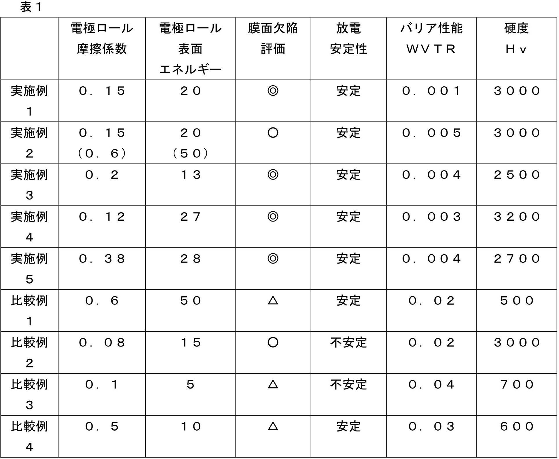
表1に示されるように、電極ロールの摩擦係数および表面エネルギーが本発明の規定範囲を満たしている実施例は、得られたガスバリア性フィルムの膜面欠陥が低減され、優れたガスバリア性を示した。これに対して、電極ロールの摩擦係数および表面エネルギーが本発明の規定範囲を上回っている比較例1は、膜面欠陥が発生し、ガスバリア性に劣った結果となった。また、電極ロールの表面エネルギーが本発明の規定範囲を外れている比較例3、および、摩擦係数が本発明の規定範囲を外れている比較例2および比較例4は、ガスバリア性に劣ることが分かった。また、比較例2はダイヤモンドライクカーボンの厚さのため放電が不安定となったと考えられる。
なお、本出願は、2013年4月22日に出願された日本国特許出願第2013-089704号に基づいており、その開示内容は、参照により全体として引用されている。
Claims (6)
- 基材の少なくとも一方の面に膜を形成するプラズマCVD成膜装置であって、
磁場形成手段を備えた第一電極ロールと、
第一電極ロールに対向して配置された、磁場形成手段を備えた第二電極ロールと、
を備え、
前記第一電極ロールおよび第二電極ロールの少なくとも一方の表面エネルギーが10~30mN/mであり、かつ、摩擦係数が0.1~0.4であるプラズマCVD成膜装置。 - 前記少なくとも一方の電極ロールの表面の硬度が1000~4000Hvである請求項1に記載のプラズマCVD成膜装置。
- 前記少なくとも一方の電極ロールの表面がダイヤモンドライクカーボンでコーティングされている請求項1または2に記載のプラズマCVD成膜装置。
- 前記ダイヤモンドライクカーボンの厚みが50~1000nmである請求項3に記載のプラズマCVD成膜装置。
- 表面エネルギーが10~30mN/mであり、かつ、摩擦係数が0.1~0.4であるプラズマCVD成膜装置用電極ロール。
- 請求項1~4のいずれか一項に記載のプラズマCVD成膜装置を用いて、基材上にガスバリア層を成膜する工程を有するガスバリア性フィルムの製造方法。
Priority Applications (1)
| Application Number | Priority Date | Filing Date | Title |
|---|---|---|---|
| JP2015513722A JP6288082B2 (ja) | 2013-04-22 | 2014-04-17 | 成膜装置、電極ロールおよびガスバリア性フィルムの製造方法 |
Applications Claiming Priority (2)
| Application Number | Priority Date | Filing Date | Title |
|---|---|---|---|
| JP2013-089704 | 2013-04-22 | ||
| JP2013089704 | 2013-04-22 |
Publications (1)
| Publication Number | Publication Date |
|---|---|
| WO2014175170A1 true WO2014175170A1 (ja) | 2014-10-30 |
Family
ID=51791748
Family Applications (1)
| Application Number | Title | Priority Date | Filing Date |
|---|---|---|---|
| PCT/JP2014/060981 Ceased WO2014175170A1 (ja) | 2013-04-22 | 2014-04-17 | 成膜装置、電極ロールおよびガスバリア性フィルムの製造方法 |
Country Status (2)
| Country | Link |
|---|---|
| JP (1) | JP6288082B2 (ja) |
| WO (1) | WO2014175170A1 (ja) |
Cited By (1)
| Publication number | Priority date | Publication date | Assignee | Title |
|---|---|---|---|---|
| JP2018532677A (ja) * | 2015-10-02 | 2018-11-08 | コーニング インコーポレイテッド | ガラス表面を処理して粒子の付着を低下させる方法 |
Citations (2)
| Publication number | Priority date | Publication date | Assignee | Title |
|---|---|---|---|---|
| JP2011037587A (ja) * | 2009-08-11 | 2011-02-24 | Fuji Electric Holdings Co Ltd | 基板搬送位置制御装置 |
| JP2012097354A (ja) * | 2010-10-08 | 2012-05-24 | Sumitomo Chemical Co Ltd | 積層体の製造方法 |
-
2014
- 2014-04-17 WO PCT/JP2014/060981 patent/WO2014175170A1/ja not_active Ceased
- 2014-04-17 JP JP2015513722A patent/JP6288082B2/ja not_active Expired - Fee Related
Patent Citations (2)
| Publication number | Priority date | Publication date | Assignee | Title |
|---|---|---|---|---|
| JP2011037587A (ja) * | 2009-08-11 | 2011-02-24 | Fuji Electric Holdings Co Ltd | 基板搬送位置制御装置 |
| JP2012097354A (ja) * | 2010-10-08 | 2012-05-24 | Sumitomo Chemical Co Ltd | 積層体の製造方法 |
Cited By (1)
| Publication number | Priority date | Publication date | Assignee | Title |
|---|---|---|---|---|
| JP2018532677A (ja) * | 2015-10-02 | 2018-11-08 | コーニング インコーポレイテッド | ガラス表面を処理して粒子の付着を低下させる方法 |
Also Published As
| Publication number | Publication date |
|---|---|
| JP6288082B2 (ja) | 2018-03-07 |
| JPWO2014175170A1 (ja) | 2017-02-23 |
Similar Documents
| Publication | Publication Date | Title |
|---|---|---|
| JP5513959B2 (ja) | ガスバリア性積層フィルム | |
| WO2014123201A1 (ja) | ガスバリア性フィルム、およびその製造方法 | |
| WO2012046778A1 (ja) | プラズマcvd成膜による積層体の製造方法 | |
| WO2016056605A1 (ja) | 積層体の製造方法 | |
| US10385447B2 (en) | Laminated film and flexible electronic device | |
| JP6288082B2 (ja) | 成膜装置、電極ロールおよびガスバリア性フィルムの製造方法 | |
| JP2012081631A (ja) | 積層フィルム | |
| JP6569685B2 (ja) | 成膜装置及びガスバリアーフィルムの製造方法 | |
| JP6354302B2 (ja) | ガスバリア性フィルム | |
| JPWO2015083681A1 (ja) | ガスバリアーフィルム及びその製造方法 | |
| JPWO2015163358A1 (ja) | ガスバリアーフィルム及びその製造方法 | |
| JP6642587B2 (ja) | プラズマcvd成膜装置 | |
| JP6579098B2 (ja) | ガスバリア性フィルムの製造方法 | |
| JPWO2016132901A1 (ja) | ガスバリアーフィルム及びその製造方法 | |
| JPWO2015053189A1 (ja) | ガスバリアーフィルム及びその製造方法 | |
| JP6897567B2 (ja) | ガスバリアーフィルム | |
| WO2017104357A1 (ja) | プラズマcvd成膜装置用電極、電極の製造方法、プラズマcvd成膜装置および機能性フィルムの製造方法 | |
| WO2016159206A1 (ja) | ガスバリアーフィルム及びその製造方法 | |
| JP6888623B2 (ja) | ガスバリア性フィルムの製造方法 | |
| WO2016148029A1 (ja) | 成膜装置及びガスバリアーフィルムの製造方法 | |
| WO2016117223A1 (ja) | ガスバリアーフィルムの製造装置および製造方法 | |
| JP6593347B2 (ja) | ガスバリアフィルムの製造方法及び製造装置 | |
| JP2022138914A (ja) | ガスバリア性フィルムの製造方法及びその巻回体 | |
| JP2016211066A (ja) | 成膜ローラー及び成膜装置 | |
| WO2014109250A1 (ja) | 機能性フィルムの製造方法、機能性フィルム製造装置、および機能性フィルムを備える有機エレクトロルミネッセンス素子 |
Legal Events
| Date | Code | Title | Description |
|---|---|---|---|
| 121 | Ep: the epo has been informed by wipo that ep was designated in this application |
Ref document number: 14788344 Country of ref document: EP Kind code of ref document: A1 |
|
| ENP | Entry into the national phase |
Ref document number: 2015513722 Country of ref document: JP Kind code of ref document: A |
|
| NENP | Non-entry into the national phase |
Ref country code: DE |
|
| 122 | Ep: pct application non-entry in european phase |
Ref document number: 14788344 Country of ref document: EP Kind code of ref document: A1 |