WO2014171394A1 - 照明装置、照明機器および表示装置 - Google Patents
照明装置、照明機器および表示装置 Download PDFInfo
- Publication number
- WO2014171394A1 WO2014171394A1 PCT/JP2014/060413 JP2014060413W WO2014171394A1 WO 2014171394 A1 WO2014171394 A1 WO 2014171394A1 JP 2014060413 W JP2014060413 W JP 2014060413W WO 2014171394 A1 WO2014171394 A1 WO 2014171394A1
- Authority
- WO
- WIPO (PCT)
- Prior art keywords
- led
- light
- phosphor
- light source
- led chip
- Prior art date
- Legal status (The legal status is an assumption and is not a legal conclusion. Google has not performed a legal analysis and makes no representation as to the accuracy of the status listed.)
- Ceased
Links
Images











Classifications
-
- G—PHYSICS
- G02—OPTICS
- G02B—OPTICAL ELEMENTS, SYSTEMS OR APPARATUS
- G02B6/00—Light guides; Structural details of arrangements comprising light guides and other optical elements, e.g. couplings
- G02B6/0001—Light guides; Structural details of arrangements comprising light guides and other optical elements, e.g. couplings specially adapted for lighting devices or systems
- G02B6/0011—Light guides; Structural details of arrangements comprising light guides and other optical elements, e.g. couplings specially adapted for lighting devices or systems the light guides being planar or of plate-like form
- G02B6/0081—Mechanical or electrical aspects of the light guide and light source in the lighting device peculiar to the adaptation to planar light guides, e.g. concerning packaging
- G02B6/0086—Positioning aspects
- G02B6/009—Positioning aspects of the light source in the package
-
- G—PHYSICS
- G02—OPTICS
- G02B—OPTICAL ELEMENTS, SYSTEMS OR APPARATUS
- G02B6/00—Light guides; Structural details of arrangements comprising light guides and other optical elements, e.g. couplings
- G02B6/0001—Light guides; Structural details of arrangements comprising light guides and other optical elements, e.g. couplings specially adapted for lighting devices or systems
- G02B6/0011—Light guides; Structural details of arrangements comprising light guides and other optical elements, e.g. couplings specially adapted for lighting devices or systems the light guides being planar or of plate-like form
- G02B6/0066—Light guides; Structural details of arrangements comprising light guides and other optical elements, e.g. couplings specially adapted for lighting devices or systems the light guides being planar or of plate-like form characterised by the light source being coupled to the light guide
- G02B6/0068—Arrangements of plural sources, e.g. multi-colour light sources
-
- G—PHYSICS
- G02—OPTICS
- G02B—OPTICAL ELEMENTS, SYSTEMS OR APPARATUS
- G02B6/00—Light guides; Structural details of arrangements comprising light guides and other optical elements, e.g. couplings
- G02B6/0001—Light guides; Structural details of arrangements comprising light guides and other optical elements, e.g. couplings specially adapted for lighting devices or systems
- G02B6/0011—Light guides; Structural details of arrangements comprising light guides and other optical elements, e.g. couplings specially adapted for lighting devices or systems the light guides being planar or of plate-like form
- G02B6/0013—Means for improving the coupling-in of light from the light source into the light guide
- G02B6/0023—Means for improving the coupling-in of light from the light source into the light guide provided by one optical element, or plurality thereof, placed between the light guide and the light source, or around the light source
- G02B6/0026—Wavelength selective element, sheet or layer, e.g. filter or grating
-
- G—PHYSICS
- G02—OPTICS
- G02B—OPTICAL ELEMENTS, SYSTEMS OR APPARATUS
- G02B6/00—Light guides; Structural details of arrangements comprising light guides and other optical elements, e.g. couplings
- G02B6/0001—Light guides; Structural details of arrangements comprising light guides and other optical elements, e.g. couplings specially adapted for lighting devices or systems
- G02B6/0011—Light guides; Structural details of arrangements comprising light guides and other optical elements, e.g. couplings specially adapted for lighting devices or systems the light guides being planar or of plate-like form
- G02B6/0066—Light guides; Structural details of arrangements comprising light guides and other optical elements, e.g. couplings specially adapted for lighting devices or systems the light guides being planar or of plate-like form characterised by the light source being coupled to the light guide
- G02B6/0073—Light emitting diode [LED]
-
- G—PHYSICS
- G02—OPTICS
- G02B—OPTICAL ELEMENTS, SYSTEMS OR APPARATUS
- G02B6/00—Light guides; Structural details of arrangements comprising light guides and other optical elements, e.g. couplings
- G02B6/0001—Light guides; Structural details of arrangements comprising light guides and other optical elements, e.g. couplings specially adapted for lighting devices or systems
- G02B6/0011—Light guides; Structural details of arrangements comprising light guides and other optical elements, e.g. couplings specially adapted for lighting devices or systems the light guides being planar or of plate-like form
- G02B6/0081—Mechanical or electrical aspects of the light guide and light source in the lighting device peculiar to the adaptation to planar light guides, e.g. concerning packaging
- G02B6/0086—Positioning aspects
- G02B6/0091—Positioning aspects of the light source relative to the light guide
-
- F—MECHANICAL ENGINEERING; LIGHTING; HEATING; WEAPONS; BLASTING
- F21—LIGHTING
- F21Y—INDEXING SCHEME ASSOCIATED WITH SUBCLASSES F21K, F21L, F21S and F21V, RELATING TO THE FORM OR THE KIND OF THE LIGHT SOURCES OR OF THE COLOUR OF THE LIGHT EMITTED
- F21Y2105/00—Planar light sources
-
- F—MECHANICAL ENGINEERING; LIGHTING; HEATING; WEAPONS; BLASTING
- F21—LIGHTING
- F21Y—INDEXING SCHEME ASSOCIATED WITH SUBCLASSES F21K, F21L, F21S and F21V, RELATING TO THE FORM OR THE KIND OF THE LIGHT SOURCES OR OF THE COLOUR OF THE LIGHT EMITTED
- F21Y2115/00—Light-generating elements of semiconductor light sources
- F21Y2115/10—Light-emitting diodes [LED]
-
- G—PHYSICS
- G02—OPTICS
- G02B—OPTICAL ELEMENTS, SYSTEMS OR APPARATUS
- G02B6/00—Light guides; Structural details of arrangements comprising light guides and other optical elements, e.g. couplings
- G02B6/0001—Light guides; Structural details of arrangements comprising light guides and other optical elements, e.g. couplings specially adapted for lighting devices or systems
- G02B6/0011—Light guides; Structural details of arrangements comprising light guides and other optical elements, e.g. couplings specially adapted for lighting devices or systems the light guides being planar or of plate-like form
- G02B6/0081—Mechanical or electrical aspects of the light guide and light source in the lighting device peculiar to the adaptation to planar light guides, e.g. concerning packaging
- G02B6/0083—Details of electrical connections of light sources to drivers, circuit boards, or the like
-
- H—ELECTRICITY
- H10—SEMICONDUCTOR DEVICES; ELECTRIC SOLID-STATE DEVICES NOT OTHERWISE PROVIDED FOR
- H10H—INORGANIC LIGHT-EMITTING SEMICONDUCTOR DEVICES HAVING POTENTIAL BARRIERS
- H10H20/00—Individual inorganic light-emitting semiconductor devices having potential barriers, e.g. light-emitting diodes [LED]
- H10H20/80—Constructional details
- H10H20/85—Packages
- H10H20/851—Wavelength conversion means
- H10H20/8511—Wavelength conversion means characterised by their material, e.g. binder
- H10H20/8512—Wavelength conversion materials
- H10H20/8513—Wavelength conversion materials having two or more wavelength conversion materials
-
- H—ELECTRICITY
- H10—SEMICONDUCTOR DEVICES; ELECTRIC SOLID-STATE DEVICES NOT OTHERWISE PROVIDED FOR
- H10W—GENERIC PACKAGES, INTERCONNECTIONS, CONNECTORS OR OTHER CONSTRUCTIONAL DETAILS OF DEVICES COVERED BY CLASS H10
- H10W90/00—Package configurations
Definitions
- a plurality of LEDs 212 each having two LED chips mounted in one package are mounted on the substrate 202.
- the LED 212 can be regarded as an LED in which the LEDs 203 and 204 are packaged. Therefore, the LED 212 emits light of two different colors similar to the light from the LEDs 203 and 204.
- the illuminating device 211 when two outgoing lights from the LED 212 enter the light guide plate 205, a part of the color is mixed in front of the LED 212. However, the other emitted lights are not mixed in the regions B3 and B4 until they are mixed with the emitted light from the adjacent LEDs 212. Therefore, according to the illuminating device 211, the width
- Mutual absorption means that when the electrons in the ground state of the valence band absorb incident light, light emitted from one LED chip is adjacent due to absorption of light when transitioning between bands to the excited state of the conduction band. This is a phenomenon absorbed by the other LED chip.
- an illumination device includes a light guide plate, a substrate, and a plurality of LED chips arranged on the substrate, and light emitted from the LED chip is guided.
- a light source portion disposed so as to be incident on the light incident portion of the light plate, and the LED chip is disposed so as to form a plurality of rows on the substrate, and the rows between the rows, It is characterized by being arranged in an orthogonal direction.
- (A) is a top view which expands and shows a part of light source part in the illuminating device which concerns on Embodiment 5 of this invention
- (b) is a longitudinal cross-sectional view of the said illuminating device. It is a perspective view of the liquid crystal display device which concerns on Embodiment 6 of this invention. It is a perspective view of the ceiling light which concerns on Embodiment 7 of this invention.
- (A) is a front view which expands and shows a part of the conventional illuminating device using LED of different luminescent color
- (b) is a top view which expands and shows a part of light source part in the said illuminating device. is there.
- Embodiment 1 of the present invention will be described with reference to FIGS.
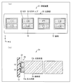
- FIG. 1A is an enlarged plan view showing a part of the light source unit 10 in the illumination device 11 according to Embodiment 1, and FIG. 1B is a longitudinal sectional view of the illumination device 11. As shown in FIG.
- the lighting device 11 includes a substrate 12, a plurality of LEDs 13 and 14, and a light guide plate 15.
- the light guide plate 15 is a transparent member that is formed in a rectangular shape and has a predetermined thickness.
- the light guide plate 15 has a structure capable of extracting light from each part of the light emitting surface 15b so as to emit light incident from the light incident part 15a in a planar shape, and is formed of a transparent material such as acrylic. Yes. Further, the end surface on one side of the light guide plate 15 functions as a light incident portion 15a on which light is incident.
- the substrate 12 and the LEDs 13 and 14 constitute a light source unit 10.
- the light source unit 10 has the light emitting surfaces of the LEDs 13 and 14 facing the light incident part 15a so that the light emitted from the LED chips 16 of the LEDs 13 and 14 enters the light incident part 15a of the light guide plate 15, and It is arranged at a position close to the light guide plate 15.
- the LEDs 13 and 14 have a rectangular light emitting surface, and the LED chip 16 is mounted in the center.
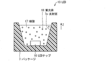
- the LED 13 includes a package 7, an LED chip 16, a resin 17, and a phosphor 18.
- the package 7 has a reflection surface 7a that forms the side surface of the concave portion.
- the reflecting surface 7a is preferably formed of a highly reflective Ag or Al-containing metal film or white silicone so that light emitted from the LED chip 16 is reflected to the outside of the LED 13. Further, the reflection surface 7a is formed so as to be inclined with respect to the light emitted from the LED chip 16 that goes straight in the Z direction in front of the emission, that is, the light having an emission angle of 0 °.
- the LED chip 16 (LED element) is, for example, a GaN-based semiconductor light-emitting element having a conductive substrate. Although not shown, a bottom electrode is formed on the bottom surface of the conductive substrate, and an upper electrode is formed on the opposite surface. Is formed.
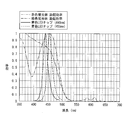
- the emitted light (primary light) of the LED chip 16 is blue light in the range of 430 to 480 nm and has a peak wavelength near 450 nm.
- the LED chip 16 (blue LED chip) is die-bonded with a conductive brazing material on one side of the exposed portion of the lead frame. Further, in the LED chip 16, the upper electrode of the LED chip 16 and the other side of the exposed portion of the lead frame are wire-bonded with a wire (not shown). Thus, the LED chip 16 is electrically connected to the lead frame.
- the LED chip having the electrodes on the upper surface and the lower surface is described, but an LED chip having two electrodes on the upper surface may be used.
- Resin 17 is filled in the recesses to seal the recesses where the LED chips 16 are disposed. Further, since the resin 17 is required to have high durability against the primary light having a short wavelength, a silicone resin is preferably used. The surface of the resin 17 forms a light emitting surface from which light is emitted.
- the phosphor 18 (red phosphor) is dispersed in the resin 17.
- the phosphor 18 is a red phosphor that emits red light having a longer wavelength than the primary light (peak wavelength is 600 nm or more and 780 nm or less).
- a phosphor material in which CaAlSiN 3 : Eu is mixed, K 2 SiF 6 : Made of phosphor material (KSF) mixed with Mn for example, a phosphor material in which CaAlSiN 3 : Eu is mixed, K 2 SiF 6 : Made of phosphor material (KSF) mixed with Mn.
- the LED 13 configured as described above, as the primary light (blue light) emitted from the LED chip 16 passes through the resin 17, a part thereof excites the phosphor 18 and secondary light (red light). Is converted to As described above, the LED 13 emits magenta light by mixing the blue primary light and the red secondary light.
- the LED drive control unit 1 includes a dimming control unit 2, constant current circuits 3 and 4, and LED circuits 5 and 6.
- the LED circuit 5 is a series circuit of LEDs 13 mounted on the substrate 12.
- the LED circuit 6 is a series circuit of LEDs 14 mounted on the substrate 12.
- the constant current circuit 3 controls the constant current that flows to the LED circuit 5 by the PWM signal that the dimming control unit 2 individually controls.
- the constant current flowing through the circuit 6 is controlled.
- the light intensity of LED13,14 is controlled separately. Therefore, the light source unit 10 can irradiate the light guide plate 15 with mixed color light having different colors according to the light intensity of each of the LEDs 13 and 14 by adjusting the constant current flowing through the LED circuits 5 and 6. it can.
- the LEDs 13 and 14 are disposed near the end on the light emitting surface 15b side and the end on the back side facing the light emitting surface 15b in the light incident portion 15a of the light guide plate 15. Thereby, when the light emitted from the LEDs 13 and 14 is incident on the light guide plate 15, the light is immediately totally reflected on the surface of the light guide plate 15. Thus, the reduction of the color mixing distance also contributes to the improvement of the color mixing property.
- the reflection surface 7a of the package 7 is inclined, the light emitted from the LED chip 16 is reflected by the reflection surface 7a, and the emission angle of the light emitted from the opening of the package 7 is increased. This improves the extraction rate of light emitted from the opening of the package 7 and contributes to shortening the color mixing distance.
- Embodiment 2 of the present invention will be described with reference to FIGS. 4 to 13 and FIGS. 26 to 30.
- FIG. 4 to 13 Embodiment 2 of the present invention will be described with reference to FIGS. 4 to 13 and FIGS. 26 to 30.
- FIG. 5A is an enlarged plan view showing a part of the light source unit 20 in the illumination device 21 according to the second embodiment
- FIG. 5B is a longitudinal sectional view of the illumination device 21.
- a plurality of LEDs 22 are mounted on the substrate 12 so as to be arranged in a line along the longitudinal direction (X direction) of the substrate 12. Further, the LED 22 has two LED chips 16 arranged at a distance from each other.
- the LED 22 in the light source unit 20 is configured as an LED 22A, for example, as shown in FIG.
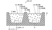
- the LED 22A includes a package 23, two LED chips 16, a resin 17, and phosphors 18 and 19.
- the package 23 has two concave portions that form a mortar shape that spreads from the bottom surface to the opening.
- One LED chip 16 is mounted on the bottom surface of each concave surface portion.
- Each concave surface portion forms a space (concave portion) for filling the resin 17.
- the package 23 is formed of a nylon material, like the package 7 in the first embodiment, and is provided by insert molding so that a lead frame (not shown) is exposed on the bottom surface of the concave portion.
- the lead frame is divided into two parts at two exposed portions.
- the package 23 also has reflection surfaces 23a and 23b that form the side surfaces of the concave portion.
- the reflecting surfaces 23a and 23b are preferably formed of a metal film or white silicon containing Ag or Al having a high reflectivity so as to reflect the light emitted from the LED chip 16 to the outside of the LED 22A. Further, the reflection surfaces 23a and 23b are formed so as to be inclined with respect to the light emitted from the LED chip 16 that goes straight in the Z direction in front of the emission, that is, the light with the emission angle of 0 °.
- the package 23 has a partition wall 23c between two concave portions. Light emitted from the two LED chips 16 is blocked between the two LED chips 16 in the LED 22A by the partition wall 23c. That is, the two LED chips 16 are optically separated by the partition wall 23c.
- the light source unit 20 emits white light by mixing the magenta light and the cyan light.
- FIG. 7A is an enlarged front view showing a part of the color mixture state in the lighting device 21, and FIG. 7B is a longitudinal sectional view of the lighting device 21.
- the emitted light from the LED 22 does not appear to be mixed in the regions A ⁇ b> 1 and A ⁇ b> 2 in the light guide plate 15.
- the light emission surface 15b of the light guide plate 15 appears to be mixed in the Y direction (the thickness direction of the light guide plate 15).
- the LED chip 16 in the LED 22 is disposed in the light incident portion 15a of the light guide plate 15 near the end on the light emitting surface 15b side and the end on the back side facing the light emitting surface 15b.
- the reduction of the color mixing distance L1 also contributes to the improvement of the color mixing property.
- the reflection surfaces 23a and 23b of the package 23 are inclined, the emission angle of the light emitted from the LED chip 16 reflected by the reflection surfaces 23a and 23b and emitted from the opening of the package 23 is increased. . This improves the light extraction efficiency emitted from the opening of the package 23 and contributes to shortening the color mixing distance L1.
- the mounting width of the LED 22 (LED 22A) on the substrate 12 can be reduced.
- variety of the light-incidence part 15a determined according to the said mounting width can be narrowed, and the light-guide plate 15 can be formed thinly.
- two LED chips 16 are mounted on the substrate 12 at once.
- the manufacturing cost of the illuminating device 21 can be reduced.
- the LED chips 16A and 16B are different from each other so that their respective peak wavelengths match the optimum excitation wavelengths of the phosphors 18 and 19.
- the peak wavelength of the LED chip 16A that excites the phosphor 18 red phosphor
- the peak wavelength of the LED chip 16B that excites the phosphor 19 green phosphor
- the phosphor 18 is excited at the optimum excitation wavelength at which the excitation efficiency reaches a peak
- the phosphor 19 is excited at the optimum excitation wavelength at which the excitation efficiency is maximized with respect to the lower limit value of the peak wavelength of the blue LED chip. Therefore, loss of light emission by the phosphors 18 and 19 can be suppressed. Therefore, the luminous efficiency of the LED 22 can be improved.
- FIG. 10 is a longitudinal sectional view of an LED 22C (third LED) on which the blue LED chip 16 is mounted in the illumination device 21.
- FIG. 11 is a graph showing a black body radiation curve for specifying two luminescent colors obtained by the LED 22C as two points of chromaticity.
- the light source unit 20 may have an LED 22C shown in FIG. 10 instead of the above-described LED 22A.
- the LED 22C includes the package 23, the two LED chips 16, the resin 17, and the phosphors 18 and 19 as well as the LED 22A, but further includes a phosphor 24.
- various white colors can be emitted by mixing two different color temperatures.
- various white colors can be obtained by changing the mixing ratio and mixing amount of the phosphors 18, 19, and 24 to the resin 17. Further, by controlling the constant current applied to the two LED chips 16 in the LED 22C by the LED drive control unit 1 shown in FIG. 4 and adjusting the light intensity of each LED chip 16, the color temperatures of the two colors are different. Any intermediate color can be obtained based on white.
- FIG. 12 is a longitudinal sectional view of an LED 22D (fourth LED) on which the blue LED chip 16 and the green LED chip 25 are mounted in the lighting device 21.
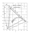
- FIG. 13 is a chromaticity diagram showing the chromaticity point of the green LED chip 25 in the LED 22D and the chromaticity point of the green phosphor in the conventional LED.
- the LED 22D is different from the LED 22A in that the LED chip 25 is mounted and filled with the resin 17 in the first light source LS1 formed in one recess of the package 23, but the phosphor is not dispersed. Further, in the second light source LS2 formed in the other concave portion of the LED 22D, the phosphor 18 is dispersed in the resin 17 to be filled.
- the LED chip 25 (green LED chip) is a GaN-based green LED.
- the emitted light (primary light) of the LED chip 25 is green light in the range of 510 to 630 nm, and has a peak wavelength near 560 nm.
- the green light emitted from the green LED chip 25 is obtained by the first light source LS1, while the blue light from the blue LED chip 16 and the phosphor 18 are emitted from the second light source LS2.
- Magenta light is obtained as a mixed color of red light.
- white light is obtained by the mixed color of green light and magenta light.
- the chromaticity point of the green light emitted from the green phosphor is located inside the chromaticity point chromaticity coordinates of the green LED light as shown in FIG.
- the area of the triangle defined by the chromaticity point of the green light emitted from the green phosphor is smaller than the area of the triangle when the LED chip 25 is used, as shown by the solid line. Therefore, the color reproducibility when the green phosphor is used is inferior to the color reproducibility when the LED chip 25 is used.
- the green LED chip 25 rather than the green phosphor.
- the chromaticity of red when the red phosphor is used and when the red LED chip is used, when the red LED chip is used, the chromaticity coordinates of the chromaticity points are located on the outer side. Therefore, the color reproducibility becomes higher. Therefore, in the LED 22D, a red LED chip may be mounted instead of the LED chip 25, and the red phosphor 18 may be replaced with the green phosphor 19 (the blue LED chip 16 and the green phosphor 19 may be replaced with each other). combination). Thereby, color reproducibility can be improved like said LED22D.
- FIG. 26 is a longitudinal sectional view of an LED 22E (fifth LED) on which the blue LED chip 16 is mounted in the illumination device 21.
- FIG. 27 is an xy chromaticity diagram showing the illumination color of the LED 22E.
- the first light source LS1 formed in one recess of the package 23 and the second light source LS2 formed in the other recess have the same phosphors 18 and 19 dispersed in the resin 17. Yes.
- the first light source LS ⁇ b> 1 and the second light source LS ⁇ b> 2 emit light of different colors when the mixing ratios and mixing amounts of the phosphors 18 and 19 are different.
- the first light source LS1 emits white light with a color temperature of 5000K
- the second light source LS2 emits orange-pink light.
- orange-pink light can be obtained by adjusting the mixing ratio and mixing amount of the phosphors 18 to be larger than the mixing ratio and mixing amount of the phosphors 19 (increasing the red component). .
- the “orange pink color” corresponds to the light source color defined by the JIS (Japanese Industrial Standard) standard (JIS Z 8110).
- the chromaticity range of the light source it is only necessary to realize the chromaticity in the region S as long as the effect of promoting sleep is noted.
- the color difference is a level that cannot be discerned by human eyes if the variation in chromaticity is within the range of the MacAdam ellipse 3-step.
- the LED 22E can emit light of this chromaticity.
- Patent Document 5 Japanese Patent Application Laid-Open No. 2013-171687
- this luminescent color is a color that can reduce human fatigue and improve work efficiency.
- the LED drive control unit 1 controls the lighting of the first light source LS1 and the second light source LS2 as follows.
- the first light source LS1 when obtaining daylight white light, the first light source LS1 is turned on and the second light source LS2 is turned off. When obtaining orange-pink light, the first light source LS1 is turned off and the second light source LS2 is turned on. In addition, when obtaining light having a color of a chromaticity point between daylight white and orange pink, the first light source LS1 and the second light source LS2 are adjusted so that the ratio of the respective light fluxes (lumens) is adjusted. The lighting of the first light source LS1 and the second light source LS2 is controlled.
- the ratio of luminous fluxes (lumens) of the first light source LS1 and the second light source LS2 is about 1:
- the first light source LS1 and the second light source LS2 are turned on so as to be 1.16 (day white: orange pink).
- the ratio of the luminous flux amounts of the first light source LS1 and the second light source LS2 varies depending on the types of optical materials used for the phosphors 18 and 19, the light guide plate 15, and the like. Therefore, the ratio of the luminous flux when obtaining the light of the above color is only an example.
- the above-described GaN-based semiconductor light-emitting element is used as the LED chip 16 (peaking at around 450 nm)
- the above-described CaAlSiN 3 : Eu is used as the phosphor 18
- Eu-activated ⁇ sialon is used as the phosphor 19.
- the emission ratios of the first light source LS1 and the second light source LS2 are respectively set by appropriately setting the mixing ratio and the mixing amount of the phosphors 18 and 19.
- the above-described emission colors of the first light source LS1 and the second light source LS2 are colors other than the daylight white color and the orange pink color described above.
- the line is extended, and the emission colors of the first light source LS1 and the second light source LS2 are set at chromaticity points near the coordinates on the extended line.
- the first light source LS1 and the second light source LS2 can be used to adjust the emission color including the daylight white light and the orange pink color.
- the phosphor 18A is made of a forbidden transition type phosphor material, for example, a phosphor material (KSF) mixed with the aforementioned K 2 SiF 6 : Mn.
- the phosphor 18B is made of an allowable transition type phosphor material, for example, a phosphor material (CASN) mixed with the aforementioned CaAlSiN 3 : Eu.
- the phosphor 18A of the first light source LS1 a forbidden transition type phosphor material having a narrow spectrum and good color rendering but a slow response speed (ms order) is used.
- a forbidden transition type phosphor material having a narrow spectrum and good color rendering but a slow response speed (ms order) is used.
- an allowable transition type phosphor material having a high response speed ( ⁇ s order) is used.
- the light amount of the first light source LS1 is controlled to be larger than the light amount of the second light source LS2.
- the afterglow is reduced, the light amount of the second light source LS2 is controlled to be larger than the light amount of the first light source LS1.
- the reduction in afterglow is effective for a backlight for a liquid crystal TV in which a case where a backlight dimming frequency (PWM) is used at 240 Hz or less (3D display or backlight scanning) is assumed.
- PWM backlight dimming frequency
- KSF fluorescent substance and CASN fluorescent substance were demonstrated as red fluorescent substance 18A, 18B used in LED22E, it is not limited to these.
- an SCASN phosphor or an ⁇ SiAlON phosphor may be used instead of the CASN phosphor as an allowable transition type phosphor material.
- the SCASN phosphor and the ⁇ SiAlON phosphor are represented by the following chemical formulas.
- a red phosphor substance shown in an eighth embodiment described later may be used as the forbidden transition type phosphor material.
- the red phosphor 18A is dispersed in the resin 17 of the first light source LS1 and the resin of the second light source LS2 as in the LED 22E according to the second configuration. 17 is dispersed with a red phosphor 18B.
- the green phosphor 19A is dispersed in the resin 17 of the first light source LS1
- the green phosphor 19B is dispersed in the resin 17 of the second light source LS2.
- the phosphors 18A and 18B are made of the same phosphor material as the phosphor material used in the LED 22E according to the second configuration.
- the phosphor 18B may be made of a phosphor material other than the above CASN as long as it is an allowable transition type phosphor material.
- the phosphor 19A is made of a phosphor material of Mn activated ⁇ -AlON.
- the phosphor 19B is made of the above-described Eu-activated ⁇ sialon phosphor material.
- the phosphor 18A of the first light source LS1 is a forbidden transition type fluorescence having a narrow spectrum and good color rendering but a slow response speed.
- a body material is used, and an acceptable transition type phosphor material having a high response speed is used as the phosphor 18B of the second light source LS2.
- the characteristics of the phosphors 18A and 18B are different, light having different characteristics can be obtained by controlling the light amounts of the first light source LS1 and the second light source LS2 according to conditions.
- the phosphor 19A is made of a phosphor material having a slow response speed
- the phosphor 19B is made of a phosphor material having a fast response speed.
- the order levels of the response speeds of the phosphors 18A and 19 in the first light source LS1 are different, and the order levels of the response speeds of the phosphors 18B and 19 in the second light source LS2 are different.
- the afterglow characteristics of the phosphors 18A and 18B are different, the use of the high color rendering display and the afterglow reduction display as described above may be hindered. There is no.
- the light source unit 20 may have an LED 22F shown in FIG. 28 instead of the above-described LED 22A.
- This LED 22F has a package 23, a resin 17 and a phosphor 18 like the LED 22A.
- the LED 22F includes LED chips 16C and 16D instead of the LED chip 16 in the LED 22A.
- the output light from the LED chip 16C has higher excitation efficiency for the phosphors 18 and 19 than the output light from the LED chip 16D. Most of the light energy output from the LED chip 16C is consumed to excite the phosphors 18 and 19, and the first light source mainly emits red light and green light.
- the blue light of the second light source LS2 does not excite the phosphors 18 and 19 of the first light source LS1. .
- the blue light of the second light source LS2 is not absorbed by the phosphors 18 and 19, the light emission efficiency of the second light source LS2 can be maintained satisfactorily.
- the blue light of the second light source LS2 does not affect the light emission of the phosphors 18, 19, the chromaticity adjustment of the first light source LS1 is easy.
- the peak wavelength of the LED chip 16C is 350 nm or more and 410 nm or less (blue light to near ultraviolet light), and the peak wavelength of the LED chip 16D is a predetermined range centered at 445 nm (around 445 nm). It is.
- the LED chip 16C Since these phosphors are excited by the output light of the LED chip 16C that emits light with a peak wavelength of 350 nm or more and 410 nm or less, rather than combining with the LED chip 16 having a peak wavelength near 450 nm exemplified in the first embodiment, It can emit red and green efficiently. Most of the light energy output from the LED chip 16C is consumed to excite the phosphors 18 and 19, and the first light source LS1 mainly emits red light and green light. In contrast, the second light source LS2 emits blue light having a peak wavelength of about 445, which is output light from the LED chip 16D.
- the second light source LS2 emits light at a slightly shorter wavelength than the blue light having a peak in the vicinity of 450 nm exemplified in Embodiment 1, the color gamut that can be expressed in blue is expanded. Further, when the LED 22F is used for the backlight of the liquid crystal display device, the overlap of the emission spectra of the LED chip 16 and the phosphor 19 of the first light source LS1 is reduced. Thereby, since color separation by the color filter of the liquid crystal display panel is improved, the green color gamut can be expanded. Furthermore, by selecting a phosphor having an emission wavelength as short as 1 to 5 nm as the green phosphor 19, it is possible to expand the entire color gamut of blue, green and red.
- the LED 22F according to the second configuration can be suitably used for a display device that requires high luminance.
- blue light emitted from the LED chip 16D if blue light having a light peak wavelength of around 445 nm, for example, in the range of 440 to 450 nm, or in the range of 430 nm to 450 nm, is selected, the effect of expanding the color gamut as described above can be obtained. can get.
- FIG. 29A is an enlarged plan view showing a part of another light source unit 20A including the LED 22G (seventh LED) in the illumination device 21 according to the second embodiment.
- FIG. 29B is an enlarged plan view showing a part of the light source unit 20B including another LED 22G in the illumination device 21.
- FIG. 29A is an enlarged plan view showing a part of another light source unit 20A including the LED 22G (seventh LED) in the illumination device 21 according to the second embodiment.
- FIG. 29B is an enlarged plan view showing a part of the light source unit 20B including another LED 22G in the illumination device 21.
- the light amount of the second light source LS2 can be made larger than the light amount of the first light source LS1. This is effective when, for example, toning light is performed by changing the light amounts of the first light source LS1 and the second light source LS2.
- the light intensity of the LED chip 16D is higher than the light intensity of the LED chip 16C. Since the LED chip 16C emits a wavelength with good excitation efficiency of the phosphors 18 and 19, the light intensity of green light and red light mainly output from the first light source LS1 is high. Accordingly, by increasing the intensity of the blue light output from the second light source LS2, the luminance of the white light obtained by mixing the light output from the first light source LS1 and the second light source LS2 is also improved. Therefore, it is possible to improve the luminance of the LED 22F that reduces blue light.
- FIG. 30 is a plan view of the LED 22H (eighth LED).
- the package 23 has a cathode mark 23d.
- the cathode mark 23d is formed on the same short side of the package 23 so that one corner of the first light source LS1 and the second light source LS2 in the package 23 is missing.
- each of the LEDs 22B to 22H described above is configured in one package 23.
- each of the LEDs 22B to 22H may be configured as two separate LEDs like the LEDs 13 and 14 in the first embodiment.
- Embodiment 3 of the present invention will be described with reference to FIGS. 4, 14 and 15.
- FIG. 14A is an enlarged plan view showing a part of the light source unit 30 in the illumination device 31 according to the third embodiment, and FIG. 14B is a longitudinal sectional view of the illumination device 31.
- the lighting device 31 includes a substrate 12, a light guide plate 15, and a plurality of LEDs 32.
- a plurality of LEDs 32 are mounted on the substrate 12 in two rows along the longitudinal direction of the substrate 12. In each row, the LEDs 32 are electrically connected in series. Further, the LEDs 32 are arranged at intervals between adjacent rows so that the respective LED chips 16 are arranged in a direction (Y direction) orthogonal to the row direction (X direction).
- the LED chips 16 arranged in the same row are electrically connected in series and constitute the above-described LED circuits 5 and 6, respectively. Thereby, the LED chip 16 which comprises each row
- the substrate 12 and the LED 32 constitute a light source unit 30.
- the light source unit 30 has the light emitting surface of the LED 32 opposed to the light incident part 15a so that the light emitted from each LED chip 16 of the LED 32 enters the light incident part 15a of the light guide plate 15, and It is arranged at a close position.
- FIG. 15 is a longitudinal sectional view of the LED 32 in the illumination device 31.
- the LED 32 has a rectangular light emitting surface, and the LED chip 16 is mounted in the center. As shown in FIG. 15, the LED 32 includes a package 7, an LED chip 16, a resin 17, and phosphors 18 and 19.
- This LED 32 is different from the LEDs 13 and 14 in the first embodiment in that the phosphors 18 and 19 are dispersed in the resin 17 filled in both concave portions of the package 7.
- the LED 32 configured as described above, as the primary light (blue light) emitted from the LED chip 16 passes through the resin 17, a part thereof excites the phosphors 18 and 19 to secondary light (red). Light and green light). In this way, the LED 13 emits white light to the outside by mixing the blue primary light and the red and green secondary lights.
- said LED32 combines the blue LED chip
- the LED 32 may be configured by combining a blue LED chip 16 and a yellow phosphor, and can obtain a pseudo luminescent color.
- the LED 32 since the LED 32 includes the LED chip 16 independently, it is possible to prevent mutual absorption of light between the LED chips 16. Thereby, the fall of the luminous efficiency of LED32 can be suppressed.
- the shape of the light emitting surface of the LED 32 is rectangular, and since the longitudinal direction of the light emitting surface and the longitudinal direction of the substrate 12 are the same direction, they can be arranged on the elongated substrate 12 in the width direction of the substrate 12. Further, with such a shape, the directivity characteristics of the LED 32 are wide in the long side direction of the light emitting surface of the LED 32 and narrow in the short side direction. Thereby, since the light to the light incident part 15a is narrowed and incident with respect to the width direction of the light incident part 15a, the light incident characteristic to the light guide plate 15 is improved.
- the LED 32 combines the blue LED chip 16 with the red phosphor 18 and the green phosphor 19, white light with good color rendering properties (color reproducibility) can be obtained. Moreover, light having an arbitrary chromaticity on the chromaticity coordinates can be generated by the blending ratio of the phosphors 18 and 19.
- FIG. 16A is an enlarged plan view showing a part of the light source unit 40 in the illumination device 41 according to the fourth embodiment, and FIG. 16B is a longitudinal sectional view of the illumination device 41.
- the lighting device 41 includes a substrate 12, a light guide plate 15, and a plurality of LEDs 42.
- a plurality of LEDs 42 are mounted on the substrate 12 so as to be arranged in a line along the longitudinal direction (X direction) of the substrate 12.
- the LED 42 includes two LED chips 16 that are spaced apart from each other.
- the substrate 12 and the LED 42 constitute a light source unit 40.
- the light emitting surface of the LED 42 faces the light incident part 15 a so that the respective emitted light of the two LED chips 16 in the LED 42 enters the light incident part 15 a of the light guide plate 15, and the light guide plate 15. It is arranged at a position close to.
- FIG. 17 is a longitudinal sectional view of the LED 42 in the illumination device 41.
- the LED 42 includes a package 23, two LED chips 16, a resin 17, and phosphors 18 and 19.
- the phosphors 18 and 19 are dispersed not only in the resin 17 filled in one recess in the package 23 but also in the resin 17 filled in the other recess. .
- the LED 42 is a combination of the blue LED chip 16, the red phosphor 18, and the green phosphor 19, similar to the LED 32 in the third embodiment, but the combination is not limited to this.
- the LED 42 may be configured by combining a blue LED chip 16 and a yellow phosphor.
- the illumination device 41 of the present embodiment includes the light source unit 40 in which the LEDs 42 that emit light of the same emission color are mounted in a row on the substrate 12.
- the LED 42 is a direction (Y direction) perpendicular to the direction of the row (X direction) between the rows of the two LED chips 16 formed along the longitudinal direction of the substrate 12. It is arranged to line up.
- the two LED chips 16 that are the light emitting points of the LEDs 42 are arranged in a direction orthogonal to the columns.
- the light quantity of the incident light in the width direction of the light incident portion 15a of the light guide plate 15 is increased twice as compared with the conventional configuration shown in FIG. 23 (the LEDs 222 are arranged in a line).
- the light intensity obtained from the light guide plate 15 can be increased.
- the mounting width of the LED 42 on the substrate 12 can be reduced.
- variety of the light-incidence part 15a determined according to the said mounting width can be narrowed, and the light-guide plate 15 can be formed thinly.
- two LED chips 16 are mounted on the substrate 12 at once.
- the manufacturing cost of the illuminating device 41 can be reduced.
- the shape of the light emitting surface of the LED 42 is rectangular and the longitudinal direction of the light emitting surface and the longitudinal direction of the substrate 12 are the same direction, they can be arranged on the elongated substrate 12 in the width direction of the substrate 12. Further, with such a shape, the directivity characteristic of the LED 42 is wide in the long side direction of each light emitting surface of the LED 42 and narrow in the short side direction. Thereby, since the light to the light incident part 15a is narrowed and incident with respect to the width direction of the light incident part 15a, the light incident characteristic to the light guide plate 15 is improved.
- the LED 42 combines the blue LED chip 16, the red phosphor 18, and the green phosphor 19 in the same manner as the LED 32 in the third embodiment, white light with good color rendering (color reproducibility) is obtained. Can be obtained. Moreover, light having an arbitrary chromaticity on the chromaticity coordinates can be generated by the blending ratio of the phosphors 18 and 19.
- Embodiment 5 of the present invention will be described with reference to FIGS. 4 and 18.
- FIG. 18A is an enlarged plan view showing a part of the light source unit 50 in the illumination device 51 according to Embodiment 5, and FIG. 18B is a longitudinal sectional view of the illumination device 51.
- the light guide plate 54 has a function equivalent to that of the light guide plate 15 of the first embodiment.
- the thickness of the light guide plate 15 is such that light from three LED chips 53a, 53b, and 53c of the LED 53 described later can enter. It is formed thicker.
- the substrate 52 is formed in an elongated rectangular shape (strip shape), and has a width sufficient to arrange the LEDs 53 in the width direction of the substrate 52.
- the substrate 52 has printed wiring (not shown) for supplying power to the LED 53 on the mounting surface on which the LED 53 is mounted. Further, a positive terminal and a negative terminal (not shown) connected to the printed wiring are provided at both ends or one end of the substrate 52. The positive electrode terminal and the negative electrode terminal are connected to wiring for power supply from the outside, whereby the LED 53 is supplied with power.
- a plurality of LEDs 53 are mounted on the substrate 52 so as to be arranged in a line along the longitudinal direction (X direction) of the substrate 52.
- the LED 53 includes three LED chips 53a, 53b, and 53c that are spaced from each other.
- the LEDs 53 are arranged so that the LED chips 53a, 53b, 53c of the LEDs 53 are arranged in a line along the X direction.
- the LED chips 53a, 53b, and 53c are arranged at intervals between adjacent rows so that the LED chips 53a, 53b, and 53c are arranged in a direction (Y direction) orthogonal to the direction of the row (X direction). Yes.
- Each of the LED chips 53a, 53b, 53c arranged in the same row is electrically connected in series, and constitutes the aforementioned LED circuits 5, 6.
- column is individually controlled by the LED drive control part 1 shown in FIG.
- the substrate 52 and the LED 53 constitute a light source unit 50.
- the light emitting surface of the LED 53 faces the light incident part 54a so that the emitted light of each of the three LED chips 53a, 53b, 53c in the LED 53 is incident on the light incident part 54a of the light guide plate 54.
- it is disposed at a position close to the light guide plate 54.
- the LED 53 has three concave surface portions, and LED chips 53a, 53b, and 53c are mounted on the bottom surfaces of the respective concave surface portions. Moreover, although the resin similar to the resin 17 is filled in the recessed part which each concave surface part forms, the fluorescent substance is not disperse
- the LED chip 53a is a red LED chip
- the LED chip 53b is a green LED chip
- the LED chip 53c is a blue LED chip.
- the illumination device 51 of the present embodiment includes the light source unit 50 in which the LEDs 53 that emit light of different emission colors are mounted in a row on the substrate 52.
- the LED 53 includes three LED chips 53a, 53b, and 53c that are arranged along the longitudinal direction of the substrate 52, and the LED chips 53a, 53b, and 53c are arranged in the column direction (X direction). Are arranged so as to be aligned in a direction (Y direction) orthogonal to the direction. In this way, the three LED chips 53a, 53b, and 53c, which are light emitting points in the LED 53, are arranged in a direction orthogonal to the column.
- the LED 53 includes the LED chips 53a, 53b, and 53c independently, it is possible to prevent mutual absorption of light between the LED chips 53a, 53b, and 53c. Thereby, the fall of the luminous efficiency of LED53 can be suppressed.
- the mounting width of the LED 53 on the substrate 52 can be reduced.
- variety of the light-incidence part 54a determined according to the said mounting width can be narrowed, and the light-guide plate 54 can be formed thinly.
- three LED chips 53a, 53b, 53c are mounted on the substrate 52 at a time. Thereby, in the illuminating device 51, since the man-hours for assembling the LEDs on the substrate 52 are reduced as compared with the man-hours for assembling three LEDs individually, the manufacturing cost of the illuminating device 51 can be reduced.
- the light emitting surface of the LED 53 has a rectangular shape, and the longitudinal direction of the light emitting surface and the longitudinal direction of the substrate 12 are the same, they can be arranged on the elongated substrate 52 in the width direction of the substrate 52. Also, with such a shape, the directivity characteristics of the LED 53 are wide in the long side direction of each light emitting surface of the LED 53 and narrow in the short side direction. Thereby, since the light to the light incident part 54a is narrowed and incident with respect to the width direction of the light incident part 54a, the light incident characteristic to the light guide plate 54 is improved.
- the LED 53 includes LED chips 53a, 53b, and 53c having different emission colors. Instead, the LED 53 may include the same color LED chip 16 and use various phosphors. Thereby, compared with the light source parts 30 and 40 in Embodiment 3, 4, the emitted light quantity of the light source part 50 can be made to increase more.
- the illuminating device 51 has the LED 53 including the three LED chips 53a, 53b, and 53c, the LED 53 may include four or more LEDs.
- the peak wavelength of the blue LED chip 53c is 460 nm or more and 500 nm. You may use the following blue LED chip. Thereby, the main blue component of the white light obtained by the LED 53 becomes blue light emitted from the LED chip 53c. Since this blue light has little influence on the retina of the human eye, blue light can be reduced. Therefore, the LED 53 according to the present embodiment can be suitably used for lighting equipment and display devices.
- Embodiment 6 of the present invention will be described with reference to FIG.
- FIG. 19 is a perspective view showing a schematic configuration of the liquid crystal display device 101 according to the present embodiment.
- the liquid crystal display device 101 includes a liquid crystal panel 102 and a backlight 103.
- the liquid crystal panel 102 is filled with liquid crystal between two opposing transparent substrates, and the transmittance of light from the backlight 103 is increased by changing the alignment state of the liquid crystal in units of pixels configured in a matrix. change.
- the liquid crystal panel 102 includes a color filter 104 disposed on the display surface side. In the color filter 104, a filter for each color of red (R), green (G), and blue (B) is formed for every three sub-pixels constituting each pixel. When light passes through each filter, the light of the color of each filter can be emitted.
- the liquid crystal panel 102 based on the light color component ratio of red (R), green (G), and blue (B) corresponding to the color of each pixel determined for each display image, the liquid crystal layer corresponding to the sub-pixel is transmitted. By adjusting the rate individually, each pixel is displayed in a color to be displayed.
- the backlight 103 (illuminating device) is an edge light type backlight that is disposed on the back side of the liquid crystal panel 102 and irradiates light on the entire surface of the liquid crystal panel 102.
- the backlight 103 includes a light guide plate 103a, a substrate 103b, and a plurality of LEDs 103c.
- the substrate 103b is mounted such that the LEDs 103c are arranged in a row, and the light guide surface of the LED 103c is opposed to the light incident portion so that light enters the light incident portion on one side of the light guide plate 103a. It is arranged close to the optical plate 103a.
- any of the lighting devices 11, 21, 31, 41, 51 of the first to fifth embodiments described above can be used. Thereby, the improvement of display quality etc. can be aimed at using the outstanding characteristic of the illuminating devices 11, 21, 31, 41, and 51.
- FIG. 1 is a diagrammatic representation of the illuminating devices 11, 21, 31, 41, and 51.
- FIG. 20 is a perspective view showing a schematic configuration of the ceiling light 111 according to the present embodiment.
- the ceiling light 111 (lighting device) includes a lighting device 112 and a shade 113.
- the shade 113 is a cover that covers the lighting device 112.
- the lighting device 112 is a light emitting part in the ceiling light 111.
- the illumination device 112 includes a light guide plate 112a, a substrate 112b, and a plurality of LEDs 112c.
- the substrate 112b is mounted so that the LEDs 112c are arranged in a row, and the light guide surface of the LED 112c is opposed to the light incident portion so that light is incident on the light incident portion on one side of the light guide plate 112a. It is arranged close to the light plate 112a.
- any of the illuminating devices 11, 21, 31, 41, 51 of the first to fifth embodiments described above can be used. Thereby, the improvement of illumination efficiency etc. can be aimed at using the outstanding characteristic of the illuminating devices 11, 21, 31, 41, and 51.
- FIG. 112 any of the illuminating devices 11, 21, 31, 41, 51 of the first to fifth embodiments described above can be used. Thereby, the improvement of illumination efficiency etc. can be aimed at using the outstanding characteristic of the illuminating devices 11, 21, 31, 41, and 51.
- Each phosphor of the first phosphor group according to the present embodiment is a composite fluoride phosphor activated with Mn 4+ that emits red light by forbidden transition, and includes, for example, the following (1) to (8) ).
- Mn 4+ A is selected from Li, Na, K, Rb, Cs, NH 4 and combinations thereof, and M is selected from Al, Ga, In and combinations thereof.
- Mn 4+ A is selected from Li, Na, K, Rb, Cs, NH 4 and combinations thereof, and M is selected from Al, Ga, In and combinations thereof.
- Mn 4+ M is selected from Al, Ga, In and combinations thereof.
- Mn 4+ A is selected from Li, Na, K, Rb, Cs, NH 4 and combinations thereof.
- Mn 4+ A is selected from Li, Na, K, Rb, Cs, NH 4 and combinations thereof, and M is selected from Ge, Si, Sn, Ti, Zr and combinations thereof.
- Mn 4+ E is selected from Mg, Ca, Sr, Ba, Zn and combinations thereof, and M is selected from Ge, Si, Sn, Ti, Zr and combinations thereof.
- the green phosphor includes at least one selected from the following (A) ⁇ -type SiAlON divalent europium activated oxynitride phosphor and (B) divalent europium activated silicate phosphor: As follows, at least one selected from the following two types (C) and (D) tetravalent manganese-activated fluorinated tetravalent metal salt phosphors is included.
- the mixing ratio of the green phosphor and the red phosphor is not particularly limited, but the green phosphor is preferably mixed with the red phosphor at a mixing ratio in the range of 5 to 70% by weight. It is more preferable to mix at a mixing ratio in the range of ⁇ 45%.
- the combination with the blue LED chip 16 described above is particularly preferable in combination with a ⁇ -type SiAlON green phosphor and a KSF red phosphor, and a BOS (Barium ortho-Silicate) green phosphor and a KSF red phosphor. It is a combination with the body.
- (A) ⁇ -type SiAlON divalent europium-activated oxynitride green light-emitting phosphor The divalent europium-activated oxynitride green light-emitting phosphor is Formula (A): Eu a Si b Al c O d N e Is substantially represented by Hereinafter, the divalent europium-activated oxynitride green light-emitting phosphor is referred to as “first green phosphor”.
- Eu represents europium
- Si represents silicon
- Al represents aluminum
- O represents oxygen
- N represents nitrogen.
- the value of a representing the composition ratio (concentration) of Eu is 0.005 ⁇ a ⁇ 0.4. When the value of a is less than 0.005, sufficient brightness cannot be obtained, and when the value of a exceeds 0.4, the brightness is greatly reduced due to concentration quenching or the like. These ranges are not suitable as the value of a.
- the first green phosphor include phosphors having the composition ratios of the following examples (A-1) to (A-6).
- the first green phosphor is not limited to the above example, and may be a phosphor composed of other composition ratios that satisfy the above-described values of a, b, c, d, and e. .
- Divalent europium activated silicate phosphor is: Formula (B): 2 (Ba 1-f-g MI f Eu g ) O.SiO 2 Is substantially represented by Hereinafter, the divalent europium activated silicate phosphor is referred to as “second green phosphor”.
- the forbidden transition type phosphor material having a narrow spectrum and good color rendering properties but a slow response speed is used as the red phosphor of the first light source as in the lighting device according to the thirteenth aspect.
- the red phosphor an acceptable transition type phosphor material having a high response speed is used.
- a display device includes the lighting device according to any one of Embodiments 1 to 16 as a backlight.
Landscapes
- Physics & Mathematics (AREA)
- General Physics & Mathematics (AREA)
- Optics & Photonics (AREA)
- Engineering & Computer Science (AREA)
- Microelectronics & Electronic Packaging (AREA)
- Planar Illumination Modules (AREA)
- Led Device Packages (AREA)
Abstract
Description
本発明の実施形態1について、図1~図4を参照して説明する。
図1の(a)は実施形態1に係る照明装置11における光源部10の一部を拡大して示す平面図であり、図1の(b)は照明装置11の縦断面図である。
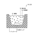
図2は、照明装置11におけるLED13の縦断面図である。図3は、照明装置11においてLED13と発光色の異なる他のLED14の縦断面図である。
図4は、LED13,14の駆動を制御するLED駆動制御部1の構成を示すブロック図である。
以上のように、本実施形態の照明装置11は、異なる発光色のLED13,14が基板12上にそれぞれ列をなして実装された光源部10を備えている。この光源部10において、LED13,14は、それぞれの列の間で、LEDチップ16が列の方向(X方向)と直交する方向(Y方向)に並ぶように配置されている。このように、LED13,14のそれぞれの発光点であるLEDチップ16が列と直交する方向に並ぶので、2つの発光点が近接することにより、LED13,14からのそれぞれの出射光の混色性が向上する。
本発明の実施形態2について、図4~図13および図26~図30を参照して説明する。
図5の(a)は実施形態2に係る照明装置21における光源部20の一部を拡大して示す平面図であり、図5の(b)は照明装置21の縦断面図である。
図6は、照明装置21におけるLED22A(第1LED)の縦断面図である。
図7の(a)は照明装置21における混色状態の一部を拡大して示す正面図であり、図7の(b)は照明装置21の縦断面図である。
次に、他のLED22を採用した光源部20について説明する。
続いて、他のLED22を採用した光源部20について説明する。
さらに、他のLED22を採用した光源部20について説明する。
さらに、他のLED22を採用した光源部20について説明する。
第1の構成に係るLED22Eにおいて、パッケージ23の一方の凹部に形成される第1光源LS1および他方の凹部に形成される第2光源LS2は、樹脂17に同じ蛍光体18,19が分散されている。ただし、第1光源LS1および第2光源LS2は、蛍光体18,19の混合比や混合量が異なることにより、異なる色の光を発する。
図26に示すように、第2の構成に係るLED22Eにおいて、第1の構成に係るLED22Eと異なり、第1光源LS1の樹脂17には蛍光体18A,19が分散され、第2光源LS2の樹脂17には蛍光体18B,19が分散されている。
αSiAlON蛍光体化学式:Ca(Si,Al)12(O,N)16:Eu
例えば、禁制遷移タイプの蛍光体材料として、後述の実施形態8に示す赤色蛍光体の物質を用いてもよい。
図26に示すように、第3の構成に係るLED22Eにおいて、第2の構成に係るLED22Eと同様、第1光源LS1の樹脂17には赤色の蛍光体18Aが分散され、第2光源LS2の樹脂17には赤色の蛍光体18Bが分散されている。ただし、第3の構成に係るLED22Eにおいて、第1光源LS1の樹脂17には緑色の蛍光体19Aが分散され、第2光源LS2の樹脂17には緑色の蛍光体19Bが分散されている。
さらに、他のLED22を採用した光源部20について説明する。
上記の第1の構成に係るLED22Fでは、LEDチップ16Cのピーク波長が415nm以上かつ460nm未満である一方、LEDチップ16Dのピーク波長が460nm以上かつ500nm以下である。
第2の構成に係るLED22Fにおいて、LEDチップ16Cのピーク波長は350nm以上かつ410nm以下(青色光~近紫外光)であり、LEDチップ16Dのピーク波長は445nmを中心とする所定範囲(445nm前後)である。
図29の(a)は実施形態2に係る照明装置21におけるLED22Gを含む(第7LED)他の光源部20Aの一部を拡大して示す平面図である。図29の(b)は照明装置21における他のLED22Gを含む光源部20Bの一部を拡大して示す平面図である。
図29の(a)に示すように、光源部20Aは、第1の構成に係るLED22Gを複数備えている。当該LED22Gは、第1光源LS1に1つのLEDチップ16が実装され、第2光源LS2に複数(図29の(a)では3個)のLEDチップ16が実装されている。第2光源LS2における複数のLEDチップ16は、X方向に並ぶように配置されるとともに、電気的に直列に接続されている。これにより、当該複数のLEDチップ16は、接続数に応じた輝度の光を出射する。
図29の(b)に示すように、光源部20Bは、第2の構成に係るLED22Gを複数備えている。当該LED22Gは、第1光源LS1に1つのLEDチップ16が実装され、第2光源LS2に1つのLEDチップ16Eが実装されている。LEDチップ16Eは、LEDチップ16よりも長辺が長くなるように形成されており、その長さに応じた輝度の光を出射する。
上記のように構成される第1および第2の構成に係るLED22Gでは、第2光源LS2の光量を第1光源LS1の光量よりも大きくすることができる。これにより、第1光源LS1および第2光源LS2の光量を異ならせて光の調色を行う場合などに有効である。
図30は、LED22H(第8LED)の平面図である。
以上に述べた各LED22B~22Hは、いずれも1つのパッケージ23において構成されている。しかしながら、各LED22B~22Hは、実施形態1におけるLED13,14のように、個別の2つのLEDとして構成されてもよい。
本発明の実施形態3について、図4、図14および図15を参照して説明する。
図14の(a)は実施形態3に係る照明装置31における光源部30の一部を拡大して示す平面図であり、図14の(b)は照明装置31の縦断面図である。
図15は、照明装置31におけるLED32の縦断面図である。
以上のように、本実施形態の照明装置31は、同色のLED32が基板12上に2つの列をなして実装された光源部30を備えている。この光源部30において、LED32は、それぞれの列の間で、LEDチップ16が列の方向(X方向)と直交する方向(Y方向)に並ぶように配置されている。このように、LED32のそれぞれの発光点であるLEDチップ16が列と直交する方向に並ぶので、導光板15の光入射部15aの幅方向についての入射光の光量が、図23に示す従来の構成(LED222が一列に配置されている)に比べて2倍に増加する。これにより、導光板15から得られる光強度を増大させることができる。
本発明の実施形態4について、図4、図16および図17を参照して説明する。
図16の(a)は実施形態4に係る照明装置41における光源部40の一部を拡大して示す平面図であり、図16の(b)は照明装置41の縦断面図である。
図17は、照明装置41におけるLED42の縦断面図である。
以上のように、本実施形態の照明装置41は、同じ発光色の光を出射するLED42が基板12上に列をなして実装された光源部40を備えている。この光源部40において、LED42は、2つのLEDチップ16が基板12の長手方向に沿って成すそれぞれの列の間で、LEDチップ16が列の方向(X方向)と直交する方向(Y方向)に並ぶように配置されている。このように、LED42における発光点である2つのLEDチップ16が列と直交する方向に並ぶ。これにより、導光板15の光入射部15aの幅方向についての入射光の光量が、図23に示す従来の構成(LED222が一列に配置されている)に比べて2倍に増加する。これにより、導光板15から得られる光強度を増大させることができる。
本発明の実施形態5について、図4および図18を参照して説明する。
図18の(a)は実施形態5に係る照明装置51における光源部50の一部を拡大して示す平面図であり、図18の(b)は照明装置51の縦断面図である。
LED53は、実施形態2におけるLED22のパッケージ23と異なり3つの凹面部を有しており、それぞれの凹面部の底面にLEDチップ53a,53b,53cが実装されている。また、各凹面部が形成する凹部には、樹脂17と同様の樹脂が充填されているが、樹脂には蛍光体が分散されていない。
以上のように、本実施形態の照明装置51は、異なる発光色の光を出射するLED53が基板52上に列をなして実装された光源部50を備えている。この光源部50において、LED53は、3つのLEDチップ53a,53b,53cが基板52の長手方向に沿って成すそれぞれの列の間で、LEDチップ53a,53b,53cが列の方向(X方向)と直交する方向(Y方向)に並ぶように配置されている。このように、LED53における発光点である3つのLEDチップ53a,53b,53cが列と直交する方向に並ぶ。これにより、3つの発光点が近接するので、LED22からのそれぞれの出射光の混色性が向上する。また、赤、緑および青の3色を混色させることにより、白色光を得ることができる。しかも、図4に示すLED駆動制御部1によって、LED53における3つのLEDチップ53a,53b,53cに与える定電流を制御して、各LEDチップ53a,53b,53cの光強度を調整することによって、任意の中間色を得ることができる。
本発明の実施形態6について、図19を参照して説明する。
本発明の実施形態7について、図20を参照して説明する。
本実施形態では、前述の各実施形態で利用可能な蛍光体について説明する。
本実施形態に係る第1の蛍光体群は、それぞれ赤色蛍光体であって、実施形態1~7の各LEDで用いる赤色の蛍光体18,18Aに利用できる。例えば、前述のLED13,22A~22F,32,42で用いる蛍光体18,18Aに好適に利用できる。特に、第1の赤色蛍光体群は、LED22E(第2および第3の構成)の蛍光体18Aとして必ず用いられる。
AはLi,Na,K,Rb,Cs,NH4およびその組合せから選択され、MはAl,Ga,Inおよびその組合せから選択される。
AはLi,Na,K,Rb,Cs、NH4およびその組合せから選択され、MはAl,Ga,Inおよびその組合せから選択される。
MはAl,Ga,Inおよびその組合せから選択される。
AはLi,Na,K,Rb,Cs,NH4およびその組合せから選択される。
AはLi,Na,K,Rb,Cs,NH4およびその組合せから選択され、MはGe,Si,Sn,Ti,Zrおよびその組合せから選択される。
EはMg,Ca,Sr,Ba,Znおよびその組合せから選択され、MはGe,Si,Sn,Ti,Zrおよびその組合せから選択される。
(8)A3[ZrF7]:Mn4+
AはLi,Na,K,Rb,Cs,NH4およびその組合せから選択される。
本実施形態に係る第2の蛍光体群は、それぞれ赤色蛍光体と緑色蛍光体との組合せであって、実施形態1~7の各LEDで用いる赤色の蛍光体18,18Aおよび緑色の蛍光体19,19Aに利用できる。例えば、前述のLED13,22C,22E,22F,32,42で用いる赤色の蛍光体18,18Aおよび緑色の蛍光体19,19Aに好適に利用できる。
当該2価のユーロピウム賦活酸窒化物緑色系発光蛍光体は、
一般式(A):EuaSibAlcOdNe
で実質的に表される。以下、当該2価のユーロピウム賦活酸窒化物緑色系発光蛍光体を「第1の緑色蛍光体」と称する。
(A-1)Eu:0.05、Si:11.50、Al:0.50、O:0.05、N:15.95
(A-2)Eu:0.10、Si:11.00、Al:1.00、O:0.10、N:15.90
(A-3)Eu:0.30、Si:9.80、Al:2.20、O:0.30、N:15.70
(A-4)Eu:0.15、Si:10.00、Al:2.00、O:0.20、N:15.80
(A-5)Eu:0.01、Si:11.60、Al:0.40、O:0.01、N:15.99
(A-6)Eu:0.005、Si:11.70、Al:0.30、O:0.03、N:15.97
第1の緑色蛍光体は、上記の例に限定されることなく、a、b、c、d、eの値の上記の条件を満たす他の組成比で構成される蛍光体であってもよい。
当該2価のユーロピウム賦活珪酸塩蛍光体は、
一般式(B):2(Ba1-f-gMIfEug)O・SiO2
で実質的に表される。以下、当該2価のユーロピウム賦活珪酸塩蛍光体を「第2の緑色蛍光体」と称する。
(B-1)2(Ba0.70Sr0.26Eu0.04)・SiO2
(B-2)2(Ba0.57Sr0.38Eu0.05)O・SiO2
(B-3)2(Ba0.53Sr0.43Eu0.04)O・SiO2
(B-4)2(Ba0.82Sr0.15Eu0.03)O・SiO2
(B-5)2(Ba0.46Sr0.49Eu0.05)O・SiO2
(B-6)2(Ba0.59Sr0.35Eu0.06)O・SiO2
(B-7)2(Ba0.52Sr0.40Eu0.08)O・SiO2
(B-8)2(Ba0.85Sr0.10Eu0.05)O・SiO2
(B-9)2(Ba0.47Sr0.50Eu0.03)O・SiO2
(B-10)2(Ba0.54Sr0.36Eu0.10)O・SiO2
(B-11)2(Ba0.69Sr0.25Ca0.02Eu0.04)O・SiO2
(B-12)2(Ba0.56Sr0.38Mg0.01Eu0.05)O・SiO2
(B-13)2(Ba0.81Sr0.13Mg0.01Ca0.01Eu0.04)O・SiO2
第2の緑色蛍光体は、上記の例に限定されることなく、MIの他の組合せおよびf、gの値の上記の条件を満たす他の組成比で構成される蛍光体であってもよい。
当該4価のマンガン賦活フッ化4価金属塩蛍光体は、
一般式(C):MII2(MIII1-hMnh)F6
で実質的に表される。以下、当該4価のマンガン賦活フッ化4価金属塩蛍光体を「第1の赤色蛍光体」と称する。
(C-1)K2(Ti0.99Mn0.01)F6
(C-2)K2(Ti0.9Mn0.1)F6
(C-3)K2(Ti0.999Mn0.001)F6
(C-4)Na2(Zr0.98Mn0.02)F6
(C-5)Cs2(Si0.95Mn0.05)F6
(C-6)Cs2(Sn0.98Mn0.02)F6
(C-7)K2(Ti0.88Zr0.10Mn0.02)F6
(C-8)Na2(Ti0.75Sn0.20Mn0.05)F6
(C-9)Cs2(Ge0.999Mn0.001)F6、
(C-10)(K0.80Na0.20)2(Ti0.69Ge0.30Mn0.01)F6
第1の赤色蛍光体は、上記の例に限定されることなく、MIIおよびMIIIの他の組合せおよびhの値の上記の条件を満たす他の組成比で構成される蛍光体であってもよい。
当該4価のマンガン賦活フッ化4価金属塩蛍光体は、
一般式(D):MIV(MIII1-hMnh)F6
で実質的に表される。以下、当該4価のマンガン賦活フッ化4価金属塩蛍光体を「第2の赤色系発光蛍光体」と称する。
(D-1)Zn(Ti0.98Mn0.02)F6
(D-2)Ba(Zr0.995Mn0.005)F6
(D-3)Ca(Ti0.995Mn0.005)F6
(D-4)Sr(Zr0.98Mn0.02)F6
第2の赤色蛍光体は、上記の例に限定されることなく、MIIIおよびMIVの他の組合せおよびhの値の上記の条件を満たす他の組成比で構成される蛍光体であってもよい。
実施形態1~7で用いる各LEDチップの外観については、上面側(Z方向の反対方向)から見た各LEDチップの形状が長方形であることが望ましい。また、各LEDチップの長手方向と基板12,52の長手方向とが同じ方向(X方向)であるように、各LEDチップが基板12,52に配置されていることが望ましい。
本発明の態様1に係る照明装置(11,21,31,41,51)は、導光板(15,54)と、基板(12,52)および当該基板上に配置された複数のLEDチップ(16,25)を有し、前記LEDチップの出射光が前記導光板の光入射部に入射されるように配置される光源部(10,20,30,40,50)とを備え、前記LEDチップが、前記基板上に複数の列を形成するように配置されるとともに、各列の間で前記列と直交する方向に並ぶように配置されている。
タによる色分離が向上するので、緑色の色域を拡大することができる。さらに、緑色蛍光体として、1~5nmほど短い発光波長を有する蛍光体を選択することで、青色、緑色および赤色の全体の色域を拡大させることも可能である。
10 光源部
11 照明装置
12 基板
13 LED
14 LED
15 導光板
15a 光入射部
16 LEDチップ
16A LEDチップ
16B LEDチップ(青色LEDチップ)
18 蛍光体(赤色蛍光体)
19 蛍光体(緑色蛍光体)
20 光源部
21 照明装置
22 LED
22A LED
22B LED
22C LED
22D LED
22E LED
22F LED
22G LED
22H LED
23 パッケージ
23c 隔壁
24 蛍光体(緑色蛍光体)
25 LEDチップ(緑色LEDチップ)
31 照明装置
32 LED
41 照明装置
42 LED
50 光源部
51 照明装置
52 基板
53 LED
54 導光板
54a 光入射部
101 液晶表示装置(表示装置)
103 バックライト(照明装置)
103a 導光板
103b 基板
103c LED
111 シーリングライト(照明器具)
112 照明装置
112a 導光板
112b 基板
112c LED
LS1 第1光源
LS2 第2光源
V0 黒体輻射軌跡
S 領域
V1 等偏差線(第1等偏差線)
V2 等偏差線(第2等偏差線)
W1 等色温度線(第1等色温度線)
W2 等色温度線(第21等色温度線)
Claims (18)
- 導光板と、
基板および当該基板上に配置された複数のLEDチップを有し、前記LEDチップの出射光が前記導光板の光入射部に入射されるように配置される光源部とを備え、
前記LEDチップは、前記基板上に複数の列を形成するように配置されるとともに、各列の間で前記列と直交する方向に並ぶように配置されていることを特徴とする照明装置。 - 前記光源部は、各列の間で隣接する2つの前記LEDチップを収納する単一のパッケージをさらに有していることを特徴とする請求項1に記載の照明装置。
- 前記LEDチップは、互いに光学的に分離され、発光色が同一であることを特徴とする請求項1または2に記載の照明装置。
- 前記LEDチップは、蛍光体と組み合わされることにより白色光を発するLEDを構成することを特徴とする請求項3に記載の照明装置。
- 各列間で隣接する前記LEDチップは、前記列毎に異なる蛍光体と組み合わされていることを特徴とする請求項1から3のいずれか1項に記載の照明装置。
- 前記LEDチップと前記蛍光体との組み合わせは、黒体輻射曲線上の2点の色度の光を発することを特徴とする請求項5に記載の照明装置。
- 前記LEDチップが2列に配置され、
各列間で隣接する前記LEDチップは青色LEDチップであり、一方の前記LEDチップが赤色蛍光体と組み合わされ、他方の前記LEDチップが緑色蛍光体と組み合わされることを特徴とする請求項5に記載の照明装置。 - 各列間で隣接する前記LEDチップの一方は、前記赤色蛍光体の最適励起波長に適合するピーク波長を有し、前記LEDチップの他方は、前記緑色蛍光体の最適励起波長に適合するピーク波長を有することを特徴とする請求項7に記載の照明装置。
- 前記LEDチップが2列に配置され、
各列間で隣接する前記LEDチップの一方は緑色LEDチップであり、他方は青色LEDチップであり、
前記青色LEDチップは赤色蛍光体と組み合わされることを特徴とする請求項1または2に記載の照明装置。 - 前記LEDチップが2列に配置され、
前記LEDチップは、青色LEDチップであり、かつ赤色蛍光体および緑色蛍光体と組み合わされており、
各列間で隣接する2つの前記LEDチップと、赤色蛍光体および緑色蛍光体との組合せが、それぞれ第1光源および第2光源を形成し、
前記第1光源は、色温度が2400Kである電球色から色温度が7000Kである昼光色までのいずれかの色度を有する白色光を発し、
前記第2光源は、xy色度図上の点A(0.555,0.394)および点B(0.419,0.343)に対し、前記点Aを通る、第1等色温度線および黒体輻射軌跡に対する第1等偏差線と、前記点B(0.419,0.343)を通る、第2等色温度線および前記黒体輻射軌跡に対する第2等偏差線とで囲まれる領域内の色度を有する光を発することを特徴とする請求項1から3のいずれか1項に記載の照明装置。 - 前記LEDチップは、2列に配置され、かつ青色LEDチップであり、
各列間で隣接する2つの前記LEDチップのうち、一方の前記LEDチップが、415nm以上かつ460nm未満のピーク波長を有し、かつ赤色蛍光体および緑色蛍光体と組み合わされ、
他方の前記LEDチップが、460nm以上かつ500nm以下のピーク波長を有し、かつ蛍光体と組み合わされないことを特徴とする請求項1から3のいずれか1項に記載の照明装置。 - 前記LEDチップは、2列に配置され、かつ青色LEDチップであり、
各列間で隣接する2つの前記LEDチップのうち、一方の前記LEDチップが、350nm以上かつ410nm以下のピーク波長を有し、かつ赤色蛍光体および緑色蛍光体と組み合わされ、
他方の前記LEDチップが、蛍光体と組み合わされないことを特徴とする請求項1から3のいずれか1項に記載の照明装置。 - 前記LEDチップが2列に配置され、
前記LEDチップは、青色LEDチップであり、かつ赤色蛍光体および緑色蛍光体と組み合わされており、
各列間で隣接する2つの前記LEDチップと、赤色蛍光体および緑色蛍光体との組合せが、それぞれ第1光源および第2光源を形成し、
前記第1光源は、赤色蛍光体として禁制遷移タイプの蛍光体材料を含み、
前記第2光源は、赤色蛍光体として許容遷移タイプの蛍光体材料を含むことを特徴とする請求項1から3のいずれか1項に記載の照明装置。 - 前記LEDチップが2列に配置され、
前記LEDチップは、青色LEDチップであり、かつ赤色蛍光体および緑色蛍光体と組み合わされており、
各列間で隣接する2つの前記LEDチップと、赤色蛍光体および緑色蛍光体との組合せが、それぞれ第1光源および第2光源を形成し、
前記第1光源は、赤色蛍光体および緑色蛍光体として禁制遷移タイプの蛍光体材料を含み、
前記第2光源は、赤色蛍光体および緑色蛍光体として許容遷移タイプの蛍光体材料を含むことを特徴とする請求項1から3のいずれか1項に記載の照明装置。 - 前記LEDチップがパッケージの内部に封止されることによりLEDが形成され、当該LEDが前記基板上に実装されており、
前記LEDの発光面が長方形を成し、該発光面の長手方向と該基板の長手方向とが同じ方向であることを特徴とする請求項1または2に記載の照明装置。 - 前記LEDチップは、各列の間で前記列と直交する方向に3個並ぶことを特徴とする請求項1から3のいずれか1項に記載の照明装置。
- 請求項1から16のいずれか1項に記載の照明装置を備える照明機器。
- 請求項1から16のいずれか1項に記載の照明装置をバックライトとして備える表示装置。
Priority Applications (2)
| Application Number | Priority Date | Filing Date | Title |
|---|---|---|---|
| US14/783,527 US10018776B2 (en) | 2013-04-15 | 2014-04-10 | Illumination device, illumination equipment, and display device |
| JP2015512460A JP6262211B2 (ja) | 2013-04-15 | 2014-04-10 | 照明装置、照明機器および表示装置 |
Applications Claiming Priority (4)
| Application Number | Priority Date | Filing Date | Title |
|---|---|---|---|
| JP2013085294 | 2013-04-15 | ||
| JP2013-085294 | 2013-04-15 | ||
| JP2013-238220 | 2013-11-18 | ||
| JP2013238220 | 2013-11-18 |
Publications (1)
| Publication Number | Publication Date |
|---|---|
| WO2014171394A1 true WO2014171394A1 (ja) | 2014-10-23 |
Family
ID=51731337
Family Applications (1)
| Application Number | Title | Priority Date | Filing Date |
|---|---|---|---|
| PCT/JP2014/060413 Ceased WO2014171394A1 (ja) | 2013-04-15 | 2014-04-10 | 照明装置、照明機器および表示装置 |
Country Status (3)
| Country | Link |
|---|---|
| US (1) | US10018776B2 (ja) |
| JP (1) | JP6262211B2 (ja) |
| WO (1) | WO2014171394A1 (ja) |
Cited By (17)
| Publication number | Priority date | Publication date | Assignee | Title |
|---|---|---|---|---|
| JP2016115941A (ja) * | 2014-12-16 | 2016-06-23 | シチズン電子株式会社 | 発光装置 |
| CN105938707A (zh) * | 2015-03-06 | 2016-09-14 | 三星显示有限公司 | 显示装置 |
| JP2017034148A (ja) * | 2015-08-04 | 2017-02-09 | 日亜化学工業株式会社 | 発光装置および発光装置を備えたバックライト |
| KR20170026884A (ko) * | 2015-08-31 | 2017-03-09 | 엘지디스플레이 주식회사 | 백라이트 유닛 및 이를 포함하는 액정표시장치 |
| KR20170026883A (ko) * | 2015-08-31 | 2017-03-09 | 엘지디스플레이 주식회사 | 발광다이오드 램프 및 이를 포함하는 액정표시장치 |
| JP2017076093A (ja) * | 2015-10-16 | 2017-04-20 | 株式会社デンソー | 液晶表示装置 |
| CN106784172A (zh) * | 2015-11-23 | 2017-05-31 | 东贝光电科技股份有限公司 | Led发光装置的制造方法及led发光装置 |
| KR20170078783A (ko) * | 2014-10-31 | 2017-07-07 | 코닌클리케 필립스 엔.브이. | 온도 안정성 선속 및 포화 적색 색점을 갖는 인광체 변환형 led |
| US9704834B2 (en) | 2013-05-28 | 2017-07-11 | Sharp Kabushiki Kaisha | Method for manufacturing light-emitting device |
| JP2019029584A (ja) * | 2017-08-02 | 2019-02-21 | シャープ株式会社 | 発光装置及び画像表示装置 |
| JP2019134047A (ja) * | 2018-01-31 | 2019-08-08 | 日亜化学工業株式会社 | 発光装置及び光源 |
| JPWO2018159569A1 (ja) * | 2017-02-28 | 2019-12-19 | 東洋紡株式会社 | 液晶表示装置 |
| JPWO2018159568A1 (ja) * | 2017-02-28 | 2019-12-19 | 東洋紡株式会社 | 液晶表示装置 |
| JP2020030224A (ja) * | 2018-08-08 | 2020-02-27 | セイコーエプソン株式会社 | 波長変換素子、光源装置およびプロジェクター |
| KR20200045568A (ko) * | 2017-09-20 | 2020-05-04 | 제네럴 일렉트릭 컴퍼니 | 녹색 형광체들 및 그것의 디바이스들 |
| JP2021103319A (ja) * | 2015-10-16 | 2021-07-15 | 東洋紡株式会社 | 液晶表示装置及び偏光板 |
| US11493679B2 (en) * | 2020-02-13 | 2022-11-08 | Samsung Display Co., Ltd. | Backlight unit and display device including the same |
Families Citing this family (32)
| Publication number | Priority date | Publication date | Assignee | Title |
|---|---|---|---|---|
| WO2015068513A1 (ja) * | 2013-11-08 | 2015-05-14 | シャープ株式会社 | 発光装置、及び照明装置 |
| US20150345724A1 (en) * | 2014-04-02 | 2015-12-03 | Abl Ip Holding Llc | Composite light source systems and methods |
| US10194503B2 (en) | 2014-04-02 | 2019-01-29 | Abl Ip Holding Llc | Composite light source systems and methods |
| DE102014108004A1 (de) * | 2014-06-06 | 2015-12-17 | Osram Opto Semiconductors Gmbh | Verfahren zum Herstellen eines optoelektronischen Bauelements und optoelektronisches Bauelement |
| CN104110614A (zh) * | 2014-07-08 | 2014-10-22 | 北京京东方视讯科技有限公司 | 一种白光led光源、背光模组及显示装置 |
| JP2017073412A (ja) * | 2015-10-05 | 2017-04-13 | 株式会社ジャパンディスプレイ | 表示装置及び光源装置 |
| CN105700235A (zh) * | 2016-04-13 | 2016-06-22 | 京东方科技集团股份有限公司 | 一种背光模组及显示装置 |
| US20170307190A1 (en) * | 2016-04-21 | 2017-10-26 | Abl Ip Holding Llc | Luminaires with multiple illumination panels |
| CA2976195C (en) * | 2016-08-11 | 2021-04-13 | Abl Ip Holding Llc | Luminaires with transition zones for glare control |
| KR20180032063A (ko) * | 2016-09-21 | 2018-03-29 | 서울반도체 주식회사 | 발광 다이오드 패키지 및 발광 다이오드 모듈 |
| US10193018B2 (en) * | 2016-12-29 | 2019-01-29 | Intel Corporation | Compact low power head-mounted display with light emitting diodes that exhibit a desired beam angle |
| US10955607B2 (en) * | 2017-03-07 | 2021-03-23 | Lumileds Llc | LED lighting device with remote phosphor in-coupling structure for in-coupling light from light emitting diodes |
| KR102487411B1 (ko) * | 2017-10-31 | 2023-01-12 | 엘지디스플레이 주식회사 | 발광소자 패키지 및 전자기기 |
| CN207720473U (zh) * | 2017-12-15 | 2018-08-10 | 漳州立达信灯具有限公司 | 多档色温切换led电路 |
| JP7064129B2 (ja) * | 2017-12-22 | 2022-05-10 | 日亜化学工業株式会社 | 発光装置 |
| CN108458323B (zh) * | 2018-02-14 | 2020-01-17 | 易事化控制设备股份有限公司 | 一种降低蓝光危害的led灯珠荧光粉、led灯珠及其制备方法 |
| KR20190108216A (ko) * | 2018-03-13 | 2019-09-24 | 삼성디스플레이 주식회사 | 표시 장치 및 이의 구동 방법 |
| KR102756868B1 (ko) * | 2019-08-27 | 2025-01-20 | 주식회사 루멘스 | 엘이디 백라이트 유닛을 이용하는 디스플레이 장치 |
| US20200124786A1 (en) * | 2018-10-18 | 2020-04-23 | Lumens Co., Ltd. | Display devices using led backlight units and led packages for the backlight units |
| KR102669275B1 (ko) * | 2018-11-12 | 2024-05-24 | 쑤저우 레킨 세미컨덕터 컴퍼니 리미티드 | 발광소자 패키지 |
| CN109343271A (zh) * | 2018-11-13 | 2019-02-15 | 惠州市华星光电技术有限公司 | 背光模组及液晶显示器 |
| CN111341765A (zh) * | 2018-12-18 | 2020-06-26 | 深圳Tcl新技术有限公司 | 一种背光模组 |
| EP3931634A4 (en) * | 2019-02-25 | 2023-03-15 | Visteon Global Technologies, Inc. | DISPLAY SYSTEM |
| KR102872842B1 (ko) * | 2019-03-22 | 2025-10-22 | 삼성전자주식회사 | 백색 발광 모듈 |
| KR102620075B1 (ko) * | 2019-04-29 | 2024-01-03 | 삼성전자주식회사 | 색 온도 조절이 가능한 디스플레이 패널 및 디스플레이 장치 |
| CN212115725U (zh) * | 2019-11-11 | 2020-12-08 | 漳州立达信光电子科技有限公司 | Led灯色温控制电路及led灯具 |
| US10962829B1 (en) * | 2020-03-31 | 2021-03-30 | Chongqing Boe Optoelectronics Technology Co., Ltd. | Light bar, backlight module and display device |
| WO2021204650A1 (de) * | 2020-04-09 | 2021-10-14 | Osram Opto Semiconductors Gmbh | Strahlungsemittierendes bauelement, lichtquelle und display-vorrichtung |
| CN117897655A (zh) * | 2022-06-29 | 2024-04-16 | 京东方科技集团股份有限公司 | 背光模组及显示装置 |
| KR20240031788A (ko) | 2022-09-01 | 2024-03-08 | 삼성전자주식회사 | 디스플레이용 발광 소자 및 이를 포함하는 백라이트 유닛 |
| TWI883532B (zh) * | 2023-09-07 | 2025-05-11 | 元太科技工業股份有限公司 | 顯示裝置與其光學模組 |
| CN119713161A (zh) * | 2024-06-03 | 2025-03-28 | 普瑞光电(厦门)股份有限公司 | 可实现高品质可调白光的发光装置 |
Citations (7)
| Publication number | Priority date | Publication date | Assignee | Title |
|---|---|---|---|---|
| JP2004342472A (ja) * | 2003-05-16 | 2004-12-02 | Advanced Display Inc | 面状光源装置及びそれを用いた表示装置 |
| JP2006073656A (ja) * | 2004-08-31 | 2006-03-16 | Nichia Chem Ind Ltd | 発光装置 |
| JP2007122950A (ja) * | 2005-10-26 | 2007-05-17 | Fujikura Ltd | 照明装置 |
| JP2007287692A (ja) * | 2006-04-17 | 2007-11-01 | Samsung Electro-Mechanics Co Ltd | エッジ型バックライトユニット |
| WO2009145298A1 (ja) * | 2008-05-30 | 2009-12-03 | シャープ株式会社 | 発光装置、面光源、液晶表示装置および発光装置の製造方法 |
| JP2011228538A (ja) * | 2010-04-21 | 2011-11-10 | Panasonic Electric Works Co Ltd | 発光装置及びそれを用いる照明装置 |
| JP2012028339A (ja) * | 2011-09-30 | 2012-02-09 | Sharp Corp | 照明装置 |
Family Cites Families (16)
| Publication number | Priority date | Publication date | Assignee | Title |
|---|---|---|---|---|
| JP4654670B2 (ja) | 2003-12-16 | 2011-03-23 | 日亜化学工業株式会社 | 発光装置及びその製造方法 |
| US7553060B2 (en) | 2004-09-10 | 2009-06-30 | Sharp Kabushiki Kaisha | Backlight device and liquid crystal display |
| JP2007049114A (ja) | 2005-05-30 | 2007-02-22 | Sharp Corp | 発光装置とその製造方法 |
| US8210732B2 (en) | 2006-06-16 | 2012-07-03 | Fujifilm Corporation | Light guide plate, light guide plate assembly, and planar lighting device and liquid crystal display device using these |
| JP4813982B2 (ja) | 2006-06-16 | 2011-11-09 | 富士フイルム株式会社 | 導光板組立体およびこれを用いる面状照明装置 |
| JP5263722B2 (ja) | 2007-06-08 | 2013-08-14 | シャープ株式会社 | 蛍光体、発光装置および画像表示装置 |
| JP5220381B2 (ja) | 2007-10-16 | 2013-06-26 | ミネベア株式会社 | 面状照明装置 |
| JP4906771B2 (ja) | 2008-03-31 | 2012-03-28 | 富士フイルム株式会社 | 面状照明装置及びそれを用いる液晶表示装置 |
| JP5236366B2 (ja) | 2008-07-01 | 2013-07-17 | ミネベア株式会社 | 線状光源装置、および面状照明装置 |
| JP5005712B2 (ja) * | 2009-02-03 | 2012-08-22 | 三菱電機株式会社 | 発光装置 |
| JP2012186070A (ja) | 2011-03-07 | 2012-09-27 | Toshiba Lighting & Technology Corp | 照明器具 |
| WO2012124509A1 (ja) | 2011-03-11 | 2012-09-20 | シャープ株式会社 | 光源、照明装置及び表示装置 |
| JP5830678B2 (ja) * | 2011-06-23 | 2015-12-09 | パナソニックIpマネジメント株式会社 | 照明装置および照明器具 |
| WO2013125521A1 (ja) | 2012-02-20 | 2013-08-29 | シャープ株式会社 | 照明装置 |
| JP2013171686A (ja) | 2012-02-20 | 2013-09-02 | Sharp Corp | 照明装置 |
| JP2013171687A (ja) | 2012-02-20 | 2013-09-02 | Sharp Corp | 照明装置 |
-
2014
- 2014-04-10 WO PCT/JP2014/060413 patent/WO2014171394A1/ja not_active Ceased
- 2014-04-10 JP JP2015512460A patent/JP6262211B2/ja not_active Expired - Fee Related
- 2014-04-10 US US14/783,527 patent/US10018776B2/en not_active Expired - Fee Related
Patent Citations (7)
| Publication number | Priority date | Publication date | Assignee | Title |
|---|---|---|---|---|
| JP2004342472A (ja) * | 2003-05-16 | 2004-12-02 | Advanced Display Inc | 面状光源装置及びそれを用いた表示装置 |
| JP2006073656A (ja) * | 2004-08-31 | 2006-03-16 | Nichia Chem Ind Ltd | 発光装置 |
| JP2007122950A (ja) * | 2005-10-26 | 2007-05-17 | Fujikura Ltd | 照明装置 |
| JP2007287692A (ja) * | 2006-04-17 | 2007-11-01 | Samsung Electro-Mechanics Co Ltd | エッジ型バックライトユニット |
| WO2009145298A1 (ja) * | 2008-05-30 | 2009-12-03 | シャープ株式会社 | 発光装置、面光源、液晶表示装置および発光装置の製造方法 |
| JP2011228538A (ja) * | 2010-04-21 | 2011-11-10 | Panasonic Electric Works Co Ltd | 発光装置及びそれを用いる照明装置 |
| JP2012028339A (ja) * | 2011-09-30 | 2012-02-09 | Sharp Corp | 照明装置 |
Cited By (38)
| Publication number | Priority date | Publication date | Assignee | Title |
|---|---|---|---|---|
| US9704834B2 (en) | 2013-05-28 | 2017-07-11 | Sharp Kabushiki Kaisha | Method for manufacturing light-emitting device |
| KR20170078783A (ko) * | 2014-10-31 | 2017-07-07 | 코닌클리케 필립스 엔.브이. | 온도 안정성 선속 및 포화 적색 색점을 갖는 인광체 변환형 led |
| KR102396732B1 (ko) | 2014-10-31 | 2022-05-12 | 루미리즈 홀딩 비.브이. | 온도 안정성 선속 및 포화 적색 색점을 갖는 인광체 변환형 led |
| JP2017536694A (ja) * | 2014-10-31 | 2017-12-07 | コーニンクレッカ フィリップス エヌ ヴェKoninklijke Philips N.V. | 温度安定フラックスと飽和赤色ポイントを用いた蛍光変換led |
| JP2022079746A (ja) * | 2014-12-16 | 2022-05-26 | シチズン電子株式会社 | 発光装置 |
| JP2016115941A (ja) * | 2014-12-16 | 2016-06-23 | シチズン電子株式会社 | 発光装置 |
| US11756939B2 (en) | 2014-12-16 | 2023-09-12 | Citizen Electronics Co., Ltd. | Light emitting element with particular phosphors |
| US11342312B2 (en) | 2014-12-16 | 2022-05-24 | Citizen Electronics Co., Ltd. | Light emitting element with particular phosphors |
| KR102275027B1 (ko) * | 2015-03-06 | 2021-07-12 | 삼성디스플레이 주식회사 | 표시 장치 및 이의 구동 방법 |
| CN105938707A (zh) * | 2015-03-06 | 2016-09-14 | 三星显示有限公司 | 显示装置 |
| KR20160108783A (ko) * | 2015-03-06 | 2016-09-20 | 삼성디스플레이 주식회사 | 표시 장치 및 이의 구동 방법 |
| US11398460B2 (en) | 2015-08-04 | 2022-07-26 | Nichia Corporation | Light-emitting device and backlight including light-emitting device |
| US10971481B2 (en) | 2015-08-04 | 2021-04-06 | Nichia Corporation | Light-emitting device and backlight including light-emitting device |
| JP2017034148A (ja) * | 2015-08-04 | 2017-02-09 | 日亜化学工業株式会社 | 発光装置および発光装置を備えたバックライト |
| US10529695B2 (en) | 2015-08-04 | 2020-01-07 | Nichia Corporation | Light-emitting device and backlight including light-emitting device |
| KR20170026884A (ko) * | 2015-08-31 | 2017-03-09 | 엘지디스플레이 주식회사 | 백라이트 유닛 및 이를 포함하는 액정표시장치 |
| KR102297988B1 (ko) * | 2015-08-31 | 2021-09-03 | 엘지디스플레이 주식회사 | 발광다이오드 램프 및 이를 포함하는 액정표시장치 |
| KR20170026883A (ko) * | 2015-08-31 | 2017-03-09 | 엘지디스플레이 주식회사 | 발광다이오드 램프 및 이를 포함하는 액정표시장치 |
| KR102272351B1 (ko) * | 2015-08-31 | 2021-07-02 | 엘지디스플레이 주식회사 | 백라이트 유닛 및 이를 포함하는 액정표시장치 |
| JP7160127B2 (ja) | 2015-10-16 | 2022-10-25 | 東洋紡株式会社 | 液晶表示装置及び偏光板 |
| JP7347615B2 (ja) | 2015-10-16 | 2023-09-20 | 東洋紡株式会社 | 液晶表示装置及び偏光板 |
| JP2021103319A (ja) * | 2015-10-16 | 2021-07-15 | 東洋紡株式会社 | 液晶表示装置及び偏光板 |
| JP2017076093A (ja) * | 2015-10-16 | 2017-04-20 | 株式会社デンソー | 液晶表示装置 |
| JP2022173328A (ja) * | 2015-10-16 | 2022-11-18 | 東洋紡株式会社 | 液晶表示装置及び偏光板 |
| CN106784172A (zh) * | 2015-11-23 | 2017-05-31 | 东贝光电科技股份有限公司 | Led发光装置的制造方法及led发光装置 |
| JP7184033B2 (ja) | 2017-02-28 | 2022-12-06 | 東洋紡株式会社 | 液晶表示装置 |
| JPWO2018159569A1 (ja) * | 2017-02-28 | 2019-12-19 | 東洋紡株式会社 | 液晶表示装置 |
| JP7070539B2 (ja) | 2017-02-28 | 2022-05-18 | 東洋紡株式会社 | 液晶表示装置 |
| JPWO2018159568A1 (ja) * | 2017-02-28 | 2019-12-19 | 東洋紡株式会社 | 液晶表示装置 |
| JP2019029584A (ja) * | 2017-08-02 | 2019-02-21 | シャープ株式会社 | 発光装置及び画像表示装置 |
| JP2020534694A (ja) * | 2017-09-20 | 2020-11-26 | ゼネラル・エレクトリック・カンパニイ | 緑色発光蛍光体およびそのデバイス |
| JP7257391B2 (ja) | 2017-09-20 | 2023-04-13 | ゼネラル・エレクトリック・カンパニイ | 緑色発光蛍光体およびそのデバイス |
| KR20200045568A (ko) * | 2017-09-20 | 2020-05-04 | 제네럴 일렉트릭 컴퍼니 | 녹색 형광체들 및 그것의 디바이스들 |
| KR102671144B1 (ko) * | 2017-09-20 | 2024-05-30 | 제네럴 일렉트릭 컴퍼니 | 녹색 형광체들 및 그것의 디바이스들 |
| JP2019134047A (ja) * | 2018-01-31 | 2019-08-08 | 日亜化学工業株式会社 | 発光装置及び光源 |
| JP7187879B2 (ja) | 2018-08-08 | 2022-12-13 | セイコーエプソン株式会社 | 波長変換素子、光源装置およびプロジェクター |
| JP2020030224A (ja) * | 2018-08-08 | 2020-02-27 | セイコーエプソン株式会社 | 波長変換素子、光源装置およびプロジェクター |
| US11493679B2 (en) * | 2020-02-13 | 2022-11-08 | Samsung Display Co., Ltd. | Backlight unit and display device including the same |
Also Published As
| Publication number | Publication date |
|---|---|
| JP6262211B2 (ja) | 2018-01-17 |
| US20160062023A1 (en) | 2016-03-03 |
| US10018776B2 (en) | 2018-07-10 |
| JPWO2014171394A1 (ja) | 2017-02-23 |
Similar Documents
| Publication | Publication Date | Title |
|---|---|---|
| JP6262211B2 (ja) | 照明装置、照明機器および表示装置 | |
| US10396254B2 (en) | Light emitting device that emits secondary light with a fast response | |
| US9476568B2 (en) | White light illumination system with narrow band green phosphor and multiple-wavelength excitation | |
| KR100946015B1 (ko) | 백색 발광장치 및 이를 이용한 lcd 백라이트용 광원모듈 | |
| JP5005712B2 (ja) | 発光装置 | |
| JP2008140704A (ja) | Ledバックライト | |
| JP2010080935A (ja) | 半導体発光装置及びこれを用いたバックライト光源、バックライト光源システム、表示装置、電子機器 | |
| US20110211336A1 (en) | Light emitting device, and illumination light source, display unit and electronic apparatus including the light emitting device | |
| US20060285324A1 (en) | Color-mixing lighting system | |
| JP5732059B2 (ja) | Led電球 | |
| JP5398657B2 (ja) | 発光デバイス | |
| WO2012035714A1 (ja) | Led電球 | |
| KR20070068709A (ko) | 백색 발광 장치 | |
| CN107466428A (zh) | 光源装置及发光装置 | |
| JP2012191225A (ja) | 発光装置 | |
| JP2010087267A (ja) | Led発光装置 | |
| US10770629B2 (en) | Light emitting device | |
| JP2017152566A (ja) | 発光装置、バックライト、表示装置 | |
| JP2014150293A (ja) | 発光装置 | |
| JP3118485U (ja) | 白色光発光装置 | |
| KR100665221B1 (ko) | 백색 발광 장치 | |
| KR100616689B1 (ko) | 백색 발광 장치 |
Legal Events
| Date | Code | Title | Description |
|---|---|---|---|
| 121 | Ep: the epo has been informed by wipo that ep was designated in this application |
Ref document number: 14785025 Country of ref document: EP Kind code of ref document: A1 |
|
| ENP | Entry into the national phase |
Ref document number: 2015512460 Country of ref document: JP Kind code of ref document: A |
|
| WWE | Wipo information: entry into national phase |
Ref document number: 14783527 Country of ref document: US |
|
| NENP | Non-entry into the national phase |
Ref country code: DE |
|
| 122 | Ep: pct application non-entry in european phase |
Ref document number: 14785025 Country of ref document: EP Kind code of ref document: A1 |