WO2014171248A1 - 殺菌装置 - Google Patents
殺菌装置 Download PDFInfo
- Publication number
- WO2014171248A1 WO2014171248A1 PCT/JP2014/057226 JP2014057226W WO2014171248A1 WO 2014171248 A1 WO2014171248 A1 WO 2014171248A1 JP 2014057226 W JP2014057226 W JP 2014057226W WO 2014171248 A1 WO2014171248 A1 WO 2014171248A1
- Authority
- WO
- WIPO (PCT)
- Prior art keywords
- fluid
- discharge electrode
- conductor
- sterilizer
- ceramic layer
- Prior art date
- Legal status (The legal status is an assumption and is not a legal conclusion. Google has not performed a legal analysis and makes no representation as to the accuracy of the status listed.)
- Ceased
Links
Images

Classifications
-
- A—HUMAN NECESSITIES
- A61—MEDICAL OR VETERINARY SCIENCE; HYGIENE
- A61L—METHODS OR APPARATUS FOR STERILISING MATERIALS OR OBJECTS IN GENERAL; DISINFECTION, STERILISATION OR DEODORISATION OF AIR; CHEMICAL ASPECTS OF BANDAGES, DRESSINGS, ABSORBENT PADS OR SURGICAL ARTICLES; MATERIALS FOR BANDAGES, DRESSINGS, ABSORBENT PADS OR SURGICAL ARTICLES
- A61L9/00—Disinfection, sterilisation or deodorisation of air
-
- H—ELECTRICITY
- H05—ELECTRIC TECHNIQUES NOT OTHERWISE PROVIDED FOR
- H05H—PLASMA TECHNIQUE; PRODUCTION OF ACCELERATED ELECTRICALLY-CHARGED PARTICLES OR OF NEUTRONS; PRODUCTION OR ACCELERATION OF NEUTRAL MOLECULAR OR ATOMIC BEAMS
- H05H1/00—Generating plasma; Handling plasma
- H05H1/24—Generating plasma
- H05H1/2406—Generating plasma using dielectric barrier discharges, i.e. with a dielectric interposed between the electrodes
-
- A—HUMAN NECESSITIES
- A61—MEDICAL OR VETERINARY SCIENCE; HYGIENE
- A61L—METHODS OR APPARATUS FOR STERILISING MATERIALS OR OBJECTS IN GENERAL; DISINFECTION, STERILISATION OR DEODORISATION OF AIR; CHEMICAL ASPECTS OF BANDAGES, DRESSINGS, ABSORBENT PADS OR SURGICAL ARTICLES; MATERIALS FOR BANDAGES, DRESSINGS, ABSORBENT PADS OR SURGICAL ARTICLES
- A61L2/00—Disinfection or sterilisation of materials or objects, in general; Accessories therefor
-
- H—ELECTRICITY
- H05—ELECTRIC TECHNIQUES NOT OTHERWISE PROVIDED FOR
- H05H—PLASMA TECHNIQUE; PRODUCTION OF ACCELERATED ELECTRICALLY-CHARGED PARTICLES OR OF NEUTRONS; PRODUCTION OR ACCELERATION OF NEUTRAL MOLECULAR OR ATOMIC BEAMS
- H05H1/00—Generating plasma; Handling plasma
- H05H1/24—Generating plasma
- H05H1/2406—Generating plasma using dielectric barrier discharges, i.e. with a dielectric interposed between the electrodes
- H05H1/2418—Generating plasma using dielectric barrier discharges, i.e. with a dielectric interposed between the electrodes the electrodes being embedded in the dielectric
-
- H—ELECTRICITY
- H05—ELECTRIC TECHNIQUES NOT OTHERWISE PROVIDED FOR
- H05H—PLASMA TECHNIQUE; PRODUCTION OF ACCELERATED ELECTRICALLY-CHARGED PARTICLES OR OF NEUTRONS; PRODUCTION OR ACCELERATION OF NEUTRAL MOLECULAR OR ATOMIC BEAMS
- H05H1/00—Generating plasma; Handling plasma
- H05H1/24—Generating plasma
- H05H1/2406—Generating plasma using dielectric barrier discharges, i.e. with a dielectric interposed between the electrodes
- H05H1/2437—Multilayer systems
-
- H—ELECTRICITY
- H05—ELECTRIC TECHNIQUES NOT OTHERWISE PROVIDED FOR
- H05H—PLASMA TECHNIQUE; PRODUCTION OF ACCELERATED ELECTRICALLY-CHARGED PARTICLES OR OF NEUTRONS; PRODUCTION OR ACCELERATION OF NEUTRAL MOLECULAR OR ATOMIC BEAMS
- H05H2245/00—Applications of plasma devices
- H05H2245/30—Medical applications
- H05H2245/36—Sterilisation of objects, liquids, volumes or surfaces
Definitions
- the present invention relates to a sterilization apparatus that sterilizes at least the surface of an object using plasma generated by discharge by a high voltage pulse from a pulse power supply.
- an electrode structure composed of a first electrode, a second electrode, and a third electrode is installed in the middle of a gas flow path, and the second electrode is installed.
- the first electrode is installed on the upstream side, and the third electrode is installed on the downstream side of the first electrode.
- one pole of the pulse power supply is connected to the first electrode, and the other pole of the pulse power supply is connected to the second electrode and the third electrode.
- the first electrode is disposed so as to cross the first gas passage surface and occupy a part of the first gas passage surface, and the second electrode and the third electrode are respectively connected to the second electrode.
- each end of the first electrode, the second electrode, and the third electrode does not become the start point or end point of the discharge, and the durability of the first electrode, the second electrode, and the third electrode is improved. .
- the apparatus described in the pamphlet of International Publication No. 2012/120928 includes a flow path formation, a transformer, an electrode structure (anode bar and cathode plate), a power supply path on the anode side, and a cathode side in a casing made of a conductor.
- the power supply path is accommodated.
- the extending direction of the anode rod and the extending direction of the cathode plate are not parallel, and the anode rod and the cathode plate cross the gas flow path.
- the anode rod and the cathode plate are arranged apart from each other in the extending direction of the gas flow path.
- the present invention has been made in consideration of such a problem, and it is possible to flow a fluid uniformly to the discharge electrode portion, to generate plasma efficiently in the discharge electrode portion, and to generate plasma.
- An object of the present invention is to provide a sterilization apparatus that can improve the efficiency of sterilization treatment when the sterilization treatment is carried out by indirectly applying an excited substance to the object to be treated.
- a sterilization apparatus is a sterilization apparatus that sterilizes at least a surface of an object using plasma generated by discharge by a high voltage pulse from a pulse power source, and has an anode and a cathode.
- a discharge electrode portion that generates a discharge between the anode and the cathode based on the supply of the high voltage pulse from the pulse power source, a fluid guide portion that guides fluid to the discharge electrode portion, and the discharge electrode portion.
- a nozzle that outputs the fluid that has passed therethrough toward the object, and plasma is generated by the discharge in the discharge electrode portion while introducing the fluid into the discharge electrode portion, At least one of the fluid guide and the nozzle is applied to the object together with the fluid, and the flow passage area gradually decreases in the fluid flow direction. And wherein the door.
- the fluid guide part may have a rectifying structure that uniformly supplies the fluid to the discharge electrode part.
- the rectifying structure includes a bell mouth structure in which a flow path area gradually decreases in the fluid flow direction, and one or more rectifying networks installed on the upstream side of the bell mouth structure;
- a fluid inflow case in which the inner dimension of the fluid outlet direction to the bell mouth structure has a positive correlation with the fluid flow rate.
- the opening ratio of the rectifying network may be 10 to 45%.
- the internal dimension of the fluid inflow case in the direction of fluid introduction into the bell mouth structure may be 20 mm to 100 mm at a fluid flow rate of 10 liter / min to 20 liter / min.
- the supply direction of the fluid to the fluid guide part may be different from the flow direction of the fluid to the discharge electrode part.
- an angle formed between the fluid supply direction and the fluid flow direction may be 80 ° to 100 °.
- the nozzle may have a structure in which the flow path area gradually decreases in the fluid flow direction.
- the discharge electrode portion includes a first discharge electrode serving as the anode and a second discharge electrode serving as the cathode, and a plurality of second discharge electrodes constituting the first discharge electrode.
- first discharge electrode and the second discharge electrode are separated from each other and viewed from the fluid flow direction with respect to the discharge electrode portion, the first conductor and the second conductor It may be in a positional relationship where the conductor intersects.
- the discharge electrode portion includes a first discharge electrode serving as the anode and a second discharge electrode serving as the cathode, and a plurality of second discharge electrodes constituting the first discharge electrode.
- One conductor and a plurality of second conductors constituting the second discharge electrode may be in a twisted positional relationship.
- a plurality of grids may be formed by the first conductor and the second conductor when viewed from the fluid flow direction with respect to the discharge electrode portion.
- the arrangement pitch of the intersection between the first conductor and the second conductor may be 5 to 50 mm.
- the opening ratio of the discharge electrode part may be 30 to 50% when viewed from the flow direction of the fluid with respect to the discharge electrode part.
- the first discharge electrode includes the first conductor and a first ceramic layer covering the first conductor
- the second discharge electrode includes the second conductor and the second conductor. You may have the 2nd ceramic layer to coat
- the first ceramic layer and the second ceramic layer do not have pores of 50 ⁇ m or more.
- each diameter of the first conductor and the second conductor is 200 to 1000 ⁇ m.
- the pulse power source includes a pulse generator that applies the high voltage pulse between the anode and the cathode, and the pulse generator that generates a discharge between the anode and the cathode.
- a pulse control unit for controlling the unit, the pulse generation unit has a transformer and a switch connected in series at both ends of the DC power supply unit, and the on-control of the switch by the pulse control unit to the transformer
- a pulse generation circuit that accumulates inductive energy and generates the high-voltage pulse on the secondary side of the transformer by turning off the switch of the pulse control unit may be included.
- a plasma processing apparatus is a plasma processing apparatus for processing at least a surface of an object using plasma generated by discharge by a high voltage pulse from a pulse power source.
- a discharge electrode part for generating a discharge between the anode and the cathode based on the supply of the high voltage pulse from the pulse power source, a fluid guide part for guiding a fluid to the discharge electrode part, and the discharge electrode
- a nozzle that outputs the fluid that has passed through the part toward the object, and plasma is generated by the discharge in the discharge electrode part while introducing the fluid into the discharge electrode part,
- at least one of the fluid guide portion and the nozzle has a flow path area that gradually decreases in the fluid flow direction. It characterized by having a made structure.
- the sterilization apparatus According to the sterilization apparatus according to the present invention, it is possible to flow a fluid uniformly to the discharge electrode part, and plasma can be efficiently generated in the discharge electrode part. In the case where the excited substance is indirectly applied to the object to be sterilized, the efficiency of the sterilization process can be improved.
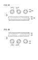
- FIG. 4A is a cross-sectional view taken along line IVA-IVA in FIG. 3
- FIG. 4B is a cross-sectional view taken along line IVB-IVB in FIG.
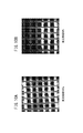
- FIG. 10A shows a captured image when the nitrogen emission region (N 2 emission region) is 100%
- FIG. 10B shows a captured image when the N 2 emission region is 50%. It is a nondestructive observation image (by X-ray CT) showing a state where pores having a diameter of 50 ⁇ m exist in the first ceramic layer.
- ⁇ indicating a numerical range is used as a meaning including numerical values described before and after the numerical value as a lower limit value and an upper limit value.
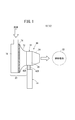
- the sterilization apparatus 10 is obtained by applying the plasma processing apparatus 12 shown in FIG.
- the plasma processing apparatus 12 includes a pulse power source 14 that generates a high voltage pulse and a reactor 16 that generates plasma by applying a high voltage pulse from the pulse power source 14.
- the reactor 16 has an anode and a cathode.
- the reactor 16 generates a discharge between the anode and the cathode based on the supply of a high voltage pulse from the pulse power supply 14.
- the reactor 16 guides fluid to the discharge electrode 18. And a nozzle 24 that outputs the fluid that has passed through the discharge electrode portion 18 toward the workpiece 22.
- the plasma processing apparatus 12 generates plasma by discharge in the discharge electrode portion 18 while introducing a fluid into the discharge electrode portion 18, and applies the excited substance together with the fluid to the object 22 to be processed. At least the surface of 22 is treated. Therefore, the to-be-processed object 22 can be sterilized by applying this plasma processing apparatus 12 to the sterilization process to make the sterilization apparatus 10.
- At least one of the fluid guide unit 20 and the nozzle 24 has a structure in which the flow path area gradually decreases in the fluid flow direction.
- Excited substances include radicals (chemically active species), excited species (molecules whose internal energy state has changed (excited state) due to high-speed electron collision, ions, luminescent species, This refers to a molecule (for example, ozone) generated by an excited substance reacting with a fluid molecule.
- the discharge electrode portion 18 includes a first discharge electrode 26A serving as an anode, a second discharge electrode 26B serving as a cathode, and a predetermined positional relationship between the first discharge electrode 26A and the second discharge electrode 26B.
- a case 28 (see FIGS. 1 and 6).
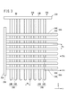
- the first discharge electrode 26 ⁇ / b> A extends in the first direction (x direction) and is arranged in a second direction (y direction) orthogonal to the first direction and has a plurality of rod-shaped first conductors 30 ⁇ / b> A. And a first common conductor 32A that connects the plurality of first conductors 30A, and a first ceramic layer 34A that covers at least the first conductor 30A.
- the first conductor 30A and the portion of the first ceramic layer 34A that covers the first conductor 30A are referred to as a first electrode portion 36A.
- the second discharge electrode 26B extends in the second direction (y direction) and has a plurality of rod-like second conductors 30B arranged in the first direction (x direction) and a second common connecting the plurality of second conductors 30B. It has a conductor 32B and a second ceramic layer 34B covering at least the second conductor 30B. A portion of the second conductor 30B and the second ceramic layer 34B covering the second conductor 30B is referred to as a second electrode portion 36B.
- first conductor 30A and the second conductor 30B copper, iron, tungsten, stainless steel, platinum, or the like can be used.
- first ceramic layer 34A and the second ceramic layer 34B alumina, silica, titania, zirconia, or the like can be used.
- the diameters d1 and d2 of the first conductor 30A and the second conductor 30B are 200 to 1000 ⁇ m.
- both the first ceramic layer 34A covering the first conductor 30A and the second ceramic layer 34B covering the second conductor 30B do not have pores of 50 ⁇ m or more inside. If the porosity is large enough to be expressed as a percentage, the voltage applied to the ceramics may cause a dielectric breakdown. Even if there is only one closed pore of 50 ⁇ m in total, there is a risk that dielectric breakdown will occur from the closed pore portion, arc plasma will be generated, and the ceramic will be dissolved. Ideally, there are no closed pores, and it is desirable that all closed pores dispersed in the material have a diameter of less than 10 ⁇ m.
- the area of the first conductor 30A is Aa1
- the area of the first ceramic layer 34A is Ab1
- the second electrode portion 36B is orthogonal to the axial direction.
- the electric field strength is lowered, the energy given to the electrons is lowered, and the generation of radicals is reduced. Since this corresponds to an increase in the dielectric between the first conductor 30A and the second conductor 30B, the capacitance component apparently increases, making it difficult to obtain a steep voltage increase rate (dV / dt). Therefore, it is desirable that the range is as described above.
- the diameters d1 and d2 of the first conductor 30A and the second conductor 30B affect the electric field strength.
- the anode (first conductor 30A) to which a high voltage is applied has a higher electric field strength on the surface as the diameter d1 is smaller.
- the first conductor 30A and the second conductor 30B are preferably thin, but there is a limit in maintaining strength and shape. Therefore, the diameter d1 of the first conductor 30A is preferably 0.2 to 0.5 mm, and the thickness t1 of the first ceramic layer 34A is preferably 0.25 to 0.65 mm.
- the diameter d2 of the second conductor 30B is preferably 0.5 to 1.0 mm, and the thickness t2 of the second ceramic layer 34B is preferably 0.25 to 1.25 mm.
- the case 28 is provided with, for example, a circular through-hole through which fluid flows in the center, and the first common conductor 32A (see FIG. 3) and the positive-side wiring 40A from the pulse power supply 14 (see FIG. 1) are provided inside the outer periphery. ) And a connection portion between the second common conductor 32B (see FIG. 3) and the negative electrode side wiring 40B (see FIG. 1) from the pulse power supply 14 are accommodated.
- the first discharge electrode 26A and the second discharge electrode 26B are mounted in the case 28, the plurality of first electrode portions 36A and the plurality of second electrode portions 36B face each other, and the discharge electrode portion 18 When viewed from the fluid flow direction, the first electrode portion 36A and the second electrode portion 36B (see FIG. 3) are held in a crossed positional relationship (a twisted positional relationship). That is, the first conductor 30 ⁇ / b> A and the second conductor 30 ⁇ / b> B are held in a positional relationship (a twisted positional relationship) where they intersect. At this time, a portion where the first electrode portion 36 ⁇ / b> A and the second electrode portion 36 ⁇ / b> B intersect is exposed through the through hole of the case 28.
- the first electrode portion 36A (first conductor 30A) and the second electrode portion 36B (second conductor 30B) have a plurality of lattices. Is formed.
- the arrangement pitch of the intersecting portion between the first electrode portion 36A (first conductor 30A) and the second electrode portion 36B (second conductor 30B) is 5 to 50 mm.
- the opening ratio of the discharge electrode portion 18 is 30 to 50%.
- the arrangement pitch Pb of the second electrode part 36B serving as the cathode may be as small as about 1 to 10 mm, for example, but the arrangement pitch Pa of the first electrode part 36A serving as the anode is the separation distance dc from the second electrode part 36B. It is preferable to set a positive correlation with (gap: see FIGS. 4A and 4B). That is, the arrangement pitch Pa of the first electrode portions 36A is increased as the distance dc from the second electrode portions 36B increases. For example, when the separation distance dc is 5 mm, the arrangement pitch Pa of the first electrode portions 36A is set to 5 mm or more, and when the separation distance dc is 40 mm, the arrangement pitch Pa of the first electrode portions 36A is set to 30 mm or more.
- the arrangement pitch Pa of the first electrode portions 36A is set to 50 mm or more. However, if the arrangement pitch Pa of the first electrode portions 36A is too far away, the discharge area is reduced. Therefore, the arrangement pitch Pa of the first electrode portions 36A is preferably 50 to 100% of the separation distance dc.
- the aperture ratio of the discharge electrode portion 18 is smaller than 30%, it is sufficiently wide for fluid molecules and hardly affected. However, it is the electric field strength and the voltage increase rate (dV / dt) on the anode surface that most affect the radical generation efficiency. As described above, the reason why the arrangement pitch Pa of the first electrode portions 36A that are anodes is increased in accordance with the separation distance dc is to maintain the electric field strength high.
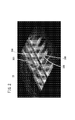
- FIG. 2 shows a state in which plasma is generated between the first electrode portion 36A of the first discharge electrode 26A and the second electrode portion 36B of the second discharge electrode 26B.
- the pulse power supply 14 includes a pulse generator 41 that applies a high voltage pulse between the anode and the cathode, and a pulse controller that controls the pulse generator 41 so as to generate a discharge between the anode and the cathode. 42.
- the pulse generation unit 41 includes a pulse generation circuit 43 having the following configuration, for example. That is, the pulse generation circuit 43 includes a DC power supply unit 46 having a DC power supply 44 that supplies DC and a capacitor 45 that stabilizes the supply of DC from the DC power supply 44, a transformer 47 that accumulates inductive energy, and a transformer 47 DC supply path 50 to the primary winding 48, MOSFET (metal oxide semiconductor field effect transistor) 52 and SI thyristor 54 for opening and closing the supply path 50, bias application path 56 to the gate of the SI thyristor 54, SI A diode 58 that suppresses a current from flowing into the gate of the thyristor 54 and allows a current to flow out of the gate of the SI thyristor 54, and an output path 62 of a pulse voltage from the secondary winding 60 of the transformer 47.
- the pulse control unit 42 includes a drive circuit 64 that drives the MOSFET 52.
- the SI thyristor 54 and the MOSFET 52 are inserted in series in the supply path 50 so as to close the supply path 50 when turned on and open the supply path 50 when turned off.
- One end 66 a of the primary winding 48 is connected to the positive electrode of the DC power supply 44 and one end of the capacitor 45
- the anode of the SI thyristor 54 is connected to the other end 66 b of the primary winding 48
- the cathode of the SI thyristor 54 is the drain of the MOSFET 52.
- the source of the MOSFET 52 is connected to the negative electrode of the DC power supply 44 and the other end of the capacitor 45.
- the gate of the SI thyristor 54 is connected to one end 66 a of the primary winding 48 via a diode 58 by a bias applying path 56.
- the cathode of the diode 58 is connected to one end 66 a of the primary winding 48, and the anode of the diode 58 is connected to the gate of the SI thyristor 54.
- the diode 58 causes the SI thyristor 54 to be positively biased by voltage driving and negatively biased by current driving.
- An inductor having a single winding may be used in place of the transformer 47, and the pulse voltage may be output directly from the inductor.
- the gate of the SI thyristor 54 is negatively biased by the induced electromotive force generated in the primary winding 48, and the SI thyristor 54 is also turned off at high speed.
- the supply path 50 is opened at high speed.
- an induced electromotive force is generated in the secondary winding 60 due to mutual induction, and the rate of time increase of the voltage V at the time of rise between the positive winding 68 and the negative electrode 70 from the secondary winding 60.
- a pulse voltage with a remarkably large dV / dt is output.
- the pulse width of the pulse voltage is preferably about 10 to 1000 ns in terms of the full width at half maximum (FWHM), and the time rise rate dV / dt of the voltage V at the time of rising is preferably about 30 to 3000 kV / ⁇ s.
- the number of repetitions per unit time is preferably about 100 pps to several hundred kpps. The reason why the desired range is described as “generally” is that the desired range may be wider than the above range depending on the structure, material, fluid pressure, and fluid flow rate of the reactor 16.
- pulse power supply 14 More detailed operating principles of the pulse power supply 14 are described in, for example, Katsuji Iida, Ken Sakuma: “Ultra-short pulse generation circuit (IES circuit) by SI thyristor”, SI Device Symposium Proceedings (2002).
- the fluid guide part 20 has a rectifying structure for uniformly supplying the fluid to the discharge electrode part 18 as shown in FIGS.
- the rectifying structure includes a bell mouth portion 72, a rectifying network portion 74, and a fluid inflow case 76.
- the bell mouth portion 72 is installed on the upstream side of the discharge electrode portion 18 and has a bell mouth structure in which the flow path area gradually decreases in the fluid flow direction.
- the rectifying network part 74 is installed on the upstream side of the bell mouth part 72 and includes one or more rectifying networks 78 and a pressing frame 80 that presses the rectifying network 78 from both sides (upstream side and downstream side).
- the opening ratio of the rectifying network 78 is desirably 10 to 45%, but the opening ratio may be lower depending on the opening area of the bell mouth portion 72. The reason is that the rectifying network portion 74 serves to uniformly feed the fluid having various velocity vectors entering the fluid inflow case 76 to the bell mouth portion 72. It is desirable that the number of meshes is large and the aperture ratio is low.
- the opening diameter of the bell mouth portion 72 is as large as 30 mm, for example, there is no problem even if the opening ratio is as low as it is a commercially available mesh. If the inner diameter of the conduit 82 described later is, for example, 6 mm, the opening area of the bell mouth portion 72 is 25 times the opening area of the conduit 82 if the opening diameter of the bell mouth portion 72 is 30 mm. Accordingly, no pressure loss occurs even when the aperture ratio is 4%.
- the fluid inflow case 76 is installed on the upstream side of the rectifying network part 74, and the inner dimension Da in the fluid outlet direction to the bell mouth part 72 has a positive correlation with the fluid flow rate.
- the internal dimension Da is 20 mm to 100 mm when the fluid flow rate is in the range of 10 to 20 liters / min.
- the direction of fluid supply to the fluid inflow case 76 is different from the direction of fluid delivery to the bell mouth portion 72. That is, the supply of the fluid to the fluid inflow case 76 is performed through the conduit 82 provided on one surface of the fluid inflow case 76, and the angle between the fluid supply direction m and the fluid outlet direction n is 80 ° to 100 °. °.
- a conduit 82 is provided on a surface (for example, the upper surface) parallel to the fluid outlet direction n to the bell mouth portion 72, and the fluid supply direction m and the fluid outlet The angle formed with the direction n is approximately 90 °.
- the nozzle 24 may be a first nozzle 24A having a bell mouth structure in which the flow path area gradually decreases in the direction of fluid flow, or a square nozzle-shaped second nozzle 24B.
- the plasma processing apparatus 12 has the anode and the cathode, and generates the discharge between the anode and the cathode based on the supply of the high voltage pulse from the pulse power supply 14.
- a fluid guide unit 20 that guides the fluid to the discharge electrode unit 18, and a nozzle 24 that injects at least excited species generated in the fluid by discharge at the discharge electrode unit 18 into the workpiece 22. Since at least one of the guide unit 20 and the nozzle 24 has a structure in which the flow path area gradually decreases in the fluid flow direction, the fluid flows uniformly to the discharge electrode unit 18. Therefore, plasma can be efficiently generated in the discharge electrode portion 18. Therefore, the efficiency of the sterilization treatment can be improved when the sterilization treatment is performed by indirectly applying the excited substance due to the generation of plasma to the workpiece 22.
- the first conductor 30A is set in a mold, a slurry containing a ceramic powder, a dispersion medium, and a gelling agent is cast, and then the slurry is gelled by adding temperature conditions and a crosslinking agent.
- the first discharge electrode 26 ⁇ / b> A is manufactured by solidifying, forming, and then firing.
- the second discharge electrode 26B can also be produced by a similar method. According to this gel cast method, since the slurry is mixed with the first conductor 30A through the low viscosity state of the slurry, voids hardly remain after mixing. Therefore, even if the first discharge electrode 26A is manufactured by firing after forming, the first ceramic layer 34A is kept in a dense state. The same applies to the second ceramic layer 34B.
- the first electrode portion 36A and the second electrode portion 36B are each comb-shaped.
- Both the conductor 30A and the second conductor 30B may be formed in a lattice shape.
- the first electrode portion 36A (first conductor 30A) and the second electrode portion 36B (second conductor 30B) intersect each other when viewed from the fluid flow direction with respect to the discharge electrode portion 18, that is, the first It is installed in a state where the intersection of the second electrode part 36B is located in the opening of the first electrode part 36A.
- the first electrode portion 36A and the second electrode portion 36B are each formed in a lattice shape, and the first conductor 30A in the first electrode portion 36A and the second electrode portion 36B Each of the second conductors 30B may be comb-shaped.
- the first ceramic layer 34A of the first electrode portion 36A is configured in a lattice shape, and the first conductors 30A in the first ceramic layer 34A are extended in, for example, the x direction and arranged in the y direction.
- the second ceramic layer 34B of the second electrode portion 36B is configured in a lattice shape, and the second conductors 30B in the second ceramic layer 34B extend, for example, in the y direction and are arranged in the x direction.
- the first portion 84A (the portion extending in the y direction and arranged in the x direction) in which the first conductor 30A is not formed is the first conductor. It is sufficient that the strength between the first electrode portions 36A composed of 30A and the first ceramic layer 34A can be maintained.
- the second portion 84B (the portion extending in the x direction and arranged in the y direction) in which the second conductor 30B is not layered is the second conductor 30B and the second ceramic. It is sufficient that the strength between the second electrode portions 36B formed of the layer 34B can be maintained.
- the first portion 84A in which the first conductor 30A is not layered is thinned out of the first ceramic layer 34A, and similarly, in the second ceramic layer 34B, The second portion 84B in which the second conductor 30B is not layered may be thinned out.
- the example of FIG. 9 shows a case where the first part 84A and the second part 84B are thinned out one by one. Of course, two to several pieces may be thinned out as long as the strength between the first electrode portions 36A and the strength between the second electrode portions 36B can be maintained.
- the supply flow rate of the fluid (nitrogen N 2 ) and the dimensions of the plasma processing apparatus 12 are as follows.
- N 2 emission region the ratio of the nitrogen emission region (referred to as N 2 emission region) to the entire region where the first electrode portion 36A and the second electrode portion 36B intersect was obtained as a percentage.
- FIG. 10A shows the state of the N 2 light emitting region 100%
- FIG. 10B shows the state of the N 2 light emitting region 50%.
- Examples 1 to 6 In Examples 1, 2, 3, 4, 5, and 6, the opening ratio of the rectifying network portion 74 was 16%, 21%, 23%, 28%, 37%, and 41%, respectively.
- the N 2 emission region of Reference Examples 1 and 2 was 50%, but in Examples 1 to 6, the N 2 emission region was 70% or more and was good. In particular, in Examples 1 to 3, the N 2 emission region was 100%. From this, it can be seen that the smaller the aperture ratio of the rectifying network portion 74, the more the fluid rectifying property is improved and the discharge is stably performed over the entire discharge electrode portion 18. However, as in Reference Example 1, when the aperture ratio becomes extremely small, the fluid rectification property is deteriorated and the discharge becomes unstable. Accordingly, it can be seen that the preferable range of the aperture ratio of the rectifying network portion 74 is preferably 16% to 41%, and more preferably 16% to 23%.
- the confirmation of the measurement conditions and the light emitting area is the same as in the first embodiment described above, but the aperture ratio of the rectifying network 74 is 23%.
- Example 11 to 13 In Examples 11, 12, and 13, the inner dimension Da in the fluid outlet direction of the fluid inflow case 76 was 30 mm, 60 mm, and 100 mm, respectively, and the fluid flow rate was 10 (liters / min).
- Example 14 and 15 In Examples 14 and 15, the inner dimension Da of the fluid inflow case 76 in the fluid outlet direction was 60 mm and 100 mm, respectively, and the fluid flow rate was 20 (liter / min).
- the internal dimension Da of the fluid inflow case 76 in the fluid outlet direction is 10 mm, 10 mm, and 30 mm, respectively, and the fluid flow rates are 10 (liter / min), 20 (liter / min), and 20 ( Liter / min).
- the N 2 emission region of Reference Example 12 was 30% and the N 2 emission region of Reference Examples 11 and 13 was 50%, but in Examples 11 to 15, all of the N 2 emission region was 100%. It was good. From this, it can be seen that the larger the inner dimension Da of the fluid inflow case 76 in the fluid outlet direction, the better the fluid rectification, and the larger the flow rate, the larger the inner dimension Da must be. Therefore, there is a lower limit value of the inner dimension Da in the fluid outlet direction of the fluid inflow case 76 for each flow rate, and the lower limit value is 30 mm at 10 liters / min and 60 mm at 20 liters / min.
- the confirmation of the measurement conditions and the light emitting area is the same as in the first embodiment described above, but the aperture ratio of the rectifying network 74 is 23%.
- Example 21 to 23 In Examples 21, 22, and 23, the arrangement pitch Pa of the anode was 3 mm, 6 mm, and 10 mm, respectively, and the distance dc between the anode and the cathode was 5 mm.
- Example 24 In Examples 24, 25, and 26, the arrangement pitch Pa of the anode was set to 30 mm, 40 mm, and 50 mm, respectively, and the distance dc between the anode and the cathode was set to 40 mm.
- Example 27 and 28 In Examples 27 and 28, the anode arrangement pitch Pa was 50 mm and 80 mm, respectively, and the distance dc between the anode and the cathode was 100 mm.
- N 2 emission region of Reference Example 21, 22 and 24 is 50%, but N 2 emission region of Reference Example 23 was 30% Examples 21 to 28, are both N 2 emission region It was 80% or more and was good. In particular, in Examples 21, 22, 24, 25, and 27, the N 2 emission region was 100%. From the experimental results, it has been found that as the distance dc between the anode and the cathode is increased, the discharge at the center is weakened unless the anode arrangement pitch Pa is increased. On the other hand, it was found that even if the anode arrangement pitch Pa is too wide, a cold spot region is formed in the plasma, and the efficiency is lowered. Therefore, the anode arrangement pitch Pa is desirably 50% to 100% of the distance dc between the anode and the cathode.
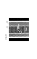
- FIG. 11 shows a state in which pores having a diameter of 50 ⁇ m are present in the first ceramic layer 34A.
- FIG. 11 is a nondestructive observation image by X-ray CT.
- Example 31 to 36 In Examples 31, 32, 33, 34, 35, and 36, the size of pores existing in the first ceramic layer 34A is 30 ⁇ m, 30 ⁇ m, 20 ⁇ m, 15 ⁇ m, 15 ⁇ m, and 10 ⁇ m.
- the size of pores present in the first ceramic layer 34A is 50 ⁇ m and 70 ⁇ m.
- Examples 41, 42, 43, 44, 45, and 46 have cross-sectional area ratios (Aa1 / Ab1) of 0.15, 0.3, 0.5, 0.7, 0.8, and 0.9, respectively. .
- the plasma emission intensity of Reference Example 41 was 0.1, but all of Examples 41 to 46 were good with a plasma emission intensity of 0.5 or more. In particular, Examples 44, 45, and 46 had plasma emission intensity of 0.9, 0.9, and 1.0. On the other hand, Reference Example 42 was damaged although the plasma emission intensity was 1.0. From this, it can be seen that the smaller the cross-sectional area of the first ceramic layer 34A, the higher the voltage applied to the surface of the first conductor 30A, and the higher the plasma emission intensity. However, if the first ceramic layer 34A is made too thin, dielectric breakdown tends to occur, and even a small pore easily causes a large electric field concentration and is easily damaged. Therefore, it can be seen that the cross-sectional area ratio (Aa1 / Ab1) is 0.1 ⁇ Aa1 / Ab1 ⁇ 1.0.
- Example 51 In Examples 51, 52, 53, 54, 55, and 56, the cross-sectional area ratio (Aa2 / Ab2) is 0.1, 0.5, 1.0, 1.3, 1.5, and 1.8, respectively. .
- the plasma emission intensity of Reference Example 51 was 0.3, but all of Examples 51 to 56 were good with plasma emission intensity of 0.6 or more. In particular, Examples 53, 54, 55, and 56 had plasma emission intensity of 0.9, 0.9, 0.9, and 1.0. On the other hand, in Reference Example 52, the plasma emission intensity was 1.0, but it was damaged. From this, it can be seen that the voltage applied to the surface of the second conductor 30B increases and the plasma emission intensity increases as the cross-sectional area of the second ceramic layer 34B decreases, as in the fifth embodiment. However, if the second ceramic layer 34B is made too thin, dielectric breakdown tends to occur, and even a small pore tends to cause a large electric field concentration and be easily damaged. Therefore, it can be seen that the cross-sectional area ratio (Aa2 / Ab2) is 0.08 ⁇ Aa2 / Ab2 ⁇ 2.0.
- Example 61 to 66 In Examples 61, 62, 63, 64, 65, and 66, the diameter d1 of the first conductor 30A is 200 ⁇ m, 300 ⁇ m, 500 ⁇ m, 800 ⁇ m, 900 ⁇ m, and 1000 ⁇ m, respectively.
- the diameter d1 of the first conductor 30A is 100 ⁇ m and 1200 ⁇ m, respectively.
- Table 7 shows that the smaller the diameter d1 of the first conductor 30A, the higher the electric field strength, the higher the percentage of high-energy electrons, and the greater the number of active species generated from the plasma. On the other hand, the wire is easily cut and the reliability of the plasma processing apparatus is lowered. In Reference Example 61, the plasma emission intensity was 1.0, but there is anxiety in terms of reliability. Accordingly, the diameter d1 of the first conductor 30A is preferably 200 to 1000 ⁇ m, more preferably 300 to 500 ⁇ m.
- sterilization apparatus is not limited to the above-described embodiment, and various configurations can be adopted without departing from the gist of the present invention.
Landscapes
- Physics & Mathematics (AREA)
- Engineering & Computer Science (AREA)
- Plasma & Fusion (AREA)
- Spectroscopy & Molecular Physics (AREA)
- Health & Medical Sciences (AREA)
- Epidemiology (AREA)
- Life Sciences & Earth Sciences (AREA)
- Animal Behavior & Ethology (AREA)
- General Health & Medical Sciences (AREA)
- Public Health (AREA)
- Veterinary Medicine (AREA)
- Apparatus For Disinfection Or Sterilisation (AREA)
- Plasma Technology (AREA)
Abstract
本発明に関する殺菌装置は、パルス電源(14)からの高電圧パルスの供給に基づいて陽極と陰極間に放電を発生させる放電電極部(18)と、放電電極部(18)に流体を案内する流体案内部(20)と、放電電極部(18)を通過した流体を被処理物(22)に向けて出力するノズル(24)とを有する。この殺菌装置は、放電電極部(18)に流体を導入しながら、放電電極部(18)において放電によりプラズマを発生させ、その励起物を流体と共に被処理物(22)に当て、流体案内部(20)及びノズル(24)のうち、少なくとも1つは、流路面積が流体の流通方向に向かって徐々に小さくなる構造を有する。
Description
本発明は、パルス電源からの高電圧パルスによる放電によって発生したプラズマを利用して対象物の少なくとも表面を殺菌する殺菌装置に関する。
近時、プラズマ中の活性中性粒子を用いて、農作物や食品等の殺菌を行う試みがなされている(文献:IEEJ Journal,Vol.132 No.10.2012 p.702~705「プラズマの農業応用-農産物殺菌から植物成長制御まで-」参照)。
ラジカルを生成する装置としては、上述した文献に記載された大気圧バリア放電プラズマトーチのほか、国際公開第2011/065171号パンフレット及び国際公開第2012/120928号パンフレットに記載された装置が知られている。
国際公開第2011/065171号パンフレットに記載の装置は、第1の電極、第2の電極及び第3の電極からなる電極構成体を、ガスの流路の途中に設置し、第2の電極を第1の電極より上流側に設置し、第3の電極を第1の電極より下流側に設置して構成される。そして、パルス電源の一方の極を第1の電極に接続し、パルス電源の他方の極を第2の電極及び第3の電極に接続する。さらに、第1の電極を、第1のガス通過面を横切り、且つ、第1のガス通過面の一部を占めるように設置し、第2の電極及び第3の電極を、それぞれ第2のガス通過面及び第3のガス通過面を横切り、且つ、第2のガス通過面及び第3のガス通過面の一部を占めるように設置する。これにより、第1の電極より上流側及び下流側にプラズマが発生することとなる。また、第1の電極、第2の電極及び第3の電極の各末端が、放電の始点又は終点とならず、第1の電極、第2の電極及び第3の電極の耐久性が向上する。
国際公開第2012/120928号パンフレットに記載の装置は、導電体で構成された筐体内に、流路形成物、トランス、電極構成体(陽極棒及び陰極板)、陽極側の給電経路及び陰極側の給電経路が収容されて構成される。陽極棒の延在方向と陰極板の延在方向とは非平行とされ、陽極棒及び陰極板はガス流路を横断する。陽極棒と陰極板とはガス流路の延在方向に離間して配置される。陽極棒の給電端とパルス電源の二次側巻線の正出力端とを電気的に接続し、陰極板の給電端と二次側巻線の負出力端とを電気的に接続し、さらに、筐体を陰極側の給電経路に電気的に接続する。これにより、パルス電圧の波形が乱れにくくなる。
しかしながら、上述した文献並びに国際公開第2011/065171号パンフレット及び国際公開第2012/120928号パンフレットには、電極構成体に対してガスを均一に流す機構について考慮しておらず、また、電極構成体を構成する陽極及び陰極の各構成部材のパラメータの最適化も検討されていないため、電極構成体で効率よくプラズマを発生させることが困難である。そのため、従来技術では、プラズマの発生による励起物を間接的に被処理物に当てて殺菌等のプラズマ処理を行う場合に、プラズマ処理の効率化に限界が生じるという問題が内在している。
本発明はこのような課題を考慮してなされたものであり、放電電極部に対して流体を均一に流すことが可能で、放電電極部において効率よくプラズマを発生させることができ、プラズマの発生による励起物を間接的に被処理物に当てて殺菌処理を行う場合に、殺菌処理の効率化を図ることができる殺菌装置を提供することを目的とする。
[1] 第1の本発明に係る殺菌装置は、パルス電源からの高電圧パルスによる放電によって発生したプラズマを利用して対象物の少なくとも表面を殺菌する殺菌装置において、陽極と陰極とを有し、前記パルス電源からの前記高電圧パルスの供給に基づいて前記陽極と前記陰極間に放電を発生させる放電電極部と、前記放電電極部に流体を案内する流体案内部と、前記放電電極部を通過した前記流体を前記対象物に向けて出力するノズルと、を有し、前記放電電極部に前記流体を導入しながら、前記放電電極部において前記放電によりプラズマを発生させ、その励起物を前記流体と共に前記対象物に当て、前記流体案内部及び前記ノズルのうち、少なくとも1つは、流路面積が前記流体の流通方向に向かって徐々に小さくなる構造を有することを特徴とする。
これにより、放電電極部に対して流体を均一に流すことが可能で、放電電極部において効率よくプラズマを発生させることができ、プラズマの発生による励起物を間接的に被処理物に当てて殺菌処理を行う場合に、殺菌処理の効率化を図ることができる。
[2] 第1の本発明において、前記流体案内部は、前記流体を前記放電電極部に対して均一に供給する整流構造を有してもよい。
[3] この場合、前記整流構造は、流路面積が前記流体の流通方向に向かって徐々に小さくなるベルマウス構造と、前記ベルマウス構造の上流側に設置された1以上の整流網と、前記ベルマウス構造への流体導出方向の内寸が流体流量と正の相関関係にある流体流入ケースと、を有してもよい。
[4] さらに、前記整流網の開口率が10~45%であってもよい。
[5] また、前記流体流入ケースの前記ベルマウス構造への流体導入方向の内寸は、流体流量10リットル/minから20リットル/minにおいて20mm~100mmであってもよい。
[6] 前記流体案内部への前記流体の供給方向が、前記放電電極部への前記流体の流通方向と異なってもよい。
[7] この場合、前記流体の供給方向と前記流体の流通方向とのなす角が80°~100°であってもよい。
[8] 第1の本発明において、前記ノズルは、流路面積が前記流体の流通方向に向かって徐々に小さくなる構造を有してもよい。
[9] 第1の本発明において、前記放電電極部は、前記陽極となる第1放電電極と、前記陰極となる第2放電電極とを有し、前記第1放電電極を構成する複数の第1導体と、前記第2放電電極を構成する複数の第2導体とが、互いに離間し、且つ、前記放電電極部に対する前記流体の流通方向から見たときに、前記第1導体と前記第2導体とが交差した位置関係にあってもよい。
[10] 第1の本発明において、前記放電電極部は、前記陽極となる第1放電電極と、前記陰極となる第2放電電極とを有し、前記第1放電電極を構成する複数の第1導体と、前記第2放電電極を構成する複数の第2導体とが、ねじれの位置関係にあってもよい。
[11] 前記放電電極部に対する前記流体の流通方向から見たときに、前記第1導体と前記第2導体とで複数の格子が形成されてもよい。
[12] 前記第1導体と前記第2導体との交差部分の配列ピッチが5~50mmであってもよい。
[13] また、前記放電電極部に対する前記流体の流通方向から見たときに、前記放電電極部の開口率が30~50%であってもよい。
[14] 前記第1放電電極は、前記第1導体と、該第1導体を被覆する第1セラミック層とを有し、前記第2放電電極は、前記第2導体と、該第2導体を被覆する第2セラミック層とを有してもよい。
[15] 前記第1セラミック層及び前記第2セラミック層の内部に50μm以上の気孔を有しないことが好ましい。
[16] 前記第1導体と前記第1セラミック層を、軸方向に直交する方向に切断した断面において、前記第1導体の面積をAa1、前記第1セラミック層の面積をAb1とし、前記第2導体と前記第2セラミック層を、軸方向に直交する方向に切断した断面において、前記第2導体の面積をAa2、前記第2セラミック層の面積をAb2としたとき、
0.1<Aa1/Ab1<1.0
0.08<Aa2/Ab2<2.0
であることが好ましい。
0.1<Aa1/Ab1<1.0
0.08<Aa2/Ab2<2.0
であることが好ましい。
[17] この場合、前記第1導体及び前記第2導体の各直径が200~1000μmであることが好ましい。
[18] 第1の本発明において、前記パルス電源は、前記陽極及び前記陰極間に前記高電圧パルスを印加するパルス発生部と、前記陽極及び前記陰極間に放電を発生させるように前記パルス発生部を制御するパルス制御部とを有し、前記パルス発生部は、直流電源部の両端に直列接続されたトランス及びスイッチを有し、前記パルス制御部の前記スイッチに対するオン制御によって前記トランスへの誘導エネルギーの蓄積を行い、前記パルス制御部の前記スイッチに対するオフ制御によって前記トランスの二次側での前記高電圧パルスの発生を行うパルス発生回路を有してもよい。
[19] 第2の本発明に係るプラズマ処理装置は、パルス電源からの高電圧パルスによる放電によって発生したプラズマを利用して対象物の少なくとも表面を処理するプラズマ処理装置において、陽極と陰極とを有し、前記パルス電源からの前記高電圧パルスの供給に基づいて前記陽極と前記陰極間に放電を発生させる放電電極部と、前記放電電極部に流体を案内する流体案内部と、前記放電電極部を通過した前記流体を前記対象物に向けて出力するノズルと、を有し、前記放電電極部に前記流体を導入しながら、前記放電電極部において前記放電によりプラズマを発生させ、その励起物を前記流体と共に前記対象物に当て、前記流体案内部及び前記ノズルのうち、少なくとも1つは、流路面積が前記流体の流通方向に向かって徐々に小さくなる構造を有することを特徴とする。
これにより、放電電極部に対して流体を均一に流すことが可能で、放電電極部において効率よくプラズマを発生させることができ、プラズマの発生による励起物を間接的に被処理物に当てて、少なくとも被処理物の表面処理を行う場合に、表面処理の効率化を図ることができる。もちろん、上述した殺菌装置やその他の装置に適用させることができ、汎用性に富む。
以上説明したように、本発明に係る殺菌装置によれば、放電電極部に対して流体を均一に流すことが可能で、放電電極部において効率よくプラズマを発生させることができ、プラズマの発生による励起物を間接的に被処理物に当てて殺菌処理を行う場合に、殺菌処理の効率化を図ることができる。
以下、本発明に係る殺菌装置の実施の形態例を図1~図11を参照しながら説明する。なお、本明細書において数値範囲を示す「~」は、その前後に記載される数値を下限値及び上限値として含む意味として使用される。
本実施の形態に係る殺菌装置10は、図1に示すプラズマ処理装置12を殺菌装置10に適用したものである。このプラズマ処理装置12は、高電圧パルスを発生するパルス電源14と、パルス電源14からの高電圧パルスの印加によってプラズマを発生するリアクタ16とを有する。
リアクタ16は、陽極と陰極とを有し、且つ、パルス電源14からの高電圧パルスの供給に基づいて陽極と陰極間に放電を発生させる放電電極部18と、放電電極部18に流体を案内する流体案内部20と、放電電極部18を通過した流体を被処理物22に向けて出力するノズル24とを有する。
そして、このプラズマ処理装置12は、放電電極部18に流体を導入しながら、放電電極部18において放電によりプラズマを発生させ、その励起物を流体と共に被処理物22に当てて、該被処理物22の少なくとも表面を処理する。従って、このプラズマ処理装置12を殺菌処理に適用して殺菌装置10とすることで、被処理物22の殺菌を行うことができる。流体案内部20及びノズル24のうち、少なくとも1つは、流路面積が流体の流通方向に向かって徐々に小さくなる構造を有する。「励起物」は、ラジカル(化学活性種)、励起種(分子が、高速な電子の衝突により、形態は変わらず内部のエネルギー状態が変化(励起状態)したもの)、イオン、発光種、さらに励起物が流体分子と反応して生成した分子(例えばオゾン)等を指す。
放電電極部18は、図2に示すように、陽極となる第1放電電極26Aと、陰極となる第2放電電極26Bと、これら第1放電電極26A及び第2放電電極26Bを所定の位置関係で保持するケース28(図1、図6参照)とを有する。
図3に示すように、第1放電電極26Aは、第1方向(x方向)に延び、且つ、第1方向と直交する第2方向(y方向)に配列した棒状の複数の第1導体30Aと、複数の第1導体30Aをつなぐ第1共通導体32Aと、少なくとも第1導体30Aを被覆する第1セラミック層34Aとを有する。第1導体30Aと該第1導体30Aを被覆する第1セラミック層34Aの部分を第1電極部36Aと記す。
第2放電電極26Bは、第2方向(y方向)に延び、且つ、第1方向(x方向)に配列した棒状の複数の第2導体30Bと、複数の第2導体30Bをつなぐ第2共通導体32Bと、少なくとも第2導体30Bを被覆する第2セラミック層34Bとを有する。第2導体30Bと該第2導体30Bを被覆する第2セラミック層34Bの部分を第2電極部36Bと記す。
第1導体30A及び第2導体30Bとしては、銅、鉄、タングステン、ステンレス、白金等を用いることができる。第1セラミック層34A及び第2セラミック層34Bとしては、アルミナ、シリカ、チタニア、ジルコニア等を用いることができる。
図4A及び図4Bに示すように、第1導体30A及び第2導体30Bの各直径d1及びd2は200~1000μmである。また、第1導体30Aを被覆する第1セラミック層34A及び第2導体30Bを被覆する第2セラミック層34Bは共に、内部に50μm以上の気孔を有しない。なお、パーセンテージで表されるくらいに気孔率が大きいとセラミックスにかかる電圧でたちまち絶縁破壊するおそれがある。全体で1個でも50μmの閉気孔があるだけで、該閉気孔の部分から絶縁破壊し、アークプラズマとなりセラミックスが溶解するおそれがある。理想的には閉気孔は存在せず、材料中に分散する閉気孔の径が全て10μm未満であることが望ましい。
第1電極部36Aを軸方向に直交する方向に切断した断面において、第1導体30Aの面積をAa1、第1セラミック層34Aの面積をAb1とし、第2電極部36Bを軸方向に直交する方向に切断した断面において、第2導体30Bの面積をAa2、第2セラミック層34Bの面積をAb2としたとき、
0.1<Aa1/Ab1<1.0
0.08<Aa2/Ab2<2.0
である。
0.1<Aa1/Ab1<1.0
0.08<Aa2/Ab2<2.0
である。
第1セラミック層34A及び第2セラミック層34Bが厚いと電界強度が低下し、電子に与えるエネルギーが下がり、ラジカルの発生が少なくなる。これは、第1導体30Aと第2導体30B間の誘電体が増えることに相当するため、見かけ上、容量成分が増加し、急峻な電圧上昇率(dV/dt)を得難くなる。そこで、上述した範囲であることが望ましい。
第1導体30A及び第2導体30Bの各直径d1及びd2は電界強度に影響を与える。特に、高電圧がかかる陽極(第1導体30A)は直径d1が小さいほどその表面の電界強度は高くなる。従って、第1導体30A及び第2導体30Bは細い方が好ましいが、強度及び形状を保つためには限界がある。そこで、第1導体30Aの直径d1は、0.2~0.5mm、第1セラミック層34Aの厚みt1は0.25~0.65mmが好ましい。また、第2導体30Bの直径d2は、0.5~1.0mm、第2セラミック層34Bの厚みt2は0.25~1.25mmが好ましい。
ケース28は、中央に流体が流通する例えば円形の貫通孔が設けられ、外周部の内部には、第1共通導体32A(図3参照)とパルス電源14からの正極側配線40A(図1参照)との接続部分と、第2共通導体32B(図3参照)とパルス電源14からの負極側配線40B(図1参照)との接続部分とが収容されている。
そして、第1放電電極26Aと第2放電電極26Bをケース28内に取り付けた際に、複数の第1電極部36Aと複数の第2電極部36Bとが互いに対向し、且つ、放電電極部18に対する流体の流通方向から見たときに、第1電極部36Aと第2電極部36B(図3参照)とが交差した位置関係(ねじれの位置関係)で保持される。すなわち、第1導体30Aと第2導体30Bとが交差した位置関係(ねじれの位置関係)で保持される。このとき、第1電極部36Aと第2電極部36Bとが交差した部分がケース28の貫通孔を通じて露出した状態となる。
放電電極部18に対する流体の流通方向から見たときに、図3に示すように、第1電極部36A(第1導体30A)と第2電極部36B(第2導体30B)とで複数の格子が形成される。この場合、第1電極部36A(第1導体30A)と第2電極部36B(第2導体30B)との交差部分の配列ピッチが5~50mmである。また、放電電極部18に対する流体の流通方向から見たときに、放電電極部18の開口率は30~50%である。
陰極である第2電極部36Bの配列ピッチPbは、例えば1~10mm程度に小さくてもよいが、陽極である第1電極部36Aの配列ピッチPaは、第2電極部36Bとの離間距離dc(間隙:図4A及び図4B参照)と正の相関をとるように設定することが好ましい。すなわち、第2電極部36Bとの離間距離dcが大きくなるに従って第1電極部36Aの配列ピッチPaを広げる。例えば離間距離dcが5mmのとき、第1電極部36Aの配列ピッチPaを5mm以上に設定し、離間距離dcが40mmのとき、第1電極部36Aの配列ピッチPaを30mm以上に設定し、離間距離dcが100mmのとき、第1電極部36Aの配列ピッチPaを50mm以上に設定する。但し、第1電極部36Aの配列ピッチPaが離れすぎると、放電領域が少なくなるため、第1電極部36Aの配列ピッチPaは、離間距離dcの50~100%にすることが望ましい。
本来、放電電極部18の開口率が30%よりも小さくても、流体分子にとっては十分に広く、ほとんど影響を受けない。しかし、ラジカルの発生効率に最も影響するのが陽極表面の電界強度と電圧上昇速度(dV/dt)である。上述したように、陽極である第1電極部36Aの配列ピッチPaを、離間距離dcに応じて広げるのは、電界強度を高く維持するためである。
そして、パルス電源14の正極が第1放電電極26A(陽極)に接続され、パルス電源14の負極が第2放電電極26B(陰極)に接続される。これにより、第1放電電極26Aから第2放電電極26Bに向かう電界が第1電極部36Aと第2電極部36Bとの間隙に印加される。その結果、第2電極部36Bのうち、第1電極部36Aと対向する面の近傍にイオンシース層(イオンがたくさん集まった状態)が形成され、第1電極部36Aと第2電極部36Bとの間隙にプラズマが発生する。図2に第1放電電極26Aの第1電極部36Aと第2放電電極26Bの第2電極部36B間でプラズマが発生している状態を示す。
ここで、パルス電源14の構成について図5を参照しながら説明する。
パルス電源14は、図5に示すように、陽極及び陰極間に高電圧パルスを印加するパルス発生部41と、陽極と陰極間に放電を発生させるようにパルス発生部41を制御するパルス制御部42とを有する。
パルス発生部41は、例えば下記構成を有するパルス発生回路43を有する。すなわち、このパルス発生回路43は、直流を供給する直流電源44と直流電源44からの直流の供給を安定させるキャパシタ45とを有する直流電源部46と、誘導エネルギーを蓄積するトランス47と、トランス47の一次巻線48への直流の供給経路50と、供給経路50を開閉するMOSFET(酸化金属半導体電界効果トランジスタ)52及びSIサイリスタ54と、SIサイリスタ54のゲートへのバイアス付与経路56と、SIサイリスタ54のゲートへ電流が流入することを抑制し、SIサイリスタ54のゲートから電流が流出することを許容するダイオード58と、トランス47の二次巻線60からのパルス電圧の出力経路62とを有する。一方、パルス制御部42は、MOSFET52を駆動する駆動回路64を有する。
SIサイリスタ54及びMOSFET52は、ターンオンしたときに供給経路50を閉じ、ターンオフしたときに供給経路50を開くように、供給経路50に直列に挿入される。一次巻線48の一端66aは、直流電源44の正極及びキャパシタ45の一端に接続され、SIサイリスタ54のアノードは一次巻線48の他端66bに接続され、SIサイリスタ54のカソードはMOSFET52のドレインに接続され、MOSFET52のソースは直流電源44の負極及びキャパシタ45の他端に接続される。SIサイリスタ54のゲートは、バイアス付与経路56によりダイオード58を経由して一次巻線48の一端66aに接続される。ダイオード58のカソードは、一次巻線48の一端66aに接続され、ダイオード58のアノードは、SIサイリスタ54のゲートに接続される。ダイオード58により、SIサイリスタ54が電圧駆動により正バイアスされ、電流駆動により負バイアスされる。トランス47に代えて単一の巻線を備えるインダクタを使用し、インダクタから直接的にパルス電圧を出力してもよい。
そして、駆動回路64からMOSFET52へのオン信号の入力が始まり、MOSFET52がターンオンすると、SIサイリスタ54のゲートが正バイアスされ、SIサイリスタ54もターンオンする。これにより、供給経路50が閉じられる。供給経路50が閉じられると、一次巻線48への直流の供給が始まり、トランス47への誘導エネルギーの蓄積が始まる。
駆動回路64からMOSFET52へのオン信号の入力が終わり、MOSFET52がターンオフすると、一次巻線48に発生した誘導起電力により、SIサイリスタ54のゲートが負バイアスされ、SIサイリスタ54も高速にターンオフする。これにより、供給経路50が高速に開かれる。供給経路50が高速に開かれると、相互誘導により二次巻線60に誘導起電力が発生し、二次巻線60から正極68と負極70との間に立ち上がり時の電圧Vの時間上昇率dV/dtが著しく大きいパルス電圧が出力される。
パルス電圧のパルス幅は、概ね、半値全幅(FWHM)で10~1000nsであることが望ましく、立ち上がり時の電圧Vの時間上昇率dV/dtは、概ね、30~3000kV/μsであることが望ましく、単位時間当たりの繰り返し数は、概ね、100pps~数100kppsであることが望ましい。望ましい範囲について、「概ね」と述べているのは、リアクタ16の構造、材質、流体の圧力、流体の流量によっては、望ましい範囲が上述の範囲よりも広くなる場合もあり得るからである。
パルス電源14のより詳細な動作原理は、例えば飯田克二、佐久間健:「SIサイリスタによる極短パルス発生回路(IES回路)」、SIデバイスシンポジウム講演論文集(2002)に記載されている。
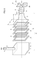
一方、流体案内部20は、図1及び図6に示すように、流体を放電電極部18に対して均一に供給する整流構造を有する。整流構造は、ベルマウス部72と、整流網部74と、流体流入ケース76とを有する。
ベルマウス部72は、放電電極部18の上流側に設置され、流路面積が流体の流通方向に向かって徐々に小さくなるベルマウス構造を有する。
整流網部74は、ベルマウス部72の上流側に設置され、1以上の整流網78と、整流網78を両側(上流側及び下流側)から押さえる押さえ枠80とを有する。整流網78の開口率は10~45%が望ましいが、ベルマウス部72の開口面積によっては、それよりも開口率が低くてもよい。その理由は、整流網部74は流体流入ケース76に入ってくるさまざまな速度ベクトルを有する流体を均一にベルマウス部72に送り込む役割を果たす。メッシュ数が大きく、開口率が低い方が望ましい。但し、ベルマウス部72の開口径が例えば30mmと大きな場合は、市販されているメッシュであれば、どれほど開口率が低くても問題はない。後述する導管82の内径が例えば6mmであれば、ベルマウス部72の開口径が30mmであれば、ベルマウス部72の開口面積は、導管82の開口面積の25倍になる。従って、開口率4%としても圧損は生じない。
流体流入ケース76は、整流網部74の上流側に設置され、ベルマウス部72への流体導出方向の内寸Daが、流体流量と正の相関関係を有する。内寸Daは、流体流量が10~20リットル/minの範囲において、20mm~100mmである。
流体流入ケース76への流体の供給方向は、ベルマウス部72への流体導出方向と異なる。すなわち、流体流入ケース76への流体の供給は、流体流入ケース76の1つの面に設けられた導管82を通じて行われ、流体の供給方向mと流体導出方向nとのなす角は80°~100°である。図6の例では、流体流入ケース76の複数の面のうち、ベルマウス部72への流体導出方向nと平行な面(例えば上面)に導管82が設けられ、流体の供給方向mと流体導出方向nとのなす角は略90°である。
ノズル24は、流路面積が流体の流通方向に向かって徐々に小さくなるベルマウス構造を有する第1ノズル24Aを用いてもよいし、角筒状の第2ノズル24Bを用いてもよい。第1ノズル24Aを用いることで、放電電極部18にて生成された励起物を含む流体を均一に被処理物22(図1参照)に当てることができる。
このように、本実施の形態に係るプラズマ処理装置12は、陽極と陰極とを有し、パルス電源14からの高電圧パルスの供給に基づいて陽極と陰極間に放電を発生させる放電電極部18と、放電電極部18に流体を案内する流体案内部20と、放電電極部18での放電によって流体内に発生した少なくとも励起種を被処理物22に噴射するノズル24と、を有し、流体案内部20及びノズル24のうち、少なくとも1つは、流路面積が流体の流通方向に向かって徐々に小さくなる構造を有するようにしたので、放電電極部18に対して流体を均一に流すことが可能で、放電電極部18において効率よくプラズマを発生させることができる。従って、プラズマの発生による励起物を間接的に被処理物22に当てて殺菌処理を行う場合に、殺菌処理の効率化を図ることができる。
ところで、第1放電電極26A及び第2放電電極26Bを作製する場合は、ゲルキャスト法を用いることが好ましい。ゲルキャスト法では、金型内に、第1導体30Aをセットし、セラミック粉末、分散媒、及びゲル化剤を含むスラリーを注型した後に、このスラリーを温度条件や架橋剤の添加等によりゲル化させることにより固化し、成形して、その後、焼成することで、第1放電電極26Aを作製する。第2放電電極26Bも同様の方法により、作製することができる。このゲルキャスト法によれば、スラリーの低粘度状態を介して第1導体30Aと混合させるため、混合後に空隙が残存しにくい。そのため、成形後に、焼成を行って第1放電電極26Aを作製しても、第1セラミック層34Aは緻密な状態が保たれる。第2セラミック層34Bにおいても同様である。
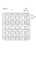
上述の例では、第1電極部36A及び第2電極部36Bをそれぞれくし歯状にした例を示したが、その他、図7の第1変形例に示すように、それぞれ格子状にし、第1導体30A及び第2導体30Bを共に格子状に形成してもよい。この場合、放電電極部18に対する流体の流通方向から見たときに、第1電極部36A(第1導体30A)と第2電極部36B(第2導体30B)とが交差した状態、すなわち、第1電極部36Aの開口に第2電極部36Bの交差部が位置する状態に設置する。
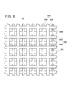
また、図8の第2変形例に示すように、第1電極部36A及び第2電極部36Bをそれぞれ格子状とし、第1電極部36A内の第1導体30Aと第2電極部36B内の第2導体30Bとをそれぞれくし歯状にしてもよい。
すなわち、第1電極部36Aの第1セラミック層34Aを格子状に構成し、第1セラミック層34A内の第1導体30Aを例えばx方向に延ばし、且つ、y方向に配列する。第2電極部36Bの第2セラミック層34Bを格子状に構成し、第2セラミック層34B内の第2導体30Bを例えばy方向に延ばし、且つ、x方向に配列する。
この場合、第1導体30A及び第2導体30Bを共に格子状にした場合と比して、電界強度の低下を抑制することができる。
上述した第2変形例において、第1セラミック層34Aのうち、第1導体30Aが内層されていない第1部分84A(y方向に延び、且つ、x方向に配列された部分)は、第1導体30Aと第1セラミック層34Aとからなる第1電極部36A間の強度を維持できる程度でよい。同様に、第2セラミック層34Bのうち、第2導体30Bが内層されていない第2部分84B(x方向に延び、且つ、y方向に配列された部分)は、第2導体30Bと第2セラミック層34Bとからなる第2電極部36B間の強度を維持できる程度でよい。
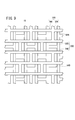
従って、図9の第3変形例に示すように、第1セラミック層34Aのうち、第1導体30Aが内層されていない第1部分84Aを間引きし、同様に、第2セラミック層34Bのうち、第2導体30Bが内層されていない第2部分84Bを間引きしてもよい。図9の例では上述の第1部分84A及び第2部分84Bをそれぞれ1本ずつ間引きした場合を示す。もちろん、第1電極部36A間の強度及び第2電極部36B間の強度を維持できる程度であれば、2本ずつ~数本ずつ間引きしてもよい。
[第1実施例]
実施例1~6、参考例1及び2について、整流網部74の開口率の違いによる放電電極部18での窒素の発光領域の変化を確認した。
実施例1~6、参考例1及び2について、整流網部74の開口率の違いによる放電電極部18での窒素の発光領域の変化を確認した。
<測定条件>
流体(窒素N2)の供給流量、プラズマ処理装置12の寸法は以下の通りである。
流体(窒素N2)の供給流量:10リットル/min
プラズマ処理装置12の寸法(図6参照):
導管82の内径:6mm
流体流入ケース76の流体導出方向の内寸Da:100mm
整流網78の枚数:2枚
ベルマウス部72:
軸方向の長さLa:104~124mm
整流網部74側の開口の一辺の長さLb:217mm
ノズル24側の開口の一辺の長さLc:61mm
パルス電源14:
パルス波形:DBD(誘電体バリア放電)タイプ
パルス周波数:2kpps
ピーク電圧値:16kV
ピーク電流値:3A
流体(窒素N2)の供給流量、プラズマ処理装置12の寸法は以下の通りである。
流体(窒素N2)の供給流量:10リットル/min
プラズマ処理装置12の寸法(図6参照):
導管82の内径:6mm
流体流入ケース76の流体導出方向の内寸Da:100mm
整流網78の枚数:2枚
ベルマウス部72:
軸方向の長さLa:104~124mm
整流網部74側の開口の一辺の長さLb:217mm
ノズル24側の開口の一辺の長さLc:61mm
パルス電源14:
パルス波形:DBD(誘電体バリア放電)タイプ
パルス周波数:2kpps
ピーク電圧値:16kV
ピーク電流値:3A
<発光領域の確認>
発光領域の確認は、ノズル24に向かってCCDカメラを設置し、露出する放電電極部18での放電の発生状態を撮像した。撮像した画像のうち、第1電極部36Aと第2電極部36Bが交差している部分全域に対する窒素の発光領域(N2発光領域と記す)の割合をパーセンテージで求めた。比較のために、図10Aに、N2発光領域100%の状態を示し、図10Bに、N2発光領域50%の状態を示す。
発光領域の確認は、ノズル24に向かってCCDカメラを設置し、露出する放電電極部18での放電の発生状態を撮像した。撮像した画像のうち、第1電極部36Aと第2電極部36Bが交差している部分全域に対する窒素の発光領域(N2発光領域と記す)の割合をパーセンテージで求めた。比較のために、図10Aに、N2発光領域100%の状態を示し、図10Bに、N2発光領域50%の状態を示す。
(実施例1~6)
実施例1、2、3、4、5、6は、整流網部74の開口率をそれぞれ16%、21%、23%、28%、37%、41%とした。
実施例1、2、3、4、5、6は、整流網部74の開口率をそれぞれ16%、21%、23%、28%、37%、41%とした。
(参考例1及び2)
参考例1、2は、整流網部74の開口率をそれぞれ5%、52%とした。
参考例1、2は、整流網部74の開口率をそれぞれ5%、52%とした。
<評価>
評価結果を下記表1に示す。
評価結果を下記表1に示す。

表1から、参考例1及び2のN2発光領域は50%であったが、実施例1~6は、いずれもN2発光領域が70%以上であり、良好であった。特に、実施例1~3は、N2発光領域は100%であった。このことから、整流網部74の開口率が小さいほど、流体の整流性が向上し、放電電極部18全域にわたって放電が安定に行われていることがわかる。但し、参考例1のように、極端に開口率が小さくなると、流体の整流性が悪くなり、放電が不安定になる。従って、整流網部74の開口率の好ましい範囲として、16%~41%が好ましく、さらに好ましくは16%~23%であることがわかる。
[第2実施例]
実施例11~15、参考例11~13について、流体流入ケース76の流体導出方向の内寸Daの違いによる放電電極部18での窒素の発光領域の変化を確認した。
実施例11~15、参考例11~13について、流体流入ケース76の流体導出方向の内寸Daの違いによる放電電極部18での窒素の発光領域の変化を確認した。
測定条件及び発光領域の確認は、上述した第1実施例と同じであるが、整流網部74の開口率を23%とした。
(実施例11~13)
実施例11、12、13は、流体流入ケース76の流体導出方向の内寸Daをそれぞれ30mm、60mm、100mmとし、流体流量をそれぞれ10(リットル/min)とした。
実施例11、12、13は、流体流入ケース76の流体導出方向の内寸Daをそれぞれ30mm、60mm、100mmとし、流体流量をそれぞれ10(リットル/min)とした。
(実施例14、15)
実施例14、15は、流体流入ケース76の流体導出方向の内寸Daをそれぞれ60mm、100mmとし、流体流量をそれぞれ20(リットル/min)とした。
実施例14、15は、流体流入ケース76の流体導出方向の内寸Daをそれぞれ60mm、100mmとし、流体流量をそれぞれ20(リットル/min)とした。
(参考例11、12、13)
参考例11、12、13は、流体流入ケース76の流体導出方向の内寸Daをそれぞれ10mm、10mm、30mmとし、流体流量をそれぞれ10(リットル/min)、20(リットル/min)、20(リットル/min)とした。
参考例11、12、13は、流体流入ケース76の流体導出方向の内寸Daをそれぞれ10mm、10mm、30mmとし、流体流量をそれぞれ10(リットル/min)、20(リットル/min)、20(リットル/min)とした。
<評価>
評価結果を下記表2に示す。
評価結果を下記表2に示す。
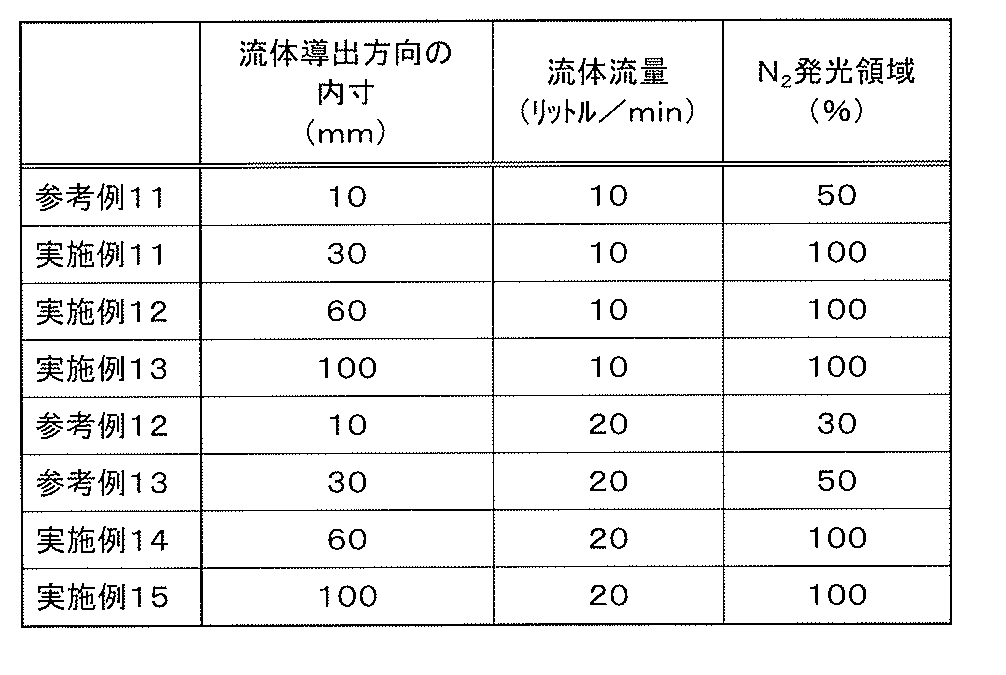
表2から、参考例12のN2発光領域は30%、参考例11及び13のN2発光領域は50%であったが、実施例11~15は、いずれもN2発光領域が100%であり、良好であった。このことから、流体流入ケース76の流体導出方向の内寸Daは大きい方が流体の整流性が良好になり、流量が大きいと内寸Daも大きくする必要があることがわかる。従って、流量毎に流体流入ケース76の流体導出方向の内寸Daの下限値が存在し、10リットル/minでは30mm、20リットル/minでは60mmが下限値である。
[第3実施例]
実施例21~28、参考例21~24について、放電電極部18を構成する陽極(第1電極部36A)の配列ピッチPaの違いによる放電電極部18での窒素の発光領域の変化を確認した。
実施例21~28、参考例21~24について、放電電極部18を構成する陽極(第1電極部36A)の配列ピッチPaの違いによる放電電極部18での窒素の発光領域の変化を確認した。
測定条件及び発光領域の確認は、上述した第1実施例と同じであるが、整流網部74の開口率を23%とした。
(実施例21~23)
実施例21、22、23は、陽極の配列ピッチPaをそれぞれ3mm、6mm、10mmとし、陽極と陰極間の距離dcをそれぞれ5mmとした。
実施例21、22、23は、陽極の配列ピッチPaをそれぞれ3mm、6mm、10mmとし、陽極と陰極間の距離dcをそれぞれ5mmとした。
(実施例24~26)
実施例24、25、26は、陽極の配列ピッチPaをそれぞれ30mm、40mm、50mmとし、陽極と陰極間の距離dcをそれぞれ40mmとした。
実施例24、25、26は、陽極の配列ピッチPaをそれぞれ30mm、40mm、50mmとし、陽極と陰極間の距離dcをそれぞれ40mmとした。
(実施例27、28)
実施例27、28は、陽極の配列ピッチPaをそれぞれ50mm、80mmとし、陽極と陰極間の距離dcをそれぞれ100mmとした。
実施例27、28は、陽極の配列ピッチPaをそれぞれ50mm、80mmとし、陽極と陰極間の距離dcをそれぞれ100mmとした。
(参考例21~24)
参考例21、22、23、24は、陽極の配列ピッチPaをそれぞれ2mm、20mm、40mm、100mmとし、陽極と陰極間の距離dcをそれぞれ5mm、40mm、100mm、100mmとした。
参考例21、22、23、24は、陽極の配列ピッチPaをそれぞれ2mm、20mm、40mm、100mmとし、陽極と陰極間の距離dcをそれぞれ5mm、40mm、100mm、100mmとした。
<評価>
評価結果を下記表3に示す。
評価結果を下記表3に示す。
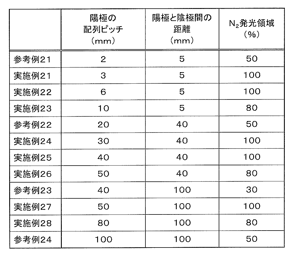
表3から、参考例21、22、24のN2発光領域は50%、参考例23のN2発光領域は30%であったが、実施例21~28は、いずれもN2発光領域が80%以上であり、良好であった。特に、実施例21、22、24、25、27は、N2発光領域は100%であった。また、実験結果から、陽極と陰極間の距離dcが広くなるほど陽極の配列ピッチPaも広くしないと中央部の放電が弱くなることがわかった。一方、陽極の配列ピッチPaが広すぎてもプラズマにコールドスポット領域ができ、効率が低下することがわかった。従って、陽極の配列ピッチPaは陽極と陰極間の距離dcの50%~100%にすることが望ましい。
[第4実施例]
実施例31~36、参考例31及び32について、放電電極部18を構成する第1セラミック層34Aの気孔寸法の違いによる放電電極部18の耐久時間を確認した。気孔はX線CT(コンピュータ断層撮影)による非破壊観察画像で確認した。耐久時間は、実験の開始時点から絶縁破壊が生じるまでの時間である。図11に、第1セラミック層34A中に径が50μmの気孔が存在している状態を示す。この図11は、X線CTによる非破壊観察画像である。
実施例31~36、参考例31及び32について、放電電極部18を構成する第1セラミック層34Aの気孔寸法の違いによる放電電極部18の耐久時間を確認した。気孔はX線CT(コンピュータ断層撮影)による非破壊観察画像で確認した。耐久時間は、実験の開始時点から絶縁破壊が生じるまでの時間である。図11に、第1セラミック層34A中に径が50μmの気孔が存在している状態を示す。この図11は、X線CTによる非破壊観察画像である。
(実施例31~36)
実施例31、32、33、34、35、36は、第1セラミック層34Aに存在する気孔の寸法が30μm、30μm、20μm、15μm、15μm、10μmである。
実施例31、32、33、34、35、36は、第1セラミック層34Aに存在する気孔の寸法が30μm、30μm、20μm、15μm、15μm、10μmである。
(参考例31、32)
参考例31、32は、第1セラミック層34Aに存在する気孔の寸法が50μm、70μmである。
参考例31、32は、第1セラミック層34Aに存在する気孔の寸法が50μm、70μmである。
<評価>
評価結果を下記表4に示す。
評価結果を下記表4に示す。
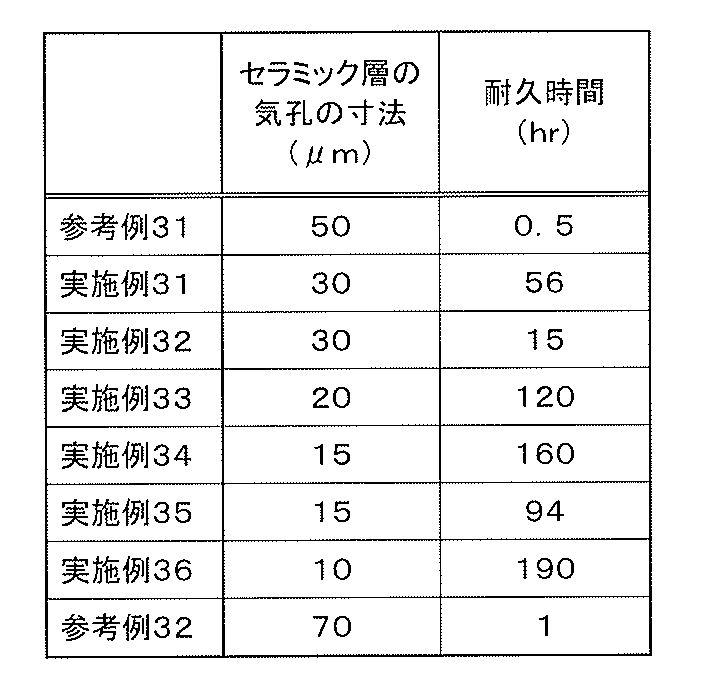
表4から、気孔の寸法が小さくなるほど耐久時間が長くなる傾向があることがわかる。また、実験結果から、気孔は大きいものが1個でもあると絶縁破壊はそこから起こり、数値上の気孔率が0%であっても破損することがわかった。セラミック層の厚みが200μmの場合、φ40μmの気孔があると、実質の材料厚みが20%も低下したことに相当する。従って、気孔の大きさを極力小さくすることが重要となり、第1セラミック層34A及び第2セラミック層34Bの内部に50μm以上の気孔を有しないことが望ましいことがわかる。
[第5実施例]
実施例41~46、参考例41及び42について、放電電極部18を構成する第1導体30Aと第1セラミック層34Aの断面積比(第1導体30Aの断面積Aa1/第1セラミック層34Aの断面積Ab1)の違いによるプラズマ発光強度の変化を確認した。プラズマ発光強度は電極近傍におけるN2分子からの発光(337.1nm)強度を発光分光計(OES)により測定した。
実施例41~46、参考例41及び42について、放電電極部18を構成する第1導体30Aと第1セラミック層34Aの断面積比(第1導体30Aの断面積Aa1/第1セラミック層34Aの断面積Ab1)の違いによるプラズマ発光強度の変化を確認した。プラズマ発光強度は電極近傍におけるN2分子からの発光(337.1nm)強度を発光分光計(OES)により測定した。
(実施例41~46)
実施例41、42、43、44、45、46は、それぞれ断面積比(Aa1/Ab1)が0.15、0.3、0.5、0.7、0.8、0.9である。
実施例41、42、43、44、45、46は、それぞれ断面積比(Aa1/Ab1)が0.15、0.3、0.5、0.7、0.8、0.9である。
(参考例41及び42)
参考例41、42は、それぞれ断面積比(Aa1/Ab1)が0.05、1.5である。
参考例41、42は、それぞれ断面積比(Aa1/Ab1)が0.05、1.5である。
<評価>
評価結果を下記表5に示す。
評価結果を下記表5に示す。
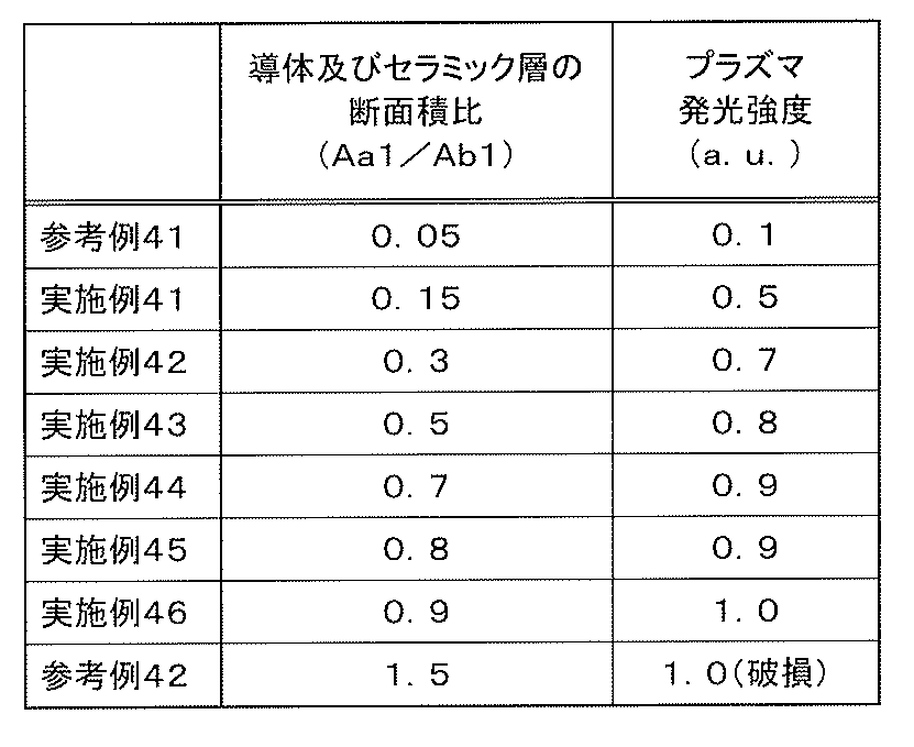
表5から、参考例41のプラズマ発光強度は0.1であったが、実施例41~46は、いずれもプラズマ発光強度が0.5以上であり、良好であった。特に、実施例44、45、46はプラズマ発光強度が0.9、0.9、1.0であった。一方、参考例42は、プラズマ発光強度が1.0であったが破損していた。このことから、第1セラミック層34Aの断面積が小さいほど第1導体30Aの表面にかかる電圧は高くなり、プラズマ発光強度が大きくなることがわかる。しかし、第1セラミック層34Aを薄くしすぎると、絶縁破壊が起こりやすくなり、小さな気孔でも大きな電界集中を招き破損しやすくなる。従って、断面積比(Aa1/Ab1)は、0.1<Aa1/Ab1<1.0であることがわかる。
[第6実施例]
上述した第5実施例と同様に、実施例51~56、参考例51及び52について、放電電極部18を構成する第2導体30Bと第2セラミック層34Bの断面積比(第2導体30Bの断面積Aa2/第2セラミック層34Bの断面積Ab2)の違いによるプラズマ発光強度の変化を確認した。
上述した第5実施例と同様に、実施例51~56、参考例51及び52について、放電電極部18を構成する第2導体30Bと第2セラミック層34Bの断面積比(第2導体30Bの断面積Aa2/第2セラミック層34Bの断面積Ab2)の違いによるプラズマ発光強度の変化を確認した。
(実施例51~56)
実施例51、52、53、54、55、56は、それぞれ断面積比(Aa2/Ab2)が0.1、0.5、1.0、1.3、1.5、1.8である。
実施例51、52、53、54、55、56は、それぞれ断面積比(Aa2/Ab2)が0.1、0.5、1.0、1.3、1.5、1.8である。
(参考例51及び52)
参考例51、52は、それぞれ断面積比(Aa2/Ab2)が0.05、2.5である。
参考例51、52は、それぞれ断面積比(Aa2/Ab2)が0.05、2.5である。
<評価>
評価結果を下記表6に示す。
評価結果を下記表6に示す。
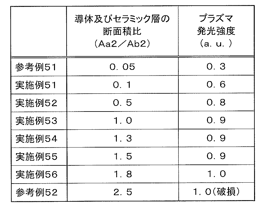
表6から、参考例51のプラズマ発光強度は0.3であったが、実施例51~56は、いずれもプラズマ発光強度が0.6以上であり、良好であった。特に、実施例53、54、55、56はプラズマ発光強度が0.9、0.9、0.9、1.0であった。一方、参考例52は、プラズマ発光強度が1.0であったが破損していた。このことから、上述した第5実施例と同様に、第2セラミック層34Bの断面積が小さいほど第2導体30Bの表面にかかる電圧は高くなり、プラズマ発光強度が大きくなることがわかる。しかし、第2セラミック層34Bを薄くしすぎると、絶縁破壊が起こりやすくなり、小さな気孔でも大きな電界集中を招き破損しやすくなる。従って、断面積比(Aa2/Ab2)は、0.08<Aa2/Ab2<2.0であることがわかる。
[第7実施例]
実施例61~66、参考例61及び62について、放電電極部18を構成する第1導体30A(陽極導体)の直径の違いによるプラズマ発光強度の変化を確認した。
実施例61~66、参考例61及び62について、放電電極部18を構成する第1導体30A(陽極導体)の直径の違いによるプラズマ発光強度の変化を確認した。
(実施例61~66)
実施例61、62、63、64、65、66は、第1導体30Aの直径d1がそれぞれ200μm、300μm、500μm、800μm、900μm、1000μmである。
実施例61、62、63、64、65、66は、第1導体30Aの直径d1がそれぞれ200μm、300μm、500μm、800μm、900μm、1000μmである。
(参考例61及び62)
参考例61、62は、第1導体30Aの直径d1がそれぞれ100μm、1200μmである。
参考例61、62は、第1導体30Aの直径d1がそれぞれ100μm、1200μmである。
<評価>
評価結果を下記表7に示す。
評価結果を下記表7に示す。
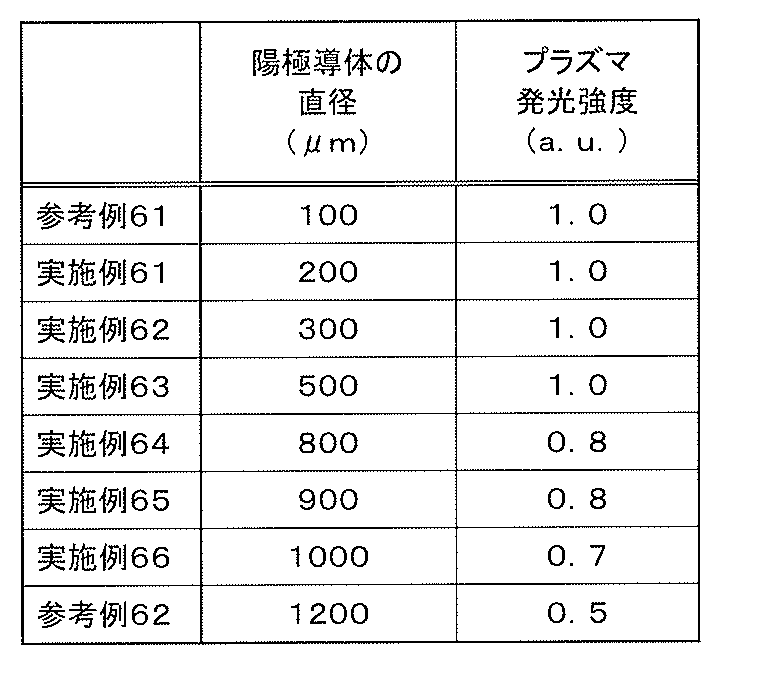
表7から、第1導体30Aの直径d1は小さいほど高い電界強度がかかり、高エネルギー電子の割合が増え、プラズマからの活性種発生数が増大することがわかる。反面、線材が切れ易くなりプラズマ処理装置の信頼性が低下する。参考例61は、プラズマ発光強度が1.0であったが、信頼性の点で不安がある。従って、第1導体30Aの直径d1は、200~1000μmが好ましく、さらに好ましくは300~500μmである。
なお、本発明に係る殺菌装置は、上述の実施の形態に限らず、本発明の要旨を逸脱することなく、種々の構成を採り得ることはもちろんである。
Claims (18)
- パルス電源(14)からの高電圧パルスによる放電によって発生したプラズマを利用して対象物(22)の少なくとも表面を殺菌する殺菌装置において、
陽極と陰極とを有し、前記パルス電源(14)からの前記高電圧パルスの供給に基づいて前記陽極と前記陰極間に放電を発生させる放電電極部(18)と、
前記放電電極部(18)に流体を案内する流体案内部(20)と、
前記放電電極部(18)を通過した前記流体を前記対象物(22)に向けて出力するノズル(24)と、を有し、
前記放電電極部(18)に前記流体を導入しながら、前記放電電極部(18)において前記放電によりプラズマを発生させ、その励起物を前記流体と共に前記対象物(22)に当て、
前記流体案内部(20)及び前記ノズル(24)のうち、少なくとも1つは、流路面積が前記流体の流通方向に向かって徐々に小さくなる構造を有することを特徴とする殺菌装置。 - 請求項1記載の殺菌装置において、
前記流体案内部(20)は、前記流体を前記放電電極部(18)に対して均一に供給する整流構造を有することを特徴とする殺菌装置。 - 請求項2記載の殺菌装置において、
前記整流構造は、
流路面積が前記流体の流通方向に向かって徐々に小さくなるベルマウス構造(72)と、
前記ベルマウス構造(72)の上流側に設置された1以上の整流網(78)と、
前記ベルマウス構造(72)への流体導出方向の内寸が流体流量と正の相関関係にある流体流入ケース(76)と、を有することを特徴とする殺菌装置。 - 請求項3記載の殺菌装置において、
前記整流網(78)の開口率が10~45%であることを特徴とする殺菌装置。 - 請求項3記載の殺菌装置において、
前記流体流入ケース(76)の前記ベルマウス構造(72)への流体導入方向の内寸は、流体流量10リットル/minから20リットル/minにおいて20mm~100mmであることを特徴とする殺菌装置。 - 請求項3記載の殺菌装置において、
前記流体案内部(20)への前記流体の供給方向が、前記放電電極部(18)への前記流体の流通方向と異なることを特徴とする殺菌装置。 - 請求項6記載の殺菌装置において、
前記流体の供給方向と前記流体の流通方向とのなす角が80°~100°であることを特徴とする殺菌装置。 - 請求項1記載の殺菌装置において、
前記ノズル(24)は、流路面積が前記流体の流通方向に向かって徐々に小さくなる構造を有することを特徴とする殺菌装置。 - 請求項1記載の殺菌装置において、
前記放電電極部(18)は、前記陽極となる第1放電電極(26A)と、前記陰極となる第2放電電極(26B)とを有し、
前記第1放電電極(26A)を構成する複数の第1導体(30A)と、前記第2放電電極(26B)を構成する複数の第2導体(30B)とが、互いに離間し、且つ、前記放電電極部(18)に対する前記流体の流通方向から見たときに、前記第1導体(30A)と前記第2導体(30B)とが交差した位置関係にあることを特徴とする殺菌装置。 - 請求項1記載の殺菌装置において、
前記放電電極部(18)は、前記陽極となる第1放電電極(26A)と、前記陰極となる第2放電電極(26B)とを有し、
前記第1放電電極(26A)を構成する複数の第1導体(30A)と、前記第2放電電極(26B)を構成する複数の第2導体(30B)とが、ねじれの位置関係にあることを特徴とする殺菌装置。 - 請求項10記載の殺菌装置において、
前記放電電極部818)に対する前記流体の流通方向から見たときに、前記第1導体(30A)と前記第2導体(30B)とで複数の格子が形成されることを特徴とする殺菌装置。 - 請求項10記載の殺菌装置において、
前記第1導体(30A)と前記第2導体(30B)との交差部分の配列ピッチが5~50mmであることを特徴とする殺菌装置。 - 請求項10記載の殺菌装置において、
前記放電電極部(18)に対する前記流体の流通方向から見たときに、前記放電電極部(18)の開口率が30~50%であることを特徴とする殺菌装置。 - 請求項10記載の殺菌装置において、
前記第1放電電極(26A)は、前記第1導体(30A)と、該第1導体(30A)を被覆する第1セラミック層(34A)とを有し、
前記第2放電電極(26B)は、前記第2導体(30B)と、該第2導体(30B)を被覆する第2セラミック層(34B)とを有することを特徴とする殺菌装置。 - 請求項14記載の殺菌装置において、
前記第1セラミック層(34A)及び前記第2セラミック層(34B)の内部に50μm以上の気孔を有しないことを特徴とする殺菌装置。 - 請求項14記載の殺菌装置において、
前記第1導体(30A)と前記第1セラミック層(34A)を、軸方向に直交する方向に切断した断面において、前記第1導体(30A)の面積をAa1、前記第1セラミック層(34A)の面積をAb1とし、
前記第2導体(30B)と前記第2セラミック層(34B)を、軸方向に直交する方向に切断した断面において、前記第2導体(30B)の面積をAa2、前記第2セラミック層(34B)の面積をAb2としたとき、
0.1<Aa1/Ab1<1.0
0.08<Aa2/Ab2<2.0
であることを特徴とする殺菌装置。 - 請求項16記載の殺菌装置において、
前記第1導体(30A)及び前記第2導体(30B)の各直径が200~1000μmであることを特徴とする殺菌装置。 - 請求項1記載の殺菌装置において、
前記パルス電源(14)は、前記陽極及び前記陰極間に前記高電圧パルスを印加するパルス発生部(41)と、前記陽極及び前記陰極間に放電を発生させるように前記パルス発生部(41)を制御するパルス制御部(42)とを有し、
前記パルス発生部(41)は、直流電源部(46)の両端に直列接続されたトランス(47)及びスイッチ(54)を有し、前記パルス制御部(42)の前記スイッチ(54)に対するオン制御によって前記トランス(47)への誘導エネルギーの蓄積を行い、前記パルス制御部(42)の前記スイッチ(54)に対するオフ制御によって前記トランス(47)の二次側での前記高電圧パルスの発生を行うパルス発生回路(43)を有することを特徴とする殺菌装置。
Priority Applications (1)
| Application Number | Priority Date | Filing Date | Title |
|---|---|---|---|
| JP2015512364A JP6513020B2 (ja) | 2013-04-15 | 2014-03-18 | 殺菌装置 |
Applications Claiming Priority (2)
| Application Number | Priority Date | Filing Date | Title |
|---|---|---|---|
| JP2013-085297 | 2013-04-15 | ||
| JP2013085297 | 2013-04-15 |
Publications (1)
| Publication Number | Publication Date |
|---|---|
| WO2014171248A1 true WO2014171248A1 (ja) | 2014-10-23 |
Family
ID=51731205
Family Applications (1)
| Application Number | Title | Priority Date | Filing Date |
|---|---|---|---|
| PCT/JP2014/057226 Ceased WO2014171248A1 (ja) | 2013-04-15 | 2014-03-18 | 殺菌装置 |
Country Status (2)
| Country | Link |
|---|---|
| JP (1) | JP6513020B2 (ja) |
| WO (1) | WO2014171248A1 (ja) |
Cited By (6)
| Publication number | Priority date | Publication date | Assignee | Title |
|---|---|---|---|---|
| JP2017016814A (ja) * | 2015-06-30 | 2017-01-19 | ダイハツ工業株式会社 | プラズマ発生用電極、電極パネルおよびプラズマリアクタ |
| JP2017094263A (ja) * | 2015-11-24 | 2017-06-01 | 日本特殊陶業株式会社 | プラズマリアクタ |
| JP2018035023A (ja) * | 2016-08-30 | 2018-03-08 | 株式会社デンソー | ガス改質装置 |
| JPWO2019035314A1 (ja) * | 2017-08-14 | 2020-03-26 | 株式会社Kokusai Electric | プラズマ異常判定方法、半導体装置の製造方法及び基板処理装置 |
| WO2021239901A1 (en) * | 2020-05-29 | 2021-12-02 | Robert Bosch Gmbh | Atmospheric-pressure plasma cleaning apparatus |
| US12702271B2 (en) | 2021-04-27 | 2026-08-11 | Sony Group Corporation | Medical imaging system and imaging device |
Citations (5)
| Publication number | Priority date | Publication date | Assignee | Title |
|---|---|---|---|---|
| JPH11342181A (ja) * | 1998-06-03 | 1999-12-14 | Mitsubishi Electric Corp | 負イオン発生装置 |
| JP2001145689A (ja) * | 1999-11-24 | 2001-05-29 | Matsushita Electric Works Ltd | プラズマ滅菌処理装置及びプラズマ滅菌処理方法 |
| JP2010530115A (ja) * | 2007-05-15 | 2010-09-02 | マックス―プランク―ゲゼエルシャフト ツール フェルデルング デル ヴィッセンシャフテン エー.ヴェー | プラズマ源 |
| JP2012079429A (ja) * | 2010-09-30 | 2012-04-19 | Ngk Insulators Ltd | プラズマ処理装置 |
| JP2012252843A (ja) * | 2011-06-01 | 2012-12-20 | Kazuo Shimizu | 表面活性化処理装置 |
-
2014
- 2014-03-18 JP JP2015512364A patent/JP6513020B2/ja not_active Expired - Fee Related
- 2014-03-18 WO PCT/JP2014/057226 patent/WO2014171248A1/ja not_active Ceased
Patent Citations (5)
| Publication number | Priority date | Publication date | Assignee | Title |
|---|---|---|---|---|
| JPH11342181A (ja) * | 1998-06-03 | 1999-12-14 | Mitsubishi Electric Corp | 負イオン発生装置 |
| JP2001145689A (ja) * | 1999-11-24 | 2001-05-29 | Matsushita Electric Works Ltd | プラズマ滅菌処理装置及びプラズマ滅菌処理方法 |
| JP2010530115A (ja) * | 2007-05-15 | 2010-09-02 | マックス―プランク―ゲゼエルシャフト ツール フェルデルング デル ヴィッセンシャフテン エー.ヴェー | プラズマ源 |
| JP2012079429A (ja) * | 2010-09-30 | 2012-04-19 | Ngk Insulators Ltd | プラズマ処理装置 |
| JP2012252843A (ja) * | 2011-06-01 | 2012-12-20 | Kazuo Shimizu | 表面活性化処理装置 |
Cited By (8)
| Publication number | Priority date | Publication date | Assignee | Title |
|---|---|---|---|---|
| JP2017016814A (ja) * | 2015-06-30 | 2017-01-19 | ダイハツ工業株式会社 | プラズマ発生用電極、電極パネルおよびプラズマリアクタ |
| JP2017094263A (ja) * | 2015-11-24 | 2017-06-01 | 日本特殊陶業株式会社 | プラズマリアクタ |
| WO2017090677A1 (ja) * | 2015-11-24 | 2017-06-01 | 日本特殊陶業株式会社 | プラズマリアクタ |
| EP3383144A4 (en) * | 2015-11-24 | 2019-05-08 | NGK Spark Plug Co., Ltd. | PLASMA REACTOR |
| JP2018035023A (ja) * | 2016-08-30 | 2018-03-08 | 株式会社デンソー | ガス改質装置 |
| JPWO2019035314A1 (ja) * | 2017-08-14 | 2020-03-26 | 株式会社Kokusai Electric | プラズマ異常判定方法、半導体装置の製造方法及び基板処理装置 |
| WO2021239901A1 (en) * | 2020-05-29 | 2021-12-02 | Robert Bosch Gmbh | Atmospheric-pressure plasma cleaning apparatus |
| US12702271B2 (en) | 2021-04-27 | 2026-08-11 | Sony Group Corporation | Medical imaging system and imaging device |
Also Published As
| Publication number | Publication date |
|---|---|
| JPWO2014171248A1 (ja) | 2017-02-23 |
| JP6513020B2 (ja) | 2019-05-15 |
Similar Documents
| Publication | Publication Date | Title |
|---|---|---|
| JP6513020B2 (ja) | 殺菌装置 | |
| EP2849204B1 (de) | Plasmaerzeugungsvorrichtung | |
| KR101544329B1 (ko) | 플라즈마 발생 장치, cvd 장치 및 플라즈마 처리 입자 생성 장치 | |
| CN104981270B (zh) | 采用低压等离子体处理生物组织的设备和方法 | |
| CN104736087B (zh) | 用于通过低压等离子体处理生物组织的设备和方法 | |
| JP2015144982A (ja) | プラズマ処理方法 | |
| JP2020509539A5 (ja) | ||
| WO2010107722A1 (en) | Tubular floating electrode dielectric barrier discharge for applications in sterilization and tissue bonding | |
| CN103585650A (zh) | 一种低温等离子体内窥镜消毒装置及方法 | |
| WO2017198469A1 (de) | Schaltungsanordnung zur bereitstellung von hochfrequenzenergie und system zur erzeugung einer elektrischen entladung | |
| EP2809468B1 (en) | Spark ablation device and method for generating nanoparticles | |
| JP2010530115A (ja) | プラズマ源 | |
| WO2014077181A1 (ja) | 水処理装置および水処理方法 | |
| JPWO2011065171A1 (ja) | プラズマ処理装置 | |
| Joh et al. | Electrical and optical characterization of atmospheric-pressure helium plasma jets generated with a pin electrode: Effects of the electrode material, ground ring electrode, and nozzle shape | |
| CN107409464A (zh) | 等离子发生方法及杀菌水生成方法 | |
| CN104936371A (zh) | 一种空心电极介质阻挡结构 | |
| JP2012084396A (ja) | パルスパワー方式低温プラズマジェット発生装置 | |
| CN108781499B (zh) | 等离子发生装置 | |
| CN112004304B (zh) | 一种电晕复合介质阻挡放电等离子体射流发生装置 | |
| WO2019180839A1 (ja) | プラズマ装置、プラズマ生成方法 | |
| EP3134350B1 (de) | Vorrichtung zur photochemischen behandlung oder reinigung eines flüssigen mediums | |
| WO2014191012A1 (de) | Vorrichtung und verfahren zur behandlung eines drahts aus leitfähigem material | |
| KR101016478B1 (ko) | 에어로졸 하전 중화장치 | |
| JP6662252B2 (ja) | 流体浄化装置および流体浄化方法 |
Legal Events
| Date | Code | Title | Description |
|---|---|---|---|
| 121 | Ep: the epo has been informed by wipo that ep was designated in this application |
Ref document number: 14785551 Country of ref document: EP Kind code of ref document: A1 |
|
| ENP | Entry into the national phase |
Ref document number: 2015512364 Country of ref document: JP Kind code of ref document: A |
|
| NENP | Non-entry into the national phase |
Ref country code: DE |
|
| 122 | Ep: pct application non-entry in european phase |
Ref document number: 14785551 Country of ref document: EP Kind code of ref document: A1 |