WO2014157627A1 - Feuille de capteur capacitif et capteurs capacitifs - Google Patents
Feuille de capteur capacitif et capteurs capacitifs Download PDFInfo
- Publication number
- WO2014157627A1 WO2014157627A1 PCT/JP2014/059143 JP2014059143W WO2014157627A1 WO 2014157627 A1 WO2014157627 A1 WO 2014157627A1 JP 2014059143 W JP2014059143 W JP 2014059143W WO 2014157627 A1 WO2014157627 A1 WO 2014157627A1
- Authority
- WO
- WIPO (PCT)
- Prior art keywords
- electrode layer
- sensor sheet
- dielectric layer
- capacitive sensor
- layer
- Prior art date
Links
Images


Classifications
-
- G—PHYSICS
- G01—MEASURING; TESTING
- G01L—MEASURING FORCE, STRESS, TORQUE, WORK, MECHANICAL POWER, MECHANICAL EFFICIENCY, OR FLUID PRESSURE
- G01L1/00—Measuring force or stress, in general
- G01L1/14—Measuring force or stress, in general by measuring variations in capacitance or inductance of electrical elements, e.g. by measuring variations of frequency of electrical oscillators
- G01L1/142—Measuring force or stress, in general by measuring variations in capacitance or inductance of electrical elements, e.g. by measuring variations of frequency of electrical oscillators using capacitors
- G01L1/146—Measuring force or stress, in general by measuring variations in capacitance or inductance of electrical elements, e.g. by measuring variations of frequency of electrical oscillators using capacitors for measuring force distributions, e.g. using force arrays
-
- G—PHYSICS
- G01—MEASURING; TESTING
- G01B—MEASURING LENGTH, THICKNESS OR SIMILAR LINEAR DIMENSIONS; MEASURING ANGLES; MEASURING AREAS; MEASURING IRREGULARITIES OF SURFACES OR CONTOURS
- G01B1/00—Measuring instruments characterised by the selection of material therefor
-
- G—PHYSICS
- G01—MEASURING; TESTING
- G01B—MEASURING LENGTH, THICKNESS OR SIMILAR LINEAR DIMENSIONS; MEASURING ANGLES; MEASURING AREAS; MEASURING IRREGULARITIES OF SURFACES OR CONTOURS
- G01B7/00—Measuring arrangements characterised by the use of electric or magnetic techniques
- G01B7/16—Measuring arrangements characterised by the use of electric or magnetic techniques for measuring the deformation in a solid, e.g. by resistance strain gauge
- G01B7/22—Measuring arrangements characterised by the use of electric or magnetic techniques for measuring the deformation in a solid, e.g. by resistance strain gauge using change in capacitance
-
- G—PHYSICS
- G01—MEASURING; TESTING
- G01B—MEASURING LENGTH, THICKNESS OR SIMILAR LINEAR DIMENSIONS; MEASURING ANGLES; MEASURING AREAS; MEASURING IRREGULARITIES OF SURFACES OR CONTOURS
- G01B7/00—Measuring arrangements characterised by the use of electric or magnetic techniques
- G01B7/28—Measuring arrangements characterised by the use of electric or magnetic techniques for measuring contours or curvatures
Definitions
- the present invention uses a capacitance type sensor sheet, in particular, a capacitance type sensor sheet used for measuring at least one of a stretching deformation strain amount and a stretching deformation strain distribution, and the capacitance type sensor sheet.
- the present invention relates to a capacitance type sensor.
- the capacitance type sensor sheet can detect the uneven shape of the measurement object from the capacitance change between the pair of electrode layers, and can be used for sensors such as a surface pressure distribution sensor and a strain gauge.
- the capacitance (capacitance) in a capacitance type sensor is expressed by the following equation (1).
- C ⁇ 0 ⁇ r S / d (1)
- ⁇ 0 the permittivity of free space
- ⁇ r is the relative permittivity of the dielectric layer
- S is the electrode layer area
- d is the distance between the electrodes.
- a capacitive sensor sheet used as a surface pressure distribution sensor for example, a dielectric layer made of an elastomer, and a pair of electrode layers (a front side electrode and a back side electrode) formed including an elastomer and a conductive filler, And a pair of electrode layers formed so as to sandwich a dielectric layer is known (for example, see Patent Document 1).
- a sensor sheet has a characteristic that the change in capacitance is relatively large because the dielectric layer is made of an elastomer.
- the capacitive sensor sheet used in the conventional surface pressure distribution sensor the load distribution of the measurement object can be measured, but the deformation amount due to the load cannot be known.
- the sensor seat is attached to a flexible object such as a cushion and a load is applied to the sensor seat, it is not possible to measure how the cushion is deformed.
- the capacitance type sensor sheet used as the surface pressure distribution sensor usually has a dielectric layer displacement amount (elongation rate) of about several percent during measurement. For this reason, even a flexible dielectric layer has flexibility, but the elongation rate is about several percent.
- the displacement amount (elongation rate) of the dielectric layer at the time of measurement is 100%, depending on the use mode. It is not uncommon to exceed. For this reason, in a capacitive sensor sheet used for measuring the amount of stretch deformation strain and the distribution of stretch deformation strain, a high elongation rate is required for the dielectric layer.
- the electrode layer is required to be able to follow the dielectric layer when it is stretched and to maintain conductivity (electric resistance does not increase).
- the capacitance-type sensor sheet described in Patent Document 1 cannot sufficiently satisfy such a requirement, and the capacitance used for measurement of at least one of the amount of expansion / contraction deformation strain and the distribution of expansion / contraction deformation strain. It was difficult to use as a mold sensor sheet.
- the electrode layer is formed using a conductive filler such as carbon black, the conductive path is easily cut when the electrode layer is stretched along with the elongation of the dielectric layer, and the amount of stretch deformation strain and stretch deformation strain are increased. It could not be used to measure the distribution.
- the dielectric layer and the electrode layer have a high elongation rate, and the sensor sheet has a large expansion / contraction. Even when subjected to deformation or repeated deformation, it is required that the electrode layer and the dielectric layer are less likely to be peeled off, and that the electrode layer has low durability (such as increased electrical resistance) and has excellent durability. Is done.
- the present invention has been made in view of such circumstances, and the object thereof is to have a high elongation rate, to follow the deformation and operation of a flexible measurement object, and to perform elastic deformation and repetition.
- An object of the present invention is to provide a capacitive sensor sheet that is excellent in durability against deformation and can be used to measure at least one of the amount of stretch deformation strain and the strain distribution of stretch deformation.
- the capacitive sensor sheet of the present invention is A capacitance type sensor sheet used for measuring at least one of a stretching deformation strain amount and a stretching deformation strain distribution, A dielectric layer, a front electrode layer laminated on the surface of the dielectric layer, and a back electrode layer laminated on the back surface of the dielectric layer,
- the dielectric layer is made of an elastomer composition containing urethane rubber
- the said front side electrode layer and back side electrode layer consist of an electroconductive composition containing a carbon nanotube.
- the capacitance type sensor sheet has an elongation rate of 30% or more that can withstand uniaxial tension.
- the urethane rubber is preferably olefin urethane rubber or ester urethane rubber.
- the carbon nanotubes preferably have an average length of 100 ⁇ m or more and a purity of 99% by weight or more.
- the average thicknesses of the front electrode layer and the back electrode layer are 0.1 to 10 ⁇ m, respectively.
- the front electrode layer and the back electrode layer are each composed of a plurality of strips arranged in parallel, and the front electrode layer and the back electrode layer are arranged so as to intersect at a substantially right angle when viewed from the front and back directions. It is preferable.
- the capacitance type sensor of the present invention is a capacitance type sensor used for measuring at least one of a stretching deformation strain amount and a stretching deformation strain distribution, A capacitive sensor sheet of the present invention; Measuring means; Each of the said front side electrode layer and the said back side electrode layer, and the external wiring which connects the said measurement means are included.
- the capacitive sensor sheet of the present invention includes a dielectric layer made of urethane rubber and an electrode layer made of a conductive composition containing carbon nanotubes, it has a high elongation rate and is a flexible measuring object. It is possible to follow the deformation and movement of the material, has excellent measurement accuracy, and does not cause peeling between the dielectric layer and the electrode layer even during expansion and deformation, and is durable (long-term reliability) It is excellent and can be suitably used to measure at least one of the amount of stretch deformation strain and the strain distribution of stretch deformation.
- the electrostatic capacity type sensor sheet of the present invention can be used even if it is repeatedly used (for example, even if the expansion and contraction is repeated 1000 times). Excellent measurement accuracy can be maintained over a long period of time without changing (capacitance at no load).
- the capacitive sensor of the present invention includes the capacitive sensor sheet of the present invention, it measures at least one of the amount of expansion / contraction strain and the distribution of expansion / contraction strain excellent in measurement accuracy and durability (long-term reliability). It is a capacitance type sensor.
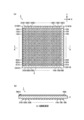
- (A) is a plan view schematically showing an example of the capacitive sensor sheet of the present invention
- (b) is a cross-sectional view taken along the line AA of the capacitive sensor sheet shown in (a).
- Evaluation 1 It is a graph which shows the measurement result which measured the change of the electrical resistance with respect to repeated deformation
- Evaluation 1 It is a graph which shows the measurement result which measured the change of the electrical resistance with respect to repeated deformation
- Evaluation 2 It is a graph which shows the measurement result which measured the change of the electrostatic capacitance with respect to deformation of a sensor sheet.
- Evaluation 2 It is a graph which shows the measurement result which measured the change of the electrostatic capacitance with respect to deformation of a sensor sheet.
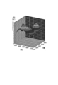
- 3 is a three-dimensional graph showing a stretch deformation strain distribution detected by a sensor sheet 1.
- Evaluation 3 A photograph showing the result of evaluating the adhesion between the dielectric layer and the electrode layer.
- FIG. 1A is a plan view schematically showing an example of the capacitive sensor sheet of the present invention
- FIG. 1B is an AA line of the capacitive sensor sheet shown in FIG. It is sectional drawing.
- a capacitive sensor sheet 1 of the present invention has a sheet-like dielectric layer 2 and a belt-like shape laminated on the surface (front surface) of the dielectric layer 2.
- the portions where the front-side electrode layer and the back-side electrode layer intersect in the front-back direction (thickness direction of the dielectric layer) are detection units C0101 to C1616. It should be noted that in the detection unit code “CXXX”, the upper two digits “XX” correspond to the front electrode layers 01A to 16A, and the lower two digits “ ⁇ ” indicate the back electrode layers 01B to 01B. Corresponding to 16B.
- the front electrode layers 01A to 16A each have a strip shape, and a total of 16 layers are laminated on the surface of the dielectric layer 2.
- the front-side electrode layers 01A to 16A each extend in the X direction (the left-right direction in FIG. 1A).
- the front-side electrode layers 01A to 16A are respectively arranged so as to be substantially parallel to each other at a predetermined interval in the Y direction (vertical direction in FIG. 1A).
- the back-side electrode layers 01B to 16B each have a strip shape, and a total of 16 layers are laminated on the back surface of the dielectric layer 2.
- the back-side electrode layers 01B to 16B are arranged so as to intersect with the front-side electrode layers 01A to 16A at a substantially right angle when viewed from the front-back direction. That is, the back side electrode layers 01B to 16B each extend in the Y direction. Further, the back side electrode layers 01B to 16B are spaced apart from each other at predetermined intervals in the X direction, and are arranged so as to be substantially parallel to each other.
- each of the front electrode layers 01A to 16A and the back electrode layers 01B to 16B in this way, the number of electrode layers and the number of electrode wires can be reduced when measuring the deformation position and size of the measurement object. can do. That is, in the case of the said aspect, the detection part will be arrange
- the capacitive sensor sheet having such a configuration, as described later, the capacitive sensor sheet is connected to a measuring unit to form a capacitive sensor, and each of the 16 wirings is switched by an external switching circuit, so that 256 locations can be obtained.
- the capacitance of each detection unit can be measured while switching the detection units one by one. As a result, it is possible to detect the strain amount of each detection unit and the positional information of the strain in the capacitive sensor sheet.
- the capacitance type sensor sheet of the present invention preferably has an elongation ratio of 30% or more, more preferably 50% or more, still more preferably 100% or more, 200%, which can withstand uniaxial tension.
- the above is particularly preferable.
- the upper limit of the elongation rate that can withstand uniaxial tension is not particularly limited, but is about 600%. This is because by increasing the expansion rate, the followability to deformation and movement of the flexible measurement object is improved, and it becomes possible to perform measurement more accurately and in a wide measurement range.
- the elongation rate that can withstand uniaxial tension is an elongation rate equal to or lower than the elongation at break in a tensile test based on JIS K 6251, and restores the original state after releasing the tensile load.
- the elongation rate For example, an elongation rate that can withstand uniaxial tension is 30%. When the uniaxial direction is extended by 30%, no breakage occurs, and the original state is restored after releasing the tensile load (that is, elastic) It is within the deformation range.
- the elongation rate that can withstand uniaxial tension can be controlled by the design of the dielectric layer. In particular, it can be controlled by the design of urethane rubber (blending of polyol component and isocyanate component, etc.).
- seat of this invention is so preferable that the elongation rate which can endure uniaxial tension is large, and it is especially preferable that it is 200% or more.
- the electrode layer is formed using carbon nanotubes, the elongation rate can be easily achieved. Therefore, the elongation rate of the capacitive sensor sheet depends on the elongation rate of the dielectric layer. For example, if the expansion rate of the dielectric layer exceeds 200%, the expansion rate of the capacitive sensor sheet also exceeds 200%.
- the capacitive sensor sheet 1 having such a configuration becomes a capacitive sensor by connecting each of the front electrode layer and the back electrode layer to a measuring means via an external wiring, and expands and contracts. It is possible to measure at least one of the deformation strain amount and the stretch deformation strain distribution.
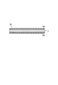
- FIG. 2 is a schematic diagram showing an example of a capacitive sensor using the capacitive sensor sheet shown in FIG.
- a capacitive sensor 101 shown in FIG. 2 includes the capacitive sensor sheet 1 shown in FIG. 1, external wirings 102 and 103, and measuring means 104.
- Each of the front side connection portions 01A1 to 16A1 of the capacitance type sensor sheet 1 is connected to the measuring means 104 via the external wiring 103 in which a plurality of (16) wires are bundled, and the back side connection portion 01B1.
- Each of .about.16B1 is connected to the measuring means 104 via an external wiring 102 in which a plurality (16) of wirings are bundled.
- the external wiring may be connected to only one end of the front side electrode layer and the back side electrode layer as shown in FIG. 2, but may be connected to both ends depending on circumstances.
- the measurement unit 104 includes a power supply circuit, an arithmetic circuit, a capacitance, a measurement circuit, a pixel switching circuit, a display device, and the like as necessary. Specific examples thereof include an LCR meter and the like.
- a capacitive sensor including such a capacitive sensor sheet is also one aspect of the present invention.
- the appearance of the capacitive sensor sheet 1 such as the average thickness, width, and length can be appropriately changed depending on the use of the capacitive sensor sheet 1 used.
- the dielectric layer has a sheet shape and is made of an elastomer composition containing urethane rubber.
- the planar view shape of the dielectric layer is not particularly limited, and may be a rectangular shape as shown in FIG. 1A, or may be another shape such as a circular shape.
- the elastomer composition contains at least urethane rubber. Since the capacitive sensor sheet of the present invention includes a dielectric layer made of an elastomer composition containing urethane rubber, it is particularly excellent in that it has excellent adhesion to an electrode layer made of a conductive composition containing carbon nanotubes.
- the conductive composition may be composed only of carbon nanotubes.
- the dielectric layer is made of an elastomer composition containing urethane rubber, and urethane rubber has a small permanent strain (or permanent elongation), so even if it is repeatedly used (for example, 1000 times of expansion and contraction is repeated)
- the initial capacitance (capacitance at no load) does not change, and excellent measurement accuracy can be maintained over a long period of time.
- the urethane rubber is not particularly limited, and is an olefin urethane rubber having an olefin polyol as a polyol component, an ester urethane rubber having an ester polyol as a polyol component, an ether urethane rubber having an ether polyol as a polyol component, and a carbonate.
- Examples thereof include carbonate-based urethane rubber using a polyol as a polyol component and castor oil-based urethane rubber using a castor oil-based polyol as a polyol component. These may be used alone or in combination of two or more.
- the urethane rubber may be a combination of two or more polyol components.
- olefin-based urethane rubber is preferable from the viewpoint of high volume resistivity
- ester-based urethane rubber is preferable from the viewpoint of high elongation and high relative dielectric constant.
- various urethane rubbers can be mixed in consideration of volume resistivity, elongation rate and dielectric constant to be applied to the dielectric layer.
- Examples of the olefin-based polyol include Epol (made by Idemitsu Kosan Co., Ltd.). Moreover, as said ester-type polyol, polylite 8651 (made by DIC Corporation) etc. are mentioned, for example.
- Examples of the ether polyol include polyoxytetramethylene glycol, PTG-2000SN (Hodogaya Chemical Co., Ltd.), polypropylene glycol, and Preminol S3003 (Asahi Glass Co., Ltd.).
- the elastomer composition may contain additives such as a plasticizer, a chain extender, a crosslinking agent, a catalyst, a vulcanization accelerator, an antioxidant, an antioxidant, and a colorant in addition to the urethane rubber. .
- the elastomer composition may further contain a dielectric filler such as barium titanate.
- a dielectric filler such as barium titanate.
- its content in the elastomer composition is usually more than 0% by volume and about 25% by volume or less.
- the content of the dielectric filler exceeds 25% by volume, the hardness of the dielectric layer may increase or permanent set may increase.
- the liquid viscosity before curing becomes high, so that it may be difficult to form a highly accurate thin film.
- the average thickness of the dielectric layer is preferably 10 to 1000 ⁇ m from the viewpoint of improving the detection sensitivity by increasing the capacitance C and improving the followability to the measurement object. More preferably, the thickness is 30 to 200 ⁇ m.
- the relative dielectric constant of the dielectric layer at room temperature is preferably 2 or more, and more preferably 5 or more.
- the capacitance C becomes small, and there is a possibility that sufficient sensitivity cannot be obtained when used as a sensor.
- the Young's modulus of the dielectric layer is preferably 0.1 to 1 MPa.
- the Young's modulus is less than 0.1 MPa, the dielectric layer is too soft, high quality processing is difficult, and sufficient measurement accuracy may not be obtained.
- the Young's modulus exceeds 1 MPa, the dielectric layer is too hard, and when the deformation load of the measurement object is small, the deformation operation of the measurement object is hindered, and the measurement result may not match the measurement purpose. .
- the dielectric layer has a hardness of 0 to 30 ° using a type A durometer according to JIS K 6253 (JIS A hardness), or a type C durometer according to JIS K 7321 is used.
- the hardness (JIS C hardness) is preferably 10 to 55 °. If the hardness using the type C durometer is less than 10 °, the dielectric layer is too soft, making high quality processing difficult, and sufficient measurement accuracy may not be ensured. On the other hand, using the type C durometer If the hardness exceeds 55 °, the dielectric layer is too hard, so that the deformation operation of the measurement object is hindered when the deformation load of the measurement object is small, and the measurement result may not match the measurement purpose. is there.
- Both the front-side electrode layer and the back-side electrode layer are made of a conductive composition containing carbon nanotubes.
- the front side electrode layer and the back side electrode layer are also simply referred to as an electrode layer.
- the said front side electrode layer and the back side electrode layer are normally formed using the same material, it does not necessarily need to use the same material.
- the carbon nanotube may be a single-walled carbon nanotube (SWNT) or a multi-walled carbon nanotube (MWNT). Of these, single-walled carbon nanotubes having a smaller diameter and a larger aspect ratio are preferred.
- SWNT single-walled carbon nanotube
- MWNT multi-walled carbon nanotube
- the average length of the carbon nanotube is preferably 1 ⁇ m or more, more preferably 10 ⁇ m or more, still more preferably 100 ⁇ m or more, particularly preferably 300 ⁇ m or more, and most preferably 600 ⁇ m or more.
- the upper limit of the average length of the carbon nanotube is not particularly limited, but is about 1000 ⁇ m.
- the aspect ratio of the carbon nanotube is preferably 100 or more, more preferably 1000 or more, still more preferably 10,000 or more, and particularly preferably 30000 or more.
- the dielectric layer when the dielectric layer is repeatedly stretched, it has excellent long-term reliability because there is little variation in electrical resistance.
- the reason for this is considered to be that, in the case of a long carbon nanotube, the carbon nanotube itself easily expands and contracts, and as a result, the conductive path is less likely to be cut when the electrode layer extends following the dielectric layer.
- conductivity is manifested when the carbon nanotubes come into contact with each other (form an electrical contact).
- conductivity is ensured with a smaller number of electrical contacts than when short carbon nanotubes are used.
- the shape (average length and aspect ratio) of the carbon nanotube used depends on the purpose of use of the capacitive sensor, conductivity and durability required for the electrode layer, What is necessary is just to select suitably, comprehensively judging the process and expense for forming an electrode layer.
- the present invention it is advantageous from the following points to use long carbon nanotubes (carbon nanotubes having a long length and a large aspect ratio).
- a method for improving the conductivity of the electrode layer made of carbon nanotubes generally, a method of coating or mixing the electrode layer with a low molecular material such as a charge transfer material or an ionic liquid as a dopant can be considered.
- a dopant when used in the electrode layer included in the capacitive sensor sheet of the present invention, there is a concern that the dopant may migrate into the dielectric layer.
- the dielectric layer may have a reduced insulation property (decrease in volume resistivity) and a decrease in durability during repeated use, and as a result, measurement accuracy may be reduced.
- the above-mentioned long carbon nanotube is used as the carbon nanotube, sufficient conductivity can be imparted to the electrode layer without using a dopant.
- the carbon nanotubes preferably have a purity of 99% by weight or more.
- Carbon nanotubes may contain catalytic metals, non-nanotube carbon materials (amorphous carbon, graphite, etc.), dispersants and the like in the production process.
- an electrode layer is formed using carbon nanotubes containing a large amount of components (impurities) other than carbon nanotubes, the conductivity and elongation of the electrode layer may decrease, and the elastic modulus of the electrode layer This is because the sensor sheet is hardened and the stretchability of the sensor sheet may be lowered.
- the conductive composition may contain a binder component as a connecting material for the carbon nanotube.
- a binder component By containing the binder component, the adhesion to the dielectric layer and the strength of the electrode layer itself can be improved. Furthermore, by containing the binder component, it is possible to suppress the scattering of the carbon nanotubes when forming the electrode layer by the method described later, and thus it is possible to improve the safety when forming the electrode layer.
- the binder component urethane rubber is preferable, and urethane rubber of the same type as the urethane rubber constituting the dielectric layer is particularly preferable. This is because the adhesion between the dielectric layer and the electrode layer can be remarkably improved.
- the binder component may be a binder component other than urethane rubber.
- a binder component from a polymer having a solubility parameter (SP value) close to that of urethane rubber (for example, a polymer whose difference from the SP value of urethane rubber is ⁇ 1).
- SP value solubility parameter
- a binder component is preferred.
- Specific examples of such a binder component include, for example, polyisoprene, butyl rubber, ethylene propylene rubber, polyethylene, chlorosulfonated polyethylene, natural rubber, isoprene rubber, butadiene rubber, styrene-butadiene rubber, polystyrene, chloroprene rubber, and nitrile rubber.
- polymethyl methacrylate polyvinyl acetate, polyvinyl chloride, acrylic rubber, styrene-ethylene-butylene-styrene block copolymer (SEBS), and the like.
- binder component raw rubber (in a state where natural rubber and synthetic rubber are not vulcanized) can also be used. By using a material having relatively weak elasticity such as raw rubber, the followability of the electrode layer to the deformation of the dielectric layer can be enhanced.
- the conductive composition may contain various additives in addition to the carbon nanotube and the binder component.
- the additive include a dispersant for enhancing the dispersibility of carbon nanotubes, a crosslinking agent for a binder component, a vulcanization accelerator, a vulcanization aid, an anti-aging agent, a plasticizer, a softening agent, and a colorant.
- Etc a dispersant for enhancing the dispersibility of carbon nanotubes
- a crosslinking agent for a binder component a vulcanization accelerator, a vulcanization aid, an anti-aging agent, a plasticizer, a softening agent, and a colorant.
- Etc when the conductive composition contains a plasticizer and the elastomer composition also contains a plasticizer, it is preferable that the plasticizer concentration is the same in both compositions. This is because it is possible to prevent the plasticizer from being transferred between the dielectric layer and the electrode layer, thereby suppressing the occurrence of warpage and
- the electrode layer can be formed substantially only from carbon nanotubes.
- the dielectric layer is made of an elastomer composition containing urethane rubber, sufficient adhesion between the dielectric layer and the electrode layer made of only carbon nanotubes is ensured. Because it can be done.
- the content of carbon nanotubes in the electrode layer is not particularly limited as long as it is a concentration at which conductivity is exhibited.
- the binder component When the binder component is contained, it varies depending on the type of the binder component, but the total solid component of the electrode layer is different. It is preferably 0.1 to 100% by weight.
- By increasing the content of carbon nanotubes it is possible to suppress a decrease in conductivity (increase in electric resistance) of the electrode layer when it is repeatedly deformed, and to have excellent durability.
- the amount of the carbon nanotube is small and the amount of the binder component is large, the elasticity of the electrode layer is increased, which becomes a buffer layer against deformation and displacement of the measurement object, and there is a possibility that the measurement accuracy is lowered.
- the average thickness of the electrode layer (the average thickness of each of the front-side electrode layer and the back-side electrode layer) is preferably 0.1 to 10 ⁇ m. This is because when the average thickness of the electrode layer is in the above range, the electrode layer can exhibit excellent followability to the deformation of the dielectric layer. On the other hand, when the average thickness is less than 0.1 ⁇ m, the electrical conductivity is insufficient and the measurement accuracy may be lowered. On the other hand, when the average thickness exceeds 10 ⁇ m, the capacitive sensor sheet becomes hard due to the reinforcing effect of the carbon nanotubes, the followability to the measurement object is lowered, and deformation such as expansion and contraction may be hindered.
- the “average thickness of the electrode layer” is measured using a laser microscope (for example, VK-9510 manufactured by Keyence Corporation). Specifically, after scanning the thickness direction of the electrode layer laminated on the surface of the dielectric layer in steps of 0.01 ⁇ m and measuring its 3D shape, the region where the electrode layer is laminated on the surface of the dielectric layer and In the non-stacked region, the average height of each rectangular region of length 200 ⁇ width 200 ⁇ m is measured, and the step of the average height is defined as the average thickness of the electrode layer.
- a laser microscope for example, VK-9510 manufactured by Keyence Corporation
- the transparency (visible light transmittance) of the front side electrode layer and the back side electrode layer is not particularly limited, and may be transparent or opaque.
- the dielectric layer is made of an elastomer composition containing urethane rubber, and can be easily formed into a transparent dielectric layer. Therefore, in the said capacitive sensor sheet, it can be set as a transparent capacitive sensor sheet as a whole by improving the transparency of the said front side electrode layer and the said back side electrode layer.
- the carbon nanotubes require a pretreatment such as a high degree of dispersion treatment or purification treatment, so the electrode layer formation process is complicated. It becomes disadvantageous economically.
- the transparency of the electrode layer does not affect the performance as a capacitive sensor sheet. Therefore, when transparency is required as the capacitance type sensor sheet, a transparent electrode layer (for example, visible light (550 nm light) transmittance of 85% or more) may be formed, and transparency is not required. For this, an opaque electrode layer may be formed. An opaque electrode layer can be manufactured more easily and inexpensively.
- ⁇ Detection unit C0101 to C1616 in FIG. 1>
- the detection portions C0101 to C1616 are arranged at portions (overlapping portions) where the front-side electrode layers 01A to 16A and the back-side electrode layers 01B to 16B intersect in the thickness direction of the dielectric layer. ing.
- the detection units C0101 to C1616 are arranged at substantially equal intervals over substantially the entire surface of the capacitive sensor sheet 1.
- the detection units C0101 to C1616 include a part of the front side electrode layers 01A to 16A, a part of the back side electrode layers 01B to 16B, and a part of the dielectric layer 2, respectively.
- the change amount ⁇ C of the capacitance is detected from the capacitance C before placing the measurement object and the capacitance C after placing the measurement object.
- the amount of expansion / contraction deformation strain and the distribution of expansion / contraction deformation strain can be obtained.
- the capacitive sensor sheet of the present invention has a high elongation rate, and can be repeatedly stretched by 30% or more in one axial direction, and can follow the deformation and operation of a flexible measurement object. And, it is excellent in durability against expansion and contraction deformation and repetitive deformation.
- the shape of the measurement object can be traced, or the movement of the measurement object can be directly detected.
- FIG. 3 is a plan view schematically showing another example of the capacitive sensor sheet of the present invention.
- a capacitive sensor sheet 1 'shown in FIG. 3 includes a sheet-like dielectric layer 2', strip-shaped front electrode layers 01D to 16D laminated on the surface of the dielectric layer 2 ', and a back surface of the dielectric layer 2'.
- the portions where the front-side electrode layer and the back-side electrode layer intersect in the front-back direction (thickness direction of the dielectric layer) are detection units F0101 to F1616. It should be noted that in the detection unit code “FXXX”, the upper two digits “XX” correspond to the front electrode layers 01D to 16D, and the lower two digits “ ⁇ ” indicate the back electrode layers 01E to 01D. Corresponding to 16E.
- the front electrode layers 01D to 16D each have a strip shape, and a total of 16 layers are laminated on the surface of the dielectric layer 2 ′.
- the front side electrode layers 01D to 16D each extend in the X direction (left and right direction in FIG. 3).
- the front-side electrode layers 01D to 16D are respectively arranged so as to be substantially parallel to each other at a predetermined interval in the Y direction (vertical direction in FIG. 3).
- Linear front-side wirings 01d to 16d extending in the Y direction are connected to the left ends of the front-side electrode layers 01D to 16D, respectively.
- the other ends of the front-side wirings 01d to 16d extend to the outer edge portion of the dielectric layer 2 '.
- the back-side electrode layers 01E to 16E each have a strip shape, and a total of 16 layers are laminated on the back surface of the dielectric layer 2 ′.
- the back-side electrode layers 01E to 16E are arranged so as to intersect the front-side electrode layers 01D to 16D at substantially right angles when viewed from the front and back directions. That is, the back side electrode layers 01E to 16E each extend in the Y direction. Further, the back side electrode layers 01E to 16E are arranged so as to be substantially parallel to each other at a predetermined interval in the X direction. Linear backside wires 01e to 16e extending in the X direction are connected to one ends (upper ends) of the backside electrode layers 01E to 16E, respectively. The other ends of the back-side wirings 01e to 16e extend to the outer edge portion of the dielectric layer 2 '.
- the material constituting the front side wiring and the back side wiring is not particularly limited, and materials conventionally used for electrical wiring can be used.
- Each wiring (front side wiring and back side wiring) can be stretched and deformed by having the same configuration as the layer, which is preferable because it does not hinder the deformation of the sensor sheet by the measurement object. More specifically, using the same conductive composition as the conductive composition on which the electrode layer is formed, the front side wiring and the back side wiring are formed so that the line width is narrow and the thickness is thick.
- the front side wiring and the back side wiring are formed so that the line width is narrow and the thickness is thick.
- the capacitive sensor sheet 1 ′ can be connected to external wiring via this connector.
- the capacitive sensor sheet 1 ′ having such a configuration also measures each of the front side electrode layer and the back side electrode layer via external wiring, similarly to the capacitive type sensor sheet 1 shown in FIGS. By connecting to the means, a capacitive sensor is obtained.
- the capacitance type sensor sheet of the present invention may have a configuration as shown in FIG.
- FIG. 4 is a cross-sectional view schematically showing another example of the capacitive sensor sheet of the present invention.
- the capacitive sensor sheet 44 shown in FIG. 4 is the same as the capacitive sensor sheet 1 shown in FIG. 1 except that the front side overcoat layer 44A is formed on the outermost layer on the front side, and the back side overcoat layer is on the outermost layer on the back side. 44B is formed.
- the electrode layer can be protected from an external impact. Moreover, in the said capacitive sensor sheet
- the overcoat layer is formed, the purpose thereof is not limited to the protection of the electrode layer. For example, by forming a colored overcoat layer, the electrode layer can be made invisible from the outside. By coloring only the portion, it is possible to impart design properties to the capacitive sensor sheet.
- the surface of the overcoat layer may be printed.
- the measurement object can be attached to the capacitive sensor sheet, and, for example, the surface of the overcoat layer has a coefficient of friction. And a low ⁇ surface layer with a low thickness.
- the capacitive sensor sheet of the present invention is used as an input interface for a flexible and stretchable touch panel.
- An example is given.
- a pseudo button, a keyboard, a product logo, or the like at the input position is printed on the surface of the overcoat layer.
- printing may be performed by inkjet printing, screen printing, gravure printing, or the like using, for example, water-based ink, solvent-based ink, UV curable ink, or the like. More specifically, for example, in the case of a solvent-based ink, a conventionally known solvent-based ink mainly composed of a solvent, a pigment, a vehicle, and an auxiliary agent blended as necessary may be used.
- examples of the solvent include glycol ether solvents such as diethylene glycol diethyl ether, tetraethylene glycol dimethyl ether and tetraethylene glycol monobutyl ether, lactone solvents such as ⁇ -butyrolactone, low-boiling aromatic naphtha, and propylene glycol monomethyl ether.
- examples of the solvent include glycol ether solvents such as diethylene glycol diethyl ether, tetraethylene glycol dimethyl ether and tetraethylene glycol monobutyl ether, lactone solvents such as ⁇ -butyrolactone, low-boiling aromatic naphtha, and propylene glycol monomethyl ether.
- examples of the pigment include carbon black (black), copper phthalocyanine (cyan), dimethylquinacridone (magenta), pigment yellow (yellow), titanium oxide, aluminum oxide, zirconium oxide, and nickel compounds.
- Various pigments are known and of course not limited to the above.
- the material of the overcoat layer is not particularly limited and may be appropriately selected depending on the purpose of formation.
- a colorant pigment
- a composition containing a dye can be preferably used.
- the overcoat layer may be formed only on either the front side or the back side.
- the present invention can be carried out in various modifications and improvements in addition to the above embodiment.
- the number of front side electrode layers 01A to 16A and the number of rear side electrode layers 01B to 16B is set to 16, but this number is not particularly limited.
- the crossing angle of the front electrode layers 01A to 16A and the back electrode layers 01B to 16B in the above embodiment is not particularly limited.
- the capacitance type sensor sheet is, for example, (1) a step of forming a dielectric layer made of an elastomer composition (hereinafter also referred to as “step (1)”), and (2) application of a composition containing carbon nanotubes and a dispersion medium, Step of forming an electrode layer on the back surface (hereinafter also referred to as “step (2)”) It can manufacture by going through.
- step (1) a step of forming a dielectric layer made of an elastomer composition
- step (2) Step of a composition containing carbon nanotubes and a dispersion medium
- a dielectric layer is formed using the elastomer composition.
- urethane rubber or its raw materials: polyol component and isocyanate component
- dielectric filler if necessary, dielectric filler, plasticizer, chain extender, crosslinking agent, vulcanization accelerator, catalyst, antioxidant, An elastomer composition containing additives such as an anti-aging agent and a colorant is prepared.
- the method for preparing the elastomer composition and the method for forming the dielectric layer are not particularly limited, and conventionally known methods can be used. Specifically, for example, a polyol component, a plasticizer, and an antioxidant are measured.
- the mixture is stirred and mixed for a certain time under heating and reduced pressure to prepare a mixed solution.
- the catalyst is added and stirred with an agitator or the like.
- a predetermined amount of an isocyanate component is added, and after stirring with an agitator or the like, the mixed solution is immediately poured into a molding apparatus shown in FIG. A roll-wrapped sheet having a predetermined thickness is obtained.
- the dielectric layer can be produced by further performing a crosslinking reaction (post-crosslinking) for a certain period of time in a furnace.
- FIG. 5 is a schematic diagram for explaining an example of a molding apparatus used for producing a dielectric layer.
- the raw material composition 33 is poured into a gap between a protective film 31 made of polyethylene terephthalate (PET) that is continuously fed from a pair of rolls 32 and 32 ′ that are spaced apart from each other.
- PET polyethylene terephthalate
- the curing reaction crosslinking reaction
- the curing reaction is allowed to proceed while holding the raw material composition 33 in the gap, and is introduced into the heating device 34, and the raw material composition 33 is thermally cured while being held between the pair of PET films 31.
- the sheet-like dielectric layer 35 is formed.
- the dielectric layer may be formed using a general-purpose film forming apparatus or film forming method such as various coating apparatuses, bar coats, doctor blades and the like.
- Electrodes front-side electrode layer and back-side electrode layer
- electrode layers are formed on the front and back surfaces of the dielectric layer by applying a composition containing carbon nanotubes and a dispersion medium.
- carbon nanotubes are added to a dispersion medium such as toluene.
- a binder component or a raw material for the binder component
- a dispersant or other various additives may be added.
- a coating liquid is prepared by dispersing (or dissolving) each component including carbon nanotubes in a dispersion medium using a wet disperser.
- an existing disperser such as an ultrasonic disperser, a jet mill, or a bead mill may be used for dispersion.
- the dispersion medium is not limited to toluene, and other examples include methyl isobutyl ketone (MIBK), alcohols, and water. These dispersion media may be used independently and may be used together 2 or more types.
- the concentration of the carbon nanotube is preferably 0.01 to 10% by weight. If it is less than 0.01% by weight, the concentration of the carbon nanotubes may be too thin to be repeatedly applied. On the other hand, if it exceeds 10% by weight, the viscosity of the coating solution becomes too high, and the carbon nanotubes are re-aggregated. In some cases, it is difficult to form a uniform electrode layer.
- a coating solution prepared in a predetermined shape (band shape) is applied to a predetermined position on the surface of the dielectric layer and dried.
- the electrode layers are, for example, about 1 mm to 20 mm in width and about 50 mm to 500 mm in length, and are formed so as to be substantially parallel to each other with an interval of about 1 mm to 5 mm.
- the coating liquid may be applied after masking a position where the electrode layer on the surface of the dielectric layer is not formed.
- the drying conditions for the coating solution are not particularly limited, and may be appropriately selected according to the type of the dispersion medium.
- the method of applying the coating liquid of the conductive composition is not limited to the method using an air brush, and other methods such as a screen printing method and an ink jet printing method can also be employed.
- the surface of the dielectric layer may be pretreated in order to improve the adhesion between them.
- the elastomer composition and the conductive composition according to the present invention have extremely excellent adhesion, sufficient adhesion between the dielectric layer and the electrode layer can be obtained without any pretreatment. Can be secured.
- the material for overcoat layers should be apply
- various coating apparatuses general-purpose film forming apparatuses such as a bar coat, a doctor blade, and a film forming method can be used.
- a cross-linked or semi-cross-linked sheet can be separately prepared, and this sheet can be laminated to a dielectric layer on which an electrode layer is formed to form an overcoat layer.
- semi-crosslinking complete cross-linking may be performed after bonding.
- the capacitive sensor sheet of the present invention can be manufactured through such steps.
- the capacitive sensor sheet including the overcoat layer can be manufactured through the following steps, for example. That is, one overcoat layer is first prepared, and then an electrode layer (front side electrode layer or back side electrode layer) is formed on the overcoat layer by the same method as in the above step (2). Thereafter, a dielectric layer made of an elastomer composition containing urethane rubber, which has been separately prepared, is pasted on the electrode layer (laminate). Subsequently, an electrode layer (back side electrode layer or front side electrode layer) is formed on the dielectric layer by the same method as in the above step (2), and finally the other overcoat layer is formed.
- the dielectric layer thus prepared was measured for elongation at break (%), volume resistivity ( ⁇ cm), and relative dielectric constant.
- the elongation at break (%) was 218%, the volume resistivity was 1 ⁇ 10 14 ⁇ cm or more, the ratio The dielectric constant was 3.1.
- the elongation at break was measured according to JIS K 6251.
- the volume resistivity was measured in accordance with JIS K 6911 using Hiresta UP MCP-HT450 type (manufactured by Mitsubishi Chemical Analytech Co.) as a measuring instrument and URS probe MCP-HTP14 as a probe.
- the relative dielectric constant was measured in accordance with JIS K 6911 using an LCR HiTester 3522-50 (manufactured by Hioki Electric Co., Ltd.) as a measuring instrument.
- isophorone diisocyanate (Desmodur I, manufactured by Sumika Bayer Urethane Co., Ltd.) was added, and the mixture was stirred for 3 minutes with a rotation and revolution mixer and defoamed for 1.5 minutes. Then, it is injected into the molding apparatus 30 shown in FIG. 5, and is cross-linked and cured at a furnace temperature of 110 ° C. and a furnace time of 30 minutes while being transported in a sandwich form with a protective film, and a roll having a predetermined thickness with a protective film. A roll sheet was obtained.
- isophorone diisocyanate (Desmodur I, manufactured by Sumika Bayer Urethane Co., Ltd.) was added, stirred for 3 minutes with a rotating / revolving mixer, defoamed for 1.5 minutes, and then added to the molding apparatus 30 shown in FIG. It was injected and cross-linked and cured under the conditions of a furnace temperature of 110 ° C. and a furnace time of 30 minutes while being transported in a sandwich form with a protective film to obtain a roll-wrapped sheet having a predetermined thickness with a protective film. Thereafter, a crosslinking reaction was carried out for 720 minutes in a furnace adjusted to 80 ° C.
- a dielectric layer having a layer thickness of 50 ⁇ m made of an elastomer composition containing an ether-based urethane rubber Regarding the produced dielectric layer, the elongation at break (%), volume resistivity ( ⁇ cm) and relative dielectric constant were measured in the same manner as in Production Example 1. The elongation at break (%) was 280%, and the volume resistivity was 2 .58 ⁇ 10 11 ⁇ cm and the relative dielectric constant was 5.2.
- EPDM dielectric layer 1.1 parts by mass of Park Mill D (manufactured by Nippon Oil & Fats Co., Ltd.) as a peroxide cross-linking agent was added to 100 parts by mass of EPDM (Esplen 600F, manufactured by Sumitomo Chemical Co., Ltd.) to obtain a roll-kneaded raw rubber. This raw rubber was press-molded at 160 ° C. for 20 minutes to be crosslinked to produce an EPDM dielectric layer having a layer thickness of 50 ⁇ m.
- Preparation Example 1 As carbon nanotubes, super-growth CNT (hereinafter also referred to as “SGCNT”) (median fiber diameter is about 3 nm, growth length is 500 ⁇ m to 700 ⁇ m, aspect ratio is about 100,000, carbon purity is 99.9%, industrial technology 30 mg of toluene (provided by Research Institute) was added to 280 ml of toluene, and wet dispersion treatment was performed using a jet mill (NanoJet Pal JN10-SP003, manufactured by Joko) to obtain an electrode layer forming coating solution (A-1). .
- the growth length of the carbon nanotube refers to the height of the forest grown on the growth substrate when the carbon nanotube is produced.
- Preparation Example 2 A coating solution for electrode layer formation (as in Preparation Example 1) except that VGCF-X (length: 3 ⁇ m, aspect ratio: about 200, carbon purity: 95% or higher, registered trademark, manufactured by Showa Denko KK) was used as the carbon nanotube. A-2) was obtained.
- the other line (upper line) extending from the point representing the electrical resistance value at the time represents the change in electrical resistance when returning from the first elongation rate of 100% to the elongation rate of 0% (on the return path).
- the number of repetitions is one for the forward and return routes.
- two lines whose resistance value at the time of 100% elongation extends from the second point from the bottom represents the change in the electric resistance of the second repetition number, and among these, the lower line is the outward path of the second repetition number.
- the change in the electrical resistance at the time of the return is represented, and the upper line represents the change in the electrical resistance during the second return.
- changes in electrical resistance after the third repetition are also shown in FIGS.
- the electrode layer forming coating solution (A-1) was applied in a strip shape with an air brush and dried to form a front electrode layer.
- the front electrode layer is a strip-shaped electrode layer arranged in parallel with each other, and five layers having an average thickness of about 1 ⁇ m, a width of 10 mm, and a length of 100 mm were formed at intervals of 5 mm.
- the electrode layer forming coating solution (A-1) was applied to the back surface of the dielectric layer so as to be orthogonal to the front electrode layer, and formed in the same manner. Thereafter, both ends of each belt-like electrode layer were reinforced with a 0.1 mm thick copper foil, and lead wires of external wirings (front side wiring and back side wiring) were screwed and connected to form a sensor sheet 1.
- a sensor sheet 2 was produced in the same manner as in Example 1 except that the dielectric layer made of EPDM produced in Production Example 4 was used as the dielectric layer.
- Each of the sensor sheets 1 and 2 was restrained on two sides with a resin frame 23 as shown in FIG. 8 and uniaxial stretching was repeated until the frame was stretched to 100% in one axial direction, and the change in capacitance was measured.
- 01A 'to 05A' are front side electrode layers
- 01B 'to 05B' are back side electrode layers
- 01A'1 to 05A'1 are front side connection parts
- 01B'1 to 05B'1 are back side connection parts
- C′0101 to C′0505 are detectors
- 22 is an elastomeric dielectric layer.
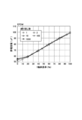
- the measurement results are shown in Table 1, and the average capacitance of the 25 detection units was plotted against the uniaxial extension rate.
- the sensor sheet 1 is shown in FIG. 9, and the sensor sheet 2 is shown in FIG.
- An LCR meter manufactured by Hioki Electric Co., Ltd., LCR HiTester 3522-50 was used for capacitance measurement.
- the sensor sheet 1 (Example 1) increased in capacitance almost linearly from the steady state to the 100% extended state
- the sensor sheet 2 In Comparative Example 1
- the capacitance in the steady state increases as the number of repetitions increases.
- the capacitance type sensor sheet having a dielectric layer made of urethane rubber is excellent in measurement accuracy during repeated measurement.
- the sensor sheet 2 having a dielectric layer made of EPDM it was clarified that the reason why the capacitance in the steady state gradually increased was that the permanent deformation (permanent elongation) of EPDM was large. .
- FIG. 11 is a three-dimensional graph showing the stretch deformation strain distribution detected by the sensor sheet 1.
- Electrode layer-forming coating solution (A-1) was applied to one side of the dielectric layer produced in Production Examples 1 to 3 and 5 with an airbrush and dried at 80 ° C. for 1 hour to form an electrode layer having a width of 10 mm.
- An evaluation sample was prepared. Then, for each evaluation sample, a masking tape (manufactured by Nitto Denko Corporation, masking tape No. 720) was attached to the electrode layer (SGCNT film) and then peeled off, and the state of the electrode layer before and after that was visually observed.
- a masking tape manufactured by Nitto Denko Corporation, masking tape No. 720
- the capacitive sensor sheet of the present invention can be suitably used as a capacitive sensor sheet for measuring at least one of the amount of stretching deformation strain and the stretching deformation strain distribution.
- the capacitive sensor using the capacitive sensor sheet of the present invention is used as, for example, a sensor for tracing the shape of a flexible object or a sensor for measuring the movement of a measurement object such as a person. be able to. More specifically, for example, it is possible to measure (detect) the deformation of the shoe sole inner by the sole, the deformation of the seat cushion by the heel, and the like.
- the said capacitive type sensor can be used also as an input interface for touch panels, for example.
- the capacitance type sensor of the present invention can also be used for measurement at a light shielding part that cannot be measured by an optical motion capture which is an existing sensor.
Landscapes
- Physics & Mathematics (AREA)
- General Physics & Mathematics (AREA)
- Engineering & Computer Science (AREA)
- Power Engineering (AREA)
- Measurement Of Length, Angles, Or The Like Using Electric Or Magnetic Means (AREA)
Abstract
La présente invention concerne une feuille de capteur capacitif pour utilisation dans la mesure de la quantité de l'expansion/déformation/allongement et/ou la distribution d'expansion/déformation/allongement. Cette feuille de capteur capacitif, qui est destinée à une utilisation dans la mesure de la quantité d'expansion/déformation/allongement et/ou la distribution d'expansion/déformation/allongement, comprend une couche diélectrique, des couches d'électrode côté avant formées sur la surface avant de la couche diélectrique, et des couches d'électrode côté arrière formées sur la surface arrière de la couche diélectrique, la couche diélectrique étant constituée d'une composition d'élastomère contenant un caoutchouc d'uréthane et les couches d'électrode côté avant et les couches d'électrode côté arrière étant constituées d'une composition électroconductrice contenant des nanotubes de carbone.
Priority Applications (2)
| Application Number | Priority Date | Filing Date | Title |
|---|---|---|---|
| JP2015508765A JPWO2014157627A1 (ja) | 2013-03-29 | 2014-03-28 | 静電容量型センサシート及び静電容量型センサ |
| US14/868,258 US10365171B2 (en) | 2013-03-29 | 2015-09-28 | Capacitive sensor sheet and capacitive sensor for measuring elastic deformation |
Applications Claiming Priority (2)
| Application Number | Priority Date | Filing Date | Title |
|---|---|---|---|
| JP2013-074030 | 2013-03-29 | ||
| JP2013074030 | 2013-03-29 |
Related Child Applications (1)
| Application Number | Title | Priority Date | Filing Date |
|---|---|---|---|
| US14/868,258 Continuation US10365171B2 (en) | 2013-03-29 | 2015-09-28 | Capacitive sensor sheet and capacitive sensor for measuring elastic deformation |
Publications (1)
| Publication Number | Publication Date |
|---|---|
| WO2014157627A1 true WO2014157627A1 (fr) | 2014-10-02 |
Family
ID=51624583
Family Applications (1)
| Application Number | Title | Priority Date | Filing Date |
|---|---|---|---|
| PCT/JP2014/059143 WO2014157627A1 (fr) | 2013-03-29 | 2014-03-28 | Feuille de capteur capacitif et capteurs capacitifs |
Country Status (3)
| Country | Link |
|---|---|
| US (1) | US10365171B2 (fr) |
| JP (2) | JPWO2014157627A1 (fr) |
| WO (1) | WO2014157627A1 (fr) |
Cited By (3)
| Publication number | Priority date | Publication date | Assignee | Title |
|---|---|---|---|---|
| WO2017159136A1 (fr) * | 2016-03-17 | 2017-09-21 | アルプス電気株式会社 | Dispositif d'entrée et son procédé de production |
| CN108195336A (zh) * | 2017-12-26 | 2018-06-22 | 深圳市宇恒互动科技开发有限公司 | 物体三维外形的感测方法、装置及系统 |
| CN111829432A (zh) * | 2020-07-27 | 2020-10-27 | 上海大学 | 一种具有双层传感结构可模块化使用的软体曲率传感器 |
Families Citing this family (11)
| Publication number | Priority date | Publication date | Assignee | Title |
|---|---|---|---|---|
| WO2015053638A1 (fr) | 2013-10-10 | 2015-04-16 | Stretchsense Limited | Procédé de fabrication de stratifiés composés d'un matériau élastique convenant pour permettre la détection d'un élastomère diélectrique |
| KR101731173B1 (ko) * | 2015-09-02 | 2017-04-28 | 한국과학기술원 | 다공성 탄성중합체 유전층을 구비하는 정전용량형 압력센서 |
| CN107290082B (zh) * | 2016-04-11 | 2019-12-20 | 刘垚 | 一种电容式触觉传感器 |
| TWI623732B (zh) * | 2016-12-29 | 2018-05-11 | 台灣艾華電子工業股份有限公司 | 分層異向位移型拉伸感測器 |
| CN108303018B (zh) * | 2017-01-13 | 2019-11-19 | 台湾艾华电子工业股份有限公司 | 分层异向位移型拉伸传感器 |
| JP6781648B2 (ja) * | 2017-03-09 | 2020-11-04 | 正毅 千葉 | 誘電エラストマーセンサシステムおよび誘電エラストマーセンサ要素 |
| WO2019166635A1 (fr) * | 2018-03-01 | 2019-09-06 | Universität Basel Vizerektorat Forschung | Transducteur élastomère diélectrique et procédé de fabrication correspondant |
| CN111936370B (zh) * | 2018-09-26 | 2022-08-09 | 住友理工株式会社 | 电容传感器、其制造方法、以及电容传感器用网眼状柔软电极 |
| CN112771358B (zh) * | 2018-10-18 | 2023-09-26 | 松下知识产权经营株式会社 | 压敏元件以及电子设备 |
| US20220268646A1 (en) * | 2019-06-26 | 2022-08-25 | Pi Bioelectronics Co., Ltd | Pressure sensing system and pressure sensing setting method |
| EP4127635A1 (fr) * | 2020-03-31 | 2023-02-08 | King Abdullah University of Science and Technology | Capteur de contrainte capacitif super-sensible avec fragmentation d'électrode |
Citations (6)
| Publication number | Priority date | Publication date | Assignee | Title |
|---|---|---|---|---|
| JP2010043881A (ja) * | 2008-08-08 | 2010-02-25 | Tokai Rubber Ind Ltd | 静電容量型面圧分布センサ |
| WO2010095581A1 (fr) * | 2009-02-18 | 2010-08-26 | 株式会社クラレ | Capteur de déformation multicouche |
| JP2011017626A (ja) * | 2009-07-09 | 2011-01-27 | Sony Corp | 力学量検知部材及び力学量検知装置 |
| JP2012032325A (ja) * | 2010-08-02 | 2012-02-16 | Sony Corp | 形状センサおよび情報入力装置 |
| WO2012105690A1 (fr) * | 2011-02-04 | 2012-08-09 | 信越ポリマー株式会社 | Feuille de détection capacitive et son procédé de fabrication |
| JP2012225727A (ja) * | 2011-04-19 | 2012-11-15 | Tokai Rubber Ind Ltd | 静電容量型センサ装置 |
Family Cites Families (21)
| Publication number | Priority date | Publication date | Assignee | Title |
|---|---|---|---|---|
| TW350026B (en) | 1995-07-28 | 1999-01-11 | Hokushin Ind | Pressure sensor |
| JP4063564B2 (ja) | 2002-03-25 | 2008-03-19 | ニッタ株式会社 | ポリウレタンエラストマー圧電素子及び感圧センサー並びに接触センサー |
| JP4277103B2 (ja) * | 2004-02-03 | 2009-06-10 | 国立大学法人信州大学 | カーボンナノファイバーを用いる高分子アクチュエータ |
| JP2008227384A (ja) * | 2007-03-15 | 2008-09-25 | Nsk Ltd | 誘電性ゴム積層体 |
| JP5496446B2 (ja) * | 2007-07-12 | 2014-05-21 | 東海ゴム工業株式会社 | 静電容量型センサ |
| WO2009102077A1 (fr) | 2008-02-11 | 2009-08-20 | The University Of Tokyo | Composition de caoutchouc à nanotube de carbone, câblage, pâte électroconductrice, circuit électronique et procédé de fabrication de la composition de caoutchouc à nanotube de carbone |
| US7958789B2 (en) | 2008-08-08 | 2011-06-14 | Tokai Rubber Industries, Ltd. | Capacitive sensor |
| JP4650538B2 (ja) * | 2008-08-08 | 2011-03-16 | 東海ゴム工業株式会社 | 静電容量型センサ |
| DE102008039757A1 (de) * | 2008-08-20 | 2010-02-25 | Fraunhofer-Gesellschaft zur Förderung der angewandten Forschung e.V. | Aktorelement sowie seine Verwendung |
| JP2010110090A (ja) * | 2008-10-29 | 2010-05-13 | Nsk Ltd | エラストマートランスデューザー |
| JP5474331B2 (ja) * | 2008-10-30 | 2014-04-16 | 東海ゴム工業株式会社 | 誘電膜、およびそれを用いたアクチュエータ、センサ、トランスデューサ |
| JP2010207985A (ja) * | 2009-03-11 | 2010-09-24 | Tokai Rubber Ind Ltd | 関節型駆動機構 |
| US8893561B2 (en) * | 2009-05-06 | 2014-11-25 | Xsensor Technology Corporation | Dielectric textured elastomer in a pressure mapping system |
| US8568027B2 (en) * | 2009-08-26 | 2013-10-29 | Ut-Battelle, Llc | Carbon nanotube temperature and pressure sensors |
| JP5290107B2 (ja) | 2009-09-24 | 2013-09-18 | 東海ゴム工業株式会社 | 張力センサ |
| JP5505717B2 (ja) | 2010-06-22 | 2014-05-28 | 信越ポリマー株式会社 | 導電パターンの製造方法 |
| JP5570353B2 (ja) * | 2010-09-03 | 2014-08-13 | バイエル マテリアルサイエンス株式会社 | 伸縮性配線を有する導電部材 |
| JP2012073150A (ja) * | 2010-09-29 | 2012-04-12 | Tokai Rubber Ind Ltd | 静電容量型センサ |
| JP2012123744A (ja) | 2010-12-10 | 2012-06-28 | Shin Etsu Polymer Co Ltd | 静電容量式入力装置およびその製造方法、静電容量式入力装置の入力方法 |
| CN103764556B (zh) * | 2011-09-02 | 2016-01-06 | 独立行政法人产业技术综合研究所 | 碳纳米管复合材料及导电材料 |
| US9767937B2 (en) * | 2012-02-16 | 2017-09-19 | David L. Carnahan | Conductive elastic composite |
-
2014
- 2014-03-28 WO PCT/JP2014/059143 patent/WO2014157627A1/fr active Application Filing
- 2014-03-28 JP JP2015508765A patent/JPWO2014157627A1/ja active Pending
-
2015
- 2015-09-28 US US14/868,258 patent/US10365171B2/en active Active
-
2020
- 2020-03-09 JP JP2020039927A patent/JP2020106545A/ja not_active Abandoned
Patent Citations (6)
| Publication number | Priority date | Publication date | Assignee | Title |
|---|---|---|---|---|
| JP2010043881A (ja) * | 2008-08-08 | 2010-02-25 | Tokai Rubber Ind Ltd | 静電容量型面圧分布センサ |
| WO2010095581A1 (fr) * | 2009-02-18 | 2010-08-26 | 株式会社クラレ | Capteur de déformation multicouche |
| JP2011017626A (ja) * | 2009-07-09 | 2011-01-27 | Sony Corp | 力学量検知部材及び力学量検知装置 |
| JP2012032325A (ja) * | 2010-08-02 | 2012-02-16 | Sony Corp | 形状センサおよび情報入力装置 |
| WO2012105690A1 (fr) * | 2011-02-04 | 2012-08-09 | 信越ポリマー株式会社 | Feuille de détection capacitive et son procédé de fabrication |
| JP2012225727A (ja) * | 2011-04-19 | 2012-11-15 | Tokai Rubber Ind Ltd | 静電容量型センサ装置 |
Cited By (4)
| Publication number | Priority date | Publication date | Assignee | Title |
|---|---|---|---|---|
| WO2017159136A1 (fr) * | 2016-03-17 | 2017-09-21 | アルプス電気株式会社 | Dispositif d'entrée et son procédé de production |
| CN108195336A (zh) * | 2017-12-26 | 2018-06-22 | 深圳市宇恒互动科技开发有限公司 | 物体三维外形的感测方法、装置及系统 |
| CN108195336B (zh) * | 2017-12-26 | 2020-10-09 | 深圳市宇恒互动科技开发有限公司 | 物体三维外形的感测方法、装置及系统 |
| CN111829432A (zh) * | 2020-07-27 | 2020-10-27 | 上海大学 | 一种具有双层传感结构可模块化使用的软体曲率传感器 |
Also Published As
| Publication number | Publication date |
|---|---|
| US20160018275A1 (en) | 2016-01-21 |
| JPWO2014157627A1 (ja) | 2017-02-16 |
| US10365171B2 (en) | 2019-07-30 |
| JP2020106545A (ja) | 2020-07-09 |
Similar Documents
| Publication | Publication Date | Title |
|---|---|---|
| WO2014157627A1 (fr) | Feuille de capteur capacitif et capteurs capacitifs | |
| WO2015029955A1 (fr) | Feuille de capteur capacitif et capteur capacitif | |
| JP5497222B2 (ja) | 静電容量型センサシート及び静電容量型センサシートの製造方法 | |
| JP6726781B2 (ja) | 伸縮性電極、センサシート及び静電容量型センサ | |
| JP6168912B2 (ja) | 伸縮性電極及びセンサシート | |
| JP6313100B2 (ja) | 静電容量型センサシート及び静電容量型センサ | |
| CN106030479A (zh) | 电子板 | |
| WO2010035615A1 (fr) | Capteur de pression | |
| JP2014219263A (ja) | 静電容量型センサシート及び静電容量型センサ | |
| JP2010043880A (ja) | 静電容量型センサ | |
| CN101934606A (zh) | 抗静电保护膜及包含该膜的制品 | |
| KR101726407B1 (ko) | 편광판, 이를 포함하는 터치 패널, 및 디스플레이 장치 | |
| JP2015059845A (ja) | 静電容量型センサ、及び伸縮変形歪み量、伸縮変形歪み分布又は面圧分布の計測方法 | |
| JP2014219214A (ja) | 静電容量型センサシート及び静電容量型センサ | |
| JP6574831B2 (ja) | 静電容量型センサシート及び静電容量型センサ | |
| KR101629941B1 (ko) | 터치 패널 |
Legal Events
| Date | Code | Title | Description |
|---|---|---|---|
| 121 | Ep: the epo has been informed by wipo that ep was designated in this application |
Ref document number: 14774819 Country of ref document: EP Kind code of ref document: A1 |
|
| ENP | Entry into the national phase |
Ref document number: 2015508765 Country of ref document: JP Kind code of ref document: A |
|
| NENP | Non-entry into the national phase |
Ref country code: DE |
|
| 122 | Ep: pct application non-entry in european phase |
Ref document number: 14774819 Country of ref document: EP Kind code of ref document: A1 |