WO2014157206A1 - 多層配線基板の製造方法 - Google Patents
多層配線基板の製造方法 Download PDFInfo
- Publication number
- WO2014157206A1 WO2014157206A1 PCT/JP2014/058291 JP2014058291W WO2014157206A1 WO 2014157206 A1 WO2014157206 A1 WO 2014157206A1 JP 2014058291 W JP2014058291 W JP 2014058291W WO 2014157206 A1 WO2014157206 A1 WO 2014157206A1
- Authority
- WO
- WIPO (PCT)
- Prior art keywords
- via hole
- layer
- plating layer
- wiring
- electrolytic
- Prior art date
- Legal status (The legal status is an assumption and is not a legal conclusion. Google has not performed a legal analysis and makes no representation as to the accuracy of the status listed.)
- Ceased
Links
Images

Classifications
-
- H—ELECTRICITY
- H05—ELECTRIC TECHNIQUES NOT OTHERWISE PROVIDED FOR
- H05K—PRINTED CIRCUITS; CASINGS OR CONSTRUCTIONAL DETAILS OF ELECTRIC APPARATUS; MANUFACTURE OF ASSEMBLAGES OF ELECTRICAL COMPONENTS
- H05K3/00—Apparatus or processes for manufacturing printed circuits
- H05K3/40—Forming printed elements for providing electric connections to or between printed circuits
- H05K3/42—Plated through-holes or plated via connections
- H05K3/421—Blind plated via connections
-
- C—CHEMISTRY; METALLURGY
- C23—COATING METALLIC MATERIAL; COATING MATERIAL WITH METALLIC MATERIAL; CHEMICAL SURFACE TREATMENT; DIFFUSION TREATMENT OF METALLIC MATERIAL; COATING BY VACUUM EVAPORATION, BY SPUTTERING, BY ION IMPLANTATION OR BY CHEMICAL VAPOUR DEPOSITION, IN GENERAL; INHIBITING CORROSION OF METALLIC MATERIAL OR INCRUSTATION IN GENERAL
- C23C—COATING METALLIC MATERIAL; COATING MATERIAL WITH METALLIC MATERIAL; SURFACE TREATMENT OF METALLIC MATERIAL BY DIFFUSION INTO THE SURFACE, BY CHEMICAL CONVERSION OR SUBSTITUTION; COATING BY VACUUM EVAPORATION, BY SPUTTERING, BY ION IMPLANTATION OR BY CHEMICAL VAPOUR DEPOSITION, IN GENERAL
- C23C18/00—Chemical coating by decomposition of either liquid compounds or solutions of the coating forming compounds, without leaving reaction products of surface material in the coating; Contact plating
- C23C18/16—Chemical coating by decomposition of either liquid compounds or solutions of the coating forming compounds, without leaving reaction products of surface material in the coating; Contact plating by reduction or substitution, e.g. electroless plating
- C23C18/1601—Process or apparatus
- C23C18/1633—Process of electroless plating
- C23C18/1646—Characteristics of the product obtained
- C23C18/165—Multilayered product
- C23C18/1653—Two or more layers with at least one layer obtained by electroless plating and one layer obtained by electroplating
-
- C—CHEMISTRY; METALLURGY
- C25—ELECTROLYTIC OR ELECTROPHORETIC PROCESSES; APPARATUS THEREFOR
- C25D—PROCESSES FOR THE ELECTROLYTIC OR ELECTROPHORETIC PRODUCTION OF COATINGS; ELECTROFORMING; APPARATUS THEREFOR
- C25D3/00—Electroplating: Baths therefor
- C25D3/02—Electroplating: Baths therefor from solutions
- C25D3/38—Electroplating: Baths therefor from solutions of copper
-
- C—CHEMISTRY; METALLURGY
- C25—ELECTROLYTIC OR ELECTROPHORETIC PROCESSES; APPARATUS THEREFOR
- C25D—PROCESSES FOR THE ELECTROLYTIC OR ELECTROPHORETIC PRODUCTION OF COATINGS; ELECTROFORMING; APPARATUS THEREFOR
- C25D5/00—Electroplating characterised by the process; Pretreatment or after-treatment of workpieces
- C25D5/02—Electroplating of selected surface areas
-
- C—CHEMISTRY; METALLURGY
- C25—ELECTROLYTIC OR ELECTROPHORETIC PROCESSES; APPARATUS THEREFOR
- C25D—PROCESSES FOR THE ELECTROLYTIC OR ELECTROPHORETIC PRODUCTION OF COATINGS; ELECTROFORMING; APPARATUS THEREFOR
- C25D5/00—Electroplating characterised by the process; Pretreatment or after-treatment of workpieces
- C25D5/10—Electroplating with more than one layer of the same or of different metals
-
- C—CHEMISTRY; METALLURGY
- C25—ELECTROLYTIC OR ELECTROPHORETIC PROCESSES; APPARATUS THEREFOR
- C25D—PROCESSES FOR THE ELECTROLYTIC OR ELECTROPHORETIC PRODUCTION OF COATINGS; ELECTROFORMING; APPARATUS THEREFOR
- C25D5/00—Electroplating characterised by the process; Pretreatment or after-treatment of workpieces
- C25D5/34—Pretreatment of metallic surfaces to be electroplated
-
- C—CHEMISTRY; METALLURGY
- C25—ELECTROLYTIC OR ELECTROPHORETIC PROCESSES; APPARATUS THEREFOR
- C25D—PROCESSES FOR THE ELECTROLYTIC OR ELECTROPHORETIC PRODUCTION OF COATINGS; ELECTROFORMING; APPARATUS THEREFOR
- C25D5/00—Electroplating characterised by the process; Pretreatment or after-treatment of workpieces
- C25D5/48—After-treatment of electroplated surfaces
-
- C—CHEMISTRY; METALLURGY
- C25—ELECTROLYTIC OR ELECTROPHORETIC PROCESSES; APPARATUS THEREFOR
- C25D—PROCESSES FOR THE ELECTROLYTIC OR ELECTROPHORETIC PRODUCTION OF COATINGS; ELECTROFORMING; APPARATUS THEREFOR
- C25D5/00—Electroplating characterised by the process; Pretreatment or after-treatment of workpieces
- C25D5/60—Electroplating characterised by the structure or texture of the layers
- C25D5/605—Surface topography of the layers, e.g. rough, dendritic or nodular layers
- C25D5/611—Smooth layers
-
- C—CHEMISTRY; METALLURGY
- C25—ELECTROLYTIC OR ELECTROPHORETIC PROCESSES; APPARATUS THEREFOR
- C25D—PROCESSES FOR THE ELECTROLYTIC OR ELECTROPHORETIC PRODUCTION OF COATINGS; ELECTROFORMING; APPARATUS THEREFOR
- C25D7/00—Electroplating characterised by the article coated
-
- C—CHEMISTRY; METALLURGY
- C25—ELECTROLYTIC OR ELECTROPHORETIC PROCESSES; APPARATUS THEREFOR
- C25D—PROCESSES FOR THE ELECTROLYTIC OR ELECTROPHORETIC PRODUCTION OF COATINGS; ELECTROFORMING; APPARATUS THEREFOR
- C25D7/00—Electroplating characterised by the article coated
- C25D7/12—Semiconductors
- C25D7/123—Semiconductors first coated with a seed layer or a conductive layer
-
- H—ELECTRICITY
- H05—ELECTRIC TECHNIQUES NOT OTHERWISE PROVIDED FOR
- H05K—PRINTED CIRCUITS; CASINGS OR CONSTRUCTIONAL DETAILS OF ELECTRIC APPARATUS; MANUFACTURE OF ASSEMBLAGES OF ELECTRICAL COMPONENTS
- H05K1/00—Printed circuits
- H05K1/02—Details
- H05K1/0296—Conductive pattern lay-out details not covered by sub groups H05K1/02 - H05K1/0295
- H05K1/0298—Multilayer circuits
-
- H—ELECTRICITY
- H05—ELECTRIC TECHNIQUES NOT OTHERWISE PROVIDED FOR
- H05K—PRINTED CIRCUITS; CASINGS OR CONSTRUCTIONAL DETAILS OF ELECTRIC APPARATUS; MANUFACTURE OF ASSEMBLAGES OF ELECTRICAL COMPONENTS
- H05K1/00—Printed circuits
- H05K1/02—Details
- H05K1/03—Use of materials for the substrate
- H05K1/0313—Organic insulating material
- H05K1/032—Organic insulating material consisting of one material
- H05K1/0346—Organic insulating material consisting of one material containing N
-
- H—ELECTRICITY
- H05—ELECTRIC TECHNIQUES NOT OTHERWISE PROVIDED FOR
- H05K—PRINTED CIRCUITS; CASINGS OR CONSTRUCTIONAL DETAILS OF ELECTRIC APPARATUS; MANUFACTURE OF ASSEMBLAGES OF ELECTRICAL COMPONENTS
- H05K1/00—Printed circuits
- H05K1/02—Details
- H05K1/09—Use of materials for the conductive, e.g. metallic pattern
-
- H—ELECTRICITY
- H05—ELECTRIC TECHNIQUES NOT OTHERWISE PROVIDED FOR
- H05K—PRINTED CIRCUITS; CASINGS OR CONSTRUCTIONAL DETAILS OF ELECTRIC APPARATUS; MANUFACTURE OF ASSEMBLAGES OF ELECTRICAL COMPONENTS
- H05K1/00—Printed circuits
- H05K1/02—Details
- H05K1/11—Printed elements for providing electric connections to or between printed circuits
- H05K1/115—Via connections; Lands around holes or via connections
-
- H—ELECTRICITY
- H05—ELECTRIC TECHNIQUES NOT OTHERWISE PROVIDED FOR
- H05K—PRINTED CIRCUITS; CASINGS OR CONSTRUCTIONAL DETAILS OF ELECTRIC APPARATUS; MANUFACTURE OF ASSEMBLAGES OF ELECTRICAL COMPONENTS
- H05K3/00—Apparatus or processes for manufacturing printed circuits
- H05K3/02—Apparatus or processes for manufacturing printed circuits in which the conductive material is applied to the surface of the insulating support and is thereafter removed from such areas of the surface which are not intended for current conducting or shielding
- H05K3/06—Apparatus or processes for manufacturing printed circuits in which the conductive material is applied to the surface of the insulating support and is thereafter removed from such areas of the surface which are not intended for current conducting or shielding the conductive material being removed chemically or electrolytically, e.g. by photo-etch process
-
- H—ELECTRICITY
- H05—ELECTRIC TECHNIQUES NOT OTHERWISE PROVIDED FOR
- H05K—PRINTED CIRCUITS; CASINGS OR CONSTRUCTIONAL DETAILS OF ELECTRIC APPARATUS; MANUFACTURE OF ASSEMBLAGES OF ELECTRICAL COMPONENTS
- H05K3/00—Apparatus or processes for manufacturing printed circuits
- H05K3/40—Forming printed elements for providing electric connections to or between printed circuits
- H05K3/42—Plated through-holes or plated via connections
- H05K3/425—Plated through-holes or plated via connections characterised by the sequence of steps for plating the through-holes or via connections in relation to the conductive pattern
- H05K3/427—Plated through-holes or plated via connections characterised by the sequence of steps for plating the through-holes or via connections in relation to the conductive pattern initial plating of through-holes in metal-clad substrates
-
- C—CHEMISTRY; METALLURGY
- C23—COATING METALLIC MATERIAL; COATING MATERIAL WITH METALLIC MATERIAL; CHEMICAL SURFACE TREATMENT; DIFFUSION TREATMENT OF METALLIC MATERIAL; COATING BY VACUUM EVAPORATION, BY SPUTTERING, BY ION IMPLANTATION OR BY CHEMICAL VAPOUR DEPOSITION, IN GENERAL; INHIBITING CORROSION OF METALLIC MATERIAL OR INCRUSTATION IN GENERAL
- C23C—COATING METALLIC MATERIAL; COATING MATERIAL WITH METALLIC MATERIAL; SURFACE TREATMENT OF METALLIC MATERIAL BY DIFFUSION INTO THE SURFACE, BY CHEMICAL CONVERSION OR SUBSTITUTION; COATING BY VACUUM EVAPORATION, BY SPUTTERING, BY ION IMPLANTATION OR BY CHEMICAL VAPOUR DEPOSITION, IN GENERAL
- C23C18/00—Chemical coating by decomposition of either liquid compounds or solutions of the coating forming compounds, without leaving reaction products of surface material in the coating; Contact plating
- C23C18/16—Chemical coating by decomposition of either liquid compounds or solutions of the coating forming compounds, without leaving reaction products of surface material in the coating; Contact plating by reduction or substitution, e.g. electroless plating
- C23C18/31—Coating with metals
- C23C18/38—Coating with copper
- C23C18/40—Coating with copper using reducing agents
- C23C18/405—Formaldehyde
-
- H—ELECTRICITY
- H05—ELECTRIC TECHNIQUES NOT OTHERWISE PROVIDED FOR
- H05K—PRINTED CIRCUITS; CASINGS OR CONSTRUCTIONAL DETAILS OF ELECTRIC APPARATUS; MANUFACTURE OF ASSEMBLAGES OF ELECTRICAL COMPONENTS
- H05K2201/00—Indexing scheme relating to printed circuits covered by H05K1/00
- H05K2201/01—Dielectrics
- H05K2201/0137—Materials
- H05K2201/0154—Polyimide
-
- H—ELECTRICITY
- H05—ELECTRIC TECHNIQUES NOT OTHERWISE PROVIDED FOR
- H05K—PRINTED CIRCUITS; CASINGS OR CONSTRUCTIONAL DETAILS OF ELECTRIC APPARATUS; MANUFACTURE OF ASSEMBLAGES OF ELECTRICAL COMPONENTS
- H05K2201/00—Indexing scheme relating to printed circuits covered by H05K1/00
- H05K2201/03—Conductive materials
- H05K2201/0332—Structure of the conductor
- H05K2201/0335—Layered conductors or foils
- H05K2201/0355—Metal foils
-
- H—ELECTRICITY
- H05—ELECTRIC TECHNIQUES NOT OTHERWISE PROVIDED FOR
- H05K—PRINTED CIRCUITS; CASINGS OR CONSTRUCTIONAL DETAILS OF ELECTRIC APPARATUS; MANUFACTURE OF ASSEMBLAGES OF ELECTRICAL COMPONENTS
- H05K2201/00—Indexing scheme relating to printed circuits covered by H05K1/00
- H05K2201/09—Shape and layout
- H05K2201/09209—Shape and layout details of conductors
- H05K2201/095—Conductive through-holes or vias
- H05K2201/09545—Plated through-holes or blind vias without lands
-
- H—ELECTRICITY
- H05—ELECTRIC TECHNIQUES NOT OTHERWISE PROVIDED FOR
- H05K—PRINTED CIRCUITS; CASINGS OR CONSTRUCTIONAL DETAILS OF ELECTRIC APPARATUS; MANUFACTURE OF ASSEMBLAGES OF ELECTRICAL COMPONENTS
- H05K2201/00—Indexing scheme relating to printed circuits covered by H05K1/00
- H05K2201/09—Shape and layout
- H05K2201/09209—Shape and layout details of conductors
- H05K2201/095—Conductive through-holes or vias
- H05K2201/09563—Metal filled via
-
- H—ELECTRICITY
- H05—ELECTRIC TECHNIQUES NOT OTHERWISE PROVIDED FOR
- H05K—PRINTED CIRCUITS; CASINGS OR CONSTRUCTIONAL DETAILS OF ELECTRIC APPARATUS; MANUFACTURE OF ASSEMBLAGES OF ELECTRICAL COMPONENTS
- H05K2203/00—Indexing scheme relating to apparatus or processes for manufacturing printed circuits covered by H05K3/00
- H05K2203/03—Metal processing
- H05K2203/0353—Making conductive layer thin, e.g. by etching
-
- H—ELECTRICITY
- H05—ELECTRIC TECHNIQUES NOT OTHERWISE PROVIDED FOR
- H05K—PRINTED CIRCUITS; CASINGS OR CONSTRUCTIONAL DETAILS OF ELECTRIC APPARATUS; MANUFACTURE OF ASSEMBLAGES OF ELECTRICAL COMPONENTS
- H05K2203/00—Indexing scheme relating to apparatus or processes for manufacturing printed circuits covered by H05K3/00
- H05K2203/14—Related to the order of processing steps
- H05K2203/1423—Applying catalyst before etching, e.g. plating catalyst in holes before etching circuit
-
- H—ELECTRICITY
- H05—ELECTRIC TECHNIQUES NOT OTHERWISE PROVIDED FOR
- H05K—PRINTED CIRCUITS; CASINGS OR CONSTRUCTIONAL DETAILS OF ELECTRIC APPARATUS; MANUFACTURE OF ASSEMBLAGES OF ELECTRICAL COMPONENTS
- H05K3/00—Apparatus or processes for manufacturing printed circuits
- H05K3/38—Improvement of the adhesion between the insulating substrate and the metal
- H05K3/382—Improvement of the adhesion between the insulating substrate and the metal by special treatment of the metal
-
- H—ELECTRICITY
- H05—ELECTRIC TECHNIQUES NOT OTHERWISE PROVIDED FOR
- H05K—PRINTED CIRCUITS; CASINGS OR CONSTRUCTIONAL DETAILS OF ELECTRIC APPARATUS; MANUFACTURE OF ASSEMBLAGES OF ELECTRICAL COMPONENTS
- H05K3/00—Apparatus or processes for manufacturing printed circuits
- H05K3/46—Manufacturing multilayer circuits
- H05K3/4644—Manufacturing multilayer circuits by building the multilayer layer by layer, i.e. build-up multilayer circuits
- H05K3/4652—Adding a circuit layer by laminating a metal foil or a preformed metal foil pattern
-
- H—ELECTRICITY
- H05—ELECTRIC TECHNIQUES NOT OTHERWISE PROVIDED FOR
- H05K—PRINTED CIRCUITS; CASINGS OR CONSTRUCTIONAL DETAILS OF ELECTRIC APPARATUS; MANUFACTURE OF ASSEMBLAGES OF ELECTRICAL COMPONENTS
- H05K3/00—Apparatus or processes for manufacturing printed circuits
- H05K3/46—Manufacturing multilayer circuits
- H05K3/4644—Manufacturing multilayer circuits by building the multilayer layer by layer, i.e. build-up multilayer circuits
- H05K3/4661—Adding a circuit layer by direct wet plating, e.g. electroless plating; insulating materials adapted therefor
Definitions
- the present invention relates to a method for manufacturing a multilayer wiring board, and more particularly to a method for manufacturing a multilayer wiring board in which an electrolytic plating layer is formed using an electrolytic filled plating solution.
- a single-sided copper foil-attached resin film having a structure in which a copper foil and a prepreg or a copper foil and a resin film are used as a material for producing a multilayer wiring board by being laminated and integrated on an inner layer material on which wiring is formed has been proposed.
- This single-sided resin film with copper foil can form fine wiring from the thin copper foil, and can achieve high wiring density, thin film, and miniaturization.
- via holes that connect the upper and lower layers of wiring, excimer lasers and laser processing machines that use YAG third and fourth harmonics have become popular, as well as direct laser methods using CO 2 lasers. Development has made it easier to form very small via holes.
- a via hole is provided by a laser to form a base electroless plating layer, and then an electrolytic filled plating solution
- an electrolytic filled plating layer A method of manufacturing a multilayer wiring board in which the via hole is filled with an electroplating layer (hereinafter, simply referred to as an “electrolytic filled plating layer”) formed by using a metal is widely performed.
- an electroplating layer hereinafter, simply referred to as an “electrolytic filled plating layer”
- void a plating void generated in the via
- Patent Document 1 As for via hole filling, there has been proposed a method in which the electrolytic plating layer is formed in two steps from the viewpoint of surface smoothness (Patent Document 2).
- the problem to be solved is that the prepreg and the metal foil are laminated and integrated on the inner layer material on which the wiring is formed, and via holes are provided in the insulating layer formed by the metal foil and the prepreg, so that the underlying electroless plating layer
- the prepreg and the metal foil are laminated and integrated on the inner layer material on which the wiring is formed, and via holes are provided in the insulating layer formed by the metal foil and the prepreg, so that the underlying electroless plating layer
- voids generated inside the via hole due to the small opening of the via hole It is. Voids generated inside the via hole may cause problems due to long-term use or use under severe conditions.
- a current density is used as a method of manufacturing a multilayer wiring board having a multilayer structure in which an insulating layer made of an organic insulating material such as polyimide resin and a wiring made of a conductor material such as copper are alternately laminated.
- an insulating layer made of an organic insulating material such as polyimide resin
- a wiring made of a conductor material such as copper
- An object of the present invention is to provide a method for manufacturing a multilayer wiring board capable of suppressing plating voids of an electrolytic filled plating layer even for a hole for a via hole having a diameter comparable to the thickness of an insulating layer.
- the present invention relates to the following. 1.
- the inner layer material on which the inner layer wiring is formed, the insulating layer, and the metal foil for the upper layer wiring are laminated and integrated, and the metal foil for the upper layer wiring and the insulating layer are for via holes extending from the metal foil for the upper layer wiring to the inner layer wiring.
- a method for manufacturing a multilayer wiring board comprising a step of etching the electroless Filled plating layer on the metal foil in the holes for via holes previously formed and upper layer wirings.
- the step (2) includes a step (2-1) of forming a base electroless plating layer in the via hole and on the metal foil for the upper layer wiring, and a step that does not completely fill the via hole.
- a method for manufacturing a multilayer wiring board in which etching is performed until the thickness of an electrolytic filled plating layer on a formed metal foil for upper wiring becomes at least half or less.
- the present invention it is possible to provide a method for manufacturing a multilayer wiring board capable of suppressing plating voids in an electrolytic filled plating layer even for a hole for a via hole having a diameter comparable to the thickness of the insulating layer.
- Step (1) of a method for producing a multilayer wiring board according to an embodiment of the present invention will be described.
- Step (2) of the method for producing a multilayer wiring board of one embodiment of the present invention will be described.
- Step (3) of the method for manufacturing a multilayer wiring board according to the embodiment of the present invention will be described.
- the inner layer material described in the present invention is used for a general inner layer of a multilayer wiring board.
- a copper impregnated resin is impregnated with a required number of upper and / or lower surfaces of a resin-impregnated base material impregnated with a resin composition.
- a metal foil made of aluminum, brass, nickel, iron or the like alone, an alloy or a composite foil is laminated and integrated, and the metal foil is formed by etching or the like.
- the prepreg described in the present invention is an insulating layer for bonding an inner layer material and a copper foil for upper wiring, impregnated with a resin composition (resin varnish) into a glass fiber as a reinforcing substrate, and is semi-cured.
- a resin film having adhesiveness in a B-stage state As the prepreg, a prepreg used for a general multilayer wiring board can be used. Moreover, the resin film which does not have reinforcement base materials, such as glass fiber, other than a prepreg can also be used.
- a resin film having no reinforcing substrate such as glass fiber, a polymer epoxy resin or a thermoplastic polyimide adhesive film used for bonding an inner layer material and a copper foil for upper layer wiring in a multilayer wiring board, etc. Is mentioned.
- thermosetting resin having good heat resistance and chemical resistance
- one kind of resin such as phenol resin, epoxy resin, polyimide resin, unsaturated polyester resin, polyphenylene oxide resin, fluorine resin or the like.
- inorganic powder fillers such as talc, clay, silica, alumina, calcium carbonate, aluminum hydroxide, antimony trioxide, and antimony pentoxide, glass fiber, asbestos fiber, pulp fiber
- a fiber filler such as synthetic fiber or ceramic fiber is added.
- the resin composition may be blended with a thermoplastic resin in consideration of dielectric properties, impact resistance, film processability, and the like. Further, various additives and fillers such as an organic solvent, a flame retardant, a curing agent, a curing accelerator, thermoplastic particles, a colorant, an ultraviolet light impermeant, an antioxidant and a reducing agent are added as necessary.
- the reinforcing substrate examples include inorganic fibers such as glass and asbestos, polyester, polyamide, polyacryl, polyvinyl alcohol, polyimide, organic fibers such as fluorine resin, natural fibers such as cotton, nonwoven fabric, paper, mats, etc. Is used.
- the reinforcing substrate is impregnated or coated so that the amount of the resin composition attached to the reinforcing substrate is 20 to 90% by weight as the resin content of the prepreg after drying, and the temperature is usually 100 to 200 ° C. And dried for 1 to 30 minutes to obtain a semi-cured (B-stage) prepreg.
- 1 to 20 prepregs are stacked and heated and pressed in a configuration in which metal foils are arranged on both sides.
- a normal laminate technique can be applied. For example, a multistage press, a multistage vacuum press, continuous molding, an autoclave molding machine, etc. are used.
- Molding is carried out in the range of 0.1 to 5 hours, or by using a vacuum laminator or the like under lamination conditions of 50 to 150 ° C. and 0.1 to 5 MPa under reduced pressure or atmospheric pressure.
- the thickness of the prepreg serving as the insulating layer varies depending on the application, but a thickness of 0.1 to 5.0 mm is usually preferable.
- the metal foil described in the present invention a metal foil used for a general multilayer wiring board can be used.
- the surface roughness of the metal foil used in the present invention is preferably 2.0 ⁇ m or less on both sides in terms of electrical characteristics.
- copper foil, nickel foil, aluminum foil, etc. can be used for metal foil, copper foil is usually used.
- the production conditions of the copper foil are as follows: in the case of a copper sulfate bath, sulfuric acid 50-100 g / L, copper 30-100 g / L, liquid temperature 20 ° C.-80 ° C., current density 0.5-100 A / dm 2 , pyrophosphoric acid
- sulfuric acid 50-100 g / L sulfuric acid 50-100 g / L
- copper 30-100 g / L liquid temperature 20 ° C.-80 ° C.
- current density 0.5-100 A / dm 2 pyrophosphoric acid
- potassium pyrophosphate 100-700 g / L, copper 10-50 g / L, liquid temperature 30 ° C.-60 ° C., pH 8-12, current density 1-10 A / dm 2 are generally used.
- various additives are added in consideration of the physical properties and smoothness of copper.
- the antirust treatment performed on the resin adhesive surface of the metal foil can be performed using any of nickel, tin, zinc, chromium, molybdenum, cobalt, or an alloy thereof.
- a thin film is formed on a metal foil by sputtering, electroplating or electroless plating, but electroplating is preferable from the viewpoint of cost.
- the amount of the rust-proofing metal varies depending on the type of metal, but a total of 10 to 2,000 ⁇ g / dm 2 is suitable. If the rust-proofing treatment is too thick, it may cause etching inhibition and electrical property deterioration, and if it is too thin, it may cause a reduction in peel strength with the resin. Furthermore, if a chromate treatment layer is formed on the rust prevention treatment, it is useful because a reduction in peel strength with the resin can be suppressed.
- the via hole described in the present invention is a non-penetrating interlayer connection hole in which a plating layer for connecting two or more wiring layers is formed, and includes an interstitial via hole (IVH).
- the via hole is a non-through hole for forming a via hole, and means a state before the plating layer is formed.
- a filled via in which the entire inside of the hole is filled with a plating layer is also included.
- a via hole having a diameter approximately equal to twice the thickness of the insulating layer is likely to form a filled via. However, as the diameter becomes equal to the thickness of the insulating layer, voids are more likely to occur in the conventional method. .
- the base electroless plating layer described in the present invention is an electroless plating layer provided on the entire surface of the substrate after the via hole is provided, the surface of the metal foil for the upper layer wiring, the inner side surface of the via hole, and the inner side of the via hole. It is plated on the inner layer wiring surface on the bottom.
- the electrolytic filled plating layer described in the present invention refers to an electrolytic plating layer formed by an electrolytic filled plating solution.
- the thickness of this electrolytic filled plating layer is lower than the thickness on the metal foil for the upper wiring in the bottom surface in the via hole. Thickness increases.
- the thickness of the first electrolytic filled plating layer is preferably 1 to 10 ⁇ m, more preferably 2 to 5 ⁇ m as the thickness on the metal foil for the upper layer wiring, on the inner layer wiring on the bottom surface in the via hole.
- the thickness is about 2 to 20 ⁇ m.
- the thickness of the second electrolytic filled plating layer is not limited as long as it can be used as wiring as the thickness on the upper layer wiring metal foil, and the via hole can be completely embedded in the electrolytic filled plating layer.
- the thickness on the upper layer metal foil is preferably in the range of 1 to 100 ⁇ m, more preferably in the range of 10 to 50 ⁇ m.
- the electrolytic filled plating solution is generally prepared by adding an inhibitor for suppressing plating growth and an accelerator for promoting plating growth in a copper sulfate plating bath.
- Plating inhibitors are based on the diffusion law of substances and are difficult to adsorb inside the via hole and easily adsorb to the substrate surface. By slowing down the speed, the inside of the via hole is filled with a copper plating layer, and a smooth electrolytic filled plating layer is formed on the substrate surface with the portion directly above the via hole and the portion directly above the via hole. It is said that there is an effect to do.
- a nitrogen-containing compound such as a polyether compound such as polyalkylene glycol, a polyvinyl imidazolium quaternized product, and a copolymer of vinyl pyrrolidone and vinyl imidazolium quaternized product.
- the plating accelerator is uniformly adsorbed on the bottom, side, and substrate surface in the via hole, and then the surface area decreases as the plating grows inside the via hole, promoting the inside of the via hole.
- the plating speed inside the via hole is faster than the plating speed on the substrate surface, and the inside of the via hole is filled with a copper plating layer, and the portion directly above the via hole. It is said that there is an effect of forming a smooth electrolytic filled plating layer on the substrate surface at portions other than the portion immediately above the via hole.
- the plating accelerator is represented by a sulfur compound represented by sodium 3-mercapto-1-propanesulfonate or sodium 2-mercaptoethanesulfonate, or bis- (3-sulfopropyl) -disulfide disodium. Sulfur compounds to be used can be used. These plating accelerators are also a kind of additive added to a copper plating solution called brightener (brightener).
- the above plating inhibitors and plating accelerators are used alone or in combination of two or more.
- concentration of these aqueous solutions is not particularly limited, but can be used at a concentration of several mass ppm to several mass%.
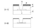
- a prepreg 3 and a copper foil 4 for upper layer wiring are laminated and integrated on the inner layer material 2 on which the inner layer wiring 1 is formed.
- a via hole 5 is provided by a laser.
- the prepreg 3 which is a resin film having a reinforcing base material such as glass fiber is used as the insulating layer 3 for bonding the inner layer material 2 and the copper foil 4 for upper layer wiring.
- a resin film such as a polymer epoxy resin or a thermoplastic polyimide adhesive film that does not have a reinforcing base and is used for a general multilayer wiring board can be used.
- the copper foil 4 is used as the metal foil 4 for the upper layer wiring.
- a nickel foil, an aluminum foil, a composite foil thereof, or the like used as a material for the multilayer wiring board is used. be able to.
- the method of laminating and integrating the prepreg and the copper foil on the upper layer on the inner layer material formed with wiring is a method of laminating and pressing the inner layer material and the prepreg, copper foil, or a method of laminating a resin film with a single-sided copper foil on the inner layer material Is used.
- the thickness of the insulating layer is about 10 to 100 ⁇ m, preferably 20 to 60 ⁇ m, and the thickness of the copper foil is 3 to 12 ⁇ m.
- the resin film with a single-sided copper foil in this case has a configuration in which a prepreg (resin film having a reinforcing base material) is disposed on the copper foil.
- a resin film that does not have a reinforcing substrate other than prepreg as the insulating layer a resin film such as a polymer epoxy resin or a thermoplastic polyimide adhesive film that does not have a reinforcing substrate is disposed on the copper foil. Is used.
- the copper foil and resin composition (resin varnish) used for the production of the resin film with a single-sided copper foil are the same as those used for general multilayer wiring boards.
- the resin varnish is heated and dried in order to bring the resin varnish into a B-stage state (semi-cured state). This condition is suitably 100 to 200 ° C.
- the residual solvent amount in the resin composition (resin varnish) after heating and drying is about 0.2 to 10% by mass. Is appropriate.
- vacuum or atmospheric pressure is suitable under conditions of 50 to 150 ° C. and 0.1 to 5 MPa.
- the blackening treatment layer formed on the copper foil for the upper wiring layer can be formed of a known layer formed for adhesion between the copper foil and the insulating layer in a general multilayer wiring board.
- Examples of such a blackening treatment layer include those formed by forming irregularities on the surface of the copper foil by copper oxide treatment or etching.
- CO 2 and CO is a solid-state laser of gas laser or a YAG or the like of an excimer like.
- a CO 2 laser can easily obtain a large output, and according to the direct laser method that has been developed in recent years, it is possible to process a hole for a via hole having a diameter of 50 ⁇ m or less.
- the copper foil for the upper wiring layer is etched with an etching solution such as ferric chloride aqueous solution, sodium persulfate, or sulfuric acid-hydrogen peroxide mixed solution.
- an etching solution such as ferric chloride aqueous solution, sodium persulfate, or sulfuric acid-hydrogen peroxide mixed solution.
- Half-etching is performed until the thickness of 4 reaches about 1 to 5 ⁇ m.
- the blackening treatment layer formed on the copper foil 4 is removed.
- an electroless copper plating layer 6 is formed.
- the activator Neogant made by Atotech Japan Co., Ltd., trade name; “Neogant” is a registered trademark
- HS201B manufactured by Hitachi Chemical Co., Ltd.
- a palladium colloid catalyst are used for imparting a catalyst nucleus. , Product name).
- Adsorption onto a copper foil of the palladium catalyst in the present embodiment is in the range of 0.03 ⁇ 0.6 ⁇ g / cm 2, more desirably, in the range of 0.05 ⁇ 0.3 ⁇ g / cm 2 .
- the treatment temperature for adsorbing the palladium catalyst is preferably 10 to 40 ° C. By controlling the treatment time, the adsorption amount of the palladium catalyst on the copper foil can be controlled.
- electroless copper plating layer For forming the electroless copper plating layer, commercially available electroless copper such as CUST2000 (manufactured by Hitachi Chemical Co., Ltd., trade name, “CUST” is a registered trademark) and CUST201 (trade name, manufactured by Hitachi Chemical Co., Ltd.).
- a plating solution can be used.
- These electroless copper plating solutions contain copper sulfate, formalin, complexing agent and sodium hydroxide as main components.
- the thickness of the electroless copper plating layer is not particularly limited as long as power can be supplied to form the next electrolytic filled copper plating layer, and is preferably in the range of 0.1 to 5 ⁇ m, more preferably 0.5. It is in the range of ⁇ 1.0 ⁇ m.
- the first electrolytic filled copper plating layer 7 is formed so as not to completely fill the via hole 5.
- the thickness of the electrolytic filled copper plating layer 7 is thicker than the thickness of the electrolytic filled copper plating layer 7 on the copper foil 4 for upper layer wiring.
- the thickness on the upper layer wiring copper foil 4 is in the range of 0.5 to 5.0 ⁇ m
- the thickness of the bottom surface in the via hole 5 is in the range of 2 to 20 ⁇ m.
- the copper foil for the upper wiring after etching with an etching solution such as ferric chloride aqueous solution, ammonium persulfate, or sulfuric acid-hydrogen peroxide mixed solution.
- an etching solution such as ferric chloride aqueous solution, ammonium persulfate, or sulfuric acid-hydrogen peroxide mixed solution.
- the via hole 5 is completely filled in the first electrolytic filled copper plating layer 7 or the electroless copper plating layer 6 whose surface has been etched.
- a second electrolytic filled copper plating layer 9 is formed.
- the inside of the via hole 5 is completely filled, and a portion on the via hole 5 that becomes the upper layer wiring 10 and a portion other than the via hole 5 become flat.
- copper sulfate electroplating for filled vias used in ordinary multilayer wiring boards can be used, and the first electrolytic filled plating solution in which the electrolytic plating layer 7 is formed may be used. It doesn't matter.
- the thickness of the plating is not particularly limited as long as it can be used as wiring and the via hole can be filled with a conductive metal, and is preferably in the range of 1 to 100 ⁇ m, and more preferably in the range of 10 to 50 ⁇ m.
- copper deposits thicker than the surface at the bottom of the via hole, so that the aspect when the second electrolytic filled copper plating 9 is embedded in the via hole is reduced.
- the etching solution is less likely to enter the via hole in the etching, the etching in the via hole is more difficult to etch than the surface layer, and the etching amount in the via hole is smaller than the etching amount in the surface layer. For this reason, since the diameter of the via hole is small and the depth to the bottom of the via hole is small, the diameter of the via hole is relatively small compared to the via hole having a large insulating layer. Can be suppressed.
- filling of the hole for the via hole by forming the electrolytic filled plating layer is performed twice, but the filling of the hole for the via hole is not limited to twice, and is divided into two or more times. You may do it.
- the electrolytic field on the metal foil for the via hole and the upper layer wiring previously formed is formed. If the plating layer is etched, voids can be similarly suppressed.
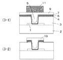
- an etching resist 11 having a thickness of 29 ⁇ m is formed using SL-1229 (Hitachi Chemical Co., Ltd., trade name) which is a dry film resist.
- the etching resist 11 is removed by development from the portions other than the portions on the via hole 5 and the upper layer wiring 10.
- step (3-2) of FIG. 3 after etching away portions other than the upper layer wiring 10, the etching resist 11 is stripped using an alkaline stripping solution, sulfuric acid, or a commercially available resist stripping solution, Upper layer wiring 10 is formed.
- a multilayer wiring board composed of two layers of the inner layer wiring 1 and the upper layer wiring 10 is completed.
- the surface of the upper layer wiring 10 of the multilayer wiring board is roughened and an insulating layer (not shown) formed on the upper wiring 10 is formed.
- the prepreg and a copper foil for upper layer wiring are laminated on the upper layer and the like while improving the adhesion.
- the inner layer material 2 on which the inner layer wiring 1 is formed has a resin film thickness of 30 ⁇ m and the copper foil 4 for the upper layer wiring.
- a resin film with a single-sided copper foil having a thickness of 5 ⁇ m is vacuum laminated under the conditions of 120 ° C. and 2 MPa.
- a blackened layer 8 having a thickness of 0.3 to 0.5 ⁇ m is formed on the surface of the copper foil 4 for upper layer wiring, and then a via hole hole with a diameter of 30 ⁇ m is formed by a direct laser method using a CO 2 laser. 5 is processed.
- the copper foil for upper wiring is blackened by an etching solution such as ferric chloride aqueous solution, ammonium persulfate, or sulfuric acid-hydrogen peroxide mixed solution.
- an etching solution such as ferric chloride aqueous solution, ammonium persulfate, or sulfuric acid-hydrogen peroxide mixed solution.
- half etching is performed until the copper foil thickness becomes 2 to 3 ⁇ m.
- step (2-1) in FIG. 2 catalyst nuclei are formed on the copper foil and inside the via hole using HS201B (trade name, manufactured by Hitachi Chemical Co., Ltd.) which is a palladium colloid catalyst.
- HS201B trade name, manufactured by Hitachi Chemical Co., Ltd.
- CUST2000 trade name, manufactured by Hitachi Chemical Co., Ltd., “CUST” is a registered trademark.
- the first electrolytic filled copper plating layer has a thickness of 5 ⁇ m on the upper layer copper foil and a thickness of 15 ⁇ m on the bottom surface in the via hole.
- the electrolytic plating solution a commercially available direct current electrolytic plating solution CU-BRITE VFIV (manufactured by JCU Corporation, trade name) was used.
- step (2-3) of FIG. 2 the film thickness of the electrolytic filled copper plating layer on the copper foil for the upper wiring layer is reduced by the etching solution of ammonium persulfate and sulfuric acid-hydrogen peroxide aqueous solution.
- the electrolytic filled copper plating layer is removed by etching until the thickness becomes 2 ⁇ m.
- via holes are filled with a second electrolytic filled copper plating layer having a thickness of 20 ⁇ m on the upper layer copper foil.
- the electrolytic plating solution used for forming the second electrolytic filled copper plating layer the same solution as that of the first electrolytic plating solution was used.
- step (3-1) in FIG. 3 an etching resist having a thickness of 29 ⁇ m is formed using SL-1229 (trade name, Hitachi Chemical Co., Ltd.) which is a dry film resist.
- the etching resist is removed from the portions other than those on the via hole and the upper layer wiring.
- step (3-2) of FIG. 3 after etching away copper other than the upper wiring, etching resist is stripped using an alkaline stripping solution, sulfuric acid, or a commercially available resist stripping solution, Upper layer wiring is formed.
- Example 2 First, as shown in step (1-1) of FIG. 1, the thickness of the resin film serving as the insulating layer is 30 ⁇ m on the inner layer material on which the inner layer wiring is formed, and the thickness of the copper foil serving as the copper foil for the upper layer wiring is A resin film with a single-sided copper foil of 5 ⁇ m is vacuum laminated under the conditions of 120 ° C. and 2 MPa. Next, after forming a blackening treatment layer 8 having a thickness of 0.3 to 0.5 ⁇ m on the surface of the copper foil for the upper layer wiring, a via hole for a diameter of 30 ⁇ m is processed by a direct laser method using a CO 2 laser. To do.
- the copper foil for upper wiring is blackened by an etching solution such as ferric chloride aqueous solution, ammonium persulfate, or sulfuric acid-hydrogen peroxide mixed solution.
- an etching solution such as ferric chloride aqueous solution, ammonium persulfate, or sulfuric acid-hydrogen peroxide mixed solution.
- half etching is performed until the copper foil thickness becomes 2 to 3 ⁇ m.
- step (2-1) in FIG. 2 catalyst nuclei are formed on the copper foil and inside the via hole using HS201B (trade name, manufactured by Hitachi Chemical Co., Ltd.) which is a palladium colloid catalyst.
- HS201B trade name, manufactured by Hitachi Chemical Co., Ltd.
- CUST2000 trade name, manufactured by Hitachi Chemical Co., Ltd., “CUST” is a registered trademark.
- the first electrolytic filled copper plating layer having a thickness of 2 ⁇ m on the upper-layer wiring copper foil and a thickness of 3 ⁇ m on the bottom surface in the via-hole hole is obtained.
- the electrolytic plating solution a commercially available direct current electrolytic plating solution CU-BRITE VFIV (manufactured by JCU Corporation, trade name) was used.
- the film thickness of the electrolytic filled copper plating layer on the copper foil for upper wiring is 1.5 ⁇ m by an etching solution in which sodium persulfate and sulfuric acid are mixed. Until the electrolytic filled copper plating layer is removed by etching.
- via holes are filled with a second electrolytic filled copper plating layer having a thickness of 20 ⁇ m on the upper layer copper foil.
- the electrolytic plating solution used for forming the second electrolytic filled copper plating layer the same solution as that of the first electrolytic plating solution was used.
- step (3-1) in FIG. 3 an etching resist having a thickness of 29 ⁇ m is formed using SL-1229 (trade name, Hitachi Chemical Co., Ltd.) which is a dry film resist.
- the etching resist is removed from the portions other than those on the via hole and the upper layer wiring.
- step (3-2) of FIG. 3 after etching away copper other than the upper wiring, etching resist is stripped using an alkaline stripping solution, sulfuric acid, or a commercially available resist stripping solution, Upper layer wiring is formed.
- the thickness of the resin film serving as the insulating layer is 30 ⁇ m on the inner layer material on which the inner layer wiring is formed, and the thickness of the copper foil serving as the copper foil for the upper layer wiring is A resin film with a single-sided copper foil of 5 ⁇ m is vacuum laminated under the conditions of 120 ° C. and 2 MPa.
- a blackening treatment layer 8 having a thickness of 0.3 to 0.5 ⁇ m on the copper foil surface of the upper wiring layer, a via hole for a diameter of 30 ⁇ m is processed by a direct laser method using a CO 2 laser. To do.
- the copper foil for upper wiring is blackened by an etching solution such as ferric chloride aqueous solution, ammonium persulfate, or sulfuric acid-hydrogen peroxide mixed solution.
- an etching solution such as ferric chloride aqueous solution, ammonium persulfate, or sulfuric acid-hydrogen peroxide mixed solution.
- half etching is performed until the copper foil thickness becomes 2 to 3 ⁇ m.
- step (2-1) in FIG. 2 catalyst nuclei are formed on the copper foil and inside the via hole using HS201B (trade name, manufactured by Hitachi Chemical Co., Ltd.) which is a palladium colloid catalyst.
- HS201B trade name, manufactured by Hitachi Chemical Co., Ltd.
- CUST2000 trade name, manufactured by Hitachi Chemical Co., Ltd., “CUST” is a registered trademark.
- an electrolytic filled copper plating layer having a thickness of 20 ⁇ m is formed on the copper foil for the upper layer wiring.
- the first electrolytic filled copper plating layer was formed so as to flatten the portions other than the via hole for the upper layer wiring and the via hole.
- a commercially available DC electrolytic plating solution CU-BRITE VFIV manufactured by JCU Corporation, trade name was used.
- step (3-1) in FIG. 3 an etching resist having a thickness of 29 ⁇ m is formed using SL-1229 (trade name, Hitachi Chemical Co., Ltd.), which is a dry film resist.
- the etching resist is removed from the portions other than those on the via hole and the layer wiring.
- step (3-2) of FIG. 3 after etching away copper other than the upper layer wiring, the etching resist is stripped using an alkaline stripping solution, sulfuric acid, or a commercially available resist stripping solution. Form wiring.
- Table 1 summarizes the occurrence frequency of plating voids in Examples 1 and 2 and Comparative Example.
- the void generation frequency was 0, and the via hole could be filled.
- the comparative example void generation was almost 100%.
- the present invention can provide a method for manufacturing a multilayer wiring board capable of suppressing plating voids of an electrolytic filled plating layer even for a hole for a via hole having a diameter comparable to the insulating layer thickness, it is industrially effective. It is.
- Inner layer wiring 2. Inner layer material 3. prepreg or insulating layer 4. Metal foil or copper foil 5. Hole for via hole 6. Electroless plating layer or electroless copper plating layer 7. First electrolytic filled plating layer or first electrolytic filled copper plating layer Blackening layer 9. 9. Second electrolytic filled plating layer or second electrolytic filled copper plating layer 10. Upper layer wiring Etching resist
Landscapes
- Chemical & Material Sciences (AREA)
- Engineering & Computer Science (AREA)
- Organic Chemistry (AREA)
- Chemical Kinetics & Catalysis (AREA)
- Materials Engineering (AREA)
- Metallurgy (AREA)
- Electrochemistry (AREA)
- Microelectronics & Electronic Packaging (AREA)
- Manufacturing & Machinery (AREA)
- General Chemical & Material Sciences (AREA)
- Mechanical Engineering (AREA)
- Production Of Multi-Layered Print Wiring Board (AREA)
- Printing Elements For Providing Electric Connections Between Printed Circuits (AREA)
- Electroplating Methods And Accessories (AREA)
Abstract
Description
1. 内層配線を形成した内層材と絶縁層と上層配線用の金属箔とを積層一体化し、前記上層配線用の金属箔及び絶縁層に、前記上層配線用の金属箔から内層配線に到るビアホール用穴を設ける工程(1)と、前記ビアホール用穴内及び上層配線用の金属箔上に、下地無電解めっき層を形成した後、電解フィルドめっき層を形成することによって前記ビアホール用穴を穴埋めし、前記上層配線用金属箔と内層配線とを接続するビアホールを形成する工程(2)と、前記電解フィルドめっき層を形成後の上層配線用金属箔を配線形成して、上層配線を形成する工程(3)と、を有する多層配線基板の製造方法であって、前記工程(2)における、電解フィルドめっき層の形成によるビアホール用穴の穴埋めが、二度以上に分けて行われ、前記二度目以降のそれぞれの電解フィルドめっき層の形成の前に、先に形成したビアホール用穴内及び上層配線用の金属箔上の電解フィルドめっき層をエッチングする工程を有する多層配線基板の製造方法。
2. 項1において、工程(2)が、ビアホール用穴内及び上層配線用の金属箔上に、下地無電解めっき層を形成する工程(2-1)と、ビアホール用穴を完全に穴埋めしない程度の一度目の電解フィルドめっき層を形成する工程(2-2)と、前記工程(2-2)で形成した一度目の電解フィルドめっき層の表面をエッチングする工程(2-3)と、前記工程(2-3)で表面がエッチングされた一度目の電解フィルドめっき層上に、前記ビアホール用穴を完全に穴埋めする二度目の電解フィルドめっき層を形成する工程(2-4)と、を有する多層配線基板の製造方法。
3. 項1の二回目以降のそれぞれの電解フィルドめっき層の形成の前に、その直前に形成した電解フィルドめっき層の表面をエッチングする工程、又は請求項2の工程(2-3)において、先に形成された上層配線用の金属箔上の電解フィルドめっき層の厚さが、少なくとも半分以下になるまで、エッチングする多層配線基板の製造方法。
まず、図1の工程(1-1)に示すように、内層配線1を形成した内層材2に、絶縁層3となる樹脂フィルムの厚みが30μmで、上層配線用の銅箔4となる銅箔4の厚みが5μmの片面銅箔付樹脂フィルムを、120℃、2MPaの条件で真空ラミネートする。次に、この上層配線用の銅箔4の表面に、厚さ0.3~0.5μmの黒化処理層8を形成した後、CO2レーザによるダイレクトレーザ工法により、直径30μmのビアホール用穴5を加工する。
まず、図1の工程(1-1)に示すように、内層配線を形成した内層材に、絶縁層となる樹脂フィルムの厚みが30μmで、上層配線用の銅箔となる銅箔の厚みが5μmの片面銅箔付樹脂フィルムを、120℃、2MPaの条件で真空ラミネートする。次に、この上層配線用の銅箔表面に、厚さ0.3~0.5μmの黒化処理層8を形成した後、CO2レーザによるダイレクトレーザ工法により、直径30μmのビアホール用穴を加工する。
まず、図1の工程(1-1)に示すように、内層配線を形成した内層材に、絶縁層となる樹脂フィルムの厚みが30μmで、上層配線用の銅箔となる銅箔の厚みが5μmの片面銅箔付樹脂フィルムを、120℃、2MPaの条件で真空ラミネートする。次に、この上層配線層の銅箔表面に、厚さ0.3~0.5μmの黒化処理層8を形成した後、CO2レーザによるダイレクトレーザ工法により、直径30μmのビアホール用穴を加工する。

2.内層材
3.プリプレグ又は絶縁層
4.金属箔又は銅箔
5.ビアホール用穴
6.無電解めっき層又は無電解銅めっき層
7.一度目の電解フィルドめっき層又は一度目の電解フィルド銅めっき層
8.黒化処理層
9.二度目の電解フィルドめっき層又は二度目の電解フィルド銅めっき層
10.上層配線
11.エッチングレジスト
Claims (3)
- 内層配線を形成した内層材と絶縁層と上層配線用の金属箔とを積層一体化し、前記上層配線用の金属箔及び絶縁層に、前記上層配線用の金属箔から内層配線に到るビアホール用穴を設ける工程(1)と、
前記ビアホール用穴内及び上層配線用の金属箔上に、下地無電解めっき層を形成した後、電解フィルドめっき層を形成することによって前記ビアホール用穴を穴埋めし、前記上層配線用金属箔と内層配線とを接続するビアホールを形成する工程(2)と、
前記電解フィルドめっき層を形成後の上層配線用金属箔を配線形成して、上層配線を形成する工程(3)と、
を有する多層配線基板の製造方法であって、
前記工程(2)における、電解フィルドめっき層の形成によるビアホール用穴の穴埋めが、二度以上に分けて行われ、
前記二度目以降のそれぞれの電解フィルドめっき層の形成の前に、先に形成したビアホール用穴内及び上層配線用の金属箔上の電解フィルドめっき層をエッチングする工程を有する多層配線基板の製造方法。 - 請求項1において、
工程(2)が、
ビアホール用穴内及び上層配線用の金属箔上に、下地無電解めっき層を形成する工程(2-1)と、
ビアホール用穴を完全に穴埋めしない程度の一度目の電解フィルドめっき層を形成する工程(2-2)と、
前記工程(2-2)で形成した一度目の電解フィルドめっき層の表面をエッチングする工程(2-3)と、
前記工程(2-3)で表面がエッチングされた一度目の電解フィルドめっき層上に、前記ビアホール用穴を完全に穴埋めする二度目の電解フィルドめっき層を形成する工程(2-4)と、
を有する多層配線基板の製造方法。 - 請求項1の二回目以降のそれぞれの電解フィルドめっき層の形成の前に、その直前に形成した電解フィルドめっき層の表面をエッチングする工程、又は請求項2の工程(2-3)において、
先に形成された上層配線用の金属箔上の電解フィルドめっき層の厚さが、少なくとも半分以下になるまで、エッチングする多層配線基板の製造方法。
Priority Applications (2)
| Application Number | Priority Date | Filing Date | Title |
|---|---|---|---|
| US14/778,677 US9516764B2 (en) | 2013-03-28 | 2014-03-25 | Method for manufacturing multilayer wiring substrate |
| CN201480018681.2A CN105075411B (zh) | 2013-03-28 | 2014-03-25 | 多层配线基板的制造方法 |
Applications Claiming Priority (2)
| Application Number | Priority Date | Filing Date | Title |
|---|---|---|---|
| JP2013069058A JP6241641B2 (ja) | 2013-03-28 | 2013-03-28 | 多層配線基板の製造方法 |
| JP2013-069058 | 2013-03-28 |
Publications (1)
| Publication Number | Publication Date |
|---|---|
| WO2014157206A1 true WO2014157206A1 (ja) | 2014-10-02 |
Family
ID=51624175
Family Applications (1)
| Application Number | Title | Priority Date | Filing Date |
|---|---|---|---|
| PCT/JP2014/058291 Ceased WO2014157206A1 (ja) | 2013-03-28 | 2014-03-25 | 多層配線基板の製造方法 |
Country Status (4)
| Country | Link |
|---|---|
| US (1) | US9516764B2 (ja) |
| JP (1) | JP6241641B2 (ja) |
| CN (1) | CN105075411B (ja) |
| WO (1) | WO2014157206A1 (ja) |
Families Citing this family (10)
| Publication number | Priority date | Publication date | Assignee | Title |
|---|---|---|---|---|
| JP6508589B2 (ja) | 2014-10-24 | 2019-05-08 | 住友電工プリントサーキット株式会社 | フレキシブルプリント配線板及びその製造方法 |
| US11781236B2 (en) * | 2017-11-10 | 2023-10-10 | Namics Corporation | Composite copper foil |
| JP2019123637A (ja) * | 2018-01-16 | 2019-07-25 | 日立化成株式会社 | 接合材 |
| CN113994770B (zh) * | 2019-05-31 | 2024-09-10 | 凸版印刷株式会社 | 多层配线基板及其制造方法 |
| CN111107714A (zh) * | 2020-01-15 | 2020-05-05 | 广东科翔电子科技股份有限公司 | 一种任意层互连hdi内层芯板盲孔的制作方法 |
| CN111654978B (zh) * | 2020-06-30 | 2021-03-30 | 景旺电子科技(珠海)有限公司 | 一种电路板制作方法 |
| WO2022264378A1 (ja) * | 2021-06-17 | 2022-12-22 | 昭和電工マテリアルズ株式会社 | 配線基板の製造方法及び積層板 |
| CN116209165A (zh) * | 2021-12-01 | 2023-06-02 | 奥特斯(中国)有限公司 | 制造部件承载件的方法和部件承载件 |
| US20250063651A1 (en) * | 2022-01-04 | 2025-02-20 | Sumitomo Electric Industries, Ltd. | Printed wiring board and method of manufacturing printed wiring board |
| US12543273B2 (en) * | 2022-09-28 | 2026-02-03 | Ibiden Co., Ltd. | Printed wiring board |
Citations (3)
| Publication number | Priority date | Publication date | Assignee | Title |
|---|---|---|---|---|
| JPH11298141A (ja) * | 1998-04-08 | 1999-10-29 | Hitachi Ltd | 電子装置の製造方法 |
| JP2000269644A (ja) * | 1999-03-15 | 2000-09-29 | Matsushita Electric Works Ltd | ビルドアップ多層配線板の製造方法 |
| JP2008021770A (ja) * | 2006-07-12 | 2008-01-31 | Matsushita Electric Ind Co Ltd | 基板およびその製造方法 |
Family Cites Families (14)
| Publication number | Priority date | Publication date | Assignee | Title |
|---|---|---|---|---|
| DE69803543T2 (de) * | 1997-05-07 | 2002-09-05 | Koninklijke Philips Electronics N.V., Eindhoven | Bildprojektionssystem |
| EP2086299A1 (en) * | 1999-06-02 | 2009-08-05 | Ibiden Co., Ltd. | Multi-layer printed circuit board and method of manufacturing multi-layer printed circuit board |
| JP2002252446A (ja) * | 2001-02-23 | 2002-09-06 | Sony Chem Corp | フレキシブル配線基板の製造方法 |
| JP2003318544A (ja) | 2002-04-22 | 2003-11-07 | Toppan Printing Co Ltd | 多層配線基板およびその製造方法 |
| JP3937993B2 (ja) * | 2002-10-02 | 2007-06-27 | 日立電線株式会社 | 配線板の製造方法 |
| US20080029400A1 (en) * | 2005-05-13 | 2008-02-07 | Stephen Mazur | Selective electroplating onto recessed surfaces |
| WO2007012104A1 (de) * | 2005-07-29 | 2007-02-01 | Karl Deininger | Verfahren und vorrichtung zur verbindung zweier materialbahnen |
| TW200746940A (en) * | 2005-10-14 | 2007-12-16 | Ibiden Co Ltd | Printed wiring board |
| CN103444275A (zh) * | 2007-06-15 | 2013-12-11 | 美录德有限公司 | 印刷电路板制造用的镀铜填充方法以及使用该镀铜填充方法得到的印刷电路板 |
| US8232655B2 (en) * | 2008-01-03 | 2012-07-31 | International Business Machines Corporation | Bump pad metallurgy employing an electrolytic Cu / electorlytic Ni / electrolytic Cu stack |
| US7879720B2 (en) * | 2008-09-30 | 2011-02-01 | Samsung Electronics Co., Ltd. | Methods of forming electrical interconnects using electroless plating techniques that inhibit void formation |
| JP5565950B2 (ja) * | 2010-08-23 | 2014-08-06 | 京セラSlcテクノロジー株式会社 | 配線基板の製造方法 |
| EP2566311A1 (en) * | 2011-09-02 | 2013-03-06 | Atotech Deutschland GmbH | Direct plating method |
| JP5823359B2 (ja) * | 2012-08-23 | 2015-11-25 | 株式会社東芝 | 半導体装置の製造方法 |
-
2013
- 2013-03-28 JP JP2013069058A patent/JP6241641B2/ja active Active
-
2014
- 2014-03-25 US US14/778,677 patent/US9516764B2/en active Active
- 2014-03-25 CN CN201480018681.2A patent/CN105075411B/zh active Active
- 2014-03-25 WO PCT/JP2014/058291 patent/WO2014157206A1/ja not_active Ceased
Patent Citations (3)
| Publication number | Priority date | Publication date | Assignee | Title |
|---|---|---|---|---|
| JPH11298141A (ja) * | 1998-04-08 | 1999-10-29 | Hitachi Ltd | 電子装置の製造方法 |
| JP2000269644A (ja) * | 1999-03-15 | 2000-09-29 | Matsushita Electric Works Ltd | ビルドアップ多層配線板の製造方法 |
| JP2008021770A (ja) * | 2006-07-12 | 2008-01-31 | Matsushita Electric Ind Co Ltd | 基板およびその製造方法 |
Also Published As
| Publication number | Publication date |
|---|---|
| CN105075411A (zh) | 2015-11-18 |
| US9516764B2 (en) | 2016-12-06 |
| JP6241641B2 (ja) | 2017-12-06 |
| JP2014192483A (ja) | 2014-10-06 |
| US20160050769A1 (en) | 2016-02-18 |
| CN105075411B (zh) | 2018-11-16 |
Similar Documents
| Publication | Publication Date | Title |
|---|---|---|
| JP6241641B2 (ja) | 多層配線基板の製造方法 | |
| JP6350062B2 (ja) | 多層配線基板の製造方法 | |
| JP6350064B2 (ja) | 多層配線基板の製造方法 | |
| JP6641717B2 (ja) | 多層配線基板の製造方法 | |
| US10165691B2 (en) | Method for manufacturing multilayer wiring substrate | |
| CN103039131B (zh) | 印刷布线板的制造方法以及印刷布线板 | |
| JP7608310B2 (ja) | 回路基板の製造方法 | |
| JP2010153628A (ja) | 多層配線基板の製造方法 | |
| JP5051443B2 (ja) | 多層配線基板の製造方法 | |
| JP5077662B2 (ja) | 多層配線基板の製造方法 | |
| KR101061243B1 (ko) | 인쇄회로기판 및 그 제조방법 | |
| WO2015053082A1 (ja) | 多層配線基板及びその製造方法 | |
| KR20120009114A (ko) | 인쇄회로기판 및 인쇄회로기판 제조방법 | |
| JP2008010517A (ja) | プリプレグとフレキシブルリジット配線板の製造方法 | |
| JP2015220393A (ja) | 回路形成用支持基板、それを用いたプリント配線板、及びその製造方法 |
Legal Events
| Date | Code | Title | Description |
|---|---|---|---|
| WWE | Wipo information: entry into national phase |
Ref document number: 201480018681.2 Country of ref document: CN |
|
| 121 | Ep: the epo has been informed by wipo that ep was designated in this application |
Ref document number: 14775936 Country of ref document: EP Kind code of ref document: A1 |
|
| WWE | Wipo information: entry into national phase |
Ref document number: 14778677 Country of ref document: US |
|
| NENP | Non-entry into the national phase |
Ref country code: DE |
|
| 122 | Ep: pct application non-entry in european phase |
Ref document number: 14775936 Country of ref document: EP Kind code of ref document: A1 |