WO2014156441A1 - カメラモジュールの製造方法、カメラモジュール及び携帯端末 - Google Patents
カメラモジュールの製造方法、カメラモジュール及び携帯端末 Download PDFInfo
- Publication number
- WO2014156441A1 WO2014156441A1 PCT/JP2014/054620 JP2014054620W WO2014156441A1 WO 2014156441 A1 WO2014156441 A1 WO 2014156441A1 JP 2014054620 W JP2014054620 W JP 2014054620W WO 2014156441 A1 WO2014156441 A1 WO 2014156441A1
- Authority
- WO
- WIPO (PCT)
- Prior art keywords
- camera module
- circuit board
- synthetic resin
- solder
- flux
- Prior art date
- Legal status (The legal status is an assumption and is not a legal conclusion. Google has not performed a legal analysis and makes no representation as to the accuracy of the status listed.)
- Ceased
Links
Images


Classifications
-
- H—ELECTRICITY
- H04—ELECTRIC COMMUNICATION TECHNIQUE
- H04N—PICTORIAL COMMUNICATION, e.g. TELEVISION
- H04N23/00—Cameras or camera modules comprising electronic image sensors; Control thereof
- H04N23/57—Mechanical or electrical details of cameras or camera modules specially adapted for being embedded in other devices
-
- H—ELECTRICITY
- H04—ELECTRIC COMMUNICATION TECHNIQUE
- H04N—PICTORIAL COMMUNICATION, e.g. TELEVISION
- H04N23/00—Cameras or camera modules comprising electronic image sensors; Control thereof
- H04N23/60—Control of cameras or camera modules
- H04N23/62—Control of parameters via user interfaces
Definitions
- the present invention relates to a method for manufacturing a small camera module using an image sensor such as a CCD image sensor or a CMOS image sensor, a camera module, and a portable terminal using such a camera module.
- an image sensor such as a CCD image sensor or a CMOS image sensor
- a camera module and a portable terminal using such a camera module.
- solder paste for cleaning the oxide.
- the flux quickly wraps around the surface of the terminal, and has a function of improving conductivity by removing the oxide.
- the rosin-based flux that is generally used covers the solder surface after soldering and solidifies and remains as a residue.
- the flux residue piece that has been peeled off is dropped and attached to the image pickup surface of the image pickup device, it is recognized as a black spot on the subject image, leading to deterioration in image quality.
- this problem often occurs due to vibration, impact, etc. during use after the camera module is mounted on a device such as a portable terminal, and cannot be selected as a defective product during the manufacturing process.
- flux loses its function after soldering, so it is possible to remove the flux from the chip parts by cleaning, but it requires a cleaning facility and adds a cleaning process, which increases costs. This is not preferable.
- Patent Document 1 in order to prevent the solder paste or flux residue for mounting the chip component from being peeled off by vibration or impact and attached to the image sensor, a space for sealing the image sensor, There is disclosed a camera module in which a chip component storage space for storing a chip component and its peripheral region is formed, and both spaces are isolated.
- the image pickup device and the chip component are separated by a dust-proof wall, thereby preventing the solder paste and the flux residue peeled from the chip component from reaching the image pickup device. If a dust-proof wall is provided between the image sensor and the chip component, the circuit board must be enlarged accordingly, and there is a problem that the camera module is increased in size.
- the present invention has been made in view of such problems, and while being small in size, it is possible to suppress the adhesion of flux residue pieces to the imaging surface of the imaging device, and to improve the impact resistance while improving the image quality. It is an object of the present invention to provide a method for manufacturing a camera module capable of forming an image, a camera module, and a portable terminal using the camera module.
- a method of manufacturing a camera module includes an imaging lens that forms a subject image, an imaging device that photoelectrically converts a subject image formed by the imaging lens, a circuit board on which the imaging device and chip components are mounted,
- a method of manufacturing a camera module comprising: mounting the chip component on the circuit board; mounting the imaging element on the circuit board; and mounting a pedestal member and / or the imaging lens on the circuit board. And a step of mounting the chip component on the circuit board, wherein the chip component is connected to the circuit board using a solder paste mixed with a synthetic resin flux.
- a camera module includes an imaging lens that forms a subject image, an imaging device that photoelectrically converts a subject image formed by the imaging lens, and a circuit board on which the imaging device and chip components are mounted.
- the chip component mounted on the circuit board is connected to the circuit board using a solder paste mixed with a synthetic resin flux.
- a chip component is connected to a circuit board using a solder paste mixed with a synthetic resin flux, so that a certain degree of elasticity is obtained after the residue of the synthetic resin flux covers and solidifies the solder. Therefore, even if an impact is applied, it is possible to prevent the flux residue pieces from being peeled and scattered, thereby preventing the image pickup device mounted on the same circuit board from being contaminated. Further, it is not necessary to provide a dust-proof wall and the like, and the camera module can be reduced in size. In addition, since many chip components are 1 mm or less in length, the area of the soldered part is small, so it may peel off when subjected to a strong impact, but the chip component should be covered with a synthetic resin flux residue.
- the connectivity with the circuit board can be enhanced to prevent the chip components from falling off, thereby improving the impact resistance.
- a synthetic resin-based flux residue moisture permeability is suppressed and the reliability of the chip component is enhanced.
- the flux is a flux used in the atmosphere (at atmospheric pressure, in the presence of oxygen) together with a brazing material such as a solder or a low-melting-point metal, which is used when an electrical connection structure, particularly metals are joined together. Flux is used for the purpose of improving the spreadability of the brazing material and preventing metal oxidation on the joint surface by removing foreign matters such as oxides on the joint surface and further reducing the interfacial tension with the joint member.
- the synthetic resin flux for example, the product name M705-GRN360-S2 of Senju Metal Industry Co., Ltd., the product name TLF-204-GTS-VR1 of Tamura Seisakusho Co., Ltd. can be preferably used.
- the flux is classified into resin-based, organic acid-based, and inorganic acid-based ones.
- resin-based ones rosin is the main ingredient
- modified rosin is the main ingredient
- synthetic resin is the main ingredient.
- the present invention is to use a solder paste in which a flux mainly composed of a synthetic resin is mixed.
- a portable terminal includes the above-described camera module, and a display unit that displays a subject image obtained by the camera module and / or a wireless communication unit that transmits a subject image obtained by the camera module. It is characterized by.
- a camera module that can form a high-quality image while reducing the adhesion of flux residue pieces to the imaging surface of the imaging device and improving impact resistance while being small, and the camera module.
- the used mobile terminal can be provided.
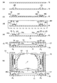
- FIG. 6 is a diagram showing camera module manufacturing steps (a) to (g). It is the front view (a) of the smart phone which mounts a camera module, and the back view (b) of the smart phone which applied the camera module. It is a control block diagram of the smart phone of FIG. It is an expansion schematic diagram which shows the chip component of a comparative example. It is an expansion schematic diagram which shows the chip component of an Example.
- FIG. 1 is a cross-sectional view of a camera module 10 according to the present embodiment.
- FIG. 1 is a schematic diagram, and some shapes, dimensions, and the like are different from actual ones.
- a camera module 10 includes a CMOS image sensor 11 as a solid-state image sensor having a photoelectric conversion unit 11a, and an imaging lens 12 that forms a subject image on the photoelectric conversion unit 11a of the image sensor 11.
- the lens barrel 13 holding the imaging lens 12, the parallel plate-shaped optical filter 14 composed of an IR cut filter and / or a low-pass filter, the actuator 15 for driving the imaging lens 12, the imaging element 11 and the circuit
- the circuit board 16 on which the chip component 18 is mounted and the base member 17 that holds the imaging lens 12 and the actuator 15 are included.
- the chip component refers to a chip resistor, a chip capacitor, a chip inductor, and the like, for example, 3216 size (3.2 mm ⁇ 1.6 mm), 2012 size (2.0 mm ⁇ 1.2 mm), 1608 size (1. 6 mm ⁇ 0.8 mm), 1005 size (1.0 mm ⁇ 0.5 mm), 0603 size (0.6 mm ⁇ 0.3 mm), 0402 size (0.4 mm ⁇ 0.2 mm), and the like.
- the imaging device 11 is formed with a photoelectric conversion unit 11a as an imaging surface in which a plurality of light receiving pixels (photoelectric conversion devices) are two-dimensionally arranged on a wafer 11b.
- a signal processing circuit (not shown).
- Such a signal processing circuit includes a driving circuit unit that sequentially drives each pixel to obtain an output signal, an A / D conversion unit that converts each output signal into a digital signal, and a signal that forms an image signal output using the digital signal. It consists of a processing unit and the like.
- a plurality of pads (not shown) formed near the outer edge of the wafer 11b of the image sensor 11 on the light receiving surface side are connected to the circuit board 16 by wires 11c.
- a wiring pattern for processing a signal output from the imaging element 11 is formed around the imaging element 11, and a chip component 18 is mounted on the wiring pattern by solder. .
- the pedestal member 17 integrally formed of resin has a generally rectangular parallelepiped housing shape, and includes four side wall portions 17a provided so as to surround the image pickup device 11 and an upper wall portion 17b intersecting with the upper end thereof. Have. A rectangular opening 17c is formed at the center of the upper wall portion 17b, and the optical filter 14 is attached to the upper wall portion 17b so as to cover the opening 17c. That is, the image sensor 11 and the chip component 18 are sealed in the same space by the base member 17 to which the optical filter 14 is fixed.
- the image sensor 11 converts an output signal from the photoelectric conversion unit 11a into an image signal such as a digital YUV signal, and an external circuit (for example, a camera module) (not shown) is connected from the wire 11c through the wiring pattern of the circuit board 16. To the control circuit of the higher-level device mounted). Further, it is also possible to receive power and a clock signal for driving the image pickup device 11 from an external circuit through the wire 11c from the wiring pattern of the circuit board 16.
- Y is a luminance signal
- the image sensor is not limited to the above CMOS image sensor, and other devices such as a CCD may be used.
- an imaging lens 12 is provided inside the lens barrel 13.
- the actuator 15 includes a cylindrical carrier 15a screwed to the lens barrel 13, a coil 15b attached to the carrier 15a and extending in the optical axis direction, a magnet 15c disposed facing the coil 15b, and a magnet 15c. And a housing-like yoke 15d that supports The coil 15b is connected to an external circuit via a wiring (not shown). The lower end of the yoke 15d is bonded onto the upper wall portion 17b of the base member 17.
- the carrier 15a is urged toward the image pickup device 11 by an elastic member (not shown).
- FIG. 2 (a) to 2 (g) are diagrams showing a manufacturing process of the camera module 10, and some of the components are simplified.
- a circuit board 16 having a wiring pattern printed on the surface is arranged, and as shown in FIG. 2 (b), a solder paste is formed along the wiring pattern on the circuit board 16.
- Apply HP is applied.
- the solder paste HP contains granular solder mixed in a synthetic resin flux containing an acrylic resin, and is applied by a method such as screen printing.
- the chip component 18 is placed on the solder paste HP and inserted into the reflow furnace RF as shown in FIG. (For example, in the case of general Sn-3AG-0.5Cu, 220 ° C. or higher). Then, first, the synthetic resin-based flux in the solder paste HP is developed on the chip component 18 and the wiring pattern, and after the oxide is washed, the granular solder in the solder paste HP is melted and then discharged from the reflow furnace RF. Cool and solidify. At this time, the synthetic resin-based flux residue FL coats the periphery of the solidified solder HD, but the synthetic resin-based flux residue FL does not lose its elasticity even when solidified, so that it may peel off itself. There is also a function of protecting the solder HD and the chip component 18 from falling off when an impact is applied. In addition, the soldered chip component 18 and the terminal of the wiring pattern can also be coated with the synthetic resin-based flux residue FL, thereby improving the moisture resistance.
- the image pickup device 11 is placed and fixed on the circuit board 16 on which the chip component 18 is mounted, and connected by bonding with a wire 11c.
- a base member 17 having the optical filter 14 attached thereto is adhered to the circuit board 16, and the imaging lens 12 and the base member 17 are placed on the base member 17 as shown in FIG. 2 (g).
- the actuator 15 holding the lens barrel 13 is placed and fixed with an adhesive.
- the camera module 10 is completed.
- the pedestal member 17 is assembled to the circuit board 16 and the imaging lens is assembled to the pedestal member 17.
- the present invention is not limited to this, and the pedestal member 17 is omitted and the imaging lens is attached to the circuit board 16. May be assembled.
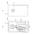
- FIG. 3A and 3B show a state where the camera module 10 is mounted on a smartphone 100 that is an example of a mobile terminal.
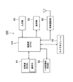
- FIG. 4 is a control block diagram of the smartphone 100.
- the object side end surface of the lens barrel 13 is provided on the back surface of the smartphone 100 (see FIG. 3B), and a liquid crystal display unit is disposed on the surface side of the smartphone 100.
- the camera module 10 is connected to the control unit 101 of the smartphone 100 via an external connection terminal (an arrow in FIG. 4), and outputs an image signal such as a luminance signal or a color difference signal to the control unit 101 side.
- the smartphone 100 performs overall control of each unit, and a control unit (CPU) 101 that executes a program corresponding to each process, a switch such as a power source, a number, and the like using a touch pad.
- a control unit CPU
- a switch such as a power source, a number, and the like using a touch pad.
- ROM storage unit
- the camera module 10 is operated by the operation of the input unit 60 of the smartphone 100.
- the camera module 10 is operated by driving the imaging lens 12 by the actuator 15 to perform an autofocus operation and pressing the release button 71 or the like. Imaging.
- the image signal input from the camera module 10 is stored in the storage unit 91 or the temporary storage unit 92 by the control system of the smartphone 100 or displayed on the display unit 65, and further via the wireless communication unit 80. It is transmitted to the outside as video information.
- a camera module is manufactured in the manufacturing process shown in FIG. 2, and the solder paste having a general rosin-based flux is used.
- a camera module was manufactured in the manufacturing process shown in FIG. Of these, 1,000 camera modules that passed image inspection were prepared.
- This camera module was placed on a resin tray, dropped from a height of 1 m on the floor toward the floor, and an impact test was conducted.
- the floor is concrete. Further, after the test, the image inspection was performed again to count image defects. And the component adhering to the imaging surface was identified by decomposition analysis, and what was identified as the flux was counted.
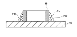
- FIG. 5 is an enlarged schematic view showing a chip part of a comparative example
- FIG. 6 is an enlarged schematic view showing a chip part of an example.
- FL is a residue of a synthetic resin flux containing an acrylic resin
- FL ' is a residue of a general rosin flux
- HD is solder.
- the synthetic resin flux preferably includes at least an acrylic resin. Thereby, the protection performance of a chip component further increases.
- the synthetic resin flux preferably contains at least acrylic. Thereby, the protection performance of a chip component further increases.
- the image sensor and the chip component are sealed in the same space by a base member to which an optical member is fixed.
Landscapes
- Engineering & Computer Science (AREA)
- Multimedia (AREA)
- Signal Processing (AREA)
- Human Computer Interaction (AREA)
- Studio Devices (AREA)
- Lens Barrels (AREA)
Abstract
小型でありながら、撮像素子の撮像面へのフラックス残渣片の付着を抑制でき、耐衝撃性を向上させつつ、高画質な画像を形成できるカメラモジュールの製造方法、カメラモジュール及びかかるカメラモジュールを用いた携帯端末を提供する。半田ペーストHP上にチップ部品18を載置して、リフロー炉RF内に挿入し、半田溶融温度以上に維持する。すると、まず半田ペーストHP内の合成樹脂系フラックスがチップ部品18と配線パターンに展開し、酸化物を洗浄した後に、半田ペーストHP内の粒状半田が溶融し、その後リフロー炉RFから出されることで冷えて固化する。このとき、合成樹脂系フラックスの残渣FLが、固化した半田HDの周囲をコーティングするようになるが、合成樹脂系フラックスの残渣FLは固化しても弾性を失わないので、自身が剥がれ落ちることがなく、また衝撃が付与されたときに半田HDの脱落を保護する機能も有する。加えて、半田付けされたチップ部品18と配線パターンの端子も,合成樹脂系フラックスの残渣FLでコーティングすることで、防湿性も向上する。
Description
本発明は、CCD型イメージセンサあるいはCMOS型イメージセンサ等の撮像素子を用いた小型のカメラモジュールの製造方法、カメラモジュール及びかかるカメラモジュールを用いた携帯端末に関する。
近年、CCD(Charge Coupled Device)型イメージセンサあるいはCMOS(Complementary Metal Oxide Semiconductor)型イメージセンサ等の固体撮像素子を用いたカメラモジュールが搭載された携帯端末の普及の増大に伴い、より高画質の画像が得られるよう、高画素数の撮像素子を使用したカメラモジュールが搭載されたものが市場に供給されるようになってきた。又、携帯端末としては、薄形のスマートフォンなどが主流となりつつあり、これに応じてカメラモジュールの一層の小型化の要求も高まっている。
ところで、カメラモジュールに用いる撮像素子が実装される回路基板には、撮像素子からの信号を処理する小さなチップ部品が、半田ペーストを介して回路基板に実装されている。ここで、半田ペースト内には、酸化物の洗浄用にフラックスが通常混合されている。フラックスは、半田ペーストが加熱された際にいち早く端子表面に回り込み、酸化物を除去することで通電性を高めるという機能がある。
ところで、一般に用いられているロジン系フラックスは、半田加熱後に半田表面を覆って固化し残渣となって残るが、その特性上、ひび割れが生じやすく、衝撃を受けた際にフラックス残渣片が剥離脱落する恐れがある。剥離脱落したフラックス残渣片が、撮像素子の撮像面に落下し付着すると、被写体像上の黒点と認識され、画質の悪化を招くことになる。また、この問題はカメラモジュールが携帯端末等の機器に搭載された後の、使用中の振動、衝撃等により発生する場合が多く、製造工程中で不良品として選別することはできない。一般的にフラックスは、半田付け後はその機能を失うため、洗浄によりチップ部品からフラックスを除去することもできるが、洗浄設備を必要とし、洗浄工程が追加となるなどして、コスト増を招くこととなるので好ましくない。
これに対し特許文献1には、チップ部品を実装するための半田ペーストやフラックス残渣が振動や衝撃等によって剥離し、撮像素子に付着することを防止するために、撮像素子を密閉する空間と、チップ部品及びその周辺領域を収容するチップ部品収納空間とを形成して、両空間を孤立させたカメラモジュールが開示されている。
ここで、特許文献1のカメラモジュールの場合、撮像素子とチップ部品を防塵壁で隔離することにより、チップ部品から剥離した半田ペーストやフラックス残渣が、撮像素子に到達することを防止しているが、撮像素子とチップ部品との間に防塵壁を設けると、その分回路基板を大型化せざるを得ず、このためカメラモジュールが大型化するという問題がある。
本発明は、このような問題点に鑑みてなされたものであり、小型でありながら、撮像素子の撮像面へのフラックス残渣片の付着を抑制でき、耐衝撃性を向上させつつ、高画質な画像を形成できるカメラモジュールの製造方法、カメラモジュール及びかかるカメラモジュールを用いた携帯端末を提供することを目的とする。
本発明によるカメラモジュールの製造方法は、被写体像を形成する撮像レンズと、前記撮像レンズにより形成された被写体像を光電変換する撮像素子と、前記撮像素子及びチップ部品が実装される回路基板と、を有するカメラモジュールの製造方法であって、前記回路基板に前記チップ部品を実装する工程と、前記回路基板に前記撮像素子を実装する工程と、前記回路基板に台座部材及び/又は前記撮像レンズを組み付ける工程を有し、前記回路基板に前記チップ部品を実装する工程において、前記チップ部品を合成樹脂系フラックスを混合した半田ペーストを用いて前記回路基板に接続することを特徴とする。
本発明によるカメラモジュールは、被写体像を形成する撮像レンズと、前記撮像レンズにより形成された被写体像を光電変換する撮像素子と、前記撮像素子及びチップ部品が実装される回路基板と、を有するカメラモジュールにおいて、前記回路基板に実装されるチップ部品は、合成樹脂系フラックスを混合した半田ペーストを用いて、前記回路基板に接続されてなることを特徴とする。
本発明によれば、チップ部品を、合成樹脂系フラックスを混合した半田ペーストを用いて、回路基板に接続することで、合成樹脂系フラックスの残渣が半田を覆って固化した後に、ある程度の弾力性を維持するので、ひび割れが生じにくく、衝撃が付与された場合でもフラックス残渣片が剥離飛散することを抑制でき、これにより同じ回路基板上に実装された撮像素子が汚染されることを抑制できるから、防塵壁等を設ける必要がなくなり、カメラモジュールを小型化できる。又、チップ部品は長さ1mm以下の部品が多いので、半田付けされた部分の面積が小さいことから、強い衝撃を受けると剥がれる恐れがあるが、チップ部品を合成樹脂系フラックスの残渣で覆うことで、回路基板との結合性を高めてチップ部品の脱落を抑制でき、これにより耐衝撃性が向上する。又、チップ部品を合成樹脂系フラックスの残渣で覆うことで、透湿を抑制し、チップ部品の信頼性も高まる。フラックスとは、大気下(大気圧下、酸素存在下)で、電気的接続構造、特に金属同士を接合する場合に用いられるはんだや低融点金属などのろう材と共に用いられる融剤である。フラックスは接合面の酸化物などの異物を除去し、さらに接合部材との界面張力を低減することにより、ろう材の広がり性を向上させ、接合面の金属の酸化を防止することを目的に用いられるものである。合成樹脂系フラックスとしては、例えば千住金属工業株式会社の製品名M705-GRN360-S2、タムラ製作所株式会社の製品名TLF-204-GTS-VR1などを好適に用いることが出来る。
なお、フラックスとしては、樹脂系、有機酸系、無機酸系のものに区分され、更に樹脂系としては、ロジンを主剤とするもの、変性ロジンを主剤とするもの、合成樹脂を主剤とするものがある。本発明は、このうち合成樹脂を主剤とするフラックスを混合した半田ペーストを用いるということである。
本発明による携帯端末は、上述のカメラモジュールと、前記カメラモジュールで得られた被写体像を表示する表示部及び/又は前記カメラモジュールで得られた被写体像を送信する無線通信部と、を有することを特徴とする。
本発明によれば、小型でありながら、撮像素子の撮像面へのフラックス残渣片の付着を抑制でき、耐衝撃性を向上させつつ、高画質な画像を形成できるカメラモジュール、並びにかかるカメラモジュールを用いた携帯端末を提供することができる。
以下、本発明の実施の形態を、図面を参照して説明する。図1は、本実施の形態にかかるカメラモジュール10の断面図である。なお、図1は概略図であり、形状や寸法等は実際と異なるものがある。
図1に示すように、カメラモジュール10は、光電変換部11aを備えた固体撮像素子としてのCMOS型撮像素子11と、この撮像素子11の光電変換部11aに被写体像を形成する撮像レンズ12と、撮像レンズ12を保持する鏡筒13と、IRカットフィルタ及び/又はローパスフィルタで構成された平行平板状の光学フィルタ14と、撮像レンズ12を駆動するアクチュエータ15と、撮像素子11及び回路用のチップ部品18を実装した回路基板16と、撮像レンズ12及びアクチュエータ15を保持する台座部材17とを有する。なお、チップ部品とは、チップ抵抗、チップコンデンサ、チップインダクタ等を指し、例えば、3216サイズ (3.2mm×1.6mm)、2012サイズ (2.0mm×1.2mm)、1608サイズ (1.6mm×0.8mm)、1005サイズ (1.0mm×0.5mm)、0603サイズ (0.6mm×0.3mm)、0402サイズ (0.4mm×0.2mm)等がある。
図1に示すように、撮像素子11は、ウェハ11b上に複数の受光画素(光電変換素子)が2次元的に配置された、撮像面としての光電変換部11aが形成されており、その周囲には信号処理回路(不図示)が形成されている。かかる信号処理回路は、各画素を順次駆動し出力信号を得る駆動回路部と、各出力信号をデジタル信号に変換するA/D変換部と、このデジタル信号を用いて画像信号出力を形成する信号処理部等から構成されている。
また、撮像素子11のウェハ11bにおける受光面側の外縁近傍に形成された複数のパッド(不図示)は、ワイヤ11cにより回路基板16に接続されている。又、回路基板16上において、撮像素子11の周囲には、撮像素子11から出力された信号を処理する配線パターンが形成されており、該配線パターン上にチップ部品18が半田により実装されている。
樹脂により一体成形された台座部材17は、全体的に直方体の筐体状であり、撮像素子11を囲うように設けられた4つの側壁部17aと、その上端に交差する上壁部17bとを有する。上壁部17bの中央には、矩形状の開口17cが形成されており、かかる開口17cを覆うようにして上壁部17bに光学フィルタ14が取り付けられている。すなわち、撮像素子11とチップ部品18は、光学フィルタ14が固着された台座部材17により同じ空間内で封止されている。
撮像素子11は、光電変換部11aからの出力信号をデジタルYUV信号等の画像信号等に変換し、ワイヤ11cから回路基板16の配線パターンを介して、不図示の外部回路(例えば、カメラモジュールを実装した上位装置が有する制御回路)へと送信するようになっている。又、回路基板16の配線パターンからワイヤ11cを介して、外部回路から撮像素子11を駆動するための電力やクロック信号の供給を受けることもできる。ここで、Yは輝度信号、U(=R-Y)は赤と輝度信号との色差信号、V(=B-Y)は青と輝度信号との色差信号である。なお、撮像素子は上記CMOS型のイメージセンサに限定されるものではなく、CCD等の他のものを使用しても良い。
図1において、鏡筒13の内部には、撮像レンズ12が設けられている。アクチュエータ15は、鏡筒13にねじ固定された筒状のキャリヤ15aと、キャリヤ15aに取り付けられ光軸方向に延在するコイル15bと、コイル15bに対向して配置された磁石15cと、磁石15cを支持した筐体状のヨーク15dとからなっている。コイル15bは、不図示の配線を介して外部回路に接続されている。ヨーク15dの下端は、台座部材17の上壁部17b上に接着されている。また、キャリヤ15aは不図示の弾性部材により撮像素子11方向に付勢されている。
次に、カメラモジュール10の製造方法について説明する。図2(a)~(g)は、カメラモジュール10の製造工程を示す図であるが、構成要素を一部簡略化して示している。まず、図2(a)に示すように、配線パターンが表面にプリントされた回路基板16が配置され、更に図2(b)に示すように、回路基板16上の配線パターンに沿って半田ペーストHPを塗布する。半田ペーストHPは、アクリル系樹脂を含む合成樹脂系フラックス内に粒状の半田を混入しており、例えばスクリーン印刷などの手法で塗布される。
その後、図2(c)に示すように、半田ペーストHP上にチップ部品18を載置して、図2(d)に示すように、リフロー炉RF内に挿入し、半田の溶融温度以上に維持する(例えば、一般的な、Sn-3AG-0.5Cuの場合、220℃以上)。すると、まず半田ペーストHP内の合成樹脂系フラックスがチップ部品18と配線パターンに展開し、酸化物を洗浄した後に、半田ペーストHP内の粒状半田が溶融し、その後リフロー炉RFから出されることで冷えて固化する。このとき、合成樹脂系フラックスの残渣FLが、固化した半田HDの周囲をコーティングするようになるが、合成樹脂系フラックスの残渣FLは固化しても弾性を失わないので、自身が剥がれ落ちることがなく、また衝撃が付与されたときに半田HDやチップ部品18の脱落を保護する機能も有する。加えて、半田付けされたチップ部品18と配線パターンの端子も、合成樹脂系フラックスの残渣FLでコーティングでき、防湿性も向上する。
更に、図2(e)に示すように、チップ部品18を実装した回路基板16に、撮像素子11を載置固定して、ワイヤ11cでボンディングにより接続される。その後、図2(f)に示すように、回路基板16に、光学フィルタ14を取り付けた台座部材17を接着し、図2(g)に示すように、台座部材17上に、撮像レンズ12及び鏡筒13を保持したアクチュエータ15を載置し接着剤で固定する。以上で、カメラモジュール10が完成する。なお、図2では、回路基板16に台座部材17を組み付け、台座部材17上に撮像レンズを組み付けるもので説明したが、これに限るものでなく、台座部材17を省略し回路基板16に撮像レンズを組み付けるものであってもよい。
上述したカメラモジュール10の動作について説明する。図3(a)(b)は、カメラモジュール10を携帯端末の一例であるスマートフォン100に装備した状態を示す。また、図4はスマートフォン100の制御ブロック図である。
カメラモジュール10は、例えば、鏡筒13の物体側端面がスマートフォン100の背面(図3(b)参照)に設けられ、スマートフォン100の表面側には液晶表示部が配設されている。
カメラモジュール10は、外部接続端子(図4では矢印)を介して、スマートフォン100の制御部101と接続され、輝度信号や色差信号等の画像信号を制御部101側に出力する。
一方、スマートフォン100は、図4に示すように、各部を統括的に制御すると共に、各処理に応じたプログラムを実行する制御部(CPU)101と、電源等のスイッチ及び番号等をタッチパッドにより指示入力するための入力部60と、所定のデータの他に撮像した映像等を液晶パネルで表示する表示部65(但し、表示部の液晶パネルと入力部のタッチパッドはタッチパネル70が兼用する)と、外部サーバとの間の各種情報通信を実現するための無線通信部80と、スマートフォン100のシステムプログラムや各種処理プログラム及び端末ID等の必要な諸データを記憶している記憶部(ROM)91と、制御部101によって実行される各種処理プログラムやデータ、若しくは処理データ、或いはカメラモジュール10により得られた撮像データ等を一時的に格納する作業領域として用いられる及び一時記憶部(RAM)92とを備えている。
カメラモジュール10は、スマートフォン100の入力部60の操作によって動作させられ、アクチュエータ15により撮像レンズ12を駆動してオートフォーカス動作を行い、レリーズボタン71等を押圧することで、カメラモジュール10を動作させて撮像を行うことができる。カメラモジュール10から入力された画像信号は、上記スマートフォン100の制御系により、記憶部91や一時記憶部92に記憶されたり、或いは表示部65に表示され、さらには、無線通信部80を介して映像情報として外部に送信される。
以下、本発明者の行った試験について説明する。アクリル系樹脂を含む合成樹脂系フラックスを有する半田ペーストを使用して、図2に示す製造工程でカメラモジュールを製作して実施例とするとともに、一般的なロジン系フラックスを有する半田ペーストを使用して、図2に示す製造工程でカメラモジュールを製作して比較例とした。そのうち、画像検査に合格したカメラモジュールを各1,000個準備した。
このカメラモジュールを樹脂トレーに並べ、床面1mの高さから、床に向けて落下させて、衝撃試験を実施した。床面はコンクリートである。更に、試験後、再度画像検査を行い、画像不良をカウントした。そして、分解解析にて、撮像面に付着した成分を特定しフラックスと同定されたものをカウントした。
図5が、比較例のチップ部品を示す拡大模式図であり、図6が、実施例のチップ部品を示す拡大模式図である。図中、FLは、アクリル系樹脂を含む合成樹脂系フラックスの残渣であり、FL’は、一般的なロジン系フラックスの残渣であり、HDが半田である。
試験結果によれば、従来のロジン系フラックスを有する半田ペーストを使用した比較例では、図5に示すように、フラックス残渣に目視で確認できる割れ目CRが生じ、衝撃試験により剥離飛散したフラックス残渣片が撮像素子の撮像面に付着して生じた不良率が2.0%であった。一方、アクリル系樹脂を含む合成樹脂系フラックスを有する半田ペーストを使用した実施例では、図6に示すように、フラックス残渣に目視で確認できる割れ目は生じず、衝撃試験後にもフラックス残渣片の剥離飛散が抑制されるため、不良率が0.3%に低下した。よって、本発明の効果が確認された。
以下、好ましいカメラモジュールの製造方法およびカメラモジュールの態様についてまとめて説明する。
前記合成樹脂系フラックスは、少なくともアクリル系樹脂を含むことが好ましい。これにより、チップ部品の保護性能が更に高まる。
また、前記合成樹脂系フラックスは、少なくともアクリルを含むことが好ましい。これにより、チップ部品の保護性能が更に高まる。
また、前記撮像素子と前記チップ部品は、光学部材が固着された台座部材により同じ空間内で封止されていることが好ましい。
本発明は、明細書に記載の実施形態、実施例に限定されるものではなく、他の実施例・変形例を含むことは、本明細書に記載された実施形態や技術思想から本分野の当業者にとって明らかである。
10 カメラモジュール
11 撮像素子
11a 光電変換部
11b ウェハ
11c ワイヤ
12 撮像レンズ
13 鏡筒
14 光学フィルタ
15 アクチュエータ
15a キャリヤ
15b コイル
15c 磁石
15d ヨーク
16 回路基板
17 台座部材
17a 側壁部
17b 上壁部
17c 開口
18 チップ部品
60 入力部
65 表示部
70 タッチパネル
71 レリーズボタン
80 無線通信部
92 記憶部
100 スマートフォン
101 制御部
11 撮像素子
11a 光電変換部
11b ウェハ
11c ワイヤ
12 撮像レンズ
13 鏡筒
14 光学フィルタ
15 アクチュエータ
15a キャリヤ
15b コイル
15c 磁石
15d ヨーク
16 回路基板
17 台座部材
17a 側壁部
17b 上壁部
17c 開口
18 チップ部品
60 入力部
65 表示部
70 タッチパネル
71 レリーズボタン
80 無線通信部
92 記憶部
100 スマートフォン
101 制御部
Claims (6)
- 被写体像を形成する撮像レンズと、前記撮像レンズにより形成された被写体像を光電変換する撮像素子と、前記撮像素子及びチップ部品が実装される回路基板と、を有するカメラモジュールの製造方法であって、
前記回路基板に前記チップ部品を実装する工程と、
前記回路基板に前記撮像素子を実装する工程と、
前記回路基板に台座部材及び/又は前記撮像レンズを組み付ける工程と、を有し、
前記回路基板に前記チップ部品を実装する工程において、前記チップ部品を合成樹脂系フラックスを混合した半田ペーストを用いて前記回路基板に接続することを特徴とするカメラモジュールの製造方法。 - 前記合成樹脂系フラックスは、少なくともアクリル系樹脂を含むことを特徴とする請求項1に記載のカメラモジュールの製造方法。
- 被写体像を形成する撮像レンズと、前記撮像レンズにより形成された被写体像を光電変換する撮像素子と、前記撮像素子及びチップ部品が実装される回路基板と、を有するカメラモジュールにおいて、
前記回路基板に実装されるチップ部品は、合成樹脂系フラックスを混合した半田ペーストを用いて、前記回路基板に接続されてなることを特徴とするカメラモジュール。 - 前記合成樹脂系フラックスは、少なくともアクリル系樹脂を含むことを特徴とする請求項3に記載のカメラモジュール。
- 前記撮像素子と前記チップ部品は、光学部材が固着された台座部材により同じ空間内で封止されていることを特徴とする請求項3又は4に記載のカメラモジュール。
- 請求項3~5のいずれか一項に記載のカメラモジュールと、前記カメラモジュールで得られた被写体像を表示する表示部及び/又は前記カメラモジュールで得られた被写体像を送信する無線通信部と、を有することを特徴とする携帯端末。
Applications Claiming Priority (2)
| Application Number | Priority Date | Filing Date | Title |
|---|---|---|---|
| JP2013-063925 | 2013-03-26 | ||
| JP2013063925 | 2013-03-26 |
Publications (1)
| Publication Number | Publication Date |
|---|---|
| WO2014156441A1 true WO2014156441A1 (ja) | 2014-10-02 |
Family
ID=51623436
Family Applications (1)
| Application Number | Title | Priority Date | Filing Date |
|---|---|---|---|
| PCT/JP2014/054620 Ceased WO2014156441A1 (ja) | 2013-03-26 | 2014-02-26 | カメラモジュールの製造方法、カメラモジュール及び携帯端末 |
Country Status (1)
| Country | Link |
|---|---|
| WO (1) | WO2014156441A1 (ja) |
Citations (4)
| Publication number | Priority date | Publication date | Assignee | Title |
|---|---|---|---|---|
| JP2002336992A (ja) * | 2001-05-14 | 2002-11-26 | Nec Corp | 回路基板はんだ付用はんだ加工物及び回路基板 |
| JP2003264367A (ja) * | 2002-03-11 | 2003-09-19 | Tamura Kaken Co Ltd | リフローはんだ付用ソルダーペースト組成物及び回路基板 |
| JP2006019837A (ja) * | 2004-06-30 | 2006-01-19 | Sanyo Electric Co Ltd | 回路モジュール |
| JP2012203669A (ja) * | 2011-03-25 | 2012-10-22 | Sony Corp | 端末装置、情報処理装置、物体識別方法、プログラム及び物体識別システム |
-
2014
- 2014-02-26 WO PCT/JP2014/054620 patent/WO2014156441A1/ja not_active Ceased
Patent Citations (4)
| Publication number | Priority date | Publication date | Assignee | Title |
|---|---|---|---|---|
| JP2002336992A (ja) * | 2001-05-14 | 2002-11-26 | Nec Corp | 回路基板はんだ付用はんだ加工物及び回路基板 |
| JP2003264367A (ja) * | 2002-03-11 | 2003-09-19 | Tamura Kaken Co Ltd | リフローはんだ付用ソルダーペースト組成物及び回路基板 |
| JP2006019837A (ja) * | 2004-06-30 | 2006-01-19 | Sanyo Electric Co Ltd | 回路モジュール |
| JP2012203669A (ja) * | 2011-03-25 | 2012-10-22 | Sony Corp | 端末装置、情報処理装置、物体識別方法、プログラム及び物体識別システム |
Similar Documents
| Publication | Publication Date | Title |
|---|---|---|
| JP4724145B2 (ja) | カメラモジュール | |
| EP1081944B1 (en) | Imaging element, imaging device, camera module and camera system | |
| JP5541088B2 (ja) | 撮像素子パッケージ、撮像素子パッケージの製造方法、及び、電子機器 | |
| KR100991185B1 (ko) | 촬상장치 | |
| JP2005101711A (ja) | 固体撮像装置およびその製造方法 | |
| JP2009049499A (ja) | 半導体チップの実装方法及び半導体装置 | |
| JP2008166753A (ja) | 半導体素子パッケージと、その製造および実装方法 | |
| US8917340B2 (en) | Circuit board assembly and camera module using same | |
| US20130016273A1 (en) | Device Having an Optical Module and a Supporting Plate | |
| JP3984256B2 (ja) | カメラ装置のイメージセンサーモジュール及びその組立方法 | |
| JP2013153361A (ja) | カメラモジュール | |
| JP2009025698A (ja) | 撮像装置 | |
| WO2014156441A1 (ja) | カメラモジュールの製造方法、カメラモジュール及び携帯端末 | |
| CN112913023B (zh) | 摄像元件和摄像装置 | |
| JP2014093632A (ja) | カメラモジュールの製造方法、カメラモジュール及び携帯端末 | |
| JPWO2012008268A1 (ja) | 撮像装置及びその製造方法 | |
| JP6504762B2 (ja) | モジュールの製造方法 | |
| KR101004958B1 (ko) | 카메라 모듈 | |
| JP2006287640A (ja) | 固体撮像素子パッケージ、固体撮像素子実装基板、デジタルカメラ及び固体撮像素子パッケージの実装方法 | |
| JP5599294B2 (ja) | 撮像モジュールおよびその製造方法、並びに電子情報機器 | |
| KR100756245B1 (ko) | 카메라 모듈 | |
| JP2014220461A (ja) | 撮像装置およびその製造方法、並びに電子情報機器 | |
| JPWO2010140395A1 (ja) | 撮像装置及び撮像装置の製造方法 | |
| KR20150064572A (ko) | 카메라 제조방법 | |
| KR101111923B1 (ko) | 카메라 모듈 |
Legal Events
| Date | Code | Title | Description |
|---|---|---|---|
| 121 | Ep: the epo has been informed by wipo that ep was designated in this application |
Ref document number: 14775448 Country of ref document: EP Kind code of ref document: A1 |
|
| NENP | Non-entry into the national phase |
Ref country code: DE |
|
| 122 | Ep: pct application non-entry in european phase |
Ref document number: 14775448 Country of ref document: EP Kind code of ref document: A1 |
|
| NENP | Non-entry into the national phase |
Ref country code: JP |