WO2014155864A1 - 電力変換装置 - Google Patents
電力変換装置 Download PDFInfo
- Publication number
- WO2014155864A1 WO2014155864A1 PCT/JP2013/083816 JP2013083816W WO2014155864A1 WO 2014155864 A1 WO2014155864 A1 WO 2014155864A1 JP 2013083816 W JP2013083816 W JP 2013083816W WO 2014155864 A1 WO2014155864 A1 WO 2014155864A1
- Authority
- WO
- WIPO (PCT)
- Prior art keywords
- phase
- wiring
- voltage
- power supply
- state data
- Prior art date
Links
- 238000006243 chemical reaction Methods 0.000 title claims abstract description 13
- 238000001514 detection method Methods 0.000 claims abstract description 40
- 230000001172 regenerating effect Effects 0.000 claims description 8
- 238000000034 method Methods 0.000 abstract description 15
- 230000008929 regeneration Effects 0.000 abstract description 6
- 238000011069 regeneration method Methods 0.000 abstract description 6
- 230000007274 generation of a signal involved in cell-cell signaling Effects 0.000 description 9
- 238000010586 diagram Methods 0.000 description 6
- 230000018199 S phase Effects 0.000 description 5
- 239000003990 capacitor Substances 0.000 description 3
- 230000002159 abnormal effect Effects 0.000 description 2
- 230000004913 activation Effects 0.000 description 1
- 230000007423 decrease Effects 0.000 description 1
- 238000004519 manufacturing process Methods 0.000 description 1
- 230000001360 synchronised effect Effects 0.000 description 1
Images


Classifications
-
- H—ELECTRICITY
- H02—GENERATION; CONVERSION OR DISTRIBUTION OF ELECTRIC POWER
- H02M—APPARATUS FOR CONVERSION BETWEEN AC AND AC, BETWEEN AC AND DC, OR BETWEEN DC AND DC, AND FOR USE WITH MAINS OR SIMILAR POWER SUPPLY SYSTEMS; CONVERSION OF DC OR AC INPUT POWER INTO SURGE OUTPUT POWER; CONTROL OR REGULATION THEREOF
- H02M7/00—Conversion of ac power input into dc power output; Conversion of dc power input into ac power output
- H02M7/42—Conversion of dc power input into ac power output without possibility of reversal
- H02M7/44—Conversion of dc power input into ac power output without possibility of reversal by static converters
- H02M7/48—Conversion of dc power input into ac power output without possibility of reversal by static converters using discharge tubes with control electrode or semiconductor devices with control electrode
-
- H—ELECTRICITY
- H02—GENERATION; CONVERSION OR DISTRIBUTION OF ELECTRIC POWER
- H02M—APPARATUS FOR CONVERSION BETWEEN AC AND AC, BETWEEN AC AND DC, OR BETWEEN DC AND DC, AND FOR USE WITH MAINS OR SIMILAR POWER SUPPLY SYSTEMS; CONVERSION OF DC OR AC INPUT POWER INTO SURGE OUTPUT POWER; CONTROL OR REGULATION THEREOF
- H02M1/00—Details of apparatus for conversion
- H02M1/32—Means for protecting converters other than automatic disconnection
-
- H—ELECTRICITY
- H02—GENERATION; CONVERSION OR DISTRIBUTION OF ELECTRIC POWER
- H02M—APPARATUS FOR CONVERSION BETWEEN AC AND AC, BETWEEN AC AND DC, OR BETWEEN DC AND DC, AND FOR USE WITH MAINS OR SIMILAR POWER SUPPLY SYSTEMS; CONVERSION OF DC OR AC INPUT POWER INTO SURGE OUTPUT POWER; CONTROL OR REGULATION THEREOF
- H02M7/00—Conversion of ac power input into dc power output; Conversion of dc power input into ac power output
- H02M7/02—Conversion of ac power input into dc power output without possibility of reversal
- H02M7/04—Conversion of ac power input into dc power output without possibility of reversal by static converters
- H02M7/12—Conversion of ac power input into dc power output without possibility of reversal by static converters using discharge tubes with control electrode or semiconductor devices with control electrode
- H02M7/21—Conversion of ac power input into dc power output without possibility of reversal by static converters using discharge tubes with control electrode or semiconductor devices with control electrode using devices of a triode or transistor type requiring continuous application of a control signal
- H02M7/217—Conversion of ac power input into dc power output without possibility of reversal by static converters using discharge tubes with control electrode or semiconductor devices with control electrode using devices of a triode or transistor type requiring continuous application of a control signal using semiconductor devices only
- H02M7/219—Conversion of ac power input into dc power output without possibility of reversal by static converters using discharge tubes with control electrode or semiconductor devices with control electrode using devices of a triode or transistor type requiring continuous application of a control signal using semiconductor devices only in a bridge configuration
-
- H—ELECTRICITY
- H02—GENERATION; CONVERSION OR DISTRIBUTION OF ELECTRIC POWER
- H02P—CONTROL OR REGULATION OF ELECTRIC MOTORS, ELECTRIC GENERATORS OR DYNAMO-ELECTRIC CONVERTERS; CONTROLLING TRANSFORMERS, REACTORS OR CHOKE COILS
- H02P29/00—Arrangements for regulating or controlling electric motors, appropriate for both AC and DC motors
- H02P29/02—Providing protection against overload without automatic interruption of supply
- H02P29/024—Detecting a fault condition, e.g. short circuit, locked rotor, open circuit or loss of load
- H02P29/0241—Detecting a fault condition, e.g. short circuit, locked rotor, open circuit or loss of load the fault being an overvoltage
-
- G—PHYSICS
- G01—MEASURING; TESTING
- G01R—MEASURING ELECTRIC VARIABLES; MEASURING MAGNETIC VARIABLES
- G01R29/00—Arrangements for measuring or indicating electric quantities not covered by groups G01R19/00 - G01R27/00
- G01R29/18—Indicating phase sequence; Indicating synchronism
-
- H—ELECTRICITY
- H02—GENERATION; CONVERSION OR DISTRIBUTION OF ELECTRIC POWER
- H02H—EMERGENCY PROTECTIVE CIRCUIT ARRANGEMENTS
- H02H7/00—Emergency protective circuit arrangements specially adapted for specific types of electric machines or apparatus or for sectionalised protection of cable or line systems, and effecting automatic switching in the event of an undesired change from normal working conditions
- H02H7/08—Emergency protective circuit arrangements specially adapted for specific types of electric machines or apparatus or for sectionalised protection of cable or line systems, and effecting automatic switching in the event of an undesired change from normal working conditions for dynamo-electric motors
- H02H7/097—Emergency protective circuit arrangements specially adapted for specific types of electric machines or apparatus or for sectionalised protection of cable or line systems, and effecting automatic switching in the event of an undesired change from normal working conditions for dynamo-electric motors against wrong direction of rotation
-
- H—ELECTRICITY
- H02—GENERATION; CONVERSION OR DISTRIBUTION OF ELECTRIC POWER
- H02P—CONTROL OR REGULATION OF ELECTRIC MOTORS, ELECTRIC GENERATORS OR DYNAMO-ELECTRIC CONVERTERS; CONTROLLING TRANSFORMERS, REACTORS OR CHOKE COILS
- H02P1/00—Arrangements for starting electric motors or dynamo-electric converters
- H02P1/02—Details of starting control
- H02P1/022—Security devices, e.g. correct phase sequencing
Definitions
- the present invention relates to a power conversion device.
- Patent Document 1 can detect miswiring when two wires are misplaced, but cannot detect miswiring when the phase order is correct, such as when three phases are shifted.
- this method detects the input current of the capacitor input and determines the phase. In this method, it is impossible to detect the microcomputer and the detection circuit when the power is turned on. It is necessary to turn on the main circuit.
- the present invention provides a state data detection unit that detects state data (current, voltage) that enters the regenerative converter from the three-phase power supply when the main circuit terminal is switched, and state data that is detected by the state data detection unit.
- a power comprising: a comparison unit that compares a threshold value; and a determination unit that determines a wiring state between the three-phase power source that enters the main circuit and the three-phase power source that enters the phase detection circuit based on the result of comparison by the comparison unit It is a conversion device.
- a power conversion device capable of confirming the correctness of wiring without causing a real machine to perform a regenerative operation by confirming the phase at the time of power-on without providing a new circuit.
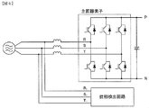
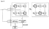
- FIG. 1 is an example of a configuration diagram of the power regeneration device of the present embodiment.
- a connection configuration and operation between a 120-degree energization regenerative converter device 100 (hereinafter, regenerative converter) and a motor control inverter 2 (hereinafter, inverter) will be described.
- the AC side of regenerative converter 100 is connected to a three-phase AC power source 1 (hereinafter referred to as a power source) via an AC reactor 4.
- the power supply 1 may be connected via a reactor, a transformer filter, or the like.
- the main circuit DC unit 107 on the DC side of the main circuit element 200 is connected to the DC unit of the inverter 2 that controls the motor 3.
- the AC side of the inverter 2 is connected to the power source 1.
- the main circuit DC unit 107 holds DC power and is connected to an inverter.
- the voltage of the power supply 1 is converted into an appropriate voltage by a voltage dividing resistor, a phase detection transformer or the like, and then input to the A / D converter to detect the power supply voltage amplitude.
- This power supply voltage amplitude signal is input to the switching control unit 106.
- the current detector 104 detects the current of the main circuit connected to the AC reactor 4. The value is output to the switching control unit 106.
- the inter-PN voltage detection circuit 108 detects the voltage value of the electrolytic capacitor included in the main circuit DC unit 107. The value is output to the switching control unit 106.
- the switching control unit 106 receives a power supply voltage amplitude and a current signal, and a DC voltage signal.
- the regeneration state is determined by comparing the power supply voltage amplitude and the DC voltage, and a GS release signal is output when the motor enters the regeneration state.
- the main circuit element 200 is switched by the six gate pulse signals generated in the gate pulse waveform generation processing 105.
- the phase pulse signal generation circuit 102 receives the voltage of the power supply 1 and outputs a phase pulse signal synchronized with the voltage.
- the phase detection circuit 101 performs PLL processing with the phase pulse signal as an input, and generates a power supply phase signal.
- the gate pulse waveform generation process 105 generates six gate pulse waveforms with the power supply phase signal as an input.
- an input to the phase detection circuit 101 for example, an output of a phase detection transformer or the like may be used instead of the phase pulse signal generation circuit 102.
- the phase reference is arbitrary.
- the gate pulse signal has six main circuit elements (R phase upper side 201, S phase upper side 202, T phase upper side 203, R phase lower side 204, The switching of the S-phase lower side 205 and the T-phase lower side 206 (see FIG. 3) is changed.
- R, S, and T terminals connected to the main circuit element 200 and R1, S1, and T1 terminals connected to the phase pulse signal generation circuit 102 as terminals on the AC side of the regenerative converter.
- the R1, S1, and T1 terminals are directly connected to the power source 1, while the R, S, and T terminals are connected to the power source 1 through a reactor. Normally, this reactor is not housed in the same housing and is placed separately, so the above wiring is performed on the user side.
- the miswiring described at the beginning of this embodiment is that the wiring shown in FIG. 4 is an appropriate wiring (hereinafter referred to as a positive wiring), whereas the R, S, and T terminals connected to the main circuit element 200 and the phase pulse signal. This is a case where the R1, S1, and T1 terminals connected to the generation circuit 102 are wired in different orders. Normal operation in this state is impossible.
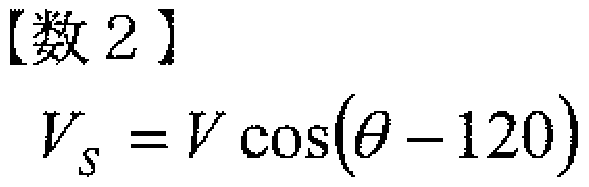
- Equation 1 the voltage of the power supply 1 is as shown in Equation 1, Equation 2, and Equation 3.
- V R represents the phase voltage of the R phase
- V S represents the phase voltage of the S phase
- V T represents the phase voltage of the T phase.
- the DC voltage V dc on the main circuit DC unit 107 side is expressed by Equation 5 when the electrolytic capacitor of the main circuit DC unit 107 is completely charged and becomes a rectified voltage by the diode of the main circuit element 200. .
- the conduction state of the main circuit element is ON for each of the upper arm and the lower arm at an arbitrary phase.
- the phase in which the upper arm is turned on with respect to the phase ⁇ is the phase with the highest voltage, while the lower arm is turned on in the phase with the lowest voltage.
- V1 is a voltage of a phase in which the upper arm is turned on
- V2 is a voltage of a phase in which the lower arm is turned on.
- each gate pulse signal shown in FIG. 3 has a phase ⁇ of 30 degrees, 90 degrees, 150 degrees, 210 degrees, 270 degrees, and 330 degrees.
- ⁇ is the difference between the phase ⁇ and the closest of these angles
- the voltage difference between V1 and V2 that is, the line voltage of the main circuit element that is turned on is expressed by Equation 6.
- Equation 8 the voltage ⁇ V generated in the reactor is expressed by Equation 8.
- Equation 9 Since the state in which the DC voltage Vdc is rectified is obtained by Equation 5, ⁇ V is expressed by Equation 9.
- Equation 10 When the voltage difference ⁇ V is generated in the reactor, the current ⁇ I flowing through the reactor can be obtained by Equation 10.
- ⁇ T is time [s]
- L represents the inductance [H] of the AC reactor 4.
- the voltage ⁇ V generated in the reactor at the time of incorrect wiring is obtained.
- the phase ⁇ is set to 30 degrees.
- the phase voltage of R phase is applied to V1 and the phase voltage of T phase is applied to V2 at the time of positive wiring.
- the S phase voltage is applied.
- the voltage ⁇ V generated here is obtained from Equation 8.
- the power supply voltage is 200 V
- a voltage of approximately 140 V is generated.
- the current ⁇ I flowing at this time is obtained from Equation 10.
- This condition includes that the DC voltage has been rectified, that the CT offset has been completed, and that the PLL has converged for phase detection.
- the rectified voltage can be determined by comparing the power supply voltage amplitude and the DC voltage. If the condition is not satisfied, the check is repeated until the condition is satisfied after waiting for a short time.
- the phase angle ⁇ at which detection is performed is such that the current flowing through the three phases is substantially 0, and therefore the angle at which one of the three phases has a voltage of 0 V is most suitable for detection.
- phase position is good, output a gate pulse signal and stop output after a certain period of time. Since the current value is proportional to the time during which the gate pulse signal is output, the time is determined from the current detection accuracy and the overcurrent level. Thereafter, a current near the peak value is detected. As shown in Table 1, the current is almost zero in the case of the positive wiring, whereas the current flows in the case of incorrect wiring. Therefore, it is possible to determine whether the wiring is correct or not by determining an appropriate threshold value and determining whether or not the threshold value is exceeded.
- the threshold value is determined according to ⁇ V, ⁇ T, and L because the generated current value is expressed by Equation 10. For example, if the L value of the reactor is large, the value of the flowing current decreases, so the threshold value can be lowered. Further, for example, ⁇ V at the time of incorrect wiring is proportional to the voltage of the power supply, so that the threshold value can be determined depending on the power supply voltage.
- the flowing current is calculated by the formula 10, but the detected current value includes errors of various detectors.
- the voltage difference in Table 1 was considered based on the circuit of FIG. 5, but a current to the connected inverter or the like is also generated, and thus deviates from the voltage difference in Table 1 and the value calculated by Equation 10.
- the power supply is unbalanced or includes harmonic distortion, a considerable current flows even with a positive wiring, so it is necessary to increase the threshold value. In these cases, a method of making a determination using a plurality of phases is effective.
- the means of the first embodiment it is possible to determine whether or not the wiring is incorrect.
- an actual wiring pattern is detected, and the switching phase of the main circuit element is changed as will be described later. As a result, operation with actual wiring becomes possible.
- Example 1 a method of changing the switching phase of the main circuit element will be described using the conditions of Example 1 of Example 1.
- the phase in which the main circuit element switches is a phase in which the three-phase AC voltage is not 0.
- the phase with a positive voltage value is the upper side of the main circuit element, and the voltage value is The negative value phase switches the lower element.
- S and T are wired reversely on the AC side of the main circuit element 200, the S-phase lower main circuit to which the T-phase voltage is applied instead of switching the T-phase lower main circuit element. By switching elements, switching according to actual wiring becomes possible.
- a gate pulse signal is output to detect current. If it is confirmed that the wiring is incorrect, the phase of switching of the main circuit element is changed in accordance with (1) of the erroneous wiring pattern in Table 1.
- a gate pulse signal is output to check whether current flows. If the current flows, the wrong wiring pattern (2) is adopted and it is confirmed whether or not a current flows. In this manner, by trying all six types of erroneous wiring patterns in order, it is possible to detect a pattern in which no current flows, that is, an actual wiring pattern.
- the phase pulse signal generation circuit 102 outputs a phase pulse signal switched in accordance with the order of the terminals connected to the main circuit element 200 (in this case, the order is R1, T1, S1). It is also possible to correct.
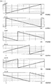
- FIG. 11 is a diagram listing power supply phases for each wiring pattern when the phase to be switched of the main circuit elements is changed when the terminals connected to the phase pulse signal generation circuit 102 are R1, S1, and T1. As can be seen from FIG. 11, the inclination of the power supply phase and the position of the zero point change with each wiring pattern. Therefore, the correction can be made by changing the power supply phase to match each wiring pattern.
- the power phase of the positive wiring (1) may be changed to the power phase of (3).
- (1) since (1) has a normal phase and (3) has a negative phase, it can be corrected by first inverting the power supply phase and then advancing the power supply phase by 120 degrees.
- the actual wiring can be detected without trying all the erroneous wiring patterns as in the second embodiment, the application of extra voltage to the main circuit is reduced, and the standby time until the operation is shortened. effective.
- the estimation method is to find a current value applicable from Table 1 from the current value obtained by the first current detection performed when the power is turned on, and determine a pattern applicable to the current value.
- a function of detecting an incorrect wiring by detecting a voltage will be described.
- a method for determining erroneous wiring from voltage detection will be described below.
- a phase detection circuit 111 and a phase pulse signal generation circuit 112 are provided on the AC side of the main circuit element 200. These perform the same processing as the phase detection circuit 101 and the phase pulse signal generation circuit 102 described in the first embodiment. Therefore, by comparing the power supply phase signals output from the phase detection circuit 101 and the phase detection circuit 111, it is possible to determine that the wiring is the correct wiring if they are the same and the wiring is incorrect if there is a difference.
- a power regeneration device capable of confirming the phase when the power source is activated, detecting all erroneous wirings, and notifying the user of the correct wiring phase regardless of the activation timing of the control power source. Can be provided.
Landscapes
- Engineering & Computer Science (AREA)
- Power Engineering (AREA)
- Inverter Devices (AREA)
- Rectifiers (AREA)
- Testing Of Short-Circuits, Discontinuities, Leakage, Or Incorrect Line Connections (AREA)
Abstract
3相電源用PWMコンバータにおいて、電源入力回路と電源位相検出回路の接続を判定し、正しい配線を使用者に示す方法を提供する。 主回路端子のスイッチング時における三相電源から回生コンバータに入る状態データ(電流、電圧)を検出する状態データ検出部と、前記状態データ検出部にて検出した状態データと予め定めた閾値とを比較する比較部と、前記比較部により比較された結果に基づき、主回路に入る三相電源と位相検出回路へ入る三相電源との配線状態を判断する判断部と、を備える電力変換装置である。
Description
本発明は、電力変換装置に関する。
本技術分野の背景技術として、特開平10-248260号公報がある。この公報には、「二相分の電流検出信号以外の他の一相分の相電圧検出信号の零クロス点を検出して二相分の電流検出信号の大小比較により、接続の正常・異常を判定した。」と記載されている。
特許文献1に開示した方法であると、2線の入れ違いの場合の誤配線は検出できるが、3相ずれた場合など、位相順が合っている場合の誤配線を検出できない。また、コンデンサインプットの入力電流を検出して位相を判定する方法であるが、この方法であると電源投入時マイコン及び検出回路が立ち上がっていないと検出ができないため、別に制御用電源を入れてから主回路部の電源を入れるようにする必要がある。
本願発明は、主回路端子のスイッチング時における三相電源から回生コンバータに入る状態データ(電流、電圧)を検出する状態データ検出部と、前記状態データ検出部にて検出した状態データと予め定めた閾値とを比較する比較部と、前記比較部により比較された結果に基づき、主回路に入る三相電源と位相検出回路へ入る三相電源との配線状態を判断する判断部と、を備える電力変換装置である。
本発明によれば、新たに回路を設けることなく、電源起動時に位相の確認をすることにより、実機に回生動作をさせることなく、配線の正誤を確認できる電力変換装置を提供するものである。
以下、本発明の実施形態を図面を用いて説明する。図を参照して実施例を詳細に説明する。
本実施例では、三相の電流を検出することで配線の間違い(以下、誤配線)を検出する機能を説明する。
図1は、本実施例の電源回生装置の構成図の例である。
図1にて、120度通電回生コンバータ装置100(以下、回生コンバータ)と、モータ制御用インバータ2(以下、インバータ)との接続構成と動作について説明する。図1では、回生コンバータ100の交流側は、交流リアクトル4を介して三相交流電源1(以下、電源)と接続している。ここで、電源1とはリアクトルやトランスフィルタ等を介して接続しても良い。また、主回路素子200の直流側にある主回路直流部107はモータ3を制御するインバータ2の直流部と接続される。また、インバータ2の交流側は、電源1に接続する。
主回路直流部107は、直流電力を保持し、インバータと接続される。
電源電圧検出回路103では、電源1の電圧を分圧抵抗や位相検出トランス等で適切な電圧へ変換した後、A/D変換器に入力して電源電圧振幅を検出する。この電源電圧振幅信号はスイッチング制御部106へ入力する。
電流検出器104では、交流リアクトル4と接続される主回路の電流を検出する。その値をスイッチング制御部106へ出力する。
PN間電圧検出回路108は、主回路直流部107が有する電解コンデンサの電圧値を検出する。その値をスイッチング制御部106へ出力する。
スイッチング制御部106は、電源電圧振幅と電流信号、また、直流電圧信号を入力とする。通常の運転方法では、電源電圧振幅と直流電圧を比較することで回生状態を判断し、モータが回生状態になるとGS解除信号を出力する。このとき、ゲートパルス波形生成処理105で作られた6本のゲートパルス信号にて、主回路素子200がスイッチングする。
位相パルス信号生成回路102は電源1の電圧を入力とし、電圧に同期した位相パルス信号を出力する。位相検出回路101は、位相パルス信号を入力としてPLL処理を行い、電源位相信号を生成する。ゲートパルス波形生成処理105は電源位相信号を入力として6本のゲートパルス波形を生成する。ここで、位相検出回路101への入力は、位相パルス信号生成回路102の代わりに、例えば位相検出用トランス等の出力を利用しても構わない。
この電源位相信号とゲートパルス信号との関係を図2に示す。ここで、位相の基準は任意である。図2のように、ゲートパルス信号は電源位相の角度に合わせて主回路素子200が有する6つの主回路素子(R相上側201、S相上側202、T相上側203、R相下側204、S相下側205、T相下側206(図3参照))のスイッチングを変更する。
回生コンバータの交流側の端子として、主回路素子200へ接続されるR、S、T端子と位相パルス信号生成回路102へ接続されるR1、S1、T1端子とがある。R1、S1、T1端子は電源1に直接接続するのに対し、R、S、T端子はリアクトルを介して電源1に接続する。通常このリアクトルは同一の筐体内に収納せず別置となるので、上記の配線はユーザ側で行われる。
本実施例の冒頭で述べた誤配線とは、図4が適切な配線(以下、正配線)であることに対し、主回路素子200へ接続されるR、S、T端子と、位相パルス信号生成回路102へ接続されるR1、S1、T1端子の順番が異なって配線された場合のことである。この状態での正常な運転は不可能となる。
以下に、誤配線時の判断に必要となる計算式を説明する。
図2の電源位相を使うと、電源1の電圧は数1、数2、数3のようになる。
図2の電源位相を使うと、電源1の電圧は数1、数2、数3のようになる。


VRはR相の相電圧、VSはS相の相電圧、VTはT相の相電圧を表す。Vacを線間電圧の実効値とすると、数4となる。

また、主回路直流部107側の直流電圧Vdcは、主回路直流部107が有する電解コンデンサに充電が完了され、主回路素子200のダイオードによる整流電圧となった場合、数5で表される。

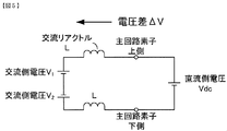
ここで、正配線時に図3に示すゲートパルス信号にて主回路素子を駆動したときにリアクトルにかかる電圧を考える。図3からわかるように、主回路素子の導通状態は、任意の位相で上アームと下アームのそれぞれ一つずつがONとなっている。位相θに対し上アームがONする相は電圧が最も高い相で、一方、下アームがONするのは電圧が最も低い相となっている。ONしている主回路素子の回路のみを取り出すと、図5のようになる。この時、V1は上アームがONする相の電圧で、V2は下アームがONする相の電圧となる。
図3に示される各ゲートパルス信号の中心位置は、位相θが30度、90度、150度、210度、270度、330度となる。位相θとこれらの角度のうち最も近い角度との差をαとすると、V1とV2の電圧差、即ち、ONした主回路素子の線間電圧は数6で表される。

ここで数4を代入すると、数7が求められる。
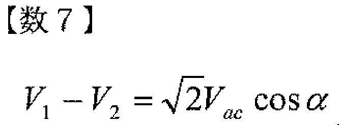
図5の回路から、リアクトルに発生する電圧ΔVは数8となる。

直流電圧Vdcが整流した状態は数5で求められることより、ΔVは数9と表される。

リアクトルに電圧差ΔVが発生した場合、リアクトルに流れる電流ΔIは、数10で求めることができる。このとき、ΔTは時間[s]とし、Lは交流リアクトル4のインダクタンス[H]を表すこととする。

ここで、誤配線時にリアクトルに発生する電圧ΔVを求める。例1として、位相パルス信号生成回路102に接続される端子R1、S1、T1に対し、図6のように主回路素子200側を順にR、T、Sと誤った配線をした場合で考える。このとき、位相θを30度とする。図5の回路で考えると、正配線時にはV1にはR相の相電圧、V2にはT相の相電圧がかかるが、ここではS相とT相の逆相で考えているため、V2にはS相の相電圧がかかる。ここで発生する電圧ΔVは数8から求められ、電源電圧が200Vの場合、およそ140Vの電圧が発生する。このときに流れる電流ΔIは数10より求められる。
任意の配線パターンで接続された場合に発生する電圧を、各ゲートパルス信号の中心点、即ち、α=0の角度で考えると、表1のとおりである。
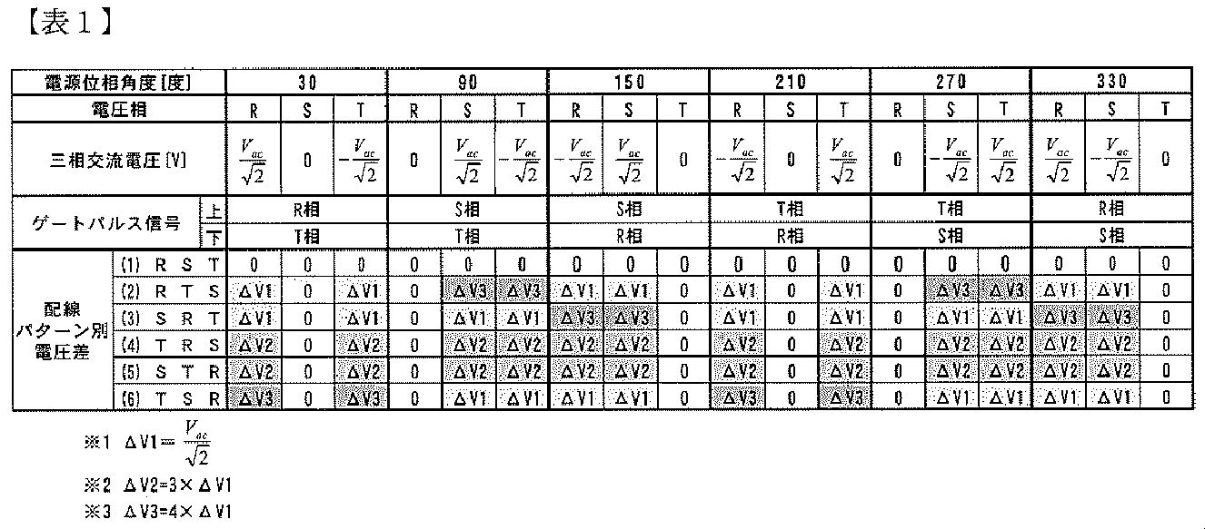
表1より、誤配線時にはどの配線パターンでも任意の位相で電圧差が発生することがわかる。この時、電圧の大小関係は、ΔV1<ΔV2<ΔV3となる。
一方で、正配線時の場合には表中のどの位相であってもリアクトルに電圧差は発生しない。よって、図3のゲートパルスのα=0にて主回路素子を駆動すれば、流れる電流がほぼ零かどうかで正配線かどうかを判断することが可能となる。
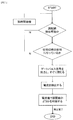
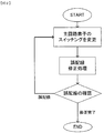
以下に、具体的な誤配線の検出方法を図7のフローチャートを用いて説明する。
まず、誤配線の検出が可能となる条件を満たしているかを判断する。この条件には、直流電圧が整流されていること、CTオフセットが終了していること、また位相検出のためにPLLが収束していること等が挙げられる。整流電圧の判定は電源電圧振幅と直流電圧を比較することで行うことができる。条件を満たしていなければ、短時間の待機後、条件を満たすまで確認を繰り返す。
まず、誤配線の検出が可能となる条件を満たしているかを判断する。この条件には、直流電圧が整流されていること、CTオフセットが終了していること、また位相検出のためにPLLが収束していること等が挙げられる。整流電圧の判定は電源電圧振幅と直流電圧を比較することで行うことができる。条件を満たしていなければ、短時間の待機後、条件を満たすまで確認を繰り返す。
次に、ゲートパルス信号出力に適した位相まで待機する。適していなければ、短時間の待機を行い最初の条件から確認をし直す。検出を行う位相角度θは、三相を流れる電流がほぼ0となるため、三相のうちいずれか一相の電圧が0Vになる角度が最も検出に適する。この角度は30度、90度、150度、210度、270度、330度の6カ所となる。そのため、角度差αができる限り小さい値の位相で検出を行うことを推奨する。しかしながら、正確に上記の6カ所の位相で検出を行えるとは限らないため、閾値を調整することによってある程度ずれた位相でゲートを開くことも可能である。
位相の位置が良ければ、ゲートパルス信号を出力し、一定時間経過後出力を停止する。このゲートパルス信号を出力している時間に電流値が比例するので、電流検出精度や過電流レベルから時間を決定する。その後ピーク値付近の電流を検出する。表1に示す通り、正配線の場合は電流がほぼ零となるのに対し、誤配線時は電流が流れる。よって、適当な閾値を定めてその閾値以上かどうかで配線の正誤が判定可能となる。
閾値の決め方については、発生する電流値が数10で表されるので、ΔV、ΔT、Lに応じて決定する。例えば、リアクトルのL値が大きければ流れる電流値が下がるので閾値は下げることが可能となる。また、例えば誤配線時のΔVは電源の電圧に比例するので、電源電圧に依存して閾値を決定することも可能である。
流れる電流は数10で計算されるが、検出した電流値は各種の検出器の誤差を含む。また、表1の電圧差は図5の回路を基に考えたが、接続されたインバータ等への電流も発生するので、表1の電圧差と数10で計算される値からずれる。さらに電源が不平衡であったり、高調波歪みを含んだりする場合、正配線であっても相当の電流が流れるため、閾値を大きくとる必要がある。これらの場合、複数の位相を使って判断を行う等の方法が有効である。
上記で述べた方法を用いれば、ゲートパルス信号を出力する時間を調整することにより、電流を安全なレベルに制限した上で誤配線を検出することができる。そのため、異常な動作やスイッチングする主回路素子の破損を防止することができる。
また、運転の前に本誤配線検出を行うことで、運転開始時よりも安全に警告を出すことが可能である。
本実施例では、誤配線と判断した場合に、誤配線の状態のままで運転する機能について説明する。
実施例1の手段を使えば誤配線かどうかの判断が可能となるが、本実施例ではそれに加えて、実配線パターンを検出し、後述のように、主回路素子のスイッチングする相を変更することで、実配線のままでの運転が可能となる。
まず、実施例1の例1の条件を使い、主回路素子のスイッチングする相を変更する方法を説明する。表1に示す位相では、主回路素子がスイッチングする相は三相交流電圧が0でない相であり、図8のように、電圧値が正の値の相は主回路素子の上側、電圧値が負の値の相は下側の素子をスイッチングするようになっている。例1では主回路素子200の交流側にSとTを逆に配線しているため、T相下側の主回路素子をスイッチングする代わりに、T相の電圧がかかるS相下側の主回路素子をスイッチングすることで、実際の配線に合わせたスイッチングが可能となる。
次に、実配線パターンの検出方法を説明する。ここで、実施例1で示した誤配線検出方法を用いる。ある誤配線パターンで配線を行っていると仮定し、図9のフローチャートを用いて説明する。初めにゲートパルス信号を出力して電流の検出を行う。ここで誤配線であると確認できた場合、表1にある誤配線パターンの(1)に合わせて主回路素子のスイッチングする相を変更する。ここでまたゲートパルス信号を出力し、電流が流れるかどうかを確認する。流れた場合、誤配線パターンの(2)を採用し、また電流が流れるかどうかを確認する。このように、全6種類の誤配線パターンを順番に試すことで、電流が流れないパターン即ち実配線パターンを検出することが可能となる。
また、例えば図10のように位相パルス信号生成回路102へ接続される端子R1、S1、T1に対し、主回路素子200へ接続される端子の順番をR、T、Sとした場合を考える。このとき、位相パルス信号生成回路102において、主回路素子200へ接続された端子の順番に合わせて入れ替えた位相パルス信号(この場合の順番はR1、T1、S1)を出力することで、誤配線を修正することも可能である。
さらに、電源位相をずらすことで修正することも可能である。図11は位相パルス信号生成回路102へ接続される端子がR1、S1、T1とした場合に、主回路素子のスイッチングする相を変更した際の電源位相を各配線パターン別に列挙した図である。図11からわかるように、各配線パターンで電源位相の傾きや0点の位置は変化する。そのため、各配線パターンに合わせた電源位相に変更することで、修正が可能となる。
以下に、電源位相を修正する具体例を述べる。図11より、(3)の誤配線パターンで接続された場合を例にとると、正配線の電源位相となる(1)を(3)の電源位相になるように変更すればよい。方法として、(1)は順相に対し(3)は逆相であるため、まず電源位相を反転させ、その後電源位相を120度進めることで、修正が可能である。
本実施例では、誤配線と判断した場合に、実配線パターンを推測する機能について説明する。
本実施例では、実施例2のように全ての誤配線パターンを試すことなく、実配線の検出が可能となり、主回路への余分な電圧印加を減らし、かつ、運転までの待機時間を短くする効果がある。
推測を行う方法は、電源投入時に行う初回の電流検出で得られた電流値より、表1の中から当てはまる電流値を見つけ出し、その電流値に当てはまるパターンを決定すればよい。
また、上記で推測したパターンに合わせて実施例2の方法で主回路素子のスイッチングをすると電流は流れない。この方法にて上記の推測が正しいかどうかを簡単に確認することが可能である。
本実施例では、電圧を検出することで誤配線を検出する機能を説明する。
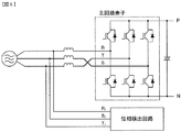
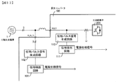
電圧検出から誤配線を判断する方法を以下に説明する。まず、図12のように、主回路素子200の交流側に位相検出回路111と位相パルス信号生成回路112を設ける。これらは、実施例1で説明した位相検出回路101、位相パルス信号生成回路102と同じ処理を行う。よって、位相検出回路101と位相検出回路111が出力する電源位相信号を比較することで、同じであれば正配線、相違があれば誤配線であるという判断が可能となる。
電圧検出から誤配線を判断する方法を以下に説明する。まず、図12のように、主回路素子200の交流側に位相検出回路111と位相パルス信号生成回路112を設ける。これらは、実施例1で説明した位相検出回路101、位相パルス信号生成回路102と同じ処理を行う。よって、位相検出回路101と位相検出回路111が出力する電源位相信号を比較することで、同じであれば正配線、相違があれば誤配線であるという判断が可能となる。
以上説明したとおり、本願発明によって、制御用電源の起動タイミングに係わらず、電源起動時に位相の確認をし、全誤配線について検出し、正しい配線位相を使用者に知らせることのできる電源回生装置を提供することができる。
Claims (5)
- 主回路端子のスイッチング時における三相電源から回生コンバータに入る状態データを検出する状態データ検出部と、
前記状態データ検出部にて検出した状態データと予め定めた閾値とを比較する比較部と、
前記比較部により比較された結果に基づき、主回路に入る三相電源と位相検出回路へ入る三相電源との配線状態を判断する判断部と、
を備える電力変換装置。 - 請求項1記載の電力変換装置であって、
前記状態データ検出部にて検出する状態データは電流値または電圧値のいずれかであることを特徴とする電力変換装置。 - 請求項1に記載の電力変換装置であって、
前記判断部にて誤配線状態であると判断された場合に、警告を表示する表示部を備えることを特徴とする電力変換装置。 - 請求項1に記載の電力変換装置であって、
前記比較部で用いる該予め定めた閾値は0であることを特徴とする電力変換装置。 - 請求項1に記載の電力変換装置であって、
前記判断部にて誤配線状態であると判断された場合に、前記回生コンバータと前記位相検出回路との接続状態を変更することを特徴とする電力変換装置。
Priority Applications (2)
| Application Number | Priority Date | Filing Date | Title |
|---|---|---|---|
| CN201380075161.0A CN105075084B (zh) | 2013-03-29 | 2013-12-18 | 电力转换装置 |
| EP13880091.7A EP2980978A4 (en) | 2013-03-29 | 2013-12-18 | Electric power conversion device |
Applications Claiming Priority (2)
| Application Number | Priority Date | Filing Date | Title |
|---|---|---|---|
| JP2013070975A JP6037913B2 (ja) | 2013-03-29 | 2013-03-29 | 電力変換装置 |
| JP2013-070975 | 2013-03-29 |
Publications (1)
| Publication Number | Publication Date |
|---|---|
| WO2014155864A1 true WO2014155864A1 (ja) | 2014-10-02 |
Family
ID=51622897
Family Applications (1)
| Application Number | Title | Priority Date | Filing Date |
|---|---|---|---|
| PCT/JP2013/083816 WO2014155864A1 (ja) | 2013-03-29 | 2013-12-18 | 電力変換装置 |
Country Status (4)
| Country | Link |
|---|---|
| EP (1) | EP2980978A4 (ja) |
| JP (1) | JP6037913B2 (ja) |
| CN (1) | CN105075084B (ja) |
| WO (1) | WO2014155864A1 (ja) |
Cited By (1)
| Publication number | Priority date | Publication date | Assignee | Title |
|---|---|---|---|---|
| CN106716811A (zh) * | 2014-10-17 | 2017-05-24 | 三菱重工业株式会社 | 整流电路的电流推定电路、ac‑dc转换器、电力控制装置、电流推定电路、电流推定方法及程序 |
Families Citing this family (2)
| Publication number | Priority date | Publication date | Assignee | Title |
|---|---|---|---|---|
| WO2021177193A1 (ja) * | 2020-03-02 | 2021-09-10 | 株式会社日立産機システム | 電力変換装置 |
| CN116325470A (zh) * | 2020-10-26 | 2023-06-23 | 发那科株式会社 | 具有配线状态检测部的转换器以及电动机驱动装置 |
Citations (4)
| Publication number | Priority date | Publication date | Assignee | Title |
|---|---|---|---|---|
| JPH08251927A (ja) * | 1995-03-13 | 1996-09-27 | Hitachi Ltd | 誤配線検出装置 |
| JPH10248260A (ja) | 1997-03-05 | 1998-09-14 | Meidensha Corp | 主回路接続判定方法 |
| JP2012016206A (ja) * | 2010-07-02 | 2012-01-19 | Hitachi Ltd | 電力変換装置のゲートパルス誤配線検出方法 |
| JP2012249494A (ja) * | 2011-05-31 | 2012-12-13 | Hitachi Industrial Equipment Systems Co Ltd | 電源回生装置 |
Family Cites Families (9)
| Publication number | Priority date | Publication date | Assignee | Title |
|---|---|---|---|---|
| AT398867B (de) * | 1989-12-12 | 1995-02-27 | Siemens Ag Oesterreich | Schaltungsanordnung zur bestimmung der phasenlage von unterschiedlichen versorgungsspannungen, insbesondere für netzgeführte stromrichter |
| JP2797882B2 (ja) * | 1993-03-12 | 1998-09-17 | 三菱電機株式会社 | サーボモータの制御装置 |
| JPH08289466A (ja) * | 1995-04-17 | 1996-11-01 | Sanyo Electric Co Ltd | 電源誤配線検知装置 |
| JP3625901B2 (ja) * | 1995-06-30 | 2005-03-02 | 三菱電機株式会社 | サーボ制御システムの自動適正化方法および装置 |
| US6066932A (en) * | 1998-07-06 | 2000-05-23 | Fetzer; Fred | Motor reversal protection apparatus |
| KR20040034906A (ko) * | 2002-10-17 | 2004-04-29 | 엘지전자 주식회사 | 멀티 공조기의 역상/결상 감지방법 |
| CN2674463Y (zh) * | 2004-01-16 | 2005-01-26 | 广东新的科技集团有限公司 | 一种相序检测控制系统 |
| JP5331523B2 (ja) * | 2009-03-12 | 2013-10-30 | 山洋電気株式会社 | 誤配線検出機能を備えた三相同期電動機の制御装置 |
| CN102739085B (zh) * | 2012-06-20 | 2014-07-02 | 陕西煤业化工技术研究院有限责任公司 | 逆变器锁相和相序识别的方法 |
-
2013
- 2013-03-29 JP JP2013070975A patent/JP6037913B2/ja active Active
- 2013-12-18 EP EP13880091.7A patent/EP2980978A4/en not_active Ceased
- 2013-12-18 WO PCT/JP2013/083816 patent/WO2014155864A1/ja active Application Filing
- 2013-12-18 CN CN201380075161.0A patent/CN105075084B/zh active Active
Patent Citations (4)
| Publication number | Priority date | Publication date | Assignee | Title |
|---|---|---|---|---|
| JPH08251927A (ja) * | 1995-03-13 | 1996-09-27 | Hitachi Ltd | 誤配線検出装置 |
| JPH10248260A (ja) | 1997-03-05 | 1998-09-14 | Meidensha Corp | 主回路接続判定方法 |
| JP2012016206A (ja) * | 2010-07-02 | 2012-01-19 | Hitachi Ltd | 電力変換装置のゲートパルス誤配線検出方法 |
| JP2012249494A (ja) * | 2011-05-31 | 2012-12-13 | Hitachi Industrial Equipment Systems Co Ltd | 電源回生装置 |
Non-Patent Citations (1)
| Title |
|---|
| See also references of EP2980978A4 * |
Cited By (2)
| Publication number | Priority date | Publication date | Assignee | Title |
|---|---|---|---|---|
| CN106716811A (zh) * | 2014-10-17 | 2017-05-24 | 三菱重工业株式会社 | 整流电路的电流推定电路、ac‑dc转换器、电力控制装置、电流推定电路、电流推定方法及程序 |
| CN106716811B (zh) * | 2014-10-17 | 2020-07-28 | 三菱重工业株式会社 | 整流电路的电流推定电路、ac-dc转换器、电力控制装置、电流推定方法及记录介质 |
Also Published As
| Publication number | Publication date |
|---|---|
| JP2014195375A (ja) | 2014-10-09 |
| EP2980978A1 (en) | 2016-02-03 |
| JP6037913B2 (ja) | 2016-12-07 |
| CN105075084A (zh) | 2015-11-18 |
| EP2980978A4 (en) | 2017-02-15 |
| CN105075084B (zh) | 2017-10-13 |
Similar Documents
| Publication | Publication Date | Title |
|---|---|---|
| JP5689497B2 (ja) | Dcリンク部異常検出機能を備えたモータ駆動装置 | |
| US10333311B2 (en) | Electric motor control device | |
| AU2016324266B2 (en) | Inverter substrate, method for determining connection sequence, and method for determining open phase | |
| JP2016201922A (ja) | 交流電動機駆動システム及び交流電動機配線異常検出装置 | |
| JP3960350B1 (ja) | 地絡検出方法 | |
| US9941815B2 (en) | Power conversion apparatus with overcurrent simulating circuit | |
| JP6686685B2 (ja) | 電力変換装置 | |
| JP6037913B2 (ja) | 電力変換装置 | |
| KR102620030B1 (ko) | 전원 장치 및 교류 전원의 이상 검출 방법 | |
| CN107960144B (zh) | 逆变器装置 | |
| JP2008253008A (ja) | 電力変換装置および電源誤接続判定方法 | |
| JP6230677B1 (ja) | 回転電機の制御装置および制御方法 | |
| KR101702200B1 (ko) | 정류 장치 및 정류 시스템 | |
| JP5369818B2 (ja) | インバータ装置の故障検出方法 | |
| KR101195157B1 (ko) | 결선이상 검출기능이 구비된 모터제어 인버터 | |
| JP2021044930A (ja) | 電力変換装置、および電力変換装置の制御方法 | |
| JP4697579B2 (ja) | 電力変換装置と欠相検出方法 | |
| JP6012453B2 (ja) | Pwmコンバータ装置およびエレベータ装置 | |
| JP2011151974A (ja) | 電力変換装置 | |
| JP2014082860A (ja) | モータ装置 | |
| JP2007325416A (ja) | 整流回路の制御装置 |
Legal Events
| Date | Code | Title | Description |
|---|---|---|---|
| WWE | Wipo information: entry into national phase |
Ref document number: 201380075161.0 Country of ref document: CN |
|
| 121 | Ep: the epo has been informed by wipo that ep was designated in this application |
Ref document number: 13880091 Country of ref document: EP Kind code of ref document: A1 |
|
| WWE | Wipo information: entry into national phase |
Ref document number: 2013880091 Country of ref document: EP |
|
| NENP | Non-entry into the national phase |
Ref country code: DE |