WO2014142153A1 - Solder alloy and joint thereof - Google Patents
Solder alloy and joint thereof Download PDFInfo
- Publication number
- WO2014142153A1 WO2014142153A1 PCT/JP2014/056440 JP2014056440W WO2014142153A1 WO 2014142153 A1 WO2014142153 A1 WO 2014142153A1 JP 2014056440 W JP2014056440 W JP 2014056440W WO 2014142153 A1 WO2014142153 A1 WO 2014142153A1
- Authority
- WO
- WIPO (PCT)
- Prior art keywords
- solder
- joint
- alloy
- intermetallic compound
- weight
- Prior art date
Links
Images


Classifications
-
- C—CHEMISTRY; METALLURGY
- C22—METALLURGY; FERROUS OR NON-FERROUS ALLOYS; TREATMENT OF ALLOYS OR NON-FERROUS METALS
- C22C—ALLOYS
- C22C13/00—Alloys based on tin
-
- B—PERFORMING OPERATIONS; TRANSPORTING
- B23—MACHINE TOOLS; METAL-WORKING NOT OTHERWISE PROVIDED FOR
- B23K—SOLDERING OR UNSOLDERING; WELDING; CLADDING OR PLATING BY SOLDERING OR WELDING; CUTTING BY APPLYING HEAT LOCALLY, e.g. FLAME CUTTING; WORKING BY LASER BEAM
- B23K1/00—Soldering, e.g. brazing, or unsoldering
- B23K1/0006—Exothermic brazing
-
- B—PERFORMING OPERATIONS; TRANSPORTING
- B23—MACHINE TOOLS; METAL-WORKING NOT OTHERWISE PROVIDED FOR
- B23K—SOLDERING OR UNSOLDERING; WELDING; CLADDING OR PLATING BY SOLDERING OR WELDING; CUTTING BY APPLYING HEAT LOCALLY, e.g. FLAME CUTTING; WORKING BY LASER BEAM
- B23K1/00—Soldering, e.g. brazing, or unsoldering
- B23K1/0008—Soldering, e.g. brazing, or unsoldering specially adapted for particular articles or work
- B23K1/0016—Brazing of electronic components
-
- B—PERFORMING OPERATIONS; TRANSPORTING
- B23—MACHINE TOOLS; METAL-WORKING NOT OTHERWISE PROVIDED FOR
- B23K—SOLDERING OR UNSOLDERING; WELDING; CLADDING OR PLATING BY SOLDERING OR WELDING; CUTTING BY APPLYING HEAT LOCALLY, e.g. FLAME CUTTING; WORKING BY LASER BEAM
- B23K1/00—Soldering, e.g. brazing, or unsoldering
- B23K1/19—Soldering, e.g. brazing, or unsoldering taking account of the properties of the materials to be soldered
-
- B—PERFORMING OPERATIONS; TRANSPORTING
- B23—MACHINE TOOLS; METAL-WORKING NOT OTHERWISE PROVIDED FOR
- B23K—SOLDERING OR UNSOLDERING; WELDING; CLADDING OR PLATING BY SOLDERING OR WELDING; CUTTING BY APPLYING HEAT LOCALLY, e.g. FLAME CUTTING; WORKING BY LASER BEAM
- B23K35/00—Rods, electrodes, materials, or media, for use in soldering, welding, or cutting
- B23K35/001—Interlayers, transition pieces for metallurgical bonding of workpieces
- B23K35/007—Interlayers, transition pieces for metallurgical bonding of workpieces at least one of the workpieces being of copper or another noble metal
-
- B—PERFORMING OPERATIONS; TRANSPORTING
- B23—MACHINE TOOLS; METAL-WORKING NOT OTHERWISE PROVIDED FOR
- B23K—SOLDERING OR UNSOLDERING; WELDING; CLADDING OR PLATING BY SOLDERING OR WELDING; CUTTING BY APPLYING HEAT LOCALLY, e.g. FLAME CUTTING; WORKING BY LASER BEAM
- B23K35/00—Rods, electrodes, materials, or media, for use in soldering, welding, or cutting
- B23K35/22—Rods, electrodes, materials, or media, for use in soldering, welding, or cutting characterised by the composition or nature of the material
- B23K35/24—Selection of soldering or welding materials proper
- B23K35/28—Selection of soldering or welding materials proper with the principal constituent melting at less than 950 degrees C
- B23K35/282—Zn as the principal constituent
-
- B—PERFORMING OPERATIONS; TRANSPORTING
- B23—MACHINE TOOLS; METAL-WORKING NOT OTHERWISE PROVIDED FOR
- B23K—SOLDERING OR UNSOLDERING; WELDING; CLADDING OR PLATING BY SOLDERING OR WELDING; CUTTING BY APPLYING HEAT LOCALLY, e.g. FLAME CUTTING; WORKING BY LASER BEAM
- B23K35/00—Rods, electrodes, materials, or media, for use in soldering, welding, or cutting
- B23K35/22—Rods, electrodes, materials, or media, for use in soldering, welding, or cutting characterised by the composition or nature of the material
- B23K35/24—Selection of soldering or welding materials proper
- B23K35/30—Selection of soldering or welding materials proper with the principal constituent melting at less than 1550 degrees C
- B23K35/3006—Ag as the principal constituent
-
- B—PERFORMING OPERATIONS; TRANSPORTING
- B23—MACHINE TOOLS; METAL-WORKING NOT OTHERWISE PROVIDED FOR
- B23K—SOLDERING OR UNSOLDERING; WELDING; CLADDING OR PLATING BY SOLDERING OR WELDING; CUTTING BY APPLYING HEAT LOCALLY, e.g. FLAME CUTTING; WORKING BY LASER BEAM
- B23K2101/00—Articles made by soldering, welding or cutting
- B23K2101/36—Electric or electronic devices
-
- B—PERFORMING OPERATIONS; TRANSPORTING
- B23—MACHINE TOOLS; METAL-WORKING NOT OTHERWISE PROVIDED FOR
- B23K—SOLDERING OR UNSOLDERING; WELDING; CLADDING OR PLATING BY SOLDERING OR WELDING; CUTTING BY APPLYING HEAT LOCALLY, e.g. FLAME CUTTING; WORKING BY LASER BEAM
- B23K2103/00—Materials to be soldered, welded or cut
- B23K2103/08—Non-ferrous metals or alloys
- B23K2103/12—Copper or alloys thereof
-
- B—PERFORMING OPERATIONS; TRANSPORTING
- B23—MACHINE TOOLS; METAL-WORKING NOT OTHERWISE PROVIDED FOR
- B23K—SOLDERING OR UNSOLDERING; WELDING; CLADDING OR PLATING BY SOLDERING OR WELDING; CUTTING BY APPLYING HEAT LOCALLY, e.g. FLAME CUTTING; WORKING BY LASER BEAM
- B23K2103/00—Materials to be soldered, welded or cut
- B23K2103/18—Dissimilar materials
Definitions
- the present invention relates to an improved technique capable of obtaining a stable and strong joint interface when joining a Cu alloy terminal to an Ag electrode in Sn—Zn solder, and in particular, to a Cu alloy on an Ag electrode fixed on a glass surface.
- the present invention relates to a solder alloy suitable for a solder for joining terminal components, and a joined product thereof.
- solder alloys that do not contain Pb have become mainstream in consideration of environmental considerations, and Sn—Zn based solder alloys are known as one type.
- solder alloy is to join metal and metal at a relatively low melting point, but when the metal to be joined is not included in the solder alloy, the joining metal is soldering work.
- a so-called erosion phenomenon occurs in which the molten solder elutes.
- the bonding target is Cu
- copper is eroded
- Ag is Ag
- silver erosion occurs.
- the eluted metal and a part of the solder alloy composition form an intermetallic compound at the bonding interface, and solidify. And stick. In soldering, it is inevitable that an intermetallic compound is generated between a metal eluted from an object to be soldered and a metal contained in the solder alloy.
- the generated intermetallic compound has a relatively large particle size when solidified, it causes deterioration over time at the bonding interface. That is, in an intermetallic compound formed of multiple types of metals, Kirkendall voids appear due to the difference in the diffusion rate of metal atoms, and this develops into cracks over time due to external factors such as external stress and heat cycle. There is a risk that the joint interface may eventually break.
- the particle size of the intermetallic compound is large, the difference in the diffusion rate of the metal atoms is particularly affected, and the probability of occurrence of Kirkendall void is considered to increase. Therefore, even when Sn—Zn-based solder is selected, it is preferable that the solidification particle size of the intermetallic compound at the joint interface is as small as possible depending on the joint.
- Patent Document 1 is a composition containing a small amount of an additive component with respect to the Sn—Zn system, and Mn is exemplified as the additive component. Further, it is described that these compositions are intended to improve the stability of Sn—Zn solder when it is prepared into a solder paste, and to suppress the temporal change of the solder after joining.
- this known technique does not specify the composition of the joint, and does not consider that an intermetallic compound is generated between the solder composition and the composition of the joint.
- Patent Document 2 discloses a technique in which Mn is added as a kind of deoxidizer, focusing on the fact that manganese reacts strongly with oxygen with Sn—Zn as the main component. And it is described that the high solder joint characteristic with respect to the metal electrode on glass was discovered by this.
- Patent Document 3 describes a solder alloy composed of 0.01 to 10% by weight of Zn, 0.1% by weight or less of Mn, and the balance being Sn.
- conventional metal parts such as Cu and Ni, which are the materials for solder joints of printed circuit boards and electronic components, high solder joint characteristics for metal electrodes on glass are disclosed. It assumes solder jointability with Al.
- Patent Document 4 discloses that an Sn—Zn alloy containing 0.001 to 0.9% by weight of Mn is used as a solder alloy. This known technique does not take into consideration an intermetallic compound generated between the solder composition and the composition of the joint as in the other known techniques.
- the present invention is based on the premise that a joint is joined to an Ag joint using a Sn—Zn-based solder composition, and an intermetallic compound called AgZn is generated between Zn in the solder composition and Ag eluted from the joint, Focusing on constituting part of the bonding interface, the particle size of the intermetallic compound is positively reduced during solidification to obtain an Ag electrode bonded article with high bonding strength.
- solder containing lead such as lead-based solder is not used as much as possible.
- the melting point of the solder alloy is low, and the alloy composition grows with time, so it is difficult to guarantee the reliability.
- the mechanical strength is low and indium is expensive.
- the present invention uses a solder alloy consisting of 2 to 9% by weight of Zn, 0.0001 to 0.1% by weight of Mn, and remaining Sn, and a solder alloy that joins at least a surface layer of Ag. It was decided. Ag present in the surface layer of the joint is eroded during soldering and melts into the solder, and combines with Zn contained in the solder composition to form an AgZn intermetallic compound. As a result, the AgZn intermetallic compound forms an interface between the bonded product and the solder, and exhibits a function as a barrier layer that suppresses further elution of Ag. In addition, Sn and Zn are eutectic at 91% by weight of Sn in binary.
- the Zn content is 1% by weight, an unexpected silver erosion occurs, but if 2% by weight is contained, the expected suppression effect of silver erosion can be ensured at a minimum. Considering this, the lower limit of Zn was set to 2% by weight. On the other hand, if Zn is contained too much, corrosion proceeds, so the upper limit was set to 9% by weight.
- the melting point at the eutectic point of Sn and Zn is 198.5 ° C. However, in the present invention, it is not necessary to have a melting point as low as the eutectic temperature from the industrial point of view. It is not something that emphasizes. Rather, as a result of focusing on suppressing silver erosion as the gist of the present invention, the upper limit value of Zn was set to 9% by weight, which is the eutectic point.
- the lower limit value it has been confirmed that even if a very small amount of Mn is added, the effect of suppressing the particle size of the AgZn intermetallic compound is exhibited. Since the amount lower than 0001% by weight is technically difficult, this was set as the lower limit.
- a bonded product is obtained using the solder alloy having the above-described composition.
- Ag precipitates from the surface layer of the bonded product and combines with Zn in the solder alloy to form an AgZn intermetallic compound.
- a bonding interface in which the particle diameter of the AgZn intermetallic compound is 5 ⁇ m or less can be obtained by diffusing an appropriate amount of Mn into the molten solder.
- both the joint surfaces of the two joints are preliminarily subjected to solder plating using the solder alloy having the above-described composition, A so-called preliminary soldering method was used in which the solder plating was heated and melted and solidified while the solder platings were in contact with each other.
- pre-soldering materials with three different compositions of Cu alloy terminal, Ag electrode, and solder alloy of the present invention will be joined. Conditions that satisfy the compatibility and the conformity of the shape at the same time are required.
- the solder alloy is applied to the Cu alloy terminal and the solder alloy is applied to the surface of the Ag electrode in advance.
- the same composition is used.
- These solder alloys are melt-bonded to each other, and a stronger bonded product can be obtained.
- the joining temperature of the preliminary solder to the Ag electrode can be lower than the temperature at which the preliminary solder is applied to the Cu alloy terminal, so that excessive thermal energy is given to the Ag electrode and the solder alloy. Therefore, it can be expected to prevent the grain size of the AgZn intermetallic compound from becoming coarse.
- the heating temperature may be 230 ° C. or higher at which the solder alloy melts, and may be a temperature range in which there is no problem such as oxidation of the molten solder alloy, for example 300 ° C. or lower. It doesn't matter.
- the ternary alloy of the present invention to which 2 to 9% by weight of Zn and a very small amount of Mn are added has a maximum melting point of about 230 ° C. even in the case of 2% by weight Zn.
- a heating of about 20 ° C. is required, and a heating temperature of 250 ° C. is more preferable.
- the above heating temperature is not a set temperature in a strict sense, but only takes into consideration the melting point of the solder alloy to be used.
- the joined article using the solder alloy of the present invention can prevent excessive elution of Ag from the joined article surface and can have a composition with high joining reliability.
- both the joint surfaces of the two joints are preliminarily subjected to solder plating of the same composition, and the solder plating is heated and melted while the solder platings are in contact with each other.
- the pre-solder is separately applied to the Cu alloy terminal and the Ag electrode, the pre-solder can be fixed under an appropriate temperature condition, etc. In particular, since Ag erosion is prevented, the generation of Kirkendall voids due to the metal diffusion rate can be suppressed.
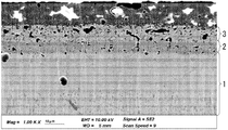
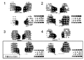
- FIG. 1a is a photograph of a cross-sectional structure of the solder alloy of the present invention, pre-soldered and soldered.
- the composition of the preliminary solder was 91.853Sn-8.14Zn-0.0070Mn (% by weight), and soldering was performed at a tip setting temperature of 250 ° C.
- the composition shows the solder layer 1 made of Sn—Zn composition, the bonding interface layer 2 made of AgZn intermetallic compound, and the electrode layer 3 made of Ag from the lower layer.
- the test piece is 8 ⁇ 8 ⁇ 3 mm, the thickness of the Ag layer is 20 ⁇ m, and the terminal is a 4 ⁇ 7 ⁇ 0.4 mm size pure copper surface plated with Sn. Added 4.5 x 7.5 x 0.2 mm in volume.
- the cycle of maintaining at ⁇ 30 ° C. for 30 minutes, raising the temperature to + 80 ° C. and maintaining for 30 minutes was repeated 1000 times.
- cracks could not be confirmed in a sample having an average particle diameter of AgZn intermetallic compound of 5 ⁇ m or less, whereas cracks were observed in samples having an average particle diameter of 20 ⁇ m and 10 ⁇ m.
- This experiment is based on the premise that when a void is present inside the interface, it develops into a crack by heat cycle.
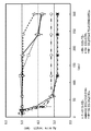
- FIG. 2 is a graph showing the results of immersing Ag wire having a diameter of 0.25 mm and a length of 10 mm in half in six kinds of solder baths having different compositions and measuring the residual length at regular intervals.
- the molten solder temperature is 300 ° C.
- sample 91Sn9Zn which is within the scope of the present invention, showed very good silver corrosion resistance.
- 93Sn7Zn and 92.99Sn7Zn0.01Mn also showed good silver corrosion resistance.
- about 2 mm was lost by eating after about 50 seconds. From this fact, it was confirmed that a solder composition containing 7 to 9% by weight of Zn using Sn as a base material exhibits good silver corrosion resistance.
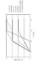
- the graph of FIG. 3 shows the results of a heat cycle test in which test pieces having seven kinds of compositions were repeated 90 cycles in the range of 90 ° to ⁇ 40 ° C.
- the test piece was a solder foil having a width of 5 mm, a length of 10 mm, and a thickness of 0.6 mm, and soldered to the surface of a silver electrode (foil thickness of about 15 ⁇ m) having a width of 50 mm, a length of 100 mm, and a thickness of 5 mm. Material was used.
- 93Sn7Zn with 92.992Sn7Zn0.008Mn to which Mn was added in a small amount, the Mn-added sample had fewer occurrences of cracks.
- the sample added with Mn had fewer cracks. From these relationships, it can be understood that, in the solder of Sn—Zn composition, the appearance of cracks can be reduced by using a solder alloy having a composition added with Mn to obtain a bonded product.
- the crack was confirmed by taking out the test piece during the heat cycle test, observing the soldered portion from the rear surface of the glass with a stereomicroscope (10 times), and counting the number of cracks detected on the glass surface. That is, by comparing the generated stress caused by the difference in thermal expansion coefficient between the glass containing the silver electrode and the solder, the strength of the joint interface was confirmed.
- the graph in FIG. 4 shows the results of a tensile test of test pieces having six types of compositions.
- the test method used was a test piece obtained by melting in an electric furnace and a graphite crucible at a liquidus temperature of + 100 ° C. and casting it in a mold at room temperature.
- the test piece was prepared to have a total length of 170 mm, a parallel part length of 60 mm, a width of 10 mm, and a thickness of 10 mm. It was.
- the measurement is based on JIS.
- the sample of 92.999Sn7Zn0.008Mn which is the scope of the present invention, showed the most suitable resistance to pulling.
- the graph of FIG. 5 shows the creep characteristics
- the test method was a test piece prepared in the same manner as in FIG. 4 with a load of 30 kg under a temperature atmosphere of 100 ° C. The test was conducted one by one. The distance between the scores is 50 mm. As a result, similar to the tensile test result of FIG. 4, the test piece to which Mn was added showed the best creep characteristics.
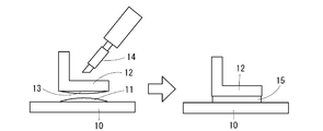
- FIG. 6 is a schematic diagram illustrating the case where the preliminary solder having the composition described above is performed, where 10 is an Ag electrode provided on the surface of the glass plate, 11 is a preliminary solder on the Ag electrode 10 side, The plated material, 12 is a Cu alloy terminal, 13 is a pre-solder provided on the joint surface of the Cu alloy terminal, and is similarly subjected to solder plating. 14 is a soldering iron. As a process, as shown in FIG. 6a, the soldering iron 14 is brought into contact with the back side of the solder plating of the Cu alloy terminal 12 and heated to about 250.degree. Then, both solder platings are melted, and solder joints 15 are formed as shown in FIG. 6b. In FIG.
- FIG. 7 is a transmission photograph that was irradiated with X-rays to confirm the internal state of the solder joint. In the specimen subjected to preliminary soldering, almost no voids were observed, but preliminary soldering was performed. None of the samples showed multiple voids for all samples.
Abstract
Description

試験の結果、AgZn金属間化合物の平均粒径が5μm以下の試料ではクラックを確認することができなかったのに対して、平均粒径20μm、10μmの試料ではクラックを観察した。なお、この実験は、ボイドを界面内部に有する場合には、ヒートサイクルによってクラックに発展することを前提としている。 The test piece is 8 × 8 × 3 mm, the thickness of the Ag layer is 20 μm, and the terminal is a 4 × 7 × 0.4 mm size pure copper surface plated with Sn. Added 4.5 x 7.5 x 0.2 mm in volume. In the heat cycle, the cycle of maintaining at −30 ° C. for 30 minutes, raising the temperature to + 80 ° C. and maintaining for 30 minutes was repeated 1000 times.
As a result of the test, cracks could not be confirmed in a sample having an average particle diameter of AgZn intermetallic compound of 5 μm or less, whereas cracks were observed in samples having an average particle diameter of 20 μm and 10 μm. This experiment is based on the premise that when a void is present inside the interface, it develops into a crack by heat cycle.
2 接合界面層
3 Ag電極層
10 Ag電極
11・13 はんだめっき
12 Cu合金端子
15 接合部 1
Claims (6)
- Zn2~9重量%、Mn0.0001~0.1重量%、残部Snからなるはんだ合金で、少なくとも表面層がAgである接合物を接合した接合物であって、前記接合物の表面層であるAgとはんだ合金中のZnによって形成されるAgZn金属間化合物の粒径が5μm以下である接合界面を有するはんだ接合物。 A solder alloy composed of 2 to 9% by weight of Zn, 0.0001 to 0.1% by weight of Mn, and the remaining Sn, and is a joined product in which a joined product having at least a surface layer of Ag is joined, and is a surface layer of the joined product. A solder joint having a joint interface in which a particle diameter of an AgZn intermetallic compound formed by Ag and Zn in a solder alloy is 5 μm or less.
- 2つの接合物の接合面双方に予め同一の前記はんだ合金組成のはんだめっきを施し、該はんだめっき同士を接触させながらはんだめっきを加熱溶融して凝固させた請求項1記載のはんだ接合物。 2. The solder joint according to claim 1, wherein solder joints of the same solder alloy composition are preliminarily applied to both joint surfaces of the two joints, and the solder plating is heated and melted and solidified while contacting the solder platings.
- [規則91に基づく訂正 25.03.2014]
加熱溶融の温度は230~300℃である請求項2記載のはんだ接合物。 [Correction 25.03.2014 under Rule 91]
The solder joint according to claim 2, wherein the temperature of heat melting is 230 to 300 ° C. - 少なくとも表面層がAgである2つの接合物の接合面双方に、Zn2~9重量%、Mn0.0001~0.1重量%、残部Snからなるはんだを予めめっきし、該はんだめっき同士を接触させながらはんだめっきを加熱溶融して凝固させるはんだ接合方法。 At least both of the joint surfaces of two joints whose surface layer is Ag are pre-plated with a solder composed of 2 to 9% by weight of Zn, 0.0001 to 0.1% by weight of Mn and the remaining Sn, and the solder platings are brought into contact with each other. Solder joining method that melts and solidifies solder plating while heating.
- 請求項4の接合方法において、接合物の表面層であるAgとはんだ合金中のZnによって形成されるAgZn金属間化合物の粒径が5μm以下となるように接合するはんだ接合方法。 5. The soldering method according to claim 4, wherein the AgZ intermetallic compound formed by Ag which is a surface layer of the joined product and Zn in the solder alloy is joined so that the particle diameter of the AgZn intermetallic compound is 5 μm or less.
- 請求項4又は5の接合方法において、加熱溶融の温度は230~300℃であるはんだ接合方法。 The soldering method according to claim 4 or 5, wherein the temperature of heat melting is 230 to 300 ° C.
Priority Applications (4)
| Application Number | Priority Date | Filing Date | Title |
|---|---|---|---|
| US14/775,013 US10329642B2 (en) | 2013-03-13 | 2014-03-12 | Solder alloy and joint thereof |
| CN201480014413.3A CN105189003A (en) | 2013-03-13 | 2014-03-12 | Solder alloy and joint thereof |
| EP14762700.4A EP2974818B1 (en) | 2013-03-13 | 2014-03-12 | Solder joining method |
| JP2015505504A JPWO2014142153A1 (en) | 2013-03-13 | 2014-03-12 | Solder joint and solder joint method |
Applications Claiming Priority (2)
| Application Number | Priority Date | Filing Date | Title |
|---|---|---|---|
| JP2013050758 | 2013-03-13 | ||
| JP2013-050758 | 2013-03-13 |
Publications (1)
| Publication Number | Publication Date |
|---|---|
| WO2014142153A1 true WO2014142153A1 (en) | 2014-09-18 |
Family
ID=51536804
Family Applications (1)
| Application Number | Title | Priority Date | Filing Date |
|---|---|---|---|
| PCT/JP2014/056440 WO2014142153A1 (en) | 2013-03-13 | 2014-03-12 | Solder alloy and joint thereof |
Country Status (5)
| Country | Link |
|---|---|
| US (1) | US10329642B2 (en) |
| EP (1) | EP2974818B1 (en) |
| JP (2) | JPWO2014142153A1 (en) |
| CN (1) | CN105189003A (en) |
| WO (1) | WO2014142153A1 (en) |
Cited By (1)
| Publication number | Priority date | Publication date | Assignee | Title |
|---|---|---|---|---|
| WO2016119096A1 (en) * | 2015-01-29 | 2016-08-04 | 苏州天兼新材料科技有限公司 | Lead-free welding material and method for preparing scaling powder thereof |
Families Citing this family (1)
| Publication number | Priority date | Publication date | Assignee | Title |
|---|---|---|---|---|
| CN105499738B (en) * | 2016-01-21 | 2017-12-29 | 深圳市科美达自动化设备有限公司 | The tin-soldering method of carbon brush motor rotor commutator pin |
Citations (5)
| Publication number | Priority date | Publication date | Assignee | Title |
|---|---|---|---|---|
| JP2000015478A (en) | 1998-06-30 | 2000-01-18 | Toshiba Corp | Soldering material |
| JP2000280066A (en) | 1999-03-31 | 2000-10-10 | Toshiba Corp | Forming method of non-lead jointing member |
| JP2002217434A (en) * | 2001-01-19 | 2002-08-02 | Sharp Corp | Solar cell, interconnector and string for the solar cell |
| US20040208779A1 (en) * | 2001-07-05 | 2004-10-21 | Ika Consulting Ltd. | Lead-free alloy |
| JP2011156558A (en) | 2010-01-30 | 2011-08-18 | Nihon Superior Co Ltd | Lead-free solder alloy |
Family Cites Families (22)
| Publication number | Priority date | Publication date | Assignee | Title |
|---|---|---|---|---|
| JPS55128396A (en) * | 1979-03-26 | 1980-10-04 | Packer Eng Ass | Zn alloy wax and its use |
| US4816219A (en) * | 1986-07-18 | 1989-03-28 | Nihon Speriasha Co., Ltd. | Low-temperature solder composition |
| US5066544A (en) * | 1990-08-27 | 1991-11-19 | U.S. Philips Corporation | Dispersion strengthened lead-tin alloy solder |
| US5417771A (en) * | 1994-02-16 | 1995-05-23 | Takeda Chemical Industries, Ltd. | Soldering flux |
| JPH07246493A (en) * | 1994-03-09 | 1995-09-26 | Nippon Superia Shiya:Kk | Solder alloy |
| JP2000197988A (en) * | 1998-03-26 | 2000-07-18 | Nihon Superior Co Ltd | Leadless solder alloy |
| KR100377232B1 (en) * | 1998-03-26 | 2003-03-26 | 니혼 슈페리어 샤 가부시키 가이샤 | Leadless Solder |
| TW516984B (en) * | 1999-12-28 | 2003-01-11 | Toshiba Corp | Solder material, device using the same and manufacturing process thereof |
| JP3221670B2 (en) * | 2000-02-24 | 2001-10-22 | 株式会社日本スペリア社 | Copper concentration control method for dip solder bath |
| TW592872B (en) * | 2001-06-28 | 2004-06-21 | Senju Metal Industry Co | Lead-free solder alloy |
| JP2004114124A (en) * | 2002-09-27 | 2004-04-15 | Hitachi Metals Ltd | Electronic part and its manufacturing method |
| GB2421030B (en) * | 2004-12-01 | 2008-03-19 | Alpha Fry Ltd | Solder alloy |
| CN101053932A (en) * | 2007-05-31 | 2007-10-17 | 上海交通大学 | Improved type Sn-Ag-Zn lead-free solder for inhibiting solid state interface reaction |
| WO2009051181A1 (en) * | 2007-10-19 | 2009-04-23 | Nihon Superior Sha Co., Ltd. | Lead-free solder alloy |
| TW201210733A (en) * | 2010-08-26 | 2012-03-16 | Dynajoin Corp | Variable melting point solders |
| JP2014096198A (en) * | 2011-03-02 | 2014-05-22 | Central Glass Co Ltd | Method of bonding window pane for automobiles and feeding terminal |
| WO2012137901A1 (en) * | 2011-04-08 | 2012-10-11 | 株式会社日本スペリア社 | Solder alloy |
| WO2012141331A1 (en) * | 2011-04-15 | 2012-10-18 | 株式会社日本スペリア社 | Lead-free solder alloy |
| JP5724638B2 (en) * | 2011-05-30 | 2015-05-27 | 日立金属株式会社 | Pb-free solder, solder-coated conductor, and electrical parts using the same |
| US8783544B2 (en) * | 2012-03-20 | 2014-07-22 | Joseph W. Harris | Brazing alloys and methods of brazing |
| DE112013007179T5 (en) * | 2013-06-20 | 2016-04-28 | Mitsubishi Electric Corporation | Zn-based lead-free solder and semiconductor power module |
| GB201312388D0 (en) * | 2013-07-10 | 2013-08-21 | Cambridge Entpr Ltd | Materials and methods for soldering and soldered products |
-
2014
- 2014-03-12 JP JP2015505504A patent/JPWO2014142153A1/en active Pending
- 2014-03-12 CN CN201480014413.3A patent/CN105189003A/en active Pending
- 2014-03-12 WO PCT/JP2014/056440 patent/WO2014142153A1/en active Application Filing
- 2014-03-12 US US14/775,013 patent/US10329642B2/en active Active
- 2014-03-12 EP EP14762700.4A patent/EP2974818B1/en not_active Not-in-force
-
2019
- 2019-03-22 JP JP2019054759A patent/JP6688417B2/en not_active Expired - Fee Related
Patent Citations (6)
| Publication number | Priority date | Publication date | Assignee | Title |
|---|---|---|---|---|
| JP2000015478A (en) | 1998-06-30 | 2000-01-18 | Toshiba Corp | Soldering material |
| JP2000280066A (en) | 1999-03-31 | 2000-10-10 | Toshiba Corp | Forming method of non-lead jointing member |
| JP2002217434A (en) * | 2001-01-19 | 2002-08-02 | Sharp Corp | Solar cell, interconnector and string for the solar cell |
| US20040208779A1 (en) * | 2001-07-05 | 2004-10-21 | Ika Consulting Ltd. | Lead-free alloy |
| US6936219B2 (en) | 2001-07-05 | 2005-08-30 | Ika Industrial Consulting Ltd. | Lead-free alloy |
| JP2011156558A (en) | 2010-01-30 | 2011-08-18 | Nihon Superior Co Ltd | Lead-free solder alloy |
Cited By (1)
| Publication number | Priority date | Publication date | Assignee | Title |
|---|---|---|---|---|
| WO2016119096A1 (en) * | 2015-01-29 | 2016-08-04 | 苏州天兼新材料科技有限公司 | Lead-free welding material and method for preparing scaling powder thereof |
Also Published As
| Publication number | Publication date |
|---|---|
| EP2974818A1 (en) | 2016-01-20 |
| JPWO2014142153A1 (en) | 2017-02-16 |
| JP2019136776A (en) | 2019-08-22 |
| CN105189003A (en) | 2015-12-23 |
| JP6688417B2 (en) | 2020-04-28 |
| EP2974818B1 (en) | 2019-01-16 |
| EP2974818A4 (en) | 2016-09-28 |
| US10329642B2 (en) | 2019-06-25 |
| US20160032424A1 (en) | 2016-02-04 |
Similar Documents
| Publication | Publication Date | Title |
|---|---|---|
| JP5943066B2 (en) | Bonding method and manufacturing method of bonded structure | |
| WO2018174162A1 (en) | Solder joint | |
| JPH1034376A (en) | Lead-free solder | |
| EP3828294B1 (en) | Lead-free solder alloy and solder joint part | |
| JP2006255784A (en) | Unleaded solder alloy | |
| JP4135268B2 (en) | Lead-free solder alloy | |
| JP4618089B2 (en) | Sn-In solder alloy | |
| JP2013000744A (en) | Lead-free solder alloy, and soldered joint using the same | |
| JP6688417B2 (en) | Solder joining method | |
| JP6135885B2 (en) | Solder alloy and mounting structure using the same | |
| EP3590652B1 (en) | Solder alloy, solder junction material, and electronic circuit substrate | |
| JP6548537B2 (en) | Solder alloy and solder composition | |
| JP3878978B2 (en) | Lead-free solder and lead-free fittings | |
| JP7287606B2 (en) | Lead-free solder alloy | |
| EP3369520B1 (en) | Solder alloy for preventing fe erosion, resin flux cored solder, wire solder, resin flux cored wire solder, flux coated solder, solder joint and soldering method | |
| WO2007014530A1 (en) | Lead-free sn-ag-cu-ni-al system solder alloy | |
| JP2016172286A (en) | Solder for aluminum, and solder joint | |
| JP6887183B1 (en) | Solder alloys and molded solders | |
| JP4359983B2 (en) | Electronic component mounting structure and manufacturing method thereof | |
| JP2008130697A (en) | Solder bonding structure and manufacturing method thereof | |
| WO2016185674A1 (en) | Solder alloy and package structure using same | |
| TW201350250A (en) | Solder alloy | |
| JP2008093701A (en) | Solder alloy | |
| JP2006000925A (en) | Lead-free solder alloy and producing method thereof | |
| JP6389553B2 (en) | Aluminum solder and solder joints |
Legal Events
| Date | Code | Title | Description |
|---|---|---|---|
| WWE | Wipo information: entry into national phase |
Ref document number: 201480014413.3 Country of ref document: CN |
|
| 121 | Ep: the epo has been informed by wipo that ep was designated in this application |
Ref document number: 14762700 Country of ref document: EP Kind code of ref document: A1 |
|
| DPE2 | Request for preliminary examination filed before expiration of 19th month from priority date (pct application filed from 20040101) | ||
| ENP | Entry into the national phase |
Ref document number: 2015505504 Country of ref document: JP Kind code of ref document: A |
|
| WWE | Wipo information: entry into national phase |
Ref document number: 2014762700 Country of ref document: EP |
|
| WWE | Wipo information: entry into national phase |
Ref document number: 14775013 Country of ref document: US |
|
| NENP | Non-entry into the national phase |
Ref country code: DE |