WO2014141838A1 - 有機半導体膜の形成方法 - Google Patents
有機半導体膜の形成方法 Download PDFInfo
- Publication number
- WO2014141838A1 WO2014141838A1 PCT/JP2014/053930 JP2014053930W WO2014141838A1 WO 2014141838 A1 WO2014141838 A1 WO 2014141838A1 JP 2014053930 W JP2014053930 W JP 2014053930W WO 2014141838 A1 WO2014141838 A1 WO 2014141838A1
- Authority
- WO
- WIPO (PCT)
- Prior art keywords
- organic semiconductor
- substrate
- semiconductor film
- cover member
- forming
- Prior art date
- Legal status (The legal status is an assumption and is not a legal conclusion. Google has not performed a legal analysis and makes no representation as to the accuracy of the status listed.)
- Ceased
Links
Images

Classifications
-
- H—ELECTRICITY
- H10—SEMICONDUCTOR DEVICES; ELECTRIC SOLID-STATE DEVICES NOT OTHERWISE PROVIDED FOR
- H10K—ORGANIC ELECTRIC SOLID-STATE DEVICES
- H10K71/00—Manufacture or treatment specially adapted for the organic devices covered by this subclass
- H10K71/10—Deposition of organic active material
- H10K71/12—Deposition of organic active material using liquid deposition, e.g. spin coating
- H10K71/15—Deposition of organic active material using liquid deposition, e.g. spin coating characterised by the solvent used
-
- H—ELECTRICITY
- H10—SEMICONDUCTOR DEVICES; ELECTRIC SOLID-STATE DEVICES NOT OTHERWISE PROVIDED FOR
- H10K—ORGANIC ELECTRIC SOLID-STATE DEVICES
- H10K71/00—Manufacture or treatment specially adapted for the organic devices covered by this subclass
- H10K71/10—Deposition of organic active material
- H10K71/191—Deposition of organic active material characterised by provisions for the orientation or alignment of the layer to be deposited
-
- H—ELECTRICITY
- H10—SEMICONDUCTOR DEVICES; ELECTRIC SOLID-STATE DEVICES NOT OTHERWISE PROVIDED FOR
- H10K—ORGANIC ELECTRIC SOLID-STATE DEVICES
- H10K71/00—Manufacture or treatment specially adapted for the organic devices covered by this subclass
- H10K71/20—Changing the shape of the active layer in the devices, e.g. patterning
-
- H—ELECTRICITY
- H10—SEMICONDUCTOR DEVICES; ELECTRIC SOLID-STATE DEVICES NOT OTHERWISE PROVIDED FOR
- H10K—ORGANIC ELECTRIC SOLID-STATE DEVICES
- H10K10/00—Organic devices specially adapted for rectifying, amplifying, oscillating or switching; Organic capacitors or resistors having potential barriers
- H10K10/40—Organic transistors
- H10K10/46—Field-effect transistors, e.g. organic thin-film transistors [OTFT]
- H10K10/462—Insulated gate field-effect transistors [IGFETs]
- H10K10/484—Insulated gate field-effect transistors [IGFETs] characterised by the channel regions
-
- H—ELECTRICITY
- H10—SEMICONDUCTOR DEVICES; ELECTRIC SOLID-STATE DEVICES NOT OTHERWISE PROVIDED FOR
- H10K—ORGANIC ELECTRIC SOLID-STATE DEVICES
- H10K71/00—Manufacture or treatment specially adapted for the organic devices covered by this subclass
-
- H—ELECTRICITY
- H10—SEMICONDUCTOR DEVICES; ELECTRIC SOLID-STATE DEVICES NOT OTHERWISE PROVIDED FOR
- H10K—ORGANIC ELECTRIC SOLID-STATE DEVICES
- H10K71/00—Manufacture or treatment specially adapted for the organic devices covered by this subclass
- H10K71/80—Manufacture or treatment specially adapted for the organic devices covered by this subclass using temporary substrates
-
- H—ELECTRICITY
- H10—SEMICONDUCTOR DEVICES; ELECTRIC SOLID-STATE DEVICES NOT OTHERWISE PROVIDED FOR
- H10K—ORGANIC ELECTRIC SOLID-STATE DEVICES
- H10K99/00—Subject matter not provided for in other groups of this subclass
Definitions
- the present invention relates to a method for forming an organic semiconductor film used for a thin film transistor using an organic semiconductor material.
- Organic semiconductor materials can be used in devices that use logic circuits such as TFTs (thin film transistors), RFIDs (RF tags) and memories used in liquid crystal displays and organic EL displays because they can be reduced in weight, cost, and flexibility.
- An organic semiconductor element having an organic semiconductor film (organic semiconductor layer) made of is used.
- an organic semiconductor film As one method for forming an organic semiconductor film, there is a wet method in which an organic semiconductor film is formed by applying a paint obtained by dissolving an organic semiconductor material in a solvent to a substrate and drying the solution.
- This method of forming a wet organic semiconductor film has various advantages such that an organic semiconductor film can be formed at low cost, and an organic semiconductor film can be formed corresponding to a large area.
- Patent Document 1 a frame is formed so as to surround the formation position of an organic semiconductor film on a substrate, a solution in which an organic semiconductor material is dissolved is filled in the frame, and the solution is dried. Describes a method of forming an organic semiconductor crystal.
- Patent Document 2 uses a contact member having a contact surface to which a solution in which an organic semiconductor material is dissolved is attached, and the contact member is disposed so that the contact surface has a certain relationship with the surface of the substrate.
- a method of forming a crystalline organic semiconductor film by holding a solution on a contact surface of a contact member and drying the solution is described.
- a crystalline organic semiconductor film is formed by using a contact member having a contact surface standing upright to a substrate, filling a solution in a corner formed by the contact surface and the substrate, and drying the solution. How to do is described.
- a contact member having a contact surface inclined with respect to the substrate is used, the contact surface and the substrate are arranged at a predetermined interval, and the contact surface and the substrate are disposed on both sides.
- a method for forming a crystalline organic semiconductor film by filling a solution by contact and drying is also described.
- an organic semiconductor film having crystallinity can be formed.
- the demand for the formation of an organic semiconductor film in recent years has become more severe, and the emergence of a method that can stably form an organic semiconductor film that has a better crystallinity and can provide a semiconductor device with high mobility. Is desired.
- An object of the present invention is to solve such problems of the prior art, and a method for forming an organic semiconductor film that can stably form an organic semiconductor film having good crystallinity and high mobility. It is to provide.
- the organic semiconductor film forming method of the present invention uses a solution in which an organic semiconductor material is dissolved to form an organic semiconductor film made of an organic semiconductor material.
- a cover member that is disposed on the substrate on which the organic semiconductor film is formed and forms a space between the substrate, the solution is filled in the space between the cover member and the substrate, and the filled solution is dried.
- the cover member has a regulation surface in which an uppermost part farthest from the substrate and descending parts provided on both sides in the y direction of the uppermost part from the uppermost part to the substrate are formed, and the regulation surface is formed.
- the x direction orthogonal to the y direction of the space is a shape that opens, and is arranged with the regulating surface facing the substrate and the entire area of at least one end in the y direction contacting the substrate, Further, when the y-direction end that contacts the substrate over the entire area of the cover member is the base end, at least part of the solution in the y-direction end opposite to the base end on the regulation surface is from the base end.
- the shortest line that is located at a location that does not exceed the uppermost portion of the regulation surface when viewed, and that connects the base end and the separation position where the solution is most separated from the base end in the y direction on the regulation surface;
- the apparent angle which is the angle formed by the point where the perpendicular drawn from the separation position to the substrate intersects the substrate and the shortest line connecting the base ends, is 50 ° or less, and the length in the x direction is set to the y direction.
- the surface area of the portion of the solution not in contact with the substrate and the cover member is preferably 35% or less of the surface area of the entire solution.
- substrate and cover member of a solution is 1% or more of the surface area of the whole solution.
- the apparent angle is preferably 3 ° or more.
- x / y ratio is 100,000 or less.
- the cover member is disposed with both end portions in the y direction contacting the substrate.
- the cover member is disposed so that the entire area of both end portions in the y direction is in contact with the substrate.
- a cover member is plate shape.
- the cover member has a region parallel to both end portions in the y direction.
- the evaporation of the solvent is appropriately controlled, and the organic semiconductor film having good crystallinity is stably formed. be able to.
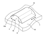
- FIG. 1 A perspective view which shows notionally an example of the formation method of the organic-semiconductor film of this invention.
- FIG. 1 A perspective view of the formation method of the organic-semiconductor film shown in FIG. 1
- B is a top view of the formation method of the organic-semiconductor film shown in FIG.
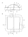
- A) is a front view of another example of the method for forming an organic semiconductor film of the present invention
- FIG. (B) is a plan view.
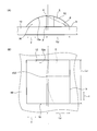
- A)-(I) is a figure which shows notionally another example of the formation method of the organic-semiconductor film of this invention. It is a conceptual diagram for demonstrating the formation method of the organic-semiconductor film of this invention.
- FIG. 1 and 2 conceptually show an example of a method for forming an organic semiconductor film of the present invention.
- 2A is a front view of FIG. 1 viewed from the direction of arrow x
- FIG. 2B is a plan view of FIG. 1 viewed from above.
- the method for forming an organic semiconductor film of the present invention forms an organic semiconductor film using a solution obtained by dissolving an organic semiconductor material to be an organic semiconductor film in a solvent.
- the organic semiconductor film forming method of the present invention includes a cover member 12 that forms a space 16 with a substrate 10 on a substrate 10 on which the organic semiconductor film is formed.
- the space 16 is filled with a solution obtained by dissolving an organic semiconductor material to be an organic semiconductor film in a solvent (hereinafter referred to as a coating solution E) so as to be in contact with the substrate 10 and the cover member 12.
- the coating liquid E is dried, and then the cover member 12 is removed to form an organic semiconductor film.
- the substrate 10 has an organic semiconductor film formed on the surface thereof. That is, the substrate 10 is a substrate of an organic semiconductor element.
- a plate-like material (sheet-like material / film) made of various materials such as metals such as silicon, ceramics, glass, and plastics. ) Is available.
- the substrate on which the organic semiconductor film is formed in addition to a simple plate-like material as shown in the drawing, materials having various configurations that can be used for manufacturing an organic semiconductor element can be used.
- the substrate may be one in which an insulating layer is formed on the entire surface or a part of the surface of the support (semiconductor element substrate).
- a gate electrode is formed on the support, and the support and the gate electrode are formed.
- An insulating layer may be formed so as to be covered, or an insulating layer may be formed on the surface of a support serving as a gate electrode, and a source electrode and a drain electrode may be formed thereon.
- the organic semiconductor film forming method of the present invention can be applied to various known organic semiconductor elements such as bottom gate-bottom contact type, top gate-bottom contact type, bottom gate-top contact type, top gate-bottom contact type. It can be used for forming an organic semiconductor film (organic semiconductor layer) in a manufacturing process.
- organic semiconductor film organic semiconductor layer
- various types exemplified by the above-described substrate 10 can be used as a support body of these substrates.
- the cover member 12 forms a space for filling the coating liquid E to be an organic semiconductor film with the surface of the substrate 10 on which the organic semiconductor film is formed (hereinafter also referred to as the surface) (that is, coating of the coating liquid E).
- the region is regulated), and the drying of the coating liquid E (solvent evaporation) is controlled.
- the cover member has an uppermost portion that is farthest from the surface of the substrate 10 and a descending portion that is provided on both sides of the uppermost portion in the direction of the arrow y and faces the surface of the substrate 10 from the uppermost portion.
- the control surface is disposed with the control surface facing the substrate 10. Further, the space formed by the restriction surface of the cover member together with the surface of the substrate 10 is open in the x direction orthogonal to the y direction.
- the cover member 12 has a shape formed by curving a square plate material (sheet-like material / film) into an arc shape (cylindrical circumferential surface shape).
- the concave surface of the circular arc becomes the regulating surface 12a.
- the cover member 12 is placed on the surface of the substrate 10 with the circumferential direction of the arc (the direction perpendicular to the center line) as the y direction and the concave surface that is the regulating surface 12a facing the substrate 10. Therefore, the x direction orthogonal to the y direction is parallel to the center line of this arc (in FIG. 2A, the x direction is perpendicular to the paper surface). Further, the cover member 12 is disposed so that the entire area at both ends in the y direction is in contact with the surface of the substrate 10.
- the position indicated by the alternate long and short dash line in FIG. 2 is the uppermost portion of the cover member 12 (the uppermost portion of the arc). Therefore, the regulation surface 12a of the cover member 12 has a configuration in which a descending portion that faces the surface of the substrate 10 in an arc shape from the uppermost portion indicated by the alternate long and short dash line toward both sides in the y direction.
- the base end is the end in the y direction where the entire region contacts the surface of the substrate 10, and the base end side is filled with the coating liquid E.
- both end portions in the y direction of the regulation surface 12 a are in contact with the substrate 10 over the entire surface.
- the cover member 12 may have any end portion in the y direction as a base end.
- the right side in the figure is the base end b.
- the base member b side of the space 16 formed by the cover member 12 and the substrate 10 is brought into contact with the cover member 12 and the substrate 10 and filled with the coating liquid E.
- the coating liquid E is dried to form an organic semiconductor film.
- the coating liquid E is viewed from the base end b, at least a part of the end portion in the y direction opposite to the base end b on the regulation surface 12a does not exceed the uppermost portion, that is, the alternate long and short dash line. , The space 16 is filled.
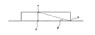
- the coating liquid E is a line in the y direction that connects the base end b and a position e where the coating liquid E is farthest from the base end b in the y direction on the regulation surface 12a (hereinafter also referred to as a separation position e).
- the apparent angle ⁇ which is an angle formed by a line in the y direction connecting the base p and the point p where the perpendicular line drawn from the separation position e to the substrate 10 intersects the substrate 10 and the base end b, is 50 ° or less.
- the space 16 is filled so as to be.
- the coating liquid E has a space such that the apex angle on the base end b side of the right triangle that forms a plane parallel to the y direction connecting the base end b, the separation position e, and the point p is 50 ° or less. 16 is filled. Further, the coating liquid E is filled in the space 16 so that the x / y ratio obtained by dividing the length Lx in the x direction by the length Ly in the y direction is 0.2 or more.
- the organic semiconductor film forming method of the present invention uses the cover member 12 having such a predetermined shape, and applies a coating solution in the space 16 formed by the substrate 10 and the cover member 12 so as to satisfy the above three conditions. E is filled, and the coating liquid E is dried to form an organic semiconductor film.
- the present invention increases the concentration of the solvent in the evaporation space of the coating liquid E, that is, the space 16 to reduce the evaporation rate of the solvent of the coating liquid E, that is, the drying speed.
- the drying speed of the coating liquid E can be suitably adjusted. Therefore, according to the method for forming an organic semiconductor film of the present invention, it is possible to appropriately control the drying of the coating liquid E, to obtain a high-quality organic semiconductor that has favorable crystallinity and crystal size and has a low defect frequency. Can be formed.
- the liquid surface of the coating liquid E filled in the space 16 is shown as a plane for the sake of simplicity of the drawings and description.
- the liquid level is not necessarily flat, and often has a convex shape or a concave shape.
- the liquid surface opposite to the base end b in the y direction may be convex.
- the liquid surface may be concave.
- a position that is the most distant from the base end b in the y direction is set as a separation position e.
- the coating liquid E is transferred to the base end on the regulation surface 12a. It is not necessary to be positioned closer to the base end b side than the uppermost portion of the regulation surface 12a when viewed from the b side. That is, in the present invention, as shown in FIG. 3, the coating liquid E is partly on the base end b side in the y direction with respect to the base end b, as viewed from the base end b. If located, there may be a region exceeding the uppermost portion in the y direction when viewed from the base end b.
- the restricting surface 12a of the cover member 12 extends in the y direction from the uppermost portion on the uppermost portion that is farthest from the substrate 10 and on both sides of the uppermost portion in the y direction. And a descending portion toward the surface. That is, the regulation surface 12a of the cover member 12 has a region that descends from the top to the substrate 10 on the other side of the top when viewed in the y direction from the base end b filled with the coating liquid E. .
- Such a regulating surface 12a of the cover member 12 forms, together with the substrate 10, a convex space 16 having the top as a vertex toward the top (the opposite side to the substrate 10). Therefore, the solvent evaporated from the coating liquid E stays in the convex space 16, and as a result, the solvent concentration in the space 16 can be increased and the drying speed of the coating liquid E can be reduced.
- the end surface in the x direction of the space 16 formed by the substrate 10 and the cover member 12 may be partially open, but it is preferable that the entire surface is open as in the illustrated example. Thereby, the controllability of drying of the coating liquid E can be further improved by the apparent angle ⁇ and the x / y ratio, and further by the contact area ratio with the outside air described later.
- the coating liquid E filling the space 16 is filled such that at least a part thereof does not exceed the uppermost portion when viewed from the base end b on the regulation surface 12a.
- the coating liquid E is opposite to the base end b in the y direction. Will flow to the end of the side. Therefore, the coating liquid E is applied to a position different from the base end b side of the space 16, that is, the place where the organic semiconductor film is formed, and the organic semiconductor film cannot be formed at the target position.
- a line connecting the base end b and the separation position e (two-dot chain line) and a line connecting the point p where the perpendicular line from the separation position e intersects the substrate 10 and the base end b are formed.
- the apparent angle ⁇ formed is an apparent angle at the base end b of the coating liquid E filling the space 16.
- the space 16 is filled with the coating liquid E so that the apparent angle ⁇ is 50 ° or less.
- the apparent angle ⁇ exceeds 50 °, the contact area of the coating liquid E with the outside air becomes too large, the drying speed of the coating liquid E becomes too fast, and the crystallinity of the organic semiconductor is lowered.
- the apparent angle is preferably 40 ° or less, more preferably 30 ° or less, and particularly preferably 20 ° or less.
- the apparent angle ⁇ only needs to exceed 0 °.
- the smaller the apparent angle ⁇ the slower the drying of the coating solution, so that the productivity is lowered and fine crystals are likely to be formed in the formed organic semiconductor film.
- the apparent angle ⁇ is preferably 3 ° or more, more preferably 5 ° or more, and particularly preferably 10 ° or more.
- the coating liquid E is filled in the space 16 so that the x / y ratio obtained by dividing the length Lx in the x direction of the coating liquid by the length Ly in the y direction is 0.2 or more. If the x / y ratio is less than 0.2, the contact area of the coating liquid E with the outside air becomes too large, the drying speed of the coating liquid E becomes too fast, and the crystallinity of the organic semiconductor decreases. Considering this point, the x / y ratio is preferably 0.2 or more, more preferably 0.3 or more, and particularly preferably 0.45 or more.
- the x / y ratio may be large considering the case where a large number of organic semiconductor elements are formed corresponding to the manufacture of TFTs (thin film transistors) for display.
- the x / y ratio is preferably 100,000 or less, more preferably 10,000 or less, further preferably 1000 or less, and particularly preferably 100 or less.
- the length Ly of the coating liquid E in the y direction is the position farthest from the base end b in the y direction on the substrate 10.
- the distance in the y direction between the base end b and the coating liquid E is defined as the length Ly of the coating liquid E in the y direction.
- the length Lx in the x direction of the coating liquid E is the distance in the x direction at the position where the liquid surface is most separated in the x direction on the substrate 10, and the length is the length Lx in the x direction.
- the surface area of the coating liquid E that is in contact with the outside air that is, the surface area of the coating liquid E that is not in contact with the substrate 10 and the cover member 12 is 35% or less of the entire surface area of the coating liquid E. It is preferably 32% or less, more preferably 30% or less, even more preferably 20% or less.
- the surface area of the coating liquid E in contact with the outside air is preferably 1% or more of the surface area of the coating liquid, more preferably 5% or more, more preferably 10% or more, and particularly preferably 15% or more is preferable.
- the liquid surface of the coating liquid E is not necessarily flat, and often has a concave or convex shape. Therefore, it is very difficult to accurately calculate the surface area of the coating liquid. is there. Therefore, in the present invention, the liquid surface opposite to the base end b in the y direction of the coating liquid E is regarded as a planar shape parallel to the x direction at a position where the base end b and the coating liquid E are most separated in the y direction. . Further, the liquid surface of the coating liquid E on both sides in the x direction is a plane parallel to the y direction connecting the base end b, the separation position e, and the point p using the liquid surface in the y direction set in this way. As a right triangle. In the present invention, the surface area of the apparent coating liquid E calculated using the liquid level set in this way is defined as the surface area of the coating liquid E.
- the cover member has a convex space as described above in addition to the arc shape in which both ends of the regulating surface 12a in the y direction are in contact with the substrate 10 as shown in the illustrated example. As long as it can be formed, various shapes can be used. Further, the cover member can be disposed on the substrate 10 in various states.
- the arc-shaped cover member may be configured such that one end in the y direction does not contact the substrate 10.
- the horizontal direction in the figure is the y direction.
- the side of the cover member that is not in contact with the substrate 10 may be supported by a columnar member. Or you may suspend and support the side which is not contacting the board
- the cover member is such that both ends in the y direction are in contact with the substrate 10 in that the solvent concentration in the evaporation space of the coating liquid E can be suitably increased and the evaporation of the coating liquid E can be easily controlled.
- it is more preferable that the entire area at both ends in the y direction is in contact with the substrate 10.
- one end portion in the y direction contacts the entire substrate 10 and the other end portion. May be configured such that a part thereof does not contact the substrate 10 but partially contacts the substrate 10.
- one end in the y direction contacts the entire substrate 10 and the other one
- the end may have a rectangular notch, and the end other than the notch may be in contact with the substrate 10.
- the cutout may have various shapes such as a triangle and a circle in addition to the rectangle. Further, the notch may be formed not at the center in the x direction but at the end.
- the cover member may have a trapezoidal shape as conceptually shown in FIGS. 4 (E) and (F). Since the cover member has regions parallel to both ends in the y direction, such as the square shown in FIG. 1, the trapezoid, or the rectangle, both ends in the y direction of the cover member can be easily brought into contact with the substrate 10. Preferably, the entire area at both ends in the y direction can contact the substrate 10.
- the cover member does not have to have a shape having a descending portion that gradually approaches the substrate 10 on both sides in the y direction from the uppermost portion as in the above example.
- the cover member having a shape in which the end portion of the rectangular parallelepiped is bent at a right angle (ie, a cube shape in which one side of the maximum surface and two opposite side surfaces are opened) is bent.
- the configuration may be such that the bent end is in contact with the substrate 10 with the side as the y direction.
- the uppermost portion is planar, and the portion bent at a right angle is the descending portion.
- the upper surface may be inclined in a triangular shape as conceptually shown in FIG. 4 (H), not in a planar shape as shown in FIG. 4 (G), and further in FIG. 4 (I). As shown specifically, it may be configured to have a portion inclined toward the substrate 10 on one side of the descending portion.
- the apparent angle ⁇ described above is used.
- the line connecting the base end b and the separation position e farthest from the base end b in the y direction on the regulation surface and the perpendicular from the separation position e are the substrate.
- An angle formed by a point p intersecting 10 and a line connecting the base end b is defined as an apparent angle ⁇ .
- the cover member is not limited to the plate-like object as shown in the illustrated example, and various kinds of materials can be used as long as the restriction surface forming the convex space as described above is formed.
- a member of the shape can be used.
- a concave portion such as an arc column is formed on one surface of a block-shaped member such as a cube or a rectangular parallelepiped, and a space for filling a solution with the substrate 10 is formed using this surface as a regulating surface.
- the number of cover members disposed on the surface of the substrate 10 is not limited to one, and a plurality of cover members are disposed on the surface of one substrate to form an organic semiconductor film. Also good.
- one cover member may have a plurality of regulating surfaces corresponding to the formation of a plurality of organic semiconductor films.
- the cover member 12 can be formed of various materials. Specifically, polytetrafluoroethylene, polychlorotrifluoroethylene (trifluorinated resin, polyvinylidene fluoride, polyvinyl fluoride, fluorinated resin copolymer, perfluoroalkoxy fluororesin, tetrafluoroethylene / hexafluoropropylene
- a liquid-repellent material such as a copolymer, a fluororesin such as an ethylene / tetrafluoroethylene copolymer or an ethylene / chlorotrifluoroethylene copolymer, or a silicone resin is preferred.
- a material such as a resin coated with a liquid repellent resin or a liquid repellent treatment is preferably used as the cover member 12.
- the size of the cover member 12 may be appropriately determined according to the organic semiconductor film to be formed.
- the cover member 12 is disposed on the surface of the substrate 10, and the organic semiconductor film is formed on the base end b side of the space 16 formed by the surface of the substrate 10 and the cover member 12.
- An organic semiconductor film is formed on the surface of the substrate 10 by filling the coating liquid E obtained by dissolving the organic semiconductor material, drying the coating liquid E, and then removing the cover member 12.
- the cover member 12 before the cover member 12 is arrange
- Various surface treatments such as treatment may be performed.
- the organic semiconductor material various known materials that can be used for an organic semiconductor film formed by a so-called wet process (wet process) such as a coating method in the manufacture of an organic semiconductor element can be used.
- wet process such as a coating method in the manufacture of an organic semiconductor element
- Specific examples include pentacenes such as 6,13-bis (triisopropylsilylethynyl) pentacene (TIPS pentacene), rubrenes, fullerenes, phthalocyanines, TCNQs, and the like.
- TIPS pentacene 6,13-bis (triisopropylsilylethynyl) pentacene
- rubrenes fullerenes
- phthalocyanines phthalocyanines
- TCNQs phthalocyanines
- solvents can be used as the solvent contained in the coating liquid E as long as it can dissolve the organic semiconductor material to be used.
- the organic semiconductor material is an acene such as TIPS pentacene, toluene, anisole, n-butylbenzene, acetone and the like are preferably exemplified.
- the concentration of the organic semiconductor material in the coating liquid E may be set as appropriate according to the type of organic semiconductor material, the type of solvent, the thickness of the organic semiconductor film to be formed, the shape of the cover member 12, and the like.
- the coating liquid E may contain a surfactant, a polymer, or the like, if necessary, in addition to the organic semiconductor material and the solvent.
- the coating liquid E contains components other than such an organic semiconductor material and a solvent, it is preferable that the content shall be 50 mass% or less.
- Example 1 An n-type silicon substrate having a size of 20 ⁇ 20 mm and a thickness of 0.5 mm was prepared. The surface of this silicon substrate was heat-treated to form a thermal oxide film having a thickness of 300 nm. Furthermore, the surface of the thermal oxide film was irradiated with UV light to improve paintability.
- Teflon plate having a size of 16 ⁇ 16 mm and a thickness of 0.2 mm was prepared.
- This Teflon plate was curved in one direction to form an arc-shaped (cylindrical circumferential surface) cover member 12 having a height of 1 mm as shown in FIGS.
- TIPS pentacene was dissolved in toluene to prepare a coating solution E.
- the concentration of TIPS pentacene in the coating solution was 1% by mass.
- the cover member 12 was placed on the substrate 10. Since the cover member 12 has an arc shape with a height of 1 mm, the height of the uppermost portion of the cover member 12 is 1 mm.
- the coating liquid E was filled on the base end b side of the space 16 using a dropper. In the filling of the coating liquid E, the position in the y direction that is farthest from the base end b on the regulating surface 12a of the cover member 12 coincides with the uppermost portion, and the x direction reaches the entire area of the cover member 12. went. Therefore, in this example, the coating liquid E has a length Ly in the y direction of 8 mm and a length Lx in the x direction of 16 mm.
- the substrate 10 and the cover member 12 filled with the coating liquid E in this way were dried for 10 minutes in a draft chamber. After drying, the substrate 10 was taken out from the draft chamber, the cover member 12 was removed, and the substrate 10 having an organic semiconductor thin film formed on the surface was produced.
- organic semiconductor film TIPS pentacene film
- two gold electrodes having a square pattern with a side of 1 mm are formed at 50 ⁇ m intervals by vacuum deposition, and an organic semiconductor element (organic thin film transistor) is formed.
- an organic semiconductor element organic thin film transistor
- the silicon wafer is a gate electrode
- the thermal oxide film is a gate insulating film
- the two gold electrodes are a source electrode and a drain electrode, respectively.
- Example 2 to [Example 9] Except for the height of the arc of the cover member 12 being 1.6 mm (Example 2), Except that the length in the x direction of the Teflon plate to be the cover member 12 is 8 mm (Example 3), Example 4 except that the length in the x direction of the Teflon plate to be the cover member 12 was 4 mm, (Example 5) except that the length in the y direction of the Teflon plate to be the cover member 12 was 32 mm (that is, the length Ly of the coating liquid was 16 mm).
- Example 9 An organic semiconductor element was produced by forming an organic semiconductor film in the same manner as in Example 1 except that the length in the x direction of the Teflon plate serving as the cover member 12 was 160 mm (Example 9). In the example in which the Teflon plate serving as the cover member 12 is larger than the substrate 10, a large n-type silicon substrate was used, and the cover member 12 was placed in the center.
- the field effect transistor was evaluated by connecting each electrode of each organic semiconductor element thus produced and each terminal of a manual prober connected to Agilent Technologies 4155C. Specifically, the field effect mobility ([cm 2 / V ⁇ sec]) was calculated by measuring the drain current-gate voltage (Id-Vg) characteristics.
- Example 1 was 1 ⁇ 10 ⁇ 1 ;
- Example 2 was 1.5 ⁇ 10 ⁇ 1 ;
- Example 3 was 8 ⁇ 10 ⁇ 2 ;
- Example 4 was 5 ⁇ 10 ⁇ 2 ;
- Example 5 was 1 .5 ⁇ 10 -1; example 6 7 ⁇ 10 -2; example 7 4 ⁇ 10 -2; example 8 1.5 ⁇ 10 -1; example 9 2 ⁇ 10 -1; in there were.
- Comparative Example 1 was 5 ⁇ 10 ⁇ 3 ; Comparative Example 2 was 5 ⁇ 10 ⁇ 3 ; Comparative Example 3 was; 1 ⁇ 10 ⁇ 3 ; Comparative Example 4 was 5 ⁇ 10 ⁇ 3 ;
- the results are also shown in the table below.
- Comparative Example 4 that does not have a descending portion directed from the top to the opposite side of the base end, the solvent evaporated from the coating liquid E is discharged to the outside of the cover member, and the solvent concentration inside the cover member cannot be increased. Similarly, the drying of the coating liquid E cannot be controlled, and high mobility is not obtained. From the above results, the effects of the present invention are clear.
Landscapes
- Engineering & Computer Science (AREA)
- Manufacturing & Machinery (AREA)
- Liquid Deposition Of Substances Of Which Semiconductor Devices Are Composed (AREA)
- Thin Film Transistor (AREA)
- Electroluminescent Light Sources (AREA)
Priority Applications (3)
| Application Number | Priority Date | Filing Date | Title |
|---|---|---|---|
| CN201480011019.4A CN105144357B (zh) | 2013-03-15 | 2014-02-19 | 有机半导体膜的形成方法 |
| EP14764302.7A EP2975636B1 (en) | 2013-03-15 | 2014-02-19 | Process for forming organic semiconductor film |
| US14/842,445 US9472760B2 (en) | 2013-03-15 | 2015-09-01 | Process for forming organic semiconductor film |
Applications Claiming Priority (2)
| Application Number | Priority Date | Filing Date | Title |
|---|---|---|---|
| JP2013054250A JP6061743B2 (ja) | 2013-03-15 | 2013-03-15 | 有機半導体膜の形成方法 |
| JP2013-054250 | 2013-03-15 |
Related Child Applications (1)
| Application Number | Title | Priority Date | Filing Date |
|---|---|---|---|
| US14/842,445 Continuation US9472760B2 (en) | 2013-03-15 | 2015-09-01 | Process for forming organic semiconductor film |
Publications (1)
| Publication Number | Publication Date |
|---|---|
| WO2014141838A1 true WO2014141838A1 (ja) | 2014-09-18 |
Family
ID=51536514
Family Applications (1)
| Application Number | Title | Priority Date | Filing Date |
|---|---|---|---|
| PCT/JP2014/053930 Ceased WO2014141838A1 (ja) | 2013-03-15 | 2014-02-19 | 有機半導体膜の形成方法 |
Country Status (6)
| Country | Link |
|---|---|
| US (1) | US9472760B2 (enExample) |
| EP (1) | EP2975636B1 (enExample) |
| JP (1) | JP6061743B2 (enExample) |
| CN (1) | CN105144357B (enExample) |
| TW (1) | TWI595571B (enExample) |
| WO (1) | WO2014141838A1 (enExample) |
Cited By (1)
| Publication number | Priority date | Publication date | Assignee | Title |
|---|---|---|---|---|
| WO2017134991A1 (ja) * | 2016-02-03 | 2017-08-10 | 富士フイルム株式会社 | 有機半導体膜の製造装置 |
Citations (5)
| Publication number | Priority date | Publication date | Assignee | Title |
|---|---|---|---|---|
| WO2007125950A1 (ja) * | 2006-04-26 | 2007-11-08 | Konica Minolta Holdings, Inc. | 有機半導体薄膜および有機半導体デバイス |
| WO2007142238A1 (ja) | 2006-06-07 | 2007-12-13 | Panasonic Corporation | 半導体素子およびその製造方法ならびに電子デバイスおよびその製造方法 |
| WO2011040155A1 (ja) | 2009-10-02 | 2011-04-07 | 国立大学法人大阪大学 | 有機半導体膜の製造方法および有機半導体膜アレイ |
| JP2011181698A (ja) * | 2010-03-01 | 2011-09-15 | Iwate Univ | 磁場中有機単結晶薄膜作成法及び作成装置 |
| WO2013024678A1 (ja) * | 2011-08-15 | 2013-02-21 | 国立大学法人大阪大学 | 自己組織化単分子膜形成用の化合物及びそれを用いた有機半導体素子 |
Family Cites Families (4)
| Publication number | Priority date | Publication date | Assignee | Title |
|---|---|---|---|---|
| EP2028683B1 (en) * | 2006-05-24 | 2017-12-27 | Nissan Chemical Industries, Ltd. | Process for producing an organic transistor. |
| US9741901B2 (en) * | 2006-11-07 | 2017-08-22 | Cbrite Inc. | Two-terminal electronic devices and their methods of fabrication |
| CN102449190B (zh) * | 2009-05-26 | 2014-08-27 | Imec公司 | 在基板上形成有机材料层的方法 |
| CN103069554A (zh) * | 2010-08-23 | 2013-04-24 | 索尼公司 | 有机薄膜的形成方法、有机薄膜的形成装置以及有机器件的制造方法 |
-
2013
- 2013-03-15 JP JP2013054250A patent/JP6061743B2/ja not_active Expired - Fee Related
-
2014
- 2014-02-19 CN CN201480011019.4A patent/CN105144357B/zh not_active Expired - Fee Related
- 2014-02-19 WO PCT/JP2014/053930 patent/WO2014141838A1/ja not_active Ceased
- 2014-02-19 EP EP14764302.7A patent/EP2975636B1/en not_active Not-in-force
- 2014-02-26 TW TW103106369A patent/TWI595571B/zh not_active IP Right Cessation
-
2015
- 2015-09-01 US US14/842,445 patent/US9472760B2/en not_active Expired - Fee Related
Patent Citations (5)
| Publication number | Priority date | Publication date | Assignee | Title |
|---|---|---|---|---|
| WO2007125950A1 (ja) * | 2006-04-26 | 2007-11-08 | Konica Minolta Holdings, Inc. | 有機半導体薄膜および有機半導体デバイス |
| WO2007142238A1 (ja) | 2006-06-07 | 2007-12-13 | Panasonic Corporation | 半導体素子およびその製造方法ならびに電子デバイスおよびその製造方法 |
| WO2011040155A1 (ja) | 2009-10-02 | 2011-04-07 | 国立大学法人大阪大学 | 有機半導体膜の製造方法および有機半導体膜アレイ |
| JP2011181698A (ja) * | 2010-03-01 | 2011-09-15 | Iwate Univ | 磁場中有機単結晶薄膜作成法及び作成装置 |
| WO2013024678A1 (ja) * | 2011-08-15 | 2013-02-21 | 国立大学法人大阪大学 | 自己組織化単分子膜形成用の化合物及びそれを用いた有機半導体素子 |
Non-Patent Citations (2)
| Title |
|---|
| KENGO NAKAYAMA ET AL.: "Patternable Solution- Crystallized Organic Transistors with High Charge Carrier Mobility", ADVANCED MATERIALS, vol. 23, no. 14, 2011, pages 1626 - 1629, XP055121933 * |
| See also references of EP2975636A4 |
Cited By (3)
| Publication number | Priority date | Publication date | Assignee | Title |
|---|---|---|---|---|
| WO2017134991A1 (ja) * | 2016-02-03 | 2017-08-10 | 富士フイルム株式会社 | 有機半導体膜の製造装置 |
| JPWO2017134991A1 (ja) * | 2016-02-03 | 2018-11-22 | 富士フイルム株式会社 | 有機半導体膜の製造装置 |
| US10549311B2 (en) | 2016-02-03 | 2020-02-04 | Fujifilm Corporation | Manufacturing device of organic semiconductor film |
Also Published As
| Publication number | Publication date |
|---|---|
| JP2014179568A (ja) | 2014-09-25 |
| EP2975636A4 (en) | 2016-03-30 |
| EP2975636A1 (en) | 2016-01-20 |
| JP6061743B2 (ja) | 2017-01-18 |
| TWI595571B (zh) | 2017-08-11 |
| EP2975636B1 (en) | 2020-10-21 |
| CN105144357A (zh) | 2015-12-09 |
| US9472760B2 (en) | 2016-10-18 |
| US20150372233A1 (en) | 2015-12-24 |
| CN105144357B (zh) | 2017-07-14 |
| TW201440149A (zh) | 2014-10-16 |
Similar Documents
| Publication | Publication Date | Title |
|---|---|---|
| CN102598232B (zh) | 有机半导体膜的制造方法及有机半导体膜阵列 | |
| Lee et al. | Control of droplet morphology for inkjet-printed TIPS-pentacene transistors | |
| US9466805B2 (en) | Semiconductor devices and methods of manufacturing the same | |
| CN111564558B (zh) | 有机晶态薄膜的制备方法及有机场效应晶体管 | |
| US20070026646A1 (en) | Method for arraying nano material and method for fabricating liquid crystal display device using the same | |
| Bharti et al. | Directional solvent vapor annealing for crystal alignment in solution-processed organic semiconductors | |
| US9070881B2 (en) | Method of manufacturing an organic semiconductor thin film | |
| CN105185910A (zh) | 利用毛笔制备有机半导体单晶微纳线阵列的方法 | |
| JP6061743B2 (ja) | 有機半導体膜の形成方法 | |
| US10262860B2 (en) | Method of fabricating electrodes, method of fabricating thin film transistor, method of fabricating array substrate, thin film transistor, array substrate, and display apparatus | |
| JP6008763B2 (ja) | 有機半導体膜の形成方法 | |
| JP6071925B2 (ja) | 有機半導体膜の形成方法および有機半導体膜の形成装置 | |
| JP6229924B2 (ja) | 大面積ドメイン有機半導体結晶膜の作成方法及び大面積ドメイン有機半導体結晶膜 | |
| CN105264683A (zh) | 有机薄膜晶体管及其制造和使用方法 | |
| US11165033B2 (en) | Active device | |
| US7855121B2 (en) | Method of forming organic thin film and method of manufacturing semiconductor device using the same | |
| JP6202714B2 (ja) | 薄膜トランジスタ素子の製造方法及び塗布型半導体層のパターニング方法 | |
| KR102153046B1 (ko) | 기판 고정 장치 및 이를 이용한 기판 처리 방법 | |
| CN108305938A (zh) | 一种薄膜晶体管及其制作方法、阵列基板、显示装置 | |
| CN106328812B (zh) | 有源元件及其制作方法 | |
| CN106684091A (zh) | 显示面板、阵列基板及其制造方法 | |
| JP2007158002A (ja) | 有機電子デバイス、及び有機電子デバイスの作成方法 | |
| KR20110127330A (ko) | 단결정 채널층을 가진 유기박막 트랜지스터 및 그의 제조방법 |
Legal Events
| Date | Code | Title | Description |
|---|---|---|---|
| WWE | Wipo information: entry into national phase |
Ref document number: 201480011019.4 Country of ref document: CN |
|
| 121 | Ep: the epo has been informed by wipo that ep was designated in this application |
Ref document number: 14764302 Country of ref document: EP Kind code of ref document: A1 |
|
| WWE | Wipo information: entry into national phase |
Ref document number: 2014764302 Country of ref document: EP |
|
| NENP | Non-entry into the national phase |
Ref country code: DE |